WO2014013697A1 - Dispositif électronique et son procédé de fabrication - Google Patents
Dispositif électronique et son procédé de fabrication Download PDFInfo
- Publication number
- WO2014013697A1 WO2014013697A1 PCT/JP2013/004257 JP2013004257W WO2014013697A1 WO 2014013697 A1 WO2014013697 A1 WO 2014013697A1 JP 2013004257 W JP2013004257 W JP 2013004257W WO 2014013697 A1 WO2014013697 A1 WO 2014013697A1
- Authority
- WO
- WIPO (PCT)
- Prior art keywords
- molding
- resin
- molded product
- additive
- molded
- Prior art date
- Legal status (The legal status is an assumption and is not a legal conclusion. Google has not performed a legal analysis and makes no representation as to the accuracy of the status listed.)
- Ceased
Links
Images





Classifications
-
- B—PERFORMING OPERATIONS; TRANSPORTING
- B29—WORKING OF PLASTICS; WORKING OF SUBSTANCES IN A PLASTIC STATE IN GENERAL
- B29C—SHAPING OR JOINING OF PLASTICS; SHAPING OF MATERIAL IN A PLASTIC STATE, NOT OTHERWISE PROVIDED FOR; AFTER-TREATMENT OF THE SHAPED PRODUCTS, e.g. REPAIRING
- B29C45/00—Injection moulding, i.e. forcing the required volume of moulding material through a nozzle into a closed mould; Apparatus therefor
- B29C45/16—Making multilayered or multicoloured articles
-
- B—PERFORMING OPERATIONS; TRANSPORTING
- B29—WORKING OF PLASTICS; WORKING OF SUBSTANCES IN A PLASTIC STATE IN GENERAL
- B29C—SHAPING OR JOINING OF PLASTICS; SHAPING OF MATERIAL IN A PLASTIC STATE, NOT OTHERWISE PROVIDED FOR; AFTER-TREATMENT OF THE SHAPED PRODUCTS, e.g. REPAIRING
- B29C43/00—Compression moulding, i.e. applying external pressure to flow the moulding material; Apparatus therefor
- B29C43/02—Compression moulding, i.e. applying external pressure to flow the moulding material; Apparatus therefor of articles of definite length, i.e. discrete articles
- B29C43/18—Compression moulding, i.e. applying external pressure to flow the moulding material; Apparatus therefor of articles of definite length, i.e. discrete articles incorporating preformed parts or layers, e.g. compression moulding around inserts or for coating articles
-
- B—PERFORMING OPERATIONS; TRANSPORTING
- B29—WORKING OF PLASTICS; WORKING OF SUBSTANCES IN A PLASTIC STATE IN GENERAL
- B29C—SHAPING OR JOINING OF PLASTICS; SHAPING OF MATERIAL IN A PLASTIC STATE, NOT OTHERWISE PROVIDED FOR; AFTER-TREATMENT OF THE SHAPED PRODUCTS, e.g. REPAIRING
- B29C45/00—Injection moulding, i.e. forcing the required volume of moulding material through a nozzle into a closed mould; Apparatus therefor
- B29C45/16—Making multilayered or multicoloured articles
- B29C45/1657—Making multilayered or multicoloured articles using means for adhering or bonding the layers or parts to each other
-
- B—PERFORMING OPERATIONS; TRANSPORTING
- B29—WORKING OF PLASTICS; WORKING OF SUBSTANCES IN A PLASTIC STATE IN GENERAL
- B29C—SHAPING OR JOINING OF PLASTICS; SHAPING OF MATERIAL IN A PLASTIC STATE, NOT OTHERWISE PROVIDED FOR; AFTER-TREATMENT OF THE SHAPED PRODUCTS, e.g. REPAIRING
- B29C45/00—Injection moulding, i.e. forcing the required volume of moulding material through a nozzle into a closed mould; Apparatus therefor
- B29C45/16—Making multilayered or multicoloured articles
- B29C45/1671—Making multilayered or multicoloured articles with an insert
-
- G—PHYSICS
- G01—MEASURING; TESTING
- G01L—MEASURING FORCE, STRESS, TORQUE, WORK, MECHANICAL POWER, MECHANICAL EFFICIENCY, OR FLUID PRESSURE
- G01L19/00—Details of, or accessories for, apparatus for measuring steady or quasi-steady pressure of a fluent medium insofar as such details or accessories are not special to particular types of pressure gauges
- G01L19/14—Housings
- G01L19/141—Monolithic housings, e.g. molded or one-piece housings
-
- H—ELECTRICITY
- H05—ELECTRIC TECHNIQUES NOT OTHERWISE PROVIDED FOR
- H05K—PRINTED CIRCUITS; CASINGS OR CONSTRUCTIONAL DETAILS OF ELECTRIC APPARATUS; MANUFACTURE OF ASSEMBLAGES OF ELECTRICAL COMPONENTS
- H05K5/00—Casings, cabinets or drawers for electric apparatus
- H05K5/0091—Housing specially adapted for small components
- H05K5/0095—Housing specially adapted for small components hermetically-sealed
-
- H—ELECTRICITY
- H05—ELECTRIC TECHNIQUES NOT OTHERWISE PROVIDED FOR
- H05K—PRINTED CIRCUITS; CASINGS OR CONSTRUCTIONAL DETAILS OF ELECTRIC APPARATUS; MANUFACTURE OF ASSEMBLAGES OF ELECTRICAL COMPONENTS
- H05K5/00—Casings, cabinets or drawers for electric apparatus
- H05K5/06—Hermetically-sealed casings
- H05K5/065—Hermetically-sealed casings sealed by encapsulation, e.g. waterproof resin forming an integral casing, injection moulding
-
- H—ELECTRICITY
- H10—SEMICONDUCTOR DEVICES; ELECTRIC SOLID-STATE DEVICES NOT OTHERWISE PROVIDED FOR
- H10W—GENERIC PACKAGES, INTERCONNECTIONS, CONNECTORS OR OTHER CONSTRUCTIONAL DETAILS OF DEVICES COVERED BY CLASS H10
- H10W74/00—Encapsulations, e.g. protective coatings
- H10W74/01—Manufacture or treatment
- H10W74/016—Manufacture or treatment using moulds
-
- H—ELECTRICITY
- H10—SEMICONDUCTOR DEVICES; ELECTRIC SOLID-STATE DEVICES NOT OTHERWISE PROVIDED FOR
- H10W—GENERIC PACKAGES, INTERCONNECTIONS, CONNECTORS OR OTHER CONSTRUCTIONAL DETAILS OF DEVICES COVERED BY CLASS H10
- H10W74/00—Encapsulations, e.g. protective coatings
- H10W74/10—Encapsulations, e.g. protective coatings characterised by their shape or disposition
- H10W74/111—Encapsulations, e.g. protective coatings characterised by their shape or disposition the semiconductor body being completely enclosed
- H10W74/121—Encapsulations, e.g. protective coatings characterised by their shape or disposition the semiconductor body being completely enclosed by multiple encapsulations, e.g. by a thin protective coating and a thick encapsulation
-
- H—ELECTRICITY
- H10—SEMICONDUCTOR DEVICES; ELECTRIC SOLID-STATE DEVICES NOT OTHERWISE PROVIDED FOR
- H10W—GENERIC PACKAGES, INTERCONNECTIONS, CONNECTORS OR OTHER CONSTRUCTIONAL DETAILS OF DEVICES COVERED BY CLASS H10
- H10W74/00—Encapsulations, e.g. protective coatings
- H10W74/10—Encapsulations, e.g. protective coatings characterised by their shape or disposition
- H10W74/111—Encapsulations, e.g. protective coatings characterised by their shape or disposition the semiconductor body being completely enclosed
- H10W74/127—Encapsulations, e.g. protective coatings characterised by their shape or disposition the semiconductor body being completely enclosed characterised by arrangements for sealing or adhesion
-
- B—PERFORMING OPERATIONS; TRANSPORTING
- B29—WORKING OF PLASTICS; WORKING OF SUBSTANCES IN A PLASTIC STATE IN GENERAL
- B29C—SHAPING OR JOINING OF PLASTICS; SHAPING OF MATERIAL IN A PLASTIC STATE, NOT OTHERWISE PROVIDED FOR; AFTER-TREATMENT OF THE SHAPED PRODUCTS, e.g. REPAIRING
- B29C45/00—Injection moulding, i.e. forcing the required volume of moulding material through a nozzle into a closed mould; Apparatus therefor
- B29C45/16—Making multilayered or multicoloured articles
- B29C45/1657—Making multilayered or multicoloured articles using means for adhering or bonding the layers or parts to each other
- B29C2045/1664—Chemical bonds
-
- B—PERFORMING OPERATIONS; TRANSPORTING
- B29—WORKING OF PLASTICS; WORKING OF SUBSTANCES IN A PLASTIC STATE IN GENERAL
- B29C—SHAPING OR JOINING OF PLASTICS; SHAPING OF MATERIAL IN A PLASTIC STATE, NOT OTHERWISE PROVIDED FOR; AFTER-TREATMENT OF THE SHAPED PRODUCTS, e.g. REPAIRING
- B29C45/00—Injection moulding, i.e. forcing the required volume of moulding material through a nozzle into a closed mould; Apparatus therefor
- B29C45/02—Transfer moulding, i.e. transferring the required volume of moulding material by a plunger from a "shot" cavity into a mould cavity
-
- B—PERFORMING OPERATIONS; TRANSPORTING
- B29—WORKING OF PLASTICS; WORKING OF SUBSTANCES IN A PLASTIC STATE IN GENERAL
- B29C—SHAPING OR JOINING OF PLASTICS; SHAPING OF MATERIAL IN A PLASTIC STATE, NOT OTHERWISE PROVIDED FOR; AFTER-TREATMENT OF THE SHAPED PRODUCTS, e.g. REPAIRING
- B29C45/00—Injection moulding, i.e. forcing the required volume of moulding material through a nozzle into a closed mould; Apparatus therefor
- B29C45/14—Injection moulding, i.e. forcing the required volume of moulding material through a nozzle into a closed mould; Apparatus therefor incorporating preformed parts or layers, e.g. injection moulding around inserts or for coating articles
- B29C45/14639—Injection moulding, i.e. forcing the required volume of moulding material through a nozzle into a closed mould; Apparatus therefor incorporating preformed parts or layers, e.g. injection moulding around inserts or for coating articles for obtaining an insulating effect, e.g. for electrical components
-
- B—PERFORMING OPERATIONS; TRANSPORTING
- B29—WORKING OF PLASTICS; WORKING OF SUBSTANCES IN A PLASTIC STATE IN GENERAL
- B29K—INDEXING SCHEME ASSOCIATED WITH SUBCLASSES B29B, B29C OR B29D, RELATING TO MOULDING MATERIALS OR TO MATERIALS FOR MOULDS, REINFORCEMENTS, FILLERS OR PREFORMED PARTS, e.g. INSERTS
- B29K2101/00—Use of unspecified macromolecular compounds as moulding material
- B29K2101/10—Thermosetting resins
-
- B—PERFORMING OPERATIONS; TRANSPORTING
- B29—WORKING OF PLASTICS; WORKING OF SUBSTANCES IN A PLASTIC STATE IN GENERAL
- B29K—INDEXING SCHEME ASSOCIATED WITH SUBCLASSES B29B, B29C OR B29D, RELATING TO MOULDING MATERIALS OR TO MATERIALS FOR MOULDS, REINFORCEMENTS, FILLERS OR PREFORMED PARTS, e.g. INSERTS
- B29K2101/00—Use of unspecified macromolecular compounds as moulding material
- B29K2101/12—Thermoplastic materials
-
- B—PERFORMING OPERATIONS; TRANSPORTING
- B29—WORKING OF PLASTICS; WORKING OF SUBSTANCES IN A PLASTIC STATE IN GENERAL
- B29L—INDEXING SCHEME ASSOCIATED WITH SUBCLASS B29C, RELATING TO PARTICULAR ARTICLES
- B29L2031/00—Other particular articles
- B29L2031/34—Electrical apparatus, e.g. sparking plugs or parts thereof
- B29L2031/3481—Housings or casings incorporating or embedding electric or electronic elements
-
- H—ELECTRICITY
- H10—SEMICONDUCTOR DEVICES; ELECTRIC SOLID-STATE DEVICES NOT OTHERWISE PROVIDED FOR
- H10W—GENERIC PACKAGES, INTERCONNECTIONS, CONNECTORS OR OTHER CONSTRUCTIONAL DETAILS OF DEVICES COVERED BY CLASS H10
- H10W74/00—Encapsulations, e.g. protective coatings
-
- H—ELECTRICITY
- H10—SEMICONDUCTOR DEVICES; ELECTRIC SOLID-STATE DEVICES NOT OTHERWISE PROVIDED FOR
- H10W—GENERIC PACKAGES, INTERCONNECTIONS, CONNECTORS OR OTHER CONSTRUCTIONAL DETAILS OF DEVICES COVERED BY CLASS H10
- H10W74/00—Encapsulations, e.g. protective coatings
- H10W74/10—Encapsulations, e.g. protective coatings characterised by their shape or disposition
- H10W74/111—Encapsulations, e.g. protective coatings characterised by their shape or disposition the semiconductor body being completely enclosed
-
- H—ELECTRICITY
- H10—SEMICONDUCTOR DEVICES; ELECTRIC SOLID-STATE DEVICES NOT OTHERWISE PROVIDED FOR
- H10W—GENERIC PACKAGES, INTERCONNECTIONS, CONNECTORS OR OTHER CONSTRUCTIONAL DETAILS OF DEVICES COVERED BY CLASS H10
- H10W90/00—Package configurations
- H10W90/701—Package configurations characterised by the relative positions of pads or connectors relative to package parts
- H10W90/731—Package configurations characterised by the relative positions of pads or connectors relative to package parts of die-attach connectors
- H10W90/736—Package configurations characterised by the relative positions of pads or connectors relative to package parts of die-attach connectors between a chip and a stacked lead frame, conducting package substrate or heat sink
-
- H—ELECTRICITY
- H10—SEMICONDUCTOR DEVICES; ELECTRIC SOLID-STATE DEVICES NOT OTHERWISE PROVIDED FOR
- H10W—GENERIC PACKAGES, INTERCONNECTIONS, CONNECTORS OR OTHER CONSTRUCTIONAL DETAILS OF DEVICES COVERED BY CLASS H10
- H10W90/00—Package configurations
- H10W90/701—Package configurations characterised by the relative positions of pads or connectors relative to package parts
- H10W90/751—Package configurations characterised by the relative positions of pads or connectors relative to package parts of bond wires
- H10W90/756—Package configurations characterised by the relative positions of pads or connectors relative to package parts of bond wires between a chip and a stacked lead frame, conducting package substrate or heat sink
Definitions
- the present disclosure relates to an electronic device and a manufacturing method thereof.
- the electronic components are coated with a resin molded body, and electronic devices in which the electronic components are fixed to the resin molded body without being coated on the resin molded body. Further, the electronic component, a first molded product made of a thermosetting resin that seals the electronic component, and a second molded product made of a thermoplastic resin that is secondarily molded outside the first molded product are provided. There are electronic devices.
- a first molded product is primarily molded with a thermosetting resin and further joined to at least a part of the first molded product.
- the second molded product is secondarily molded with a thermoplastic resin.
- An electronic component is integrated with the first molded product.
- thermosetting resin The reason why the first molded product is molded with a thermosetting resin is that the linear expansion coefficient of the thermosetting resin is close to that of the electronic component or that the sealing performance for sealing the electronic component from the outside is excellent.
- thermoplastic resin The reason why the second molded product is molded with the thermoplastic resin is that the thermosetting resin has high dimensional accuracy and high toughness of the molded body.
- the first molded product made of the thermosetting resin is molded first, and the curing reaction such as crosslinking or polymerization has been completed. Therefore, the second molded product made of the thermoplastic resin is formed thereon.
- the adhesion between the thermosetting resin and the thermoplastic resin is small, and peeling may occur.
- thermoplastic resin by allowing the thermoplastic resin to be present on the surface of the first molded product of the thermosetting resin, the thermoplastic resins are welded to each other at the time of secondary molding, and the adhesion Means for improving the performance have been proposed.
- Patent Document 1 it is necessary to obtain a first molded product having a thermoplastic resin on its surface by laminating a prepreg sheet and a thermoplastic resin (PA) film and performing heat press molding. From the viewpoint of damage, it is not suitable as a means for sealing an electronic component.
- PA thermoplastic resin
- Patent Document 2 discloses a pressure sensor including a mold IC in which a sensor chip for pressure detection is integrally provided and a connector case to which the mold IC is fixed.
- the mold resin of the mold IC is made of a thermosetting resin
- the connector case is made of a thermoplastic resin.
- the interface between the mold resin and the connector case is covered with a potting material to prevent gas or liquid from entering, that is, to be sealed.
- thermoplastic resin used for the secondary molding has poor adhesion to the thermosetting resin, after sealing the second molded product to seal the interface between the first molded product and the second molded product.
- a sealing material such as a potting material is applied so as to cover the interface between the first molded product and the second molded product.
- Patent Documents 3 and 4 disclose photoresponsive compounds that undergo a phase transition from a solid phase or a liquid crystal phase to a liquid phase by ultraviolet light irradiation, and a phase transition to a phase before ultraviolet light irradiation by visible light irradiation or heating. Furthermore, it is disclosed that this photoresponsive compound is used as an adhesive. However, there is no disclosure of a specific method for achieving a seal at the interface between the first molded product made of a thermosetting resin and the second molded product made of a thermoplastic resin.
- the present disclosure has been made in view of the above problems, and in an electronic device in which a second molded product made of a thermoplastic resin is secondarily molded outside a first molded product made of a thermosetting resin, a transfer mold is provided. It is a first object of the present invention to firmly secure the adhesion between the two molded products by a molding method such as a compression molding method or a compression molding method. Also, it is possible to achieve sealing at the interface between the first molded product made of a thermosetting resin and the second molded product made of a thermoplastic resin without applying a sealing material after molding the second molded product. Is the second purpose.
- the electronic device includes a first molded product that is integrated with the electronic component, and a second molded product that is secondarily molded on the outside of the first molded product.
- the first molded product includes a thermosetting resin and a first additive contained therein
- the second molded product includes a thermoplastic resin and the first additive contained therein.
- a second additive having a reactive group or a skeleton capable of bonding reaction.
- the first additive and the second additive are covalently bonded, ionic bond, hydrogen bond, intermolecular force (Van de Waals force), dispersion force. And bonded by one or more bonding actions selected from diffusion.
- the first additive and the second additive contained therein are covalently bonded, ions Bonding, hydrogen bonding, intermolecular force (van der Waals force), dispersion force, and bonding are selected by one or more bonding actions selected from diffusion, so both molding methods such as transfer molding method and compression molding method can be used.
- the adhesiveness of the molded product can be secured firmly.
- a method for manufacturing an electronic device comprising: a first molded product integrated with an electronic component; and a second molded product that is secondarily molded outside the first molded product.
- a second molding material is prepared which includes a thermoplastic resin and a second additive having a reactive group or a skeleton containing a thermoplastic resin and a first additive contained in the thermoplastic resin.
- the second molding is formed by arranging the second molding material on the outer side of the preparation step, the first molding step of thermosetting the first molding material to form the first molding, and the first molding At the same time, the molding heat of the second molded product causes the first molding to occur at the interface between the first molded product and the second molded product.
- the first additive and the second additive contained therein are covalently bonded, ions Bonding, hydrogen bonding, intermolecular force (van der Waals force), dispersion force, and bonding are selected by one or more bonding actions selected from diffusion, so both molding methods such as transfer molding method and compression molding method can be used.
- the adhesiveness of the molded product can be secured firmly.
- the electronic device includes a first molded product that is integrated with the electronic component, and a second molded product that includes a thermoplastic resin that is secondarily molded on the outside of the first molded product.
- the first molded article is composed of a thermosetting resin and a first additive resin dispersed in the thermosetting resin and made of a thermoplastic resin.
- the first additive resin has a glass transition temperature or The softening point is lower than the molding temperature of the second molded product, and the thermal decomposition temperature is higher than the molding temperature of the second molded product, and at the interface between the first molded product and the second molded product, The additive resin and the thermoplastic resin constituting the second molded product are fused and integrated.
- an electronic device comprising: a first molded product that is integrated with an electronic component; and a second molded product that includes a thermoplastic resin that is secondarily molded on the outside of the first molded product.
- the apparatus manufacturing method includes, as a raw material of the first molded product, a thermosetting resin and a first additive resin dispersed in the thermosetting resin and made of a thermoplastic resin.
- thermoplastic resin is solidified and the phase is increased.
- the first molded product and the second molded product are joined by the phase transition of the photoresponsive compound to a liquid crystal phase having a lower fluidity than the solid phase or the liquid phase.
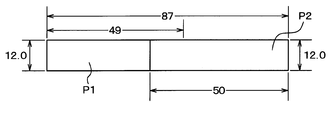
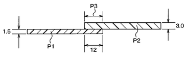
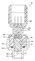
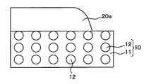
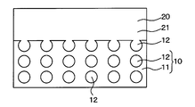
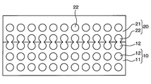
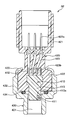
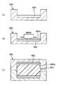
- FIG. 1 is a diagram illustrating a schematic cross-sectional configuration of an electronic device according to a first embodiment of the present disclosure. It is a figure which shows the schematic plane structure of the molded article in Example 1 of this indication. It is a figure which shows schematic sectional structure of the molded article in Example 1 of this indication. It is a figure which shows schematic sectional structure of the pressure sensor as an electronic device concerning 2nd Embodiment of this indication. It is a figure which shows typically the inside of mold resin in 2nd Embodiment. It is a figure which shows typically the state which has arrange
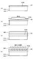
- FIG. (A)-(d) is a figure which shows the manufacturing process of the pressure sensor shown in FIG. (A) to (d) are schematic views of regions A1 to A4 in FIGS. 9 (a) to (d), respectively. It is a figure showing a part of manufacturing process of a pressure sensor as an electronic device concerning a 5th embodiment of this indication.
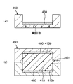
- (A), (b) is a figure which shows a part of manufacturing process of the pressure sensor as an electronic device concerning 6th Embodiment of this indication.
- A)-(c) is a figure which shows the manufacturing process of the pressure sensor following FIG. (a)-(c) is a figure which shows a part of manufacturing process of the pressure sensor as an electronic device concerning 7th Embodiment of this indication.
- the electronic device of the present embodiment is roughly configured to include a first molded product 10 that seals the electronic component 30 and a second molded product 20 that is secondarily molded on the outside of the first molded product 10. ing.
- the electronic component 30 is a passive element such as an IC chip or a capacitor, and the electronic component 30 is mounted on the lead frame 40 via a die bond material (not shown).
- the lead frame 40 has a plate shape made of typical Cu, 42 alloy or the like.
- the electronic component 30 and the lead frame 40 are connected by a bonding wire 50 made of gold, aluminum, or the like, and are electrically connected.
- the first molded product 10 is mainly made of a thermosetting resin and is formed by a transfer molding method or the like.
- the thermosetting resin which comprises this 1st molded object 10 may be mixed with the filler which consists of silica etc. from points, such as adjusting a linear expansion coefficient.
- the electronic component 30, the lead frame 40, and the bonding wire 50 are sealed by the first molded product 10, and the portion of the lead frame 40 opposite to the electronic component 30 is from the first molded product 10. It protrudes.
- the one end side of the terminal pin 60 is connected to the projecting portion of the lead frame 40 from the first molded product 10 by welding or the like.
- the terminal pin 60 is a rod-shaped member made of a Cu-based metal or the like, and is used for electrically connecting the electronic component 30 and the lead frame 40 to the outside.
- the second molded product 20 is mainly made of a thermoplastic resin, and is formed by injection molding or the like.
- the second molded product 20 is provided so as to seal the outside of the first molded product 10 in a state in which the second molded product 20 is in direct contact with the outer surface of the first molded product 10 with respect to a part of the first molded product 10. Yes.
- the second molded product 20 seals the welded portion between the lead frame 40 and the terminal pin 60.
- the 2nd molding 20 and the terminal pin 60 comprise the connector member for making an electrical connection with the exterior in this electronic device.
- the other end side of the terminal pin 60 is exposed at the opening 21 provided in the second molded product 20.
- the opening 21 is configured as an insertion port in the connector member. That is, the second molded product 20 is attached to the external wiring member through the opening 21 and the terminal pin 60 is connected to the external wiring member.
- the first molded article 10 includes the above-described thermosetting resin and further a first additive contained in the thermosetting resin.
- the second molded product 20 includes the above-described thermoplastic resin, and further, a second additive having a reactive group or a skeleton contained in the thermoplastic resin and capable of joining reaction with the first additive. It becomes more.
- the first additive and the second additive are covalently bonded, ionic bond, hydrogen bond, intermolecular force (van der Waals force), Joined by one or more joining actions selected from dispersion force and diffusion.
- the interaction such as a covalent bond refers to one or more bonding actions selected from a covalent bond, an ionic bond, a hydrogen bond, an intermolecular force (Vandere Waals force), a dispersion force, and diffusion. This joining occurs due to molding heat during the secondary molding that forms the second molded product 20.
- thermosetting resin constituting the first molded product 10 and the thermoplastic resin constituting the second molded product 20 are respectively contained in the first additive and the second additive. It is suitable for sealing electronic parts because it is bonded with one or more bonding actions selected from covalent bonds, ionic bonds, hydrogen bonds, intermolecular forces (Van de Waals force), dispersion forces, and diffusion.
- the primary molding method such as the transfer molding method or the compression molding method can firmly secure the adhesion between the molded products 10 and 20.
- the manufacturing method of the electronic device is as follows. First, a first molding material comprising a thermosetting resin and a first additive contained therein is prepared as a raw material for the first molded product 10 (first preparation step).
- a second molding material comprising a thermoplastic resin and a second additive having a reactive group or a skeleton contained therein and capable of bonding reaction with the first additive.
- the second molding material 20 is disposed by placing the second molding material on the outside of the first molding 10 so that the second molding material is brought into direct contact with the outer surface of the first molding 10. Form.
- the first additive and the second additive are covalently bonded, ionic bonded, at the interface between the first molded product 10 and the second molded product 20.
- Joining is performed by one or more joining actions selected from hydrogen bonds, intermolecular forces (van der Waals forces), dispersion forces, and diffusion.
- the second molded product 20 is formed and the connector member is completed, and the electronic device of this embodiment is completed.
- a mold having a cavity corresponding to the outer shape of each final molded product 10 or 20 is used as the above-described mold (not shown).
- the electronic component 30 is first sealed with the first molded product 10 made of a thermosetting resin, and then the outside thereof is made of a thermoplastic resin.
- the second molded product 20 is sealed.
- thermosetting resin constituting the first molded product 10 is obtained by reacting the main agent and the curing agent, in the first molded product 10 of the present embodiment, the main agent and the curing agent are combined. Desirably, the mixture is shifted from the equivalent ratio (10:10).
- the surplus of the main agent and the curing agent is the first additive.
- the 2nd additive in the 2nd molded object 20 should just have a reactive group or frame
- the main agent or the curing agent in the thermosetting resin formed by a chemical reaction between the main agent and the curing agent is used as a surplus, and this is the first additive, another material other than the main agent and the curing agent is used. It can be set as a simple structure, without preparing as a 1st additive.
- the main component of the thermosetting resin and the curing agent constituting the first molded product 10 is the first additive as the surplus
- the second additive in the second molded product 20 As long as it reacts with the main agent, the same main agent and curing agent as the main agent of the first molded product 10 may be used, and further, the main agent and the curing agent of the first molded product 10 are different resins. Also good.
- epoxy resin phenol resin, unsaturated polyester excellent in moisture resistance, chemical resistance, dimensional stability, electrical, mechanical, and thermal properties as the main component of the thermosetting resin constituting the first molded product 10
- resins include resins.
- an epoxy resin is preferable in consideration of versatility and sealing properties.
- thermosetting resin constituting the first molded product 10 usually of a compound having an amino group (NH 2 group) and hydroxyl group (OH group). You may use these main agents and hardening
- the plate piece P1 has a length of 49 mm, a width of 12.0 mm, and a thickness of 1.5 mm
- the plate piece P2 has a length of 50 mm, a width of 12.0 mm, and a thickness of 3. It is 0 mm, and the length of the contact portion P3 is 12 mm.
- the solid matter was taken out by filtration and dried to obtain a phenylene sulfide oligomer having amino groups at both ends.
- the phenylene sulfide oligomer having amino groups at both ends is a PPS skeleton amine.
- FIG. 1 A second embodiment of the present disclosure will be described.
- This embodiment shows an application example to a pressure sensor S1 mounted on a vehicle as an electronic device.
- the pressure sensor S1 detects the pressure of air taken into the engine (intake pressure), the pressure of fuel supplied to the engine, and the like.
- intake pressure the pressure of air taken into the engine
- fuel supplied to the engine the pressure of fuel supplied to the engine
- the connector case 200 includes a connector resin portion 20 and terminal pins 60 sealed by the connector resin portion 20. One end side of the terminal pin 60 is electrically connected to one end side portion of the lead frame 40 exposed from the mold resin 10.
- the housing 300 is connected to the connector case 200 by caulking a part 303 of the housing 300 in a state where the portion on the mold IC 100 side of the connector case 200 is accommodated in the accommodating portion 302.
- An O-ring 304 is interposed between the housing 300 and the connector case 200, and the O-ring 304 seals between the housing 300 and the connector case 200.
- the first additive resin 11 is a thermoplastic resin, and its glass transition temperature or softening point is lower than the molding temperature of the connector resin portion 20 that is the second molded product, and the thermal decomposition temperature is molding of the connector resin portion 20. It is higher than the temperature.
- the molding temperature is about 300 to 340 ° C.
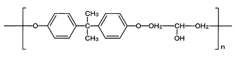
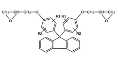
- thermoplastic epoxy resin is typically a resin in which the components shown in FIG. 6B and the components shown in FIG. 6C are mixed.
- R1 to R4 in FIGS. 6B and 6C are hydrogen or an alkyl group.
- This thermoplastic epoxy resin has a softening point of about 80 to 150 ° C. and a remarkable thermal decomposition temperature of about 350 ° C.
- the first additive resin 12 contained in the mold resin 10 has a glass transition temperature or softening point lower than the molding temperature of the connector resin portion 20 and a thermal decomposition temperature of the connector resin portion.
- the molding temperature is higher than 20.
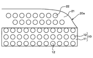
- the base resin 21 is a thermoplastic resin such as PPS or PBT, as in the second embodiment.
- the second additive resin 22 is made of the same thermoplastic resin as the first additive resin 12, and is made of, for example, the phenoxy resin or the thermoplastic epoxy resin.
- the base resin 21 is melted to form the connector resin portion 20 having a desired shape.
- the first additive resin 11 in the mold resin 10 and the connector resin portion 20 are transformed.
- the constituting thermoplastic resin 21 is melted.
- the present disclosure is applied to a pressure sensor mounted on a vehicle.
- This pressure sensor detects the pressure of air taken into the engine (intake pressure), the pressure of fuel supplied to the engine, and the like.
- the mold IC 410 includes a sensor chip 411 as an electronic component, a lead frame 412, and a mold resin 413, and the sensor chip 411 is integrated with the mold resin 413.
- the mold resin 413 is a primary molded body formed of a thermosetting resin such as an epoxy resin. This mold resin 413 also corresponds to the first molded product. The mold resin 413 covers and seals most of the lead frame 412. Although not shown, the mold resin 413 contains a signal processing circuit IC as an electronic component.
- the connector case 420 is integrally formed with a connector portion 421 to which an external connector is connected and a covering portion 422 that covers the terminal 423 and the mold IC 410.
- the connector portion 421 is a portion that outputs a sensor signal to the outside, and has a hollow cylindrical shape inside, and the one end side portion 423a of the terminal 423 is disposed inside the connector portion 421.
- the other end portion 423b of the terminal 423 is electrically connected to the lead frame 412 of the mold IC 410.
- the covering portion 422 covers the terminal 423 connected to the lead frame 412 and the portion of the mold IC 410 on the connector portion 421 side, and exposes the portion of the mold IC 410 on the sensor chip 411 side.
- the housing 430 is a metal case connected to the connector case 420.
- the housing 430 includes a pressure introduction passage 431 that guides the pressure medium to the sensing part of the sensor chip 411 and a housing part 432 that houses a part of the connector case 420.
- the pressure introduction passage 431 is configured as a hollow portion of the housing 430.
- the accommodating portion 432 is configured as an opening at a portion opposite to the pressure introduction passage 431.
- the mold resin 413 of the mold IC 410 is molded so that the photoresponsive compound exists at least on the surface.
- the mold IC 410 and the connector case 420 are in a state in which the photoresponsive compound present on the surface of the mold resin 413 and the thermoplastic resin constituting the connector case 420 are mixed. A junction between the two is formed. In this way, the interface between the mold IC 410 and the connector case 420 is sealed so that the pressure medium does not enter between the mold IC 410 and the connector case 420.
- photoresponsive compound examples include, for example, the liquid crystal compound described in Patent Document 3 represented by the following general formula (2), and the patent document 4 represented by the following general formula (3) or (4).
- the compound represented by the general formula (2) is a solid phase or a liquid crystal phase in the trans isomer, and a liquid phase in the cis isomer.
- R is a group represented by the following general formula (5), and n represents an integer of 1 to 4.
- the compound represented by the general formula (3) or (4) is in a solid phase when in a trans form and in a liquid phase when in a cis form.
- thermosetting resin 531 and the photoresponsive compound 440 are present on the surface 413b of the molded mold resin 413.
- the photoresponsive compound 440 after resin curing forms a trans structure and is a solid phase or a liquid crystal phase.
- the photoresponsive compound molecule 440 is entangled with the photocurable compound molecule and the thermosetting resin molecule, that is, the photoresponsive compound 440 is held in the crosslinked structure of the thermosetting resin reacted with the curing agent through intermolecular force. And fixed to the surface of the mold resin 413. Further, since the holding force is higher than the force applied during the molding of the thermoplastic resin, the photoresponsive compound is held at the interface.
- connection process for connecting the lead frame 412 of the mold IC 410 and the terminal 423 is performed.
- an ultraviolet light irradiation step of irradiating the surface 413b of the mold resin 413 with ultraviolet light is performed.
- the photoresponsive compound 440 existing in the vicinity of the surface of the mold resin 413 forms a cis structure and becomes a liquid phase. That is, the thermosetting resin 531 and the liquid phase photoresponsive compound 440 exist on the surface 413b of the mold resin 413, and the surface 413b of the mold resin 413 is partially liquefied.
- a second molded product molding step is performed in which the connector case 420 is molded with a thermoplastic resin so as to contact the surface 413b of the mold resin 413 irradiated with ultraviolet light.
- the molten thermoplastic resin is injected into the die by an injection method, an extrusion method, or the like.
- the liquid thermoplastic resin comes into contact with the surface 413b of the mold resin 413, as shown in the region surrounded by the broken line in FIG. 10C, the liquid is liquefied like the liquid photoresponsive compound 440.
- a certain thermoplastic resin 601 is mixed, and the molecules are entangled and bonded.
- the connector case 420 is produced by solidifying the liquid thermoplastic resin.
- a phase transition process is performed in which the surface 413b of the mold resin 413 in contact with the connector case 420 is irradiated or heated with visible light.
- the photoresponsive compound 440 changes from a cis structure to a trans structure and undergoes a phase transition from a liquid phase to a solid phase or a liquid crystal phase.
- a bond at the interface between the mold resin 413 of the mold IC 410 and the connector case 420 is formed.
- the connector case 420 and the mold resin 413 are separated if the photoresponsive compound 440 remains in a liquid phase. End up.
- the connector case 420 is fixed to the mold resin 413 by the phase transition of the photoresponsive compound 440 to the solid phase.
- the liquid crystal phase has a higher viscosity than the liquid phase due to the phase transition of the photoresponsive compound 440, the relative movement of the connector case 420 is suppressed, and the connector case 420 is separated from the mold resin 413. It becomes difficult. In this way, the above-mentioned interface junction is formed.
- thermoplastic resin constituting the connector case 420 when visible light irradiation is performed in this phase transition step, when a transparent resin that transmits visible light is used as the thermoplastic resin constituting the connector case 420, the outer surface of the connector case 420 is irradiated with visible light. As a result, visible light is irradiated on the entire surface 413b of the mold resin 413, so that a bond is formed on the entire interface between the mold resin 413 of the mold IC 410 and the connector case 420. On the other hand, when a thermoplastic resin that does not transmit visible light is used as the thermoplastic resin constituting the connector case 420, the exposed interface between the mold resin 413 and the connector case 420 is irradiated with visible light.
- the photoresponsive compound 440 is phase-shifted to a liquid crystal phase having a lower fluidity than a solid phase or a liquid phase, so that the mold resin 413 of the mold IC 410 and The connector case 420 is joined.
- the interface between the mold resin 413 and the connector case 420 is not irradiated with ultraviolet light, so the bonded state at the interface is maintained.
- sealing at the interface between the mold resin 413 made of a thermosetting resin and the connector case 420 made of a thermoplastic resin can be achieved without applying a sealing material after the connector case 420 is molded. it can.
- thermosetting resin molding since a release agent is added to the thermosetting resin, the adhesive force of the thermosetting resin is reduced. For this reason, in order to adhere
- a runner 451 that forms a flow path of a resin injected into a molding die 450 is configured so that ultraviolet light can be irradiated to the resin that passes through the runner 451. Then, when the mold resin 413 is molded using the thermosetting resin mixed with the photoresponsive compound, the thermosetting resin 531 passing through the runner 451 is irradiated with ultraviolet light.
- the surface 413b of the molded mold resin 413 has an optical response between the thermosetting resin 531 and the liquid phase as shown in FIG. 10B.
- the compound 440 exists and the surface 413b of the mold resin 413 is partially liquefied.
- such a first molded product forming step corresponds to a first molded product preparing step.
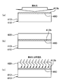
- the mold resin 413 of the mold IC 410 is formed as follows. First, as shown in FIG. 12A, a film 460 made of a photoresponsive compound as a photoresponsive compound layer is prepared, and this film 460 is attached and fixed to the inner surface of a molding die 450. The film 460 can be fixed by evacuation or the like. At this time, the film 460 is disposed on the inner surfaces of the upper mold and the lower mold of the mold 450 so that the film 460 is bonded to the surface 413b of the mold resin 413 that is joined to the connector case 420.
- thermosetting resin 531 is injected into the mold 450 to mold the mold resin 413.
- the mold resin 413 with the film 460 adhered to the surface 413b is produced.
- the thermosetting resin has a higher adhesive force than the thermoplastic resin, the film 460 adheres to the surface of the mold resin 413 by the adhesive force of the thermosetting resin.
- the photoresponsive compound 440 is caused to exist on the surface 413b of the molded mold resin 413 by molding in this way.
- an ultraviolet light irradiation step of irradiating the surface 413b of the mold resin 413, that is, the film 460 with ultraviolet light is performed.
- This step is the same as the step shown in FIG. 9B described in the fourth embodiment.
- the photoresponsive compound present on the surface 413b of the mold resin 413 forms a cis structure and becomes a liquid phase.
- the process from the first molded product forming step to the ultraviolet light irradiation step corresponds to the first molded product preparing step.
- a second molded product is formed by molding the connector case 420 with a thermoplastic resin so as to contact the surface 413b of the mold resin 413 irradiated with ultraviolet light, that is, the film 460. Perform the process.
- This step is the same as the step shown in FIG. 9C of the fourth embodiment.
- the liquid photoresponsive compound and the liquid thermoplastic resin are mixed and the molecules are entangled and bonded.
- a phase transition process is performed in which the surface 413 b of the mold resin 413 that is in contact with the connector case 420, that is, a film 460 is irradiated with visible light or heated.
- This step is the same as the step shown in FIG. 9D of the fourth embodiment.
- the photoresponsive compound of the film 460 changes from a cis structure to a trans structure, and phase transitions from a liquid phase to a solid phase or a liquid crystal phase.
- a bond at the interface between the mold resin 413 of the mold IC 410 and the connector case 420 is formed.
- the interface between the mold resin 413 and the connector case 420 can be sealed without applying a sealing material after the connector case 420 is molded.
- a step of irradiating the film 460 with ultraviolet light is added to increase the adhesive force between the film 460 and the mold resin 413 during the first molded product forming step of the sixth embodiment. is there.
- a film 460 made of a photoresponsive compound is fixed to the inner surface of the mold 450. This step is the same as the step shown in FIG.
- the surface 460a of the film 460 fixed to the inner surface of the mold 450 is irradiated with ultraviolet light.
- the surface 460 a of the film 460 is a surface opposite to the surface in contact with the mold 450 and is a surface in contact with the mold resin 413.
- the portion of the film 460 on the surface 460a side is in a liquid phase with the photoresponsive compound forming a cis structure.
- thermosetting resin 531 is injected into the mold 450 to mold the mold resin 413.
- the liquid curable resin 531 which is in the same liquid state as the liquid photoresponsive compound on the surface 460a side of the film 460 is mixed, so that the molecules are intertwined and bonded to each other, and further, the thermosetting resin 531 Is cured, whereby the film 460 and the mold resin 413 are bonded to each other.
- the adhesive force between the film 460 and the mold resin 413 can be increased.
- FIGS. 13A to 13C are performed as in the sixth embodiment.
- the phase transition process for irradiating visible light or heating and causing the phase transition of the photoresponsive compound shown in FIG. 9D is performed after the second molding molding process. It may be performed during the molding process. That is, in the second molding molding step, a liquid thermoplastic resin is injected into the mold to solidify at least the surface of the connector case 420, and then the connector case 420 is heated and gradually cooled. In the case of performing an annealing process for removing strain, the above-described phase transition process may be performed by heating in this annealing process.
- the photoresponsive compound When the photoresponsive compound undergoes a phase transition from the liquid phase at the heating temperature during the annealing process, the photoresponsive compound can be transformed from the liquid phase to the solid phase or liquid crystal phase simply by performing the annealing process in this manner. It becomes possible.
- the first molded product 10, the second molded product 20, and the manufacturing method thereof are applied to the configuration in which the electronic component is sealed with the first molded product 10.
- the present invention can be applied not only to a configuration in which a part is sealed in the first molded product 10 but also to a configuration integrated with the first molded product 10.
- the present invention is also applicable to a configuration in which electronic components are integrated into the first molded product 10 after molding, such as the pressure sensor of the fourth embodiment.
- the present disclosure is not limited to the above-described embodiment, and can be appropriately changed within the scope described in the claims.
- the said embodiment is not limited to said example of illustration.
- elements constituting the embodiment are not necessarily indispensable except for the case where it is clearly indicated that the element is essential and the case where the element is clearly considered to be essential in principle.
- numerical values such as the number, numerical value, quantity, range, etc. of the constituent elements of the embodiment are mentioned, it is particularly limited to a specific number when clearly indicated as essential and in principle. The number is not limited to a specific number except for cases.
Landscapes
- Engineering & Computer Science (AREA)
- Mechanical Engineering (AREA)
- Manufacturing & Machinery (AREA)
- Microelectronics & Electronic Packaging (AREA)
- Physics & Mathematics (AREA)
- General Physics & Mathematics (AREA)
- Structures Or Materials For Encapsulating Or Coating Semiconductor Devices Or Solid State Devices (AREA)
- Encapsulation Of And Coatings For Semiconductor Or Solid State Devices (AREA)
- Injection Moulding Of Plastics Or The Like (AREA)
Abstract
Priority Applications (3)
| Application Number | Priority Date | Filing Date | Title |
|---|---|---|---|
| US14/414,831 US9789637B2 (en) | 2012-07-16 | 2013-07-10 | Electronic device and method for manufacturing the same |
| DE201311003548 DE112013003548T5 (de) | 2012-07-16 | 2013-07-10 | Elektronische Vorrichtung und Verfahren zum Herstellen derselben |
| CN201380038197.1A CN104471364B (zh) | 2012-07-16 | 2013-07-10 | 电子装置及其制造方法 |
Applications Claiming Priority (6)
| Application Number | Priority Date | Filing Date | Title |
|---|---|---|---|
| JP2012-158220 | 2012-07-16 | ||
| JP2012158220A JP5637189B2 (ja) | 2012-07-16 | 2012-07-16 | 電子装置およびその製造方法 |
| JP2012265313 | 2012-12-04 | ||
| JP2012-265313 | 2012-12-04 | ||
| JP2013032194A JP5772846B2 (ja) | 2012-12-04 | 2013-02-21 | 電子装置およびその製造方法 |
| JP2013-032194 | 2013-02-21 |
Publications (1)
| Publication Number | Publication Date |
|---|---|
| WO2014013697A1 true WO2014013697A1 (fr) | 2014-01-23 |
Family
ID=49948540
Family Applications (1)
| Application Number | Title | Priority Date | Filing Date |
|---|---|---|---|
| PCT/JP2013/004257 Ceased WO2014013697A1 (fr) | 2012-07-16 | 2013-07-10 | Dispositif électronique et son procédé de fabrication |
Country Status (4)
| Country | Link |
|---|---|
| US (1) | US9789637B2 (fr) |
| CN (1) | CN104471364B (fr) |
| DE (1) | DE112013003548T5 (fr) |
| WO (1) | WO2014013697A1 (fr) |
Cited By (11)
| Publication number | Priority date | Publication date | Assignee | Title |
|---|---|---|---|---|
| WO2015079887A1 (fr) * | 2013-11-28 | 2015-06-04 | 日東電工株式会社 | Feuille de résine d'étanchéité thermodurcissable et procédé de fabrication de conditionnement creux |
| JP2015148511A (ja) * | 2014-02-06 | 2015-08-20 | 株式会社デンソー | 圧力センサ |
| WO2015129237A1 (fr) * | 2014-02-27 | 2015-09-03 | 株式会社デンソー | Article moulé en résine et procédé de fabrication pour ce dernier |
| WO2015129236A1 (fr) * | 2014-02-26 | 2015-09-03 | 株式会社デンソー | Corps moulé en résine et procédé de fabrication de celui-ci |
| JP2015162594A (ja) * | 2014-02-27 | 2015-09-07 | 株式会社デンソー | 樹脂成形体およびその製造方法 |
| JP2016082129A (ja) * | 2014-10-20 | 2016-05-16 | 株式会社デンソー | 樹脂成形体およびその製造方法 |
| WO2016103672A1 (fr) * | 2014-12-26 | 2016-06-30 | 株式会社デンソー | Article moulé en résine et son procédé de fabrication |
| JP2016128233A (ja) * | 2015-01-09 | 2016-07-14 | 株式会社デンソー | 樹脂成形体 |
| JP2016203612A (ja) * | 2014-12-26 | 2016-12-08 | 株式会社デンソー | 樹脂成形体およびその製造方法 |
| WO2016208114A1 (fr) * | 2015-06-26 | 2016-12-29 | 株式会社デンソー | Article moulé en résine et son procédé de production |
| EP3203585A4 (fr) * | 2014-09-30 | 2018-04-25 | Century Innovation Corporation | Structure de connexion et son procédé de fabrication, ainsi qu'équipement de transport, équipement de courant électrique, équipement de production d'électricité, équipement médical et équipement spatial |
Families Citing this family (10)
| Publication number | Priority date | Publication date | Assignee | Title |
|---|---|---|---|---|
| DE102013226236A1 (de) * | 2013-12-17 | 2015-06-18 | Robert Bosch Gmbh | Elektrische Baugruppe |
| EP3211732B1 (fr) | 2016-02-24 | 2019-06-26 | PROTECH GmbH | Connecteur et procédé de fabrication d'un connecteur |
| US9870972B2 (en) * | 2015-08-13 | 2018-01-16 | Fuji Electric Co., Ltd. | Thermosetting resin molded article |
| JP6824913B2 (ja) * | 2016-02-09 | 2021-02-03 | 三菱電機株式会社 | 電力用半導体装置及びその製造方法 |
| JP6315025B2 (ja) * | 2016-04-26 | 2018-04-25 | 株式会社デンソー | 物理量センサおよびその製造方法 |
| JP6519533B2 (ja) | 2016-06-09 | 2019-05-29 | 株式会社デンソー | 合成樹脂成形体及びその製造方法 |
| JP6561940B2 (ja) * | 2016-08-12 | 2019-08-21 | 株式会社デンソー | 半導体センサ及びその製造方法 |
| CN110248792A (zh) * | 2017-02-03 | 2019-09-17 | 宝理塑料株式会社 | 树脂成型品的接合方法 |
| DE102017205244A1 (de) | 2017-03-28 | 2018-10-04 | Robert Bosch Gmbh | Mikromechanischer Drucksensor sowie Verfahren zur Herstellung des mikromechanischen Drucksensors |
| DE102018003133A1 (de) * | 2018-04-17 | 2019-10-17 | Infineon Technologies Ag | Sensorvorrichtung, sensormodul, spritzgusswerkzeug und verfahren zur herstellung eines sensormoduls |
Citations (1)
| Publication number | Priority date | Publication date | Assignee | Title |
|---|---|---|---|---|
| JP2002289717A (ja) * | 2001-03-26 | 2002-10-04 | Sony Corp | リードフレーム、電子部品装置及びその製造方法 |
Family Cites Families (22)
| Publication number | Priority date | Publication date | Assignee | Title |
|---|---|---|---|---|
| US5087514A (en) * | 1989-08-30 | 1992-02-11 | Intellex Corporation | Thermoplastic resin layer chemically bonded to thermoset resin layer |
| JPH04144745A (ja) | 1990-10-05 | 1992-05-19 | Mitsubishi Gas Chem Co Inc | 被覆成形品 |
| KR100304813B1 (ko) * | 1992-12-28 | 2001-11-22 | 사와무라 시코 | 부성저항회로와이를사용한슈미트트리거회로 |
| US5948991A (en) | 1996-12-09 | 1999-09-07 | Denso Corporation | Semiconductor physical quantity sensor device having semiconductor sensor chip integrated with semiconductor circuit chip |
| US6259157B1 (en) | 1998-03-11 | 2001-07-10 | Sanyo Electric Co., Ltd. | Hybrid integrated circuit device, and method of manufacturing thereof |
| JP2001305152A (ja) * | 2000-04-18 | 2001-10-31 | Fuji Electric Co Ltd | 半導体センサチップおよびその製造方法、半導体センサチップを備えた半導体センサ |
| JP4134499B2 (ja) * | 2000-08-07 | 2008-08-20 | 住友電気工業株式会社 | 光学装置 |
| JP4174174B2 (ja) * | 2000-09-19 | 2008-10-29 | 株式会社ルネサステクノロジ | 半導体装置およびその製造方法並びに半導体装置実装構造体 |
| EP1367097B1 (fr) * | 2001-02-05 | 2011-06-22 | Toray Industries, Inc. | Composition de resine renforcee par fibres de carbone, materiau a mouler et article moule obtenu a partir de cette composition et de ce materiau |
| JP2002321249A (ja) | 2001-04-25 | 2002-11-05 | Asahi Kasei Corp | インサート成形品とその射出成形方法 |
| JP4620303B2 (ja) * | 2001-09-20 | 2011-01-26 | 株式会社東海理化電機製作所 | 半導体装置及びその製造方法 |
| JP4166997B2 (ja) * | 2002-03-29 | 2008-10-15 | 富士通メディアデバイス株式会社 | 弾性表面波素子の実装方法及び樹脂封止された弾性表面波素子を有する弾性表面波装置 |
| TWI304321B (en) * | 2002-12-27 | 2008-12-11 | Toray Industries | Layered products, electromagnetic wave shielding molded articles and method for production thereof |
| JP4615194B2 (ja) | 2003-04-07 | 2011-01-19 | 株式会社スリオンテック | 光感応性接着性組成物、光感応性接着性シート及びそれを用いた凹凸のある基板の製造方法 |
| JP2004335816A (ja) | 2003-05-09 | 2004-11-25 | Mitsubishi Electric Corp | 電力半導体装置 |
| FR2892124B1 (fr) | 2005-10-18 | 2010-09-10 | Arkema | Composition a base de resines thermoplastiques de pvc plastifiees pour la realisation de peaux composites pour parties d'habitacle de vehicule. |
| JP5212348B2 (ja) * | 2009-12-15 | 2013-06-19 | 株式会社デンソー | 耐燃料性パッケージ |
| JP2011166124A (ja) | 2010-01-14 | 2011-08-25 | Toray Ind Inc | 電気・電子機器筐体 |
| JP5618272B2 (ja) * | 2010-05-10 | 2014-11-05 | 独立行政法人産業技術総合研究所 | 光応答性液晶化合物およびその応用 |
| JP5561728B2 (ja) | 2010-06-10 | 2014-07-30 | 独立行政法人産業技術総合研究所 | 光で化合物を流動化・非流動化させる方法 |
| GB2476703A (en) * | 2010-10-26 | 2011-07-06 | Meiban Int Pte Ltd | Controlling the volume of injected resin in injection moulding |
| JP5435016B2 (ja) * | 2011-12-01 | 2014-03-05 | 株式会社デンソー | 半導体装置の製造方法 |
-
2013
- 2013-07-10 US US14/414,831 patent/US9789637B2/en not_active Expired - Fee Related
- 2013-07-10 DE DE201311003548 patent/DE112013003548T5/de not_active Withdrawn
- 2013-07-10 WO PCT/JP2013/004257 patent/WO2014013697A1/fr not_active Ceased
- 2013-07-10 CN CN201380038197.1A patent/CN104471364B/zh not_active Expired - Fee Related
Patent Citations (1)
| Publication number | Priority date | Publication date | Assignee | Title |
|---|---|---|---|---|
| JP2002289717A (ja) * | 2001-03-26 | 2002-10-04 | Sony Corp | リードフレーム、電子部品装置及びその製造方法 |
Cited By (17)
| Publication number | Priority date | Publication date | Assignee | Title |
|---|---|---|---|---|
| WO2015079887A1 (fr) * | 2013-11-28 | 2015-06-04 | 日東電工株式会社 | Feuille de résine d'étanchéité thermodurcissable et procédé de fabrication de conditionnement creux |
| JP2015148511A (ja) * | 2014-02-06 | 2015-08-20 | 株式会社デンソー | 圧力センサ |
| JP2015162503A (ja) * | 2014-02-26 | 2015-09-07 | 株式会社デンソー | 樹脂成形体およびその製造方法 |
| WO2015129236A1 (fr) * | 2014-02-26 | 2015-09-03 | 株式会社デンソー | Corps moulé en résine et procédé de fabrication de celui-ci |
| CN106030770A (zh) * | 2014-02-27 | 2016-10-12 | 株式会社电装 | 树脂成型体及其制造方法 |
| JP2015162594A (ja) * | 2014-02-27 | 2015-09-07 | 株式会社デンソー | 樹脂成形体およびその製造方法 |
| WO2015129237A1 (fr) * | 2014-02-27 | 2015-09-03 | 株式会社デンソー | Article moulé en résine et procédé de fabrication pour ce dernier |
| CN106030770B (zh) * | 2014-02-27 | 2019-06-18 | 株式会社电装 | 树脂成型体及其制造方法 |
| EP3203585A4 (fr) * | 2014-09-30 | 2018-04-25 | Century Innovation Corporation | Structure de connexion et son procédé de fabrication, ainsi qu'équipement de transport, équipement de courant électrique, équipement de production d'électricité, équipement médical et équipement spatial |
| JP2016082129A (ja) * | 2014-10-20 | 2016-05-16 | 株式会社デンソー | 樹脂成形体およびその製造方法 |
| WO2016103672A1 (fr) * | 2014-12-26 | 2016-06-30 | 株式会社デンソー | Article moulé en résine et son procédé de fabrication |
| CN107108916A (zh) * | 2014-12-26 | 2017-08-29 | 株式会社电装 | 树脂成形体及其制造方法 |
| JP2016203612A (ja) * | 2014-12-26 | 2016-12-08 | 株式会社デンソー | 樹脂成形体およびその製造方法 |
| JP2016128233A (ja) * | 2015-01-09 | 2016-07-14 | 株式会社デンソー | 樹脂成形体 |
| JP2017013238A (ja) * | 2015-06-26 | 2017-01-19 | 株式会社デンソー | 樹脂成形体およびその製造方法 |
| US20180154562A1 (en) * | 2015-06-26 | 2018-06-07 | Denso Corporation | Resin molded article and method for producing same |
| WO2016208114A1 (fr) * | 2015-06-26 | 2016-12-29 | 株式会社デンソー | Article moulé en résine et son procédé de production |
Also Published As
| Publication number | Publication date |
|---|---|
| DE112013003548T5 (de) | 2015-04-02 |
| US9789637B2 (en) | 2017-10-17 |
| US20150158221A1 (en) | 2015-06-11 |
| CN104471364A (zh) | 2015-03-25 |
| CN104471364B (zh) | 2016-10-12 |
Similar Documents
| Publication | Publication Date | Title |
|---|---|---|
| CN104471364B (zh) | 电子装置及其制造方法 | |
| JP5772846B2 (ja) | 電子装置およびその製造方法 | |
| CN1715030B (zh) | 由多个构件构成的部件的结构及其制造方法 | |
| KR101155231B1 (ko) | 광반도체소자 탑재용 패키지 및 이것을 이용한 광반도체장치 | |
| JP2009273104A (ja) | 金属部材とプラスチック部材との接合構造、その製造方法及び電子装置の筐体 | |
| JP2000109709A (ja) | 熱硬化性樹脂材料およびその製造方法 | |
| JP2020166951A (ja) | コネクタ装置 | |
| JP2009029914A5 (fr) | ||
| JP2015093475A (ja) | モールドパッケージおよびその製造方法 | |
| JP5637189B2 (ja) | 電子装置およびその製造方法 | |
| JP2007273796A (ja) | 自動車の電気電子モジュール | |
| JP5930309B2 (ja) | 回転検出装置およびその製造方法 | |
| CN110248468A (zh) | 电子模组及其制造方法及电子装置的壳体及其制造方法 | |
| CN111755874A (zh) | 连接器装置 | |
| CN112054321A (zh) | 连接器装置 | |
| JP2002368183A (ja) | 樹脂封止型モジュール装置及びその製造方法 | |
| JP2015066846A (ja) | 構造体および電池蓋体の製造方法 | |
| JP2014221526A (ja) | 電子装置およびその製造方法 | |
| JP2012254538A (ja) | 複合光学部品の製造方法 | |
| TAKEDA et al. | Development of High Productivity and Low Cost card-edge Type ECU for Motorcycles | |
| KR101914948B1 (ko) | 금속재 이중사출 성형용 수지조성물 | |
| JP2004099886A (ja) | 精密部品用接着剤組成物、これを用いた時計用文字板、および時計用文字板の製造方法 | |
| JP6413951B2 (ja) | 樹脂成形体およびその製造方法 | |
| JP2015032654A (ja) | 電子部品の樹脂封止方法、およびこの樹脂封止方法で電子部品を封止して成る樹脂封止電子部品 | |
| JP2025076130A (ja) | 接合体、接合体の製造方法、撮像モジュール、電子機器、および樹脂組成物 |
Legal Events
| Date | Code | Title | Description |
|---|---|---|---|
| 121 | Ep: the epo has been informed by wipo that ep was designated in this application |
Ref document number: 13820535 Country of ref document: EP Kind code of ref document: A1 |
|
| WWE | Wipo information: entry into national phase |
Ref document number: 14414831 Country of ref document: US |
|
| WWE | Wipo information: entry into national phase |
Ref document number: 1120130035480 Country of ref document: DE Ref document number: 112013003548 Country of ref document: DE |
|
| 122 | Ep: pct application non-entry in european phase |
Ref document number: 13820535 Country of ref document: EP Kind code of ref document: A1 |