WO2014017334A1 - 蛍光体シート - Google Patents
蛍光体シート Download PDFInfo
- Publication number
- WO2014017334A1 WO2014017334A1 PCT/JP2013/069289 JP2013069289W WO2014017334A1 WO 2014017334 A1 WO2014017334 A1 WO 2014017334A1 JP 2013069289 W JP2013069289 W JP 2013069289W WO 2014017334 A1 WO2014017334 A1 WO 2014017334A1
- Authority
- WO
- WIPO (PCT)
- Prior art keywords
- phosphor
- silicon dioxide
- coated
- sulfide
- dioxide film
- Prior art date
- Legal status (The legal status is an assumption and is not a legal conclusion. Google has not performed a legal analysis and makes no representation as to the accuracy of the status listed.)
- Ceased
Links
Images




Classifications
-
- C—CHEMISTRY; METALLURGY
- C08—ORGANIC MACROMOLECULAR COMPOUNDS; THEIR PREPARATION OR CHEMICAL WORKING-UP; COMPOSITIONS BASED THEREON
- C08F—MACROMOLECULAR COMPOUNDS OBTAINED BY REACTIONS ONLY INVOLVING CARBON-TO-CARBON UNSATURATED BONDS
- C08F2/00—Processes of polymerisation
- C08F2/46—Polymerisation initiated by wave energy or particle radiation
- C08F2/48—Polymerisation initiated by wave energy or particle radiation by ultraviolet or visible light
-
- C—CHEMISTRY; METALLURGY
- C09—DYES; PAINTS; POLISHES; NATURAL RESINS; ADHESIVES; COMPOSITIONS NOT OTHERWISE PROVIDED FOR; APPLICATIONS OF MATERIALS NOT OTHERWISE PROVIDED FOR
- C09K—MATERIALS FOR MISCELLANEOUS APPLICATIONS, NOT PROVIDED FOR ELSEWHERE
- C09K11/00—Luminescent materials, e.g. electroluminescent or chemiluminescent
- C09K11/02—Use of particular materials as binders, particle coatings or suspension media therefor
- C09K11/025—Use of particular materials as binders, particle coatings or suspension media therefor non-luminescent particle coatings or suspension media
-
- C—CHEMISTRY; METALLURGY
- C09—DYES; PAINTS; POLISHES; NATURAL RESINS; ADHESIVES; COMPOSITIONS NOT OTHERWISE PROVIDED FOR; APPLICATIONS OF MATERIALS NOT OTHERWISE PROVIDED FOR
- C09K—MATERIALS FOR MISCELLANEOUS APPLICATIONS, NOT PROVIDED FOR ELSEWHERE
- C09K11/00—Luminescent materials, e.g. electroluminescent or chemiluminescent
- C09K11/08—Luminescent materials, e.g. electroluminescent or chemiluminescent containing inorganic luminescent materials
- C09K11/77—Luminescent materials, e.g. electroluminescent or chemiluminescent containing inorganic luminescent materials containing rare earth metals
- C09K11/7728—Luminescent materials, e.g. electroluminescent or chemiluminescent containing inorganic luminescent materials containing rare earth metals containing europium
- C09K11/7729—Chalcogenides
- C09K11/7731—Chalcogenides with alkaline earth metals
-
- C—CHEMISTRY; METALLURGY
- C09—DYES; PAINTS; POLISHES; NATURAL RESINS; ADHESIVES; COMPOSITIONS NOT OTHERWISE PROVIDED FOR; APPLICATIONS OF MATERIALS NOT OTHERWISE PROVIDED FOR
- C09K—MATERIALS FOR MISCELLANEOUS APPLICATIONS, NOT PROVIDED FOR ELSEWHERE
- C09K11/00—Luminescent materials, e.g. electroluminescent or chemiluminescent
- C09K11/08—Luminescent materials, e.g. electroluminescent or chemiluminescent containing inorganic luminescent materials
- C09K11/77—Luminescent materials, e.g. electroluminescent or chemiluminescent containing inorganic luminescent materials containing rare earth metals
- C09K11/7728—Luminescent materials, e.g. electroluminescent or chemiluminescent containing inorganic luminescent materials containing rare earth metals containing europium
- C09K11/7732—Halogenides
- C09K11/7733—Halogenides with alkali or alkaline earth metals
-
- C—CHEMISTRY; METALLURGY
- C09—DYES; PAINTS; POLISHES; NATURAL RESINS; ADHESIVES; COMPOSITIONS NOT OTHERWISE PROVIDED FOR; APPLICATIONS OF MATERIALS NOT OTHERWISE PROVIDED FOR
- C09K—MATERIALS FOR MISCELLANEOUS APPLICATIONS, NOT PROVIDED FOR ELSEWHERE
- C09K11/00—Luminescent materials, e.g. electroluminescent or chemiluminescent
- C09K11/08—Luminescent materials, e.g. electroluminescent or chemiluminescent containing inorganic luminescent materials
- C09K11/77—Luminescent materials, e.g. electroluminescent or chemiluminescent containing inorganic luminescent materials containing rare earth metals
- C09K11/7728—Luminescent materials, e.g. electroluminescent or chemiluminescent containing inorganic luminescent materials containing rare earth metals containing europium
- C09K11/7734—Aluminates
-
- C—CHEMISTRY; METALLURGY
- C09—DYES; PAINTS; POLISHES; NATURAL RESINS; ADHESIVES; COMPOSITIONS NOT OTHERWISE PROVIDED FOR; APPLICATIONS OF MATERIALS NOT OTHERWISE PROVIDED FOR
- C09K—MATERIALS FOR MISCELLANEOUS APPLICATIONS, NOT PROVIDED FOR ELSEWHERE
- C09K11/00—Luminescent materials, e.g. electroluminescent or chemiluminescent
- C09K11/08—Luminescent materials, e.g. electroluminescent or chemiluminescent containing inorganic luminescent materials
- C09K11/77—Luminescent materials, e.g. electroluminescent or chemiluminescent containing inorganic luminescent materials containing rare earth metals
- C09K11/7728—Luminescent materials, e.g. electroluminescent or chemiluminescent containing inorganic luminescent materials containing rare earth metals containing europium
- C09K11/77342—Silicates
-
- F—MECHANICAL ENGINEERING; LIGHTING; HEATING; WEAPONS; BLASTING
- F21—LIGHTING
- F21K—NON-ELECTRIC LIGHT SOURCES USING LUMINESCENCE; LIGHT SOURCES USING ELECTROCHEMILUMINESCENCE; LIGHT SOURCES USING CHARGES OF COMBUSTIBLE MATERIAL; LIGHT SOURCES USING SEMICONDUCTOR DEVICES AS LIGHT-GENERATING ELEMENTS; LIGHT SOURCES NOT OTHERWISE PROVIDED FOR
- F21K9/00—Light sources using semiconductor devices as light-generating elements, e.g. using light-emitting diodes [LED] or lasers
- F21K9/60—Optical arrangements integrated in the light source, e.g. for improving the colour rendering index or the light extraction
- F21K9/64—Optical arrangements integrated in the light source, e.g. for improving the colour rendering index or the light extraction using wavelength conversion means distinct or spaced from the light-generating element, e.g. a remote phosphor layer
-
- G—PHYSICS
- G02—OPTICS
- G02F—OPTICAL DEVICES OR ARRANGEMENTS FOR THE CONTROL OF LIGHT BY MODIFICATION OF THE OPTICAL PROPERTIES OF THE MEDIA OF THE ELEMENTS INVOLVED THEREIN; NON-LINEAR OPTICS; FREQUENCY-CHANGING OF LIGHT; OPTICAL LOGIC ELEMENTS; OPTICAL ANALOGUE/DIGITAL CONVERTERS
- G02F1/00—Devices or arrangements for the control of the intensity, colour, phase, polarisation or direction of light arriving from an independent light source, e.g. switching, gating or modulating; Non-linear optics
- G02F1/01—Devices or arrangements for the control of the intensity, colour, phase, polarisation or direction of light arriving from an independent light source, e.g. switching, gating or modulating; Non-linear optics for the control of the intensity, phase, polarisation or colour
- G02F1/13—Devices or arrangements for the control of the intensity, colour, phase, polarisation or direction of light arriving from an independent light source, e.g. switching, gating or modulating; Non-linear optics for the control of the intensity, phase, polarisation or colour based on liquid crystals, e.g. single liquid crystal display cells
- G02F1/133—Constructional arrangements; Operation of liquid crystal cells; Circuit arrangements
- G02F1/1333—Constructional arrangements; Manufacturing methods
- G02F1/1335—Structural association of cells with optical devices, e.g. polarisers or reflectors
- G02F1/1336—Illuminating devices
- G02F1/133614—Illuminating devices using photoluminescence, e.g. phosphors illuminated by UV or blue light
-
- H—ELECTRICITY
- H10—SEMICONDUCTOR DEVICES; ELECTRIC SOLID-STATE DEVICES NOT OTHERWISE PROVIDED FOR
- H10H—INORGANIC LIGHT-EMITTING SEMICONDUCTOR DEVICES HAVING POTENTIAL BARRIERS
- H10H20/00—Individual inorganic light-emitting semiconductor devices having potential barriers, e.g. light-emitting diodes [LED]
- H10H20/80—Constructional details
- H10H20/85—Packages
- H10H20/851—Wavelength conversion means
- H10H20/8511—Wavelength conversion means characterised by their material, e.g. binder
-
- H—ELECTRICITY
- H10—SEMICONDUCTOR DEVICES; ELECTRIC SOLID-STATE DEVICES NOT OTHERWISE PROVIDED FOR
- H10H—INORGANIC LIGHT-EMITTING SEMICONDUCTOR DEVICES HAVING POTENTIAL BARRIERS
- H10H20/00—Individual inorganic light-emitting semiconductor devices having potential barriers, e.g. light-emitting diodes [LED]
- H10H20/80—Constructional details
- H10H20/85—Packages
- H10H20/851—Wavelength conversion means
- H10H20/8511—Wavelength conversion means characterised by their material, e.g. binder
- H10H20/8512—Wavelength conversion materials
- H10H20/8513—Wavelength conversion materials having two or more wavelength conversion materials
-
- H—ELECTRICITY
- H10—SEMICONDUCTOR DEVICES; ELECTRIC SOLID-STATE DEVICES NOT OTHERWISE PROVIDED FOR
- H10H—INORGANIC LIGHT-EMITTING SEMICONDUCTOR DEVICES HAVING POTENTIAL BARRIERS
- H10H20/00—Individual inorganic light-emitting semiconductor devices having potential barriers, e.g. light-emitting diodes [LED]
- H10H20/80—Constructional details
- H10H20/85—Packages
- H10H20/851—Wavelength conversion means
- H10H20/8514—Wavelength conversion means characterised by their shape, e.g. plate or foil
-
- H—ELECTRICITY
- H10—SEMICONDUCTOR DEVICES; ELECTRIC SOLID-STATE DEVICES NOT OTHERWISE PROVIDED FOR
- H10W—GENERIC PACKAGES, INTERCONNECTIONS, CONNECTORS OR OTHER CONSTRUCTIONAL DETAILS OF DEVICES COVERED BY CLASS H10
- H10W90/00—Package configurations
-
- F—MECHANICAL ENGINEERING; LIGHTING; HEATING; WEAPONS; BLASTING
- F21—LIGHTING
- F21Y—INDEXING SCHEME ASSOCIATED WITH SUBCLASSES F21K, F21L, F21S and F21V, RELATING TO THE FORM OR THE KIND OF THE LIGHT SOURCES OR OF THE COLOUR OF THE LIGHT EMITTED
- F21Y2115/00—Light-generating elements of semiconductor light sources
- F21Y2115/10—Light-emitting diodes [LED]
-
- Y—GENERAL TAGGING OF NEW TECHNOLOGICAL DEVELOPMENTS; GENERAL TAGGING OF CROSS-SECTIONAL TECHNOLOGIES SPANNING OVER SEVERAL SECTIONS OF THE IPC; TECHNICAL SUBJECTS COVERED BY FORMER USPC CROSS-REFERENCE ART COLLECTIONS [XRACs] AND DIGESTS
- Y10—TECHNICAL SUBJECTS COVERED BY FORMER USPC
- Y10T—TECHNICAL SUBJECTS COVERED BY FORMER US CLASSIFICATION
- Y10T428/00—Stock material or miscellaneous articles
- Y10T428/25—Web or sheet containing structurally defined element or component and including a second component containing structurally defined particles
- Y10T428/256—Heavy metal or aluminum or compound thereof
Definitions
- the present invention relates to a phosphor sheet including a phosphor layer formed from a phosphor-containing resin composition containing a film-forming composition and a powdered phosphor that emits fluorescence when irradiated with excitation light.
- LEDs that emit light of three colors of R, G, and B are arranged, and these are turned on at the same time to synthesize light of three colors to obtain white light There is.
- a blue light emitting LED chip is surrounded by a resin contained in a phosphor to convert blue light into white light.
- a phosphor obtained by dispersing a powdery red phosphor that emits red fluorescence when irradiated with blue light and a green phosphor that emits green fluorescence in a resin material excellent in visible light transmission Some sheets obtain white light by emitting light from blue light emitting diodes (blue LEDs) to emit red light and green light, and mixing them with blue light (Patent Document 2, 3).
- the present invention has been proposed in view of such a conventional situation, and provides a phosphor sheet capable of suppressing chromaticity shift and corrosion associated with deterioration of a sulfide phosphor.
- the present inventors have coated the phosphor with a silicon dioxide film, and at least the sulfide phosphor of the phosphor is coated with a silicon dioxide film containing a metal oxide powder.
- the inventors have found that the object can be achieved, and have completed the present invention.
- the phosphor sheet according to the present invention is a phosphor formed of a phosphor-containing resin composition containing a coated phosphor in which the phosphor is coated with a silicon dioxide film, a polymerizable compound, and a polymerization initiator. And a pair of transparent substrates sandwiching the phosphor layer, wherein at least a sulfide phosphor of the phosphor is coated with a silicon dioxide film containing a metal oxide powder. .
- the phosphor-containing resin composition according to the present invention includes a coated phosphor in which the phosphor is coated with a silicon dioxide film, a polymerizable compound, and a polymerization initiator, and at least a sulfide among the phosphors.
- the phosphor is coated with a silicon dioxide film containing a metal oxide powder.
- the lighting device includes a light emitting structure in which a blue-blue light emitting element is included in a transparent resin, a substrate on which the light emitting structure is two-dimensionally arranged, a space apart from the substrate, and the blue light emitting element.
- a phosphor sheet containing a powdered phosphor that obtains white light from blue light of the light emitting element comprising a coated phosphor in which the phosphor is coated with a silicon dioxide film, a polymerizable compound, and A pair of phosphor layers formed of a phosphor-containing resin composition comprising a polymerization initiator and at least a sulfide phosphor among the phosphors coated with a silicon dioxide film containing a metal oxide powder. It is characterized by being sandwiched between transparent substrates.
- the phosphor is coated with a silicon dioxide film, and at least the sulfide phosphor among the phosphors is coated with a silicon dioxide film containing a metal oxide powder. Accompanying chromaticity shift and corrosion can be suppressed.
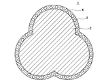
- FIG. 1 is a cross-sectional view showing an example of a coated phosphor according to an embodiment of the present invention.
- FIG. 2 is a cross-sectional view showing an example of a coated phosphor according to an embodiment of the present invention.
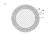
- FIG. 3 is a cross-sectional view showing an example of a coated phosphor according to an embodiment of the present invention.
- FIG. 4 is a cross-sectional view showing an example of a coated phosphor according to an embodiment of the present invention.
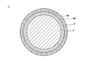
- FIG. 5 is a cross-sectional view showing an example of a coated phosphor according to an embodiment of the present invention.
- FIG. 6 is a cross-sectional view showing an example of a single-layer phosphor sheet.
- FIG. 7 is a cross-sectional view showing an example of a two-layer phosphor sheet.
- FIG. 8 is a cross-sectional view showing an example of a single-layer phosphor sheet laminated with a sealing film.
- FIG. 9 is a cross-sectional view showing an example of a two-layer phosphor sheet laminated with a sealing film.
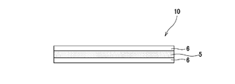
- FIG. 10 is a cross-sectional view showing an example of a sealing film.
- FIG. 11 is a cross-sectional view showing an example of a white light source according to an embodiment of the present invention.
- FIG. 12 is a plan view showing an example of a lighting device according to an embodiment of the present invention.
- FIG. 13 is a cross-sectional view illustrating an example of a lighting device according to an embodiment of the present invention.
- FIG. 14 is a cross-sectional view showing an example of a single-layer phosphor sheet sealed with a sealing film.
- the coated phosphor in the present embodiment is coated with a silicon dioxide film. Thereby, the penetration
- FIG. 1 is a cross-sectional view showing a coated phosphor in which a sulfide phosphor is coated with a silicon dioxide film containing a metal oxide powder.
- a sulfide phosphor 2 is covered with a silicon dioxide film 4 containing a metal oxide powder 3.
- the sulfur-based gas released from the sulfide phosphor 2 by hydrolysis of the sulfide phosphor 2 is Adsorbed on the metal oxide powder 3. Therefore, for example, release of sulfur-based gas from the sulfide phosphor 2 can be suppressed under high temperature and high humidity. Therefore, for example, it is possible to prevent the electrodes and the like from being corroded in the electronic material system, resulting in deterioration of conductivity.
- the sulfide phosphor 2 is not particularly limited.
- SrGa2S4: Eu or CaS: Eu is used.
- the metal oxide powder 3 preferably has a particle size of 0.2 ⁇ m or less.
- the ability of the metal oxide powder 3 to adsorb the sulfur-based gas released from the sulfide phosphor 2 by hydrolysis of the sulfide phosphor 2 by setting the particle size of the metal oxide powder 3 to 0.2 ⁇ m or less. Can be kept from becoming scarce. Thereby, discharge
- the amount of the metal oxide powder 3 is preferably 1 part by mass or more and less than 20 parts by mass, preferably 5 parts by mass or more and 10 parts by mass or less with respect to 100 parts by mass of the sulfide phosphor 2. More preferred. By setting the amount of the metal oxide powder 3 to 1 part by mass or more with respect to 100 parts by mass of the sulfide phosphor 2, an effective adsorption action of the metal oxide powder 3 can be obtained. It is possible to prevent the product powder 3 from having a poor ability to adsorb sulfur-based gas.
- the amount of the metal oxide powder 3 is less than 20 parts by mass with respect to 100 parts by mass of the sulfide phosphor 2, the characteristics of the sulfide phosphor 2, such as peak intensity and luminance, are reduced. This can be prevented.
- the silicon dioxide film 4 is formed on the surface of the sulfide phosphor 2 and covers the surface of the sulfide phosphor 2.
- the silicon dioxide film 4 is produced, for example, by hydrolysis (sol-gel method) of alkoxysilane.
- the thickness of the silicon dioxide film 4 is preferably such that the metal oxide powder 3 is covered with the silicon dioxide film 4.
- the thickness of the silicon dioxide film 4 is preferably 50 to 150 nm.
- the sulfide phosphor 2 is released from the sulfide phosphor 2 by hydrolysis of the sulfide phosphor 2.
- Sulfur-based gas is adsorbed on the metal oxide powder 3. Therefore, for example, release of sulfur-based gas from the sulfide phosphor 2 can be suppressed under high temperature and high humidity.
- the sulfide phosphor 2 does not come into contact with water, it is possible to prevent the sulfide phosphor 2 from being deteriorated by hydrolysis. Thereby, it can prevent that the characteristic of sulfide fluorescent substance 2 falls.
- the coated phosphor 1 may be a secondary particle in which two or more primary particles are connected as shown in FIG. Good. Further, as shown in FIGS. 3 to 5, in the coated phosphor 1, the sulfide phosphor 2 is covered with two or more layers of silicon dioxide film 4, and at least one of the silicon dioxide films 4 has a metal Oxide powder 3 may be contained.
- the coated phosphor 1 includes a two-layered silicon dioxide film 4 on a sulfide phosphor 2, that is, a silicon dioxide film 4 A containing a metal oxide powder 3, and a metal oxide powder.
- the silicon dioxide film 4B containing 3 may be coated in this order.
- the coated phosphor 1 includes a silicon dioxide film 4 ⁇ / b> A containing a metal oxide powder 3 and a silica film, that is, a metal oxide powder 3 on a sulfide phosphor 2.
- the silicon dioxide film 4B that has not been formed may be coated in this order. Further, as shown in FIG.
- the coated phosphor 1 includes a silicon dioxide film 4 ⁇ / b> A that does not contain the metal oxide powder 3 and a silicon dioxide that contains the metal oxide powder 3 on the sulfide phosphor 2.
- the film 4B may be coated in this order.
- coated phosphors 1 shown in FIGS. 3 to 5 at least the silicon dioxide film 4B from the viewpoint of more effectively suppressing the release of sulfur-based gas from the sulfide phosphor 2 under high temperature and high humidity, for example.
- the metal oxide powder 3 is preferably shown in FIGS. 3 and 5. That is, the coated phosphor 1 in which the metal oxide powder 3 is contained in the outermost silicon dioxide film 4B is preferable.
- a method for producing a coated phosphor includes a mixing step in which a phosphor, an alkoxysilane, and a catalyst are mixed in a solvent, and the phosphor is coated with a silicon dioxide film formed from the mixed solution.
- the alkoxysilane can be selected from ethoxide, methoxide, isopropoxide and the like, and examples thereof include tetraethoxysilane and tetramethoxysilane.
- the alkoxysilane may be an alkoxysilane oligomer such as polyethyl silicate or a hydrolysis condensate.
- a silane coupling agent having an alkyl group, an amino group, a mercapto group, or the like that does not contribute to the sol-gel reaction, such as an alkylalkoxysilane, may be used.
- the solvent is not particularly limited, and for example, water, an organic solvent, or the like can be used.
- organic solvent alcohol, ether, ketone, polyhydric alcohol and the like can be used.
- alcohol methanol, ethanol, propanol, pentanol and the like can be used.
- polyhydric alcohols ethylene glycol, propylene glycol, diethylene glycol and the like can be used. Moreover, what combined 2 or more types may be used for a solvent.
- the catalyst is for initiating hydrolysis or polycondensation reaction of alkoxysilane, and for example, an acidic catalyst or a basic catalyst can be used.
- the acidic catalyst include hydrochloric acid, sulfuric acid, boric acid, nitric acid, perchloric acid, tetrafluoroboric acid, hexafluoroarsenic acid, hydrobromic acid, acetic acid, oxalic acid, methanesulfonic acid and the like.
- the basic catalyst include alkali metal hydroxides such as sodium hydroxide, ammonia and the like.
- two or more of these acidic catalysts and basic catalysts may be used in combination.
- the amount of the metal oxide powder is preferably 1 part by mass or more and 20 parts by mass or less with respect to 100 parts by mass of the sulfide phosphor.
- An effective adsorption action of the metal oxide powder can be obtained by blending 1 part by mass or more of the metal oxide powder with respect to 100 parts by mass of the sulfide phosphor. Further, by blending 20 parts by mass or less of metal oxide powder with respect to 100 parts by mass of sulfide phosphor, it is possible to prevent the characteristics of the sulfide phosphor, such as peak intensity and luminance, from being lowered. be able to.
- the mixed phosphor in which the phosphor and alkoxysilane are mixed in a solvent is separated into a solid phase and a liquid phase, whereby a coated phosphor that is a solid phase can be obtained from the mixture.
- a mixed solution is separated into a solid phase and a liquid phase using a suction filter, the separated solid phase is dried, a sample obtained by drying is crushed, and subjected to a firing treatment. Do. Thereby, the coated phosphor in which the phosphor is coated with the silicon dioxide film can be obtained.
- the temperature at which the separated solid phase is dried can be changed according to the solvent used, but is preferably 80 to 110 ° C.
- the time for drying the separated solid phase is preferably 2 hours or longer.
- the temperature for firing the sample is preferably 150 to 250 ° C.
- the time for firing the crushed sample is preferably 8 hours or longer.
- the coated phosphor when the coated phosphor is manufactured, a method of coating the sulfide phosphor with the silicon dioxide film only once, that is, a method of coating the sulfide phosphor with the silicon dioxide film only one layer.
- the silicon dioxide film may be repeatedly coated to coat the phosphor with two or more silicon dioxide films as shown in FIGS.
- the phosphor-containing resin composition in the present embodiment includes a coated phosphor in which the phosphor is coated with a silicon dioxide film, a polymerizable compound, and a polymerization initiator, and at least a sulfide phosphor among the phosphors. Is coated with a silicon dioxide film containing metal oxide powder.
- a red phosphor having a red fluorescence peak with a wavelength of 590 nm to 620 nm by irradiation with blue excitation light and a green fluorescence having a green fluorescence peak with a wavelength of 530 nm to 550 nm by irradiation with blue excitation light It is preferable to use a phosphor mixed with the body.
- red phosphor examples include CaS: Eu, (BaSr) 3 SiO 5 : Eu
- green phosphor examples include inorganic phosphors represented by the following general formula (1).
- M is any one of Ca, Mg, and Ba, and satisfies 0 ⁇ x ⁇ 1 and 0 ⁇ y ⁇ 0.05.
- Specific examples of the green phosphor include SrGa 2 S 4 : Eu.
- a preferred combination in the present embodiment is a mixed phosphor of (BaSr) 3 SiO 5 : Eu that emits red fluorescence and SrGa 2 S 4 : Eu that emits green fluorescence.
- the amount is preferably 1 to 10 parts by mass, more preferably 3 to 6 parts by mass with respect to 100 parts by mass of the resin composition for film formation.
- the polymerizable compound preferably contains a photocurable acrylate. Since the photocurable acrylate has an ester group exhibiting a moisture capturing ability, it is possible to capture more moisture that has entered the phosphor sheet, and to further prevent deterioration of the phosphor due to moisture. Moreover, according to the photocurable acrylate, a phosphor sheet having a small chromaticity shift due to deterioration can be obtained.
- photo-curable acrylates examples include urethane (meth) acrylate, polyester (meth) acrylate, and epoxy acrylate.
- urethane (meth) acrylate can be preferably used from the viewpoint of heat resistance.
- urethane (meth) acrylate a reaction product of a polyol (preferably polyether polyol, polyolefin polyol, polyester polyol or polycarbonate polyol) and a diisocyanate compound (preferably isophorone diisocyanate) is used as a hydroxyalkyl (meth) acrylate. (Preferably, esterified with 21-hydroxypropyl acrylate).
- a polyol preferably polyether polyol, polyolefin polyol, polyester polyol or polycarbonate polyol
- a diisocyanate compound preferably isophorone diisocyanate
- the content of urethane (meth) acrylate is too small, the adhesiveness tends to decrease. Therefore, it is preferable that at least 10 parts by mass is contained in 100 parts by mass of the photocurable acrylate, and at least 30 parts by mass is contained. More preferably.
- the polymerization initiator is preferably a photopolymerization initiator.
- the photopolymerization initiator include radical polymerization initiators such as alkylphenone photopolymerization initiators, acylphosphine oxide photopolymerization initiators, titanocene photopolymerization initiators, oxime ester polymerization initiators, and oxyphenyl acetate esters.
- a cationic polymerization initiator for example, a diazonium polymerization initiator, an iodonium polymerization initiator, a sulphonium polymerization initiator, and the like.
- the amount of these polymerization initiators used is preferably 0.1 to 10 parts by mass, more preferably 1 to 10 parts by mass with respect to 100 parts by mass of the polymerizable compound.
- the phosphor-containing resin composition may be blended with other light-transmitting compounds such as (meth) acrylic monomers and oligomers, coloring pigments and the like, as long as the effects of the present invention are not impaired. it can.
- FIG. 6 is a cross-sectional view of a phosphor sheet according to an embodiment of the present invention.
- a phosphor layer 5 that emits fluorescence when irradiated with excitation light is a single layer sandwiched between a pair of transparent substrates 6, and the phosphor layer 5 is formed from the phosphor-containing resin composition described above. It has been done.
- FIG. 7 is a cross-sectional view of a phosphor sheet having two phosphor layers.
- the phosphor sheet 10 shown in FIG. 6 shows an example in which the phosphor layer 5 is a single layer, but as shown in FIG. 7, two phosphor layers 5 a and 5 b are laminated via a transparent separator 7.
- a laminated phosphor layer 20 having a two-layer structure may be used.
- This phosphor sheet 11 is also sandwiched between a pair of transparent base materials 6a and 6b, similarly to the phosphor sheet 10 shown in FIG.
- one of the phosphor layers 5a and 5b emits red light containing an oxide phosphor (preferably (BaSr) 3 SiO 5 : Eu) having a red fluorescence peak with a wavelength of 590 to 620 nm when irradiated with blue excitation light.
- an oxide phosphor preferably (BaSr) 3 SiO 5 : Eu
- the other is a porous phosphor containing a sulfur-containing phosphor (preferably SrGa 2 S 4 : Eu) having a green fluorescence peak with a wavelength of 530 to 550 nm when irradiated with blue excitation light, and zinc. It is preferable to form from the fluorescent substance containing resin composition containing a crystalline silicate.
- a sulfur-containing phosphor preferably SrGa 2 S 4 : Eu
- the thickness of the phosphor layers 5, 5a, 5b is too thin, the absolute amount of the phosphor is correspondingly reduced, so that sufficient light emission intensity cannot be obtained. On the other hand, if the thickness is too thick, target chromaticity is obtained. Therefore, the thickness is preferably 20 to 150 ⁇ m, more preferably 60 to 120 ⁇ m.
- thermoplastic resin film having a thickness of 10 to 100 ⁇ m a heat or a photocurable resin film can be used.
- examples thereof include a polyester film, a polyamide film, a polyimide film, a polysulfone film, a triacetyl cellulose film, and a polyolefin film.
- the surfaces of these films may be subjected to corona discharge treatment, silane coupling agent treatment, or the like, if necessary.
- the phosphor sheets 10 and 11 shown in FIGS. 6 and 7 are sandwiched between two sealing films 30a and 30b from both sides.
- the phosphor is coated with a silicon dioxide film, and at least the sulfide phosphor of the phosphor is coated with the silicon dioxide film containing the metal oxide powder, as shown in FIGS. Even if the end portion of the phosphor layer is exposed, it is possible to prevent the release of the sulfur-based gas and to further reduce the chromaticity shift.
- the phosphor layer may be a phosphor sheet having an exposed portion between a pair of transparent base materials, it is not necessary to perform a phosphor layer sealing process, and the manufacturing cost of the phosphor sheet can be reduced. It becomes.
- the phosphor sheets 10 and 11 are sealed from both sides with the two sealing films 30a and 30b, the outer circumferences of the two sealing films 30a and 30b and the phosphor sheets 10 and 11 are maintained. It may be sealed with a surrounding frame. By sealing in this way, since the side surfaces of the phosphor sheets 10 and 11 are not exposed, it is possible to further prevent moisture from entering the phosphor layers 5, 5 a and 5 b.
- FIG. 10 is a cross-sectional view showing an example of a sealing film.
- a base film 31 having an adhesive layer 32 formed can be used.
- a silicon oxide layer 33 having a thickness of 5 to 20 nm is formed on the back surface of the base film 31 on the adhesive layer 32 side or the opposite surface by a vapor deposition method or the like. May be.
- the surface protective film 34 may be laminated on the silicon oxide layer 33 via an adhesive layer (not shown).
- the base film 31 and the surface protective film 34 can be used by appropriately selecting from the films exemplified for the transparent substrates 6a and 6b and the transparent separator 7 already described.
- an adhesive layer at the time of laminating the base film 31 and the surface protective film 34 it can be appropriately selected from known adhesives such as urethane adhesives and acrylic adhesives.
- the thickness of the adhesive layer is usually 10 to 50 ⁇ m.
- a single-layer phosphor sheet 10 shown in FIG. 6 forms a phosphor layer 1 by forming a phosphor-containing resin composition on a transparent substrate 6 by a conventional method, and another transparent substrate 6 is formed thereon. It can manufacture by laminating
- the photocurable compound contained in the phosphor layer 5 needs to be photocured (polymerized) by irradiating active energy rays such as ultraviolet rays, for example.
- active energy rays such as ultraviolet rays
- the photocurable compound is directly applied to the phosphor layer 5. You may irradiate an active energy ray, or you may irradiate an active energy ray through the transparent base material 6 or a sealing film.
- the phosphor-containing resin composition is formed on the transparent substrate 6a by a conventional method to form the phosphor layer 5a, and the transparent separator 7 is laminated thereon. Furthermore, another phosphor-containing resin composition containing a phosphor different from the phosphor-containing resin composition is formed by a conventional method to form a phosphor layer 5b, and a transparent substrate 6b is laminated thereon. Can be manufactured. Furthermore, the phosphor sheet 13 having the structure shown in FIG. 9 can be manufactured by sandwiching both surfaces of the phosphor sheet 12 with the sealing films 30a and 30b so that the adhesive layer 32 is on the inner side and thermocompressing the whole. it can.
- the photopolymerizable inclusions contained in the phosphor layers 5a and 5b need to be photocured (polymerized) by irradiating active energy rays such as ultraviolet rays, for example.
- the phosphor layer 5a , 5b may be irradiated with a direct active energy line, or may be irradiated with an active energy ray through the transparent substrates 6a, 6b, the transparent separator 7 and / or the sealing films 30A, 30b. .
- the phosphor-containing resin composition and the phosphor sheet described above can be applied to, for example, a white light source and a lighting device.
- FIG. 11 is a cross-sectional view showing an example of a white light source.
- the white light source 40 has a blue light emitting element 43 on a pad portion 42 formed on an element substrate 41. Electrodes 44 and 45 for supplying electric power for driving the blue light emitting element 43 are formed on the element substrate 41 so as to maintain insulation. The electrodes 44 and 45 are, for example, connected to the blue light emitting element by lead wires 46 and 47, respectively. 43.
- a resin layer 48 is provided around the blue light emitting element 43, and an opening 49 opening on the blue light emitting element 43 is formed in the resin layer 48.
- the opening 49 is formed on an inclined surface whose opening area is widened in the light emitting direction of the blue light emitting element 43, and the reflective film 20 is formed on the inclined surface. That is, the resin layer 48 having the mortar-shaped opening 49 is covered with the reflective film 50 of the opening 49 and the blue light emitting element 43 is disposed on the bottom surface of the opening 49.
- the kneaded material 51 which knead
- a porous silicate containing zinc, a sulfide phosphor having a green fluorescence peak by irradiation with blue excitation light, and a red phosphor having a red fluorescence peak by irradiation with blue excitation light By using a phosphor-containing resin composition containing a polymerizable compound and a polymerization initiator, it is possible to suppress corrosion of the electrodes of the LED element due to sulfur-based gas generated by the deterioration of the sulfide phosphor. it can.
- FIG. 12 is a front view illustrating an example of a lighting device.
- a plurality of white light sources 40 described with reference to FIG. 11 are arranged on the illumination substrate 43.
- the arrangement example may be, for example, a square lattice arrangement as shown in FIG. 12 (A), or an arrangement shifted by 1 ⁇ 2 pitch, for example, every other row as shown in FIG. 12 (B).
- the shifting pitch is not limited to 1/2, and may be 1/3 pitch or 1/4 pitch. Furthermore, you may shift every 1 line or every several lines (for example, 2 lines).
- every other column is shifted by, for example, 1 ⁇ 2 pitch.
- the shifting pitch is not limited to 1/2, and may be 1/3 pitch or 1/4 pitch. Further, it may be shifted every line or every plural lines (for example, 2 lines). That is, how to shift the white light source 10 is not limited.
- the white light source 40 has the same configuration as that described with reference to FIG. That is, the white light source 40 has a kneaded material 51 obtained by kneading a red phosphor and a green phosphor in a transparent resin on the blue light emitting element 43.
- the phosphor-containing resin composition described above is used for the kneaded material 51.
- the illumination device 60 is equivalent to surface light emission because a plurality of white light sources 40 substantially equivalent to point light emission are arranged vertically and horizontally on the illumination substrate 61, so that it is used as a backlight of a liquid crystal display device, for example. be able to.
- the illuminating device 40 can be used for various illuminating devices such as a normal illuminating device, a lighting device for photographing, and a lighting device for construction sites.
- the illumination device 60 uses the white light source 40, it is possible to obtain bright white light with a wide color gamut. For example, when used for a backlight of a liquid crystal display device, pure white with high luminance can be obtained on the display screen, and the quality of the display screen can be improved.
- the lighting device 70 includes a light emitting structure 71 in which a blue light emitting element is covered with a convex surface-shaped transparent resin, a substrate 72 on which the light emitting structure 71 is two-dimensionally arranged, and diffuses blue light from the blue light emitting element.
- the substrate 72 and the phosphor sheet 74 are spaced apart by about 10 to 50 mm, and the lighting device 70 constitutes a so-called remote phosphor structure.
- the gap between the substrate 72 and the phosphor sheet 74 is held by a plurality of support pillars and reflectors, and is provided so that the support pillars and reflectors surround the space formed by the substrate 72 and the phosphor sheet 74 in all directions. .
- the light emitting structure 71 constitutes a so-called LED package having, for example, an InGaN blue LED (Light Emitting Diode) chip as a blue light emitting element.
- LED package having, for example, an InGaN blue LED (Light Emitting Diode) chip as a blue light emitting element.
- the substrate 72 is made of a glass cloth base material using a resin such as phenol, epoxy, polyimide, polyester, bismaleimide triazine, allylated polyphenylene oxide.
- the light emitting structures 71 are two-dimensionally arranged corresponding to the entire surface of the phosphor sheet 74 at equal intervals with a predetermined pitch. Moreover, you may perform a reflection process to the mounting surface of the light emission structure 71 on the board
- the diffusion plate 73 diffuses the radiated light from the light emitting structure 71 over a wide range so that the shape of the light source becomes invisible.
- the diffusing plate 71 one having a total light transmittance of 20% or more and 80% or less is used.
- the phosphor sheet 74 having the structure shown in FIGS. 6 to 9 can be used. That is, a phosphor layer is formed using a phosphor-containing resin composition containing a porous silicate containing zinc, a sulfide phosphor, a polymerizable compound, and a polymerization initiator. Thereby, corrosion of the electrode of the LED element etc. by the sulfur type gas generated by deterioration of sulfide fluorescent substance can be controlled.
- the optical film 75 is composed of, for example, a reflective polarizing film, a lens film, a diffusion film, etc. for improving the visibility of the liquid crystal display device.
- the lens film is an optical film in which minute lenses are arrayed on one surface, and is for increasing the directivity of diffused light in the front direction and increasing the luminance.
- the phosphor contains a coated phosphor coated with a silicon dioxide film, a polymerizable compound, and a polymerization initiator, and at least the sulfide phosphor of the phosphor comprises a metal oxide powder.
- Example> Examples of the present invention will be described below.
- a phosphor sheet having a phosphor layer in which a sulfide phosphor is dispersed in a UV curable acrylic resin is prepared, the luminance and CIE chromaticity of the phosphor sheet are measured, and the chromaticity deviation is evaluated. did.
- production of the sulfur type gas of a fluorescent substance sheet was evaluated.
- the present invention is not limited to these examples.
- the measurement of the brightness and CIE chromaticity of the phosphor sheet, the evaluation of the chromaticity deviation of the phosphor sheet, and the presence or absence of sulfur-based gas generation in the phosphor sheet were measured and evaluated as follows.
- a silver piece test was conducted as an indicator of sulfur gas release. Polishing a piece of silver with a diameter of 15 mm and a thickness of 2 mm (silver bullion (purity 99.95% or more) specified in JIS H 2141 “silver bullion”) with a metal abrasive (Pical, manufactured by Nippon Abrasives Co., Ltd.) And ultrasonically cleaned in acetone. The silver piece after ultrasonic cleaning was attached to the back of the lid of a sealed bottle (100 ml glass weighing bottle) with double-sided tape, and a phosphor sheet (2 cm ⁇ 4 cm) was placed on the bottom inside the sealed bottle.
- Example 1 Into a resin container (PE), 10 g of red phosphor ((Ba, Sr) 3 SiO 6 : Eu), 80 g of ethanol, 5 g of pure water, and 6 g of 28% ammonia water are added, and a magnetic stirrer is added at 40 ° C. After stirring for 10 minutes in a constant temperature bath, 5 g of tetraethoxysilane and 35 g of ethanol were added. Stirring was carried out for 3 hours with the time when the addition was completed as 0 minutes. After the stirring, suction filtration was performed using a vacuum pump, and the collected sample was transferred to a beaker, washed with water or ethanol, and then filtered again to collect the sample. The collected sample was dried at 85 ° C. for 2 hours and baked at 200 ° C. for 8 hours to obtain a coated red phosphor in which the phosphor was coated with a silicon dioxide film.
- PE resin container
- a coating resin composition for film formation containing a photocurable urethane methacrylate (Aronix 1600M, manufactured by Toa Gosei Co., Ltd.) and a photopolymerization initiator (Darocur 1173, manufactured by Nagase Sangyo Co., Ltd.) is coated with 9.0 wt% of the above coated red phosphor. % And 4.5 wt% of the above-mentioned coated green phosphor were uniformly dispersed to obtain a phosphor-containing resin composition.
- the phosphor-containing resin composition is applied onto the first polyethylene terephthalate film so as to have a dry height of 75 ⁇ m, irradiated with ultraviolet rays (7000 mJ / cm 2 ) to polymerize urethane acrylate, and on this phosphor layer.
- the 2nd polyethylene terephthalate film was laminated
- Example 1 A phosphor sheet was obtained in the same manner as in Example 1 except that the green phosphor was used without being coated and was sealed by providing a frame 131 at the end of the phosphor layer 105 as shown in FIG. .
- the relative value of the chromaticity shift of this phosphor sheet was 1.00, and the evaluation of generation of sulfur-based gas was ⁇ .
- Example 2 A phosphor sheet was obtained in the same manner as in Example 1 except that the green phosphor was used without being coated. The relative value of the chromaticity shift of this phosphor sheet was 1.00, and the evaluation of generation of sulfur-based gas was x.
- Example 3 A phosphor sheet was obtained in the same manner as in Example 1 except that zinc oxide powder was not added in the coating treatment of the green phosphor. The relative value of the chromaticity shift of this phosphor sheet was 1.20, and the evaluation of generation of sulfur-based gas was ⁇ .
- Table 1 shows the measurement and evaluation results of Example 1 and Comparative Examples 1 to 3.
- Comparative Example 1 and Comparative Example 2 shows that the release of sulfur-based gas can be suppressed by sealing the end of the phosphor layer. Further, comparing Comparative Example 2 and Comparative Example 3, it can be seen that the release of sulfur-based gas can be suppressed by covering the sulfide phosphor with a silicon dioxide film. Further, when Example 1 and Comparative Example 3 are compared, the release of sulfur-based gas can be sufficiently suppressed by covering the sulfide phosphor with a silicon dioxide film containing zinc oxide powder, and further, chromaticity It can be seen that the deviation can be reduced.
- the phosphor is coated with a silicon dioxide film, and at least the sulfide phosphor among the phosphors is coated with the silicon dioxide film containing the metal oxide powder, whereby the end of the phosphor layer Even with the phosphor sheet exposed, the release of sulfur-based gas can be prevented and the chromaticity shift can be further reduced. For this reason, it is not necessary to perform the sealing process of the phosphor layer, and the manufacturing cost of the phosphor sheet can be reduced.
- SYMBOLS 1 Coated fluorescent substance 2 Sulfide fluorescent substance, 3 Metal oxide powder, 4 Silicon dioxide film, 5, 5a, 5b Phosphor layer, 6, 6a, 6b Transparent base material, 7 Transparent separator 10, 11, 12, 13 phosphor sheet, 20 laminated phosphor layer, 30a, 30b sealing film, 31 base film, 32 adhesive layer, 33 silicon oxide layer, 34 surface protective film, 40 white light source, 41 element substrate, 42 pad portion, 43 blue Light emitting element, 44 electrode, 45 electrode, 46 lead wire, 47 lead wire, 48 resin layer, 49 opening, 50 reflective film, 51 kneaded product, 60 lighting device, 61 lighting substrate, 70 lighting device, 71 light emitting structure, 72 substrate, 73 diffusion plate, 74 phosphor sheet, 75 optical film
Landscapes
- Chemical & Material Sciences (AREA)
- Engineering & Computer Science (AREA)
- Organic Chemistry (AREA)
- Materials Engineering (AREA)
- Inorganic Chemistry (AREA)
- Physics & Mathematics (AREA)
- Optics & Photonics (AREA)
- Chemical Kinetics & Catalysis (AREA)
- Health & Medical Sciences (AREA)
- Medicinal Chemistry (AREA)
- Polymers & Plastics (AREA)
- General Engineering & Computer Science (AREA)
- Microelectronics & Electronic Packaging (AREA)
- Nonlinear Science (AREA)
- Mathematical Physics (AREA)
- Crystallography & Structural Chemistry (AREA)
- General Physics & Mathematics (AREA)
- Luminescent Compositions (AREA)
- Led Device Packages (AREA)
- Polymerisation Methods In General (AREA)
Abstract
硫化物蛍光体の劣化に伴う色度ズレや腐食を抑制する。 蛍光体が二酸化ケイ素膜で被膜された被覆蛍光体と、重合性化合物と、重合開始剤とを含有し、蛍光体のうち少なくとも硫化物蛍光体2が、金属酸化物粉末3を含む二酸化ケイ素膜4で被覆されてなる蛍光体含有樹脂組成物を用いる。これにより、蛍光体層の端部を露出させた蛍光体シートでも、硫黄系ガスの放出を防止することができ、さらに色度ズレを減少させることができる。
Description
本発明は、成膜用組成物と、励起光の照射により蛍光を発する粉末状の蛍光体とを含有する蛍光体含有樹脂組成物から形成された蛍光体層を備える蛍光体シートに関する。
本出願は、日本国において2012年7月25日に出願された日本特許出願番号特願2012-165056を基礎として優先権を主張するものであり、この出願は参照されることにより、本出願に援用される。
本出願は、日本国において2012年7月25日に出願された日本特許出願番号特願2012-165056を基礎として優先権を主張するものであり、この出願は参照されることにより、本出願に援用される。
従来、薄型の液晶ディスプレイは、液晶パネルを背後から前面に照射するバックライトを利用しており、バックライトの構造によりエッジライト方式と直下方式に大別される。
エッジライト方式は、導光板の側面から入射された光を導光板内部に伝播させた後、導光板の上面から取り出すものである。一方、直下方式は、例えば基板上に複数のCCFL(Cold Cathode Fluorescent Lamp)等の蛍光管ランプを配設することにより、全体として面発光を行うものである(特許文献1参照)。
エッジライト方式は、導光板の側面から入射された光を導光板内部に伝播させた後、導光板の上面から取り出すものである。一方、直下方式は、例えば基板上に複数のCCFL(Cold Cathode Fluorescent Lamp)等の蛍光管ランプを配設することにより、全体として面発光を行うものである(特許文献1参照)。
近年、液晶ディスプレイの大型化、薄型化、軽量化、長寿命化や、点滅制御による動画特性改善の観点から、基板上に複数の発光ダイオード(LED)を配設して面発光を行う直下方式が用いられている。
LEDを使用した第1の手法として、R,G,Bの3色の色光をそれぞれ発するLEDを配設し、これらを同時に点灯することにより、3色の光を合成させて白色光を得るものがある。
また、第2の手法として、例えば青色発光LEDチップを、蛍光体に含有した樹脂により包囲し、青色光を白色光に変換するものがある。
また、第3の手法として、青色光の照射により赤色蛍光を発する粉状の赤色蛍光体と緑色蛍光を発する緑色蛍光体とを、可視光透過性に優れた樹脂材料に分散させてなる蛍光体シートに対し、青色発光ダイオード(青色LED)から光を照射して赤色光と緑色光とを発光させ、それらと青色光とを混色させることにより、白色光を得るものがある(特許文献2、3参照)。
ところで、蛍光体は、酸素や水蒸気に対して脆弱なものもあり、酸素や水蒸気等に暴露された場合、特性が劣化し、輝度や色度ムラの原因となる。例えば、硫化物蛍光体は、水分、酸素等の環境劣化を受けやすく、特に高温高湿下において劣化が顕著である。硫化物蛍光体の劣化は、蛍光体自体の硫黄成分がLED素子の通電部分の金属を腐食させ、LED素子内での光取り出し効率の低下、遍電部分の断裂などを惹起するため、LED素子の寿命を短縮させてしまう。
硫化物蛍光体を用いたLED素子の長寿命化を図るため、蛍光体に珪素化合物等よりなる保護層を設ける手法(特許文献4参照)、LED封止樹脂に硫黄系ガス吸着剤を添加する手法(特許文献5参照)、酸素または水蒸気バリアフィルムで封止して長寿命化を図る手法(特許文献6、7参照)も提案されている。
しかしながら、特許文献4のように蛍光体表面を被覆しても、硫化物蛍光体の劣化に伴う色度ズレや腐食を十分に抑制することができない。また、特許文献5~7の技術では、蛍光体自体が保護されておらず、長期の使用で蛍光体の劣化が避けられない。
本発明は、このような従来の実情に鑑みて提案されたものであり、硫化物蛍光体の劣化に伴う色度ズレや腐食を抑制することができる蛍光体シートを提供する。
本件発明者は、鋭意検討を行った結果、蛍光体を二酸化ケイ素膜で被膜し、蛍光体のうち少なくとも硫化物蛍光体を金属酸化物粉末が含有された二酸化ケイ素膜で被膜することにより、上述の目的を達成できることを見出し、本発明を完成させるに至った。
すなわち、本発明に係る蛍光体シートは、蛍光体が二酸化ケイ素膜で被膜された被覆蛍光体と、重合性化合物と、重合開始剤とを含有する蛍光体含有樹脂組成物から形成された蛍光体層と、前記蛍光体層を挟持する一対の透明基材とを備え、前記蛍光体のうち少なくとも硫化物蛍光体が、金属酸化物粉末を含む二酸化ケイ素膜で被覆されてなることを特徴とする。
また、本発明に係る蛍光体含有樹脂組成物は、蛍光体が二酸化ケイ素膜で被膜された被覆蛍光体と、重合性化合物と、重合開始剤とを含有し、前記蛍光体のうち少なくとも硫化物蛍光体が、金属酸化物粉末を含む二酸化ケイ素膜で被覆されてなることを特徴とする。
また、本発明に係る白色光源は、蛍光体が二酸化ケイ素膜で被膜された被覆蛍光体と、重合性化合物と、重合開始剤とを含有し、前記蛍光体のうち少なくとも硫化物蛍光体が、金属酸化物粉末を含む二酸化ケイ素膜で被覆されてなる蛍光体含有樹脂組成物が青色発光素子を覆う状態で硬化してなることを特徴とする。
また、本発明に係る照明装置は、青青色発光素子が透明樹脂で包含された発光構造体と、前記発光構造体が二次元配置された基板と、前記基板と離間して配置され、前記青色発光素子の青色光から白色光を得る粉末状の蛍光体を含有する蛍光体シートとを備え、前記蛍光体シートは、蛍光体が二酸化ケイ素膜で被膜された被覆蛍光体と、重合性化合物と、重合開始剤とを含有し、前記蛍光体のうち少なくとも硫化物蛍光体が、金属酸化物粉末を含む二酸化ケイ素膜で被覆されてなる蛍光体含有樹脂組成物から形成された蛍光体層が一対の透明基材に挟持されてなることを特徴とする。
本発明によれば、蛍光体を二酸化ケイ素膜で被膜し、蛍光体のうち少なくとも硫化物蛍光体を金属酸化物粉末が含有された二酸化ケイ素膜で被膜することにより、硫化物蛍光体の劣化に伴う色度ズレや腐食を抑制することができる。
以下、本発明の実施の形態について、図面を参照しながら下記順序にて詳細に説明する。
1.被覆蛍光体
2.蛍光体含有樹脂組成物
3.蛍光体シート及びその製造方法
4.白色光源、照明装置への適用例
5.実施例
1.被覆蛍光体
2.蛍光体含有樹脂組成物
3.蛍光体シート及びその製造方法
4.白色光源、照明装置への適用例
5.実施例
<1.被覆蛍光体>
本実施の形態における被覆蛍光体は、蛍光体が二酸化ケイ素膜で被膜されている。これにより、蛍光体内部への水分の浸入を防止し、水分による蛍光体の劣化を防止することができる。また、蛍光体のうち少なくとも硫化物蛍光体は、金属酸化物粉末を含む二酸化ケイ素膜で被覆される。これにより、硫化物蛍光体の劣化による硫化水素や二酸化硫黄を主成分とする硫黄系ガスの放出を防止することができる。したがって、本実施の形態における被覆蛍光体を用いることにより、蛍光体含有樹脂組成物で形成される蛍光体層の色度ズレや、LED素子の電極等の腐食を抑制することができる。
本実施の形態における被覆蛍光体は、蛍光体が二酸化ケイ素膜で被膜されている。これにより、蛍光体内部への水分の浸入を防止し、水分による蛍光体の劣化を防止することができる。また、蛍光体のうち少なくとも硫化物蛍光体は、金属酸化物粉末を含む二酸化ケイ素膜で被覆される。これにより、硫化物蛍光体の劣化による硫化水素や二酸化硫黄を主成分とする硫黄系ガスの放出を防止することができる。したがって、本実施の形態における被覆蛍光体を用いることにより、蛍光体含有樹脂組成物で形成される蛍光体層の色度ズレや、LED素子の電極等の腐食を抑制することができる。
図1は、硫化物蛍光体が金属酸化物粉末を含有する二酸化ケイ素膜で被覆された被覆蛍光体を示す断面図である。この被覆蛍光体1は、硫化物蛍光体2が、金属酸化物粉末3が含有された二酸化ケイ素膜4によって被覆されている。金属酸化物粉末3が含有された二酸化ケイ素膜4によって硫化物蛍光体2が被覆されていることにより、硫化物蛍光体2の加水分解によって硫化物蛍光体2から放出される硫黄系ガスが、金属酸化物粉末3に吸着される。そのため、例えば高温高湿下において硫化物蛍光体2からの硫黄系ガスの放出を抑制することができる。したがって、例えば、電子材料系において電極等が腐食され、導電性の悪化等を招いてしまうことを防止することができる。
硫化物蛍光体2としては、特に限定されないが、例えば、SrGa2S4:EuやCaS:Euが用いられる。硫化物蛍光体2は、例えば、メジアン径(d50)が、5~15μm程度のものを用いることができる。
金属酸化物粉末3としては、硫黄系ガス、例えば、硫化水素を吸着する能力に優れ、硫黄系ガスの抑制効果を奏することができるものが好ましい。このような金属酸化物粉末3としては、例えば、酸化亜鉛粉末や酸化アルミニウム(Al2O3)粉末が挙げられ、特に、硫黄系ガスの抑制効果をより効果的に奏することができる観点から、酸化亜鉛粉末を用いることが好ましい。また、金属酸化物粉末3としては、表面処理を施したものを用いてもよい。
金属酸化物粉末3は、粒径が0.2μm以下であることが好ましい。金属酸化物粉末3の粒径を0.2μm以下とすることにより、硫化物蛍光体2の加水分解によって硫化物蛍光体2から放出される硫黄系ガスを、金属酸化物粉末3が吸着する能力が乏しくならないようにすることができる。これにより、硫化物蛍光体2からの硫黄系ガスの放出を効果的に抑制することができる。
金属酸化物粉末3の量は、100質量部の硫化物蛍光体2に対して、1質量部以上、20質量部未満とすることが好ましく、5質量部以上、10質量部以下とすることがより好ましい。100質量部の硫化物蛍光体2に対して、金属酸化物粉末3の量を1質量部以上とすることにより、金属酸化物粉末3の有効な吸着作用を得ることができる、すなわち、金属酸化物粉末3が硫黄系ガスを吸着する能力が乏しくならないようにすることができる。また、100質量部の硫化物蛍光体2に対して、金属酸化物粉末3の量を20質量部未満とすることにより、硫化物蛍光体2の特性、例えばピーク強度や輝度が低下してしまうことを防止することができる。
二酸化ケイ素膜4は、硫化物蛍光体2の表面に形成され、硫化物蛍光体2の表面を被覆する。硫化物蛍光体2を二酸化ケイ素膜4によって被覆させることにより、硫化物蛍光体2が水と触れないようにして、加水分解によって硫化物蛍光体2が劣化してしまうことを防止することができる。これにより、硫化物蛍光体2の特性、例えば、発光強度や輝度が低下してしまうことを防止することができ、硫化物蛍光体2の特性を維持することができる。二酸化ケイ素膜4は、例えば、アルコキシシランの加水分解(ゾルゲル法)によって生成されている。
二酸化ケイ素膜4の厚さは、二酸化ケイ素膜4によって金属酸化物粉末3が覆われる程度とすることが好ましい。例えば、粒径が0.2μm以下の金属酸化物粉末3を用いた場合には、二酸化ケイ素膜4の厚さは、50~150nmとすることが好ましい。二酸化ケイ素膜4の厚さを50nm以上とすることにより、加水分解によって硫化物蛍光体2が劣化してしまうことをより効果的に防止することができる。また、二酸化ケイ素膜4の厚さを150nm以下とすることにより、硫化物蛍光体2の特性、例えばピーク強度や輝度が低下してしまうことを防止することができる。
上述したように、硫化物蛍光体2が、金属酸化物粉末3を含有する二酸化ケイ素膜4によって被覆されていることにより、硫化物蛍光体2の加水分解によって硫化物蛍光体2から放出される硫黄系ガスが金属酸化物粉末3に吸着される。そのため、例えば高温高湿下において硫化物蛍光体2からの硫黄系ガスの放出を抑制することができる。また、硫化物蛍光体2が水と触れないため、加水分解によって硫化物蛍光体2が劣化してしまうことを防止することができる。これにより、硫化物蛍光体2の特性が低下してしまうことを防止することができる。
また、被覆蛍光体1は、図1に示すように、単位粒子と考えられるものを一次粒子としたときに、図2に示すように、一次粒子が2以上連結した二次粒子であってもよい。また、被覆蛍光体1は、図3~図5に示すように、硫化物蛍光体2が、二層以上の二酸化ケイ素膜4によって被覆されており、少なくともいずれかの二酸化ケイ素膜4中に金属酸化物粉末3が含有されていてもよい。
図3に示すように、被覆蛍光体1は、硫化物蛍光体2上に、二層の二酸化ケイ素膜4、すなわち、金属酸化物粉末3が含有された二酸化ケイ素膜4Aと、金属酸化物粉末3が含有された二酸化ケイ素膜4Bとがこの順番で被覆されていてもよい。また、図4に示すように、被覆蛍光体1は、硫化物蛍光体2上に、金属酸化物粉末3が含有された二酸化ケイ素膜4Aと、シリカ皮膜、すなわち、金属酸化物粉末3が含有されていない二酸化ケイ素膜4Bとがこの順番で被覆されていてもよい。さらに、図5に示すように、被覆蛍光体1は、硫化物蛍光体2上に、金属酸化物粉末3が含有されていない二酸化ケイ素膜4Aと、金属酸化物粉末3が含有された二酸化ケイ素膜4Bとがこの順番で被覆されていてもよい。
これらの図3~図5に示す被覆蛍光体1の中では、例えば高温高湿下において硫化物蛍光体2からの硫黄系ガスの放出をより効果的に抑制する観点から、少なくとも二酸化ケイ素膜4Bに金属酸化物粉末3が含有されている図3及び図5に示すものが好ましい。すなわち、最表面側の二酸化ケイ素膜4Bに金属酸化物粉末3が含有されている被覆蛍光体1が好ましい。
被覆蛍光体の製造方法は、蛍光体と、アルコキシシランと、触媒とを溶媒中で混合し、混合液から形成される二酸化ケイ素膜によって蛍光体を被覆させる混合工程と、混合液を固相と液相とに分離する分離工程とを有する。硫化物蛍光体を被覆する場合、混合工程において、硫化物蛍光体と、アルコキシシランと、金属酸化物粉末と、触媒とを溶媒中で混合し、混合液から形成される二酸化ケイ素膜によって蛍光体を被覆させる。
アルコキシシランは、エトキシド、メトキシド、イソプロポキシド等から選択することができ、例えば、テトラエトキシシランやテトラメトキシシランが挙げられる。また、アルコキシシランは、ポリエチルシリケート等のアルコキシシランオリゴマーや加水分解縮合物であってもよい。さらに、アルコキシシランは、アルキルアルコキシシラン等のように、ゾルゲル反応に寄与しないアルキル基、アミノ基、メルカプト基等を有するシランカップリング剤を用いてもよい。
溶媒は、特に限定されず、例えば、水、有機溶媒等を用いることができる。有機溶媒としては、アルコール、エーテル、ケトン、多価アルコール類等を用いることができる。アルコールとしては、メタノール、エタノール、プロパノール、ペンタノール等を用いることができる。多価アルコール類としては、エチレングリコール、プロピレングリコール、ジエチレングリコール等を用いることができる。また、溶媒は、二種以上を組み合わせたものを用いてもよい。
触媒は、アルコキシシランの加水分解や重縮合反応を開始させるためのものであり、例えば、酸性触媒や塩基性触媒を用いることができる。酸性触媒しては、塩酸、硫酸、ホウ酸、硝酸、過塩素酸、テトラフルオロホウ酸、ヘキサフルオロ砒素酸、臭化水素酸、酢酸、シュウ酸、メタンスルホン酸等が挙げられる。塩基性触媒としては、水酸化ナトリウムなどのアルカリ金属の水酸化物、アンモニア等が挙げられる。これらの触媒の中では、硫化物蛍光体2の劣化を効果的に防止する観点から、塩基性触媒を用いることが好ましい。なお、触媒としては、これらの酸性触媒や塩基性触媒を二種以上併用してもよい。
混合工程において、硫化物蛍光体を被覆する場合、金属酸化物粉末の配合量は、100質量部の硫化物蛍光体に対して、1質量部以上20質量部以下とすることが好ましい。100質量部の硫化物蛍光体に対して、1質量部以上の金属酸化物粉末を配合することにより、金属酸化物粉末の有効な吸着作用を得ることができる。また、100質量部の硫化物蛍光体に対して、20質量部以下の金属酸化物粉末を配合することにより、硫化物蛍光体の特性、例えばピーク強度や輝度が低下してしまうことを防止することができる。
分離工程では、蛍光体とアルコキシシランとを溶媒中で混合させた混合液を固相と液相とに分離することにより、固相である被覆蛍光体を混合液中から得ることができる。
例えば、分離工程においては、吸引濾過器を用いて、混合液を固相と液相とに分離し、分離した固相を乾燥し、乾燥して得られた試料を解砕し、焼成処理を行う。これにより、二酸化ケイ素膜によって蛍光体が被覆された被覆蛍光体を得ることができる。
分離した固相を乾燥させる温度は、使用する溶媒に応じて変更することが可能であるが、80~110℃とすることが好ましい。また、分離した固相を乾燥させる時間は、2時間以上とすることが好ましい。
試料を焼成する温度は、150~250℃とすることが好ましい。また、粉砕した試料を焼成する時間は、8時間以上とすることが好ましい。
なお、上述した説明では、被覆蛍光体を製造する際に、硫化物蛍光体に対する二酸化ケイ素膜の被覆処理を1回だけ行う方法、すなわち、硫化物蛍光体に二酸化ケイ素膜を一層だけ被覆させる方法について説明したが、この例に限定されるものではない。例えば、二酸化ケイ素膜の被覆処理を繰り返し行って、図3~5に示すように、蛍光体に二層以上の二酸化ケイ素膜を被覆させるようにしてもよい。
<2.蛍光体含有樹脂組成物>
本実施の形態における蛍光体含有樹脂組成物は、蛍光体が二酸化ケイ素膜で被膜された被覆蛍光体と、重合性化合物と、重合開始剤とを含有し、蛍光体のうち少なくとも硫化物蛍光体が、金属酸化物粉末を含む二酸化ケイ素膜で被覆されている。青色LEDを用いて白色を発光させる場合、青色励起光の照射により波長590nm~620nmの赤色蛍光ピークを有する赤色蛍光体と、青色励起光の照射により波長530nm~550nmの緑色蛍光ピークを有する緑色蛍光体との混合蛍光体を使用することが好ましい。
本実施の形態における蛍光体含有樹脂組成物は、蛍光体が二酸化ケイ素膜で被膜された被覆蛍光体と、重合性化合物と、重合開始剤とを含有し、蛍光体のうち少なくとも硫化物蛍光体が、金属酸化物粉末を含む二酸化ケイ素膜で被覆されている。青色LEDを用いて白色を発光させる場合、青色励起光の照射により波長590nm~620nmの赤色蛍光ピークを有する赤色蛍光体と、青色励起光の照射により波長530nm~550nmの緑色蛍光ピークを有する緑色蛍光体との混合蛍光体を使用することが好ましい。
赤色蛍光体としては、CaS:Eu、(BaSr)3SiO5:Euなどが挙げられ、緑色蛍光体としては、例えば下記一般式(1)で表わされる無機蛍光体が挙げられる。
(SrxM1-x-y)Ga2S4:Euy (1)
式(1)中、MはCa、Mg、Baのいずれかであり、0≦x≦1、0<y<0.05を満たす。具体的な緑色蛍光体としては、例えばSrGa2S4:Euなどが挙げられる。
本実施の形態における好ましい組み合わせは、赤色蛍光を発する(BaSr)3SiO5:Euと、緑色蛍光を発するSrGa2S4:Euとの混合蛍光体である。
被覆蛍光体の成膜用樹脂組成物に対する混合割合は、少なすぎると、塗布膜が厚くなり使用する溶剤量が多くなる傾向があり、多すぎると、塗布膜が薄くなり、色度ムラが大きくなる傾向があるので、成膜用樹脂組成物100質量部に対し、好ましくは1~10質量部、より好ましくは3~6質量部である。
重合性化合物は、光硬化型アクリレートを含有することが好ましい。光硬化型アクリレートは、水分捕捉能を示すエステル基を有するため、蛍光体シートに浸入した水分をより捕捉することが可能となり、水分による蛍光体の変質をより防止することが可能となる。また、光硬化型アクリレートによれば、劣化による色度ズレが小さい蛍光体シートを得ることができる。
このような光硬化型アクリレートとしては、ウレタン(メタ)アクリレート、ポリエステル(メタ)アクリレート、エポキシアクリレートなどを挙げることができる。これらの中でも、耐熱性の点からウレタン(メタ)アクリレートを好ましく使用することができる。
好ましいウレタン(メタ)アクリレートとしては、ポリオール(好ましくはポリエーテルポリオール、ポリオレフィンポリオール、ポリエステルポリオールもしくはポリカーポネートボリオール)とジイソシアネート化合物(好ましくはイソホロンジイソシアネート)との反応物を、ヒドロキシアルキル(メタ)アクリレート(好ましくは、2一ヒドロキシプロピルアクリレート)でエステル化したものが挙げられる。
ウレタン(メタ)アクリレートの含有量が少なすぎると、接着性が低下する傾向があるため、光硬化型アクリレート100質量部中に少なくとも10質量部含有されていることが好ましく、少なくとも30質量部含有されていることがより好ましい。
重合開始剤は、光重合開始剤であることが好ましい。光重合開始剤としては、ラジカル重合開始剤、例えば、アルキルフェノン系光重合開始剤、アシルフォスフィンオキサイド系光重合開始剤、チタノセン系光重合開始剤、オキシムエステル系重合開始剤、オキシフェニル酢酸エステル系重合開始剤等;カチオン重合開始剤、例えば、ジアゾニウム系重合開始剤、ヨードニウム系重合開始剤、スルポニウム系重合開始剤等を挙げることができる。これらの重合開始剤の使用量は、重合性化合物100質量部に対し、好ましくは0.1~10質量部、より好ましくは1~10質量部である。
また、蛍光体含有樹脂組成物には、必要に応じ、本発明の効果を損なわない範囲で、(メタ)アクリル系モノマー、オリゴマー等の他の光透過性化合物、着色顔料等を配合することができる。
<3.蛍光体シート及びその製造方法>
次に、蛍光体含有樹脂組成物を使用した蛍光体シートについて、図面を参照しながら説明する。
次に、蛍光体含有樹脂組成物を使用した蛍光体シートについて、図面を参照しながら説明する。
図6は、本発明の一実施の形態に係る蛍光体シートの断面図である。この蛍光体シート10は、励起光の照射により蛍光を発する蛍光体層5が単層で一対の透明基材6に挟持され、蛍光体層5が、前述した蛍光体含有樹脂組成物で成膜されたものである。
また、図7は、蛍光体層が2層の蛍光体シートの断面図である。図6に示す蛍光体シート10は、蛍光体層5が単層である例を示したが、図7に示すように、透明セパレータ7を介して2層の蛍光体層5a,5bを積層した2層構造の積層蛍光体層20としてもよい。この蛍光体シート11も、図6に示す蛍光体シート10と同様に、一対の透明基材6a,6bに挟持させる。このように2層構造とすることにより、互いに反応し易い蛍光体同士(例えばCaS:EuとSrCa2S4:Eu)、蛍光体と樹脂成分とを別々の層に配置できる。その結果、それらの意図しない反応を抑制することができ、蛍光体シートの寿命を長くすることができる。この場合、蛍光体層5a,5bの一方を、青色励起光の照射により波長590~620nmの赤色蛍光ピークを有する酸化物蛍光体(好ましくは(BaSr)3SiO5:Eu)を含有する赤色発光の蛍光体含有樹脂組成物から形成し、他方を、青色励起光の照射により波長530~550nmの緑色蛍光ピークを有する硫化系蛍光体(好ましくはSrGa2S4:Eu)と、亜鉛を含む多孔質ケイ酸塩とを含有する蛍光体含有樹脂組成物から形成することが好ましい。
蛍光体層5,5a,5bの厚みは、薄すぎると相応して蛍光体の絶対量が少なくなるので十分な発光強度を得ることができず、他方、厚すぎるとターゲットとなる色度が得られないので、好ましくは20~150μm、より好ましくは60~120μmである。
透明基材6a,6bや透明セパレータ7としては、厚さ10~100μmの熱可塑性樹脂フィルム、熱又は光硬化性樹脂フィルムを使用することができる。例えば、ポリエステルフィルム、ポリアミドフィルム、ボリイミドフィルム、ポリスルホンフィルム、トリアセチルセルロースフィルム、ポリオレフィンフィルム等を挙げることができる。これらのフィルムの表面には、蛍光体含有樹脂組成物に対する密着性を改善するために、必要に応じて、コロナ放電処理、シランカッブリング剤処理等を施してもよい。
また、図8及び図9に示すように、図6及び図7に示す蛍光体シート10,11を、その両面から、2枚の封止フィルム30a,30bで挟持することが好ましい。本実施の形態では、蛍光体を二酸化ケイ素膜で被膜し、蛍光体のうち少なくとも硫化物蛍光体を金属酸化物粉末を含む二酸化ケイ素膜で被覆するため、図8及び図9に示すように、蛍光体層の端部を露出させても、硫黄系ガスの放出を防止することができ、さらに色度ズレを減少させることができる。すなわち、蛍光体層が一対の透明基材の間に露出部を有する蛍光体シートでもよいため、蛍光体層の封止処理を行う必要がなく、蛍光体シートの製造コストを削減することが可能となる。もちろん、蛍光体シート10,11を、その両面から、2枚の封止フィルム30a,30bで封止しても、2枚の封止フィルム30a,30bと、蛍光体シート10,11の外周を囲う額縁とで封止しても構わない。このように封止することにより、蛍光体シート10,11の側面が露出しないため、蛍光体層5,5a,5bへの水分の浸入をより防止することができる。
図10は、封止フィルムの一例を示す断面図である。この封止フィルムは、ベースフィルム31に接着層32が形成されたものを使用することができる。また、封止フィルムの水蒸気バリア性を向上させるために、接着層32側のベースフィルム31の裏面またはその反対側の表面に、厚さ5~20nmの酸化ケイ素層33を蒸着法等により形成してもよい。後者の場合、酸化ケイ素層33上に、接着層(図示せず)を介して表面保護フィルム34を積層してもよい。ベースフィルム31や表面保護フィルム34としては、既に説明した透明基材6a、6bや透明セパレータ7で例示したフィルムの中から適宜選択して使用することができる。ベースフィルム31及び表面保護フィルム34の積層の際の接着層としては、ウレタン系接着剤、アクリル系接着剤等、公知の接着剤の中から適宜選択して使用することができる。また、接着層の厚みは、通常10~50μmである。
次に、蛍光体シートの製造方法について、図面を参照しながら説明する。図6に示す単層型の蛍光体シート10は、透明基材6に蛍光体含有樹脂組成物を常法により成膜して蛍光体層1を形成し、その上に別の透明基材6を積層することにより製造することができる。さらに、蛍光体シート10の両面を接着層32が内側となるように封止フィルム30a,30bで挟み、全体を熱圧着することにより、図8に示す構造の蛍光体シート12を製造することができる。
なお、蛍光体層5に含まれる光硬化性化合物に対して、例えば紫外線等の活性エネルギー線を照射して光硬化(重合)させる必要があるが、この場合、蛍光体層5に対して直接活性エネルギー線を照射してもよいし、又は透明基材6越し若しくは封止フィルム越しに活性エネルギー線を照射してもよい。
図8に示す2層型の蛍光体シート12は、透明基材6aに蛍光体含有樹脂組成物を常法により成膜して蛍光体層5aを形成し、その上に透明セパレータ7を積層し、さらに、先の蛍光体含有樹脂組成物と異なる蛍光体を含む別の蛍光体含有樹脂組成物を常法により成膜して蛍光体層5bを形成し、その上に透明基材6bを積層することにより製造することができる。さらに、蛍光体シート12の両面を接着層32が内側となるように封止フィルム30a,30bで挟み、全体を熱圧着することにより、図9に示す構造の蛍光体シート13を製造することができる。
なお、蛍光体層5a,5bに含まれる光重合性化含物に対して、例えば紫外線等の活性エネルギー線を照射して光硬化(重合)させる必要があるが、この場合、蛍光体層5a,5bに対して直接の活性工ネルギー線を照射してもよいし、又は透明基材6a,6b、透明セパレータ7及び/又は封止フィルム30A,30b越しに活性エネルギー線を照射させてもよい。
<4.白色光源、照明装置への適用例>
前述した蛍光体含有樹脂組成物及び蛍光体シートは、例えば、白色光源や照明装置に適用することができる。
前述した蛍光体含有樹脂組成物及び蛍光体シートは、例えば、白色光源や照明装置に適用することができる。
<4-1.白色光源>
図11は、白色光源の一例を示す断面図である。図11に示すように、白色光源40は、素子基板41上に形成されたパッド部42上に青色発光素子43を有している。素子基板41には、青色発光素子43を駆動するための電力を供給する電極44,45が絶縁性を保って形成され、それぞれの電極44,45は、例えばリード線46,47によって青色発光素子43に接続されている。
図11は、白色光源の一例を示す断面図である。図11に示すように、白色光源40は、素子基板41上に形成されたパッド部42上に青色発光素子43を有している。素子基板41には、青色発光素子43を駆動するための電力を供給する電極44,45が絶縁性を保って形成され、それぞれの電極44,45は、例えばリード線46,47によって青色発光素子43に接続されている。
また、青色発光素子43の周囲には、例えば樹脂層48が設けられ、その樹脂層48には、青色発光素子43上を開口する開口部49が形成されている。この開口部49には、青色発光素子43の発光方向に開口面積が広くなる傾斜面に形成され、その傾斜面には反射膜20が形成されている。すなわち、すり鉢状の開口部49を有する樹脂層48において、開口部49の反射膜50で覆われ、開口部49の底面に青色発光素子43が配置された状態となっている。そして、開口部49内に、赤色蛍光体と緑色蛍光体とを透明樹脂に混練した混練物51が、青色発光素子43を覆う状態で硬化し、白色光源40が構成されている。
ここで、混練物51として、亜鉛を含む多孔質ケイ酸塩と、青色励起光の照射により緑色蛍光ピークを有する硫化物蛍光体と、青色励起光の照射により赤色蛍光ピークを有する赤色蛍光体と、重合性化合物と、重合開始剤とを含有する蛍光体含有樹脂組成物を使用することにより、硫化物蛍光体の劣化によって発生する硫黄系ガスによるLED素子の電極等の腐食を抑制することができる。
<4-2.照明装置>
図12は、照明装置の一例を示す正面図である。図12に示すように、照明装置60は、照明基板43上に図11を用いて説明した白色光源40が複数配置されている。その配置例は、例えば、図12(A)に示すように、正方格子配列としてもよく、または図12(B)に示すように、1行おきに例えば1/2ピッチずつずらした配列としてもよい。また、ずらすピッチは、1/2に限らず、1/3ピッチ、1/4ピッチであってもよい。さらには、1行ごとに、もしくは複数行(例えば2行)ごとにずらしてもよい。
図12は、照明装置の一例を示す正面図である。図12に示すように、照明装置60は、照明基板43上に図11を用いて説明した白色光源40が複数配置されている。その配置例は、例えば、図12(A)に示すように、正方格子配列としてもよく、または図12(B)に示すように、1行おきに例えば1/2ピッチずつずらした配列としてもよい。また、ずらすピッチは、1/2に限らず、1/3ピッチ、1/4ピッチであってもよい。さらには、1行ごとに、もしくは複数行(例えば2行)ごとにずらしてもよい。
また、図示はしていないが、1列おきに例えば1/2ピッチずつずらした配列としてもよい。ずらすピッチは、1/2に限らず、1/3ピッチ、1/4ピッチであってもよい。さらに、1行ごとに、もしくは複数行(例えば2行)ごとにずらしてもよい。すなわち、白色光源10のずらし方は、限定されるものではない。
白色光源40は、図11を参照して説明したものと同様な構成を有するものである。すなわち、白色光源40は、青色発光素子43上に、赤色蛍光体と緑色蛍光体を透明樹脂に混練した混練物51を有するものである。混練物51には、上述した蛍光体含有樹脂組成物が用いられる。
また、照明装置60は、点発光とほぼ同等の白色光源40が照明基板61上に、縦横に複数配置されていることから、面発光と同等になるので、例えば液晶表示装置のバックライトとして用いることができる。また、照明装置40は、通常の照明装置、撮影用の照明装置、工事現場用の照明装置等、種々の用途の照明装置に用いることができる。
照明装置60は、白色光源40を用いているため、色域が広い明るい、白色光を得ることができる。例えば、液晶表示装置のバックライトに用いた場合に、表示画面において輝度の高い純白色を得ることができ、表示画面の品質の向上を図ることができる。
また、図13に示すように、蛍光体シートを使用した照明装置にも適用することができる。この照明装置70は、青色発光素子が凸型の表面形状の透明樹脂で包含された発光構造体71と、発光構造体71が二次元配置された基板72と、青色発光素子の青色光を拡散する拡散板73と、基板72と離間して配置され、青色発光素子の青色光から白色光を得る粉末状の蛍光体を含有する蛍光体シート74と、光学フィルム75とを備える。
基板72と蛍光体シート74とは、約10~50mm程度離間して配置され、照明装置70は、いわゆるリモート蛍光体構造を構成する。基板72と蛍光体シート74との間隙は、複数の支持柱や反射板によって保持され、基板72と蛍光体シート74とがなす空間を支持柱や反射板が四方で囲むように設けられている。
発光構造体71は、青色発光素子として例えばInGaN系の青色LED(Light Emitting Diode)チップを有する、いわゆるLEDパッケージを構成する。
基板72は、フェノール、エポキシ、ポリイミド、ポリエステル、ビスマレイミドトリアジン、アリル化ポリフェニレンオキサイドなどの樹脂を利用したガラス布基材から構成される。基板72上には、所定ピッチで等間隔に発光構造体71が、蛍光体シート74の全面に対応して二次元に配置される。また、必要に応じて、基板72上の発光構造体71の搭載面に反射処理を施してもよい。
拡散板73は、発光構造体71からの放射光を光源の形状が見えなくなる程度に広範囲に拡散するものである。拡散板71としては、全光線透過率が20%以上80%以下のものが用いられる。
蛍光体シート74は、前述した図6~図9に示す構成のものを使用することができる。すなわち、亜鉛を含む多孔質ケイ酸塩と、硫化物蛍光体と、重合性化合物と、重合開始剤とを含有する蛍光体含有樹脂組成物を用いて蛍光体層を形成する。これにより、硫化物蛍光体の劣化によって発生する硫黄系ガスによるLED素子の電極等の腐食を抑制することができる。
光学フィルム75は、例えば液晶表示装置の視認性を向上させるための反射型偏光フィルム、レンズフィルム、拡散フィルムなどで構成される。ここで、レンズフィルムは、一方の面に微小なレンズが配列形成された光学フィルムであり、拡散光の正面方向の指向性を高めて輝度を高めるためのものである。
以上説明したように、蛍光体が二酸化ケイ素膜で被膜された被覆蛍光体と、重合性化合物と、重合開始剤とを含有し、蛍光体のうち少なくとも硫化物蛍光体が、金属酸化物粉末を含む二酸化ケイ素膜で被覆されてなる蛍光体含有樹脂組成物を白色光源40、照明装置60及び照明装置70に適用することにより、例えば高温高湿下において硫化物蛍光体からの硫黄系ガスの放出を抑制することができる。これにより、白色光源40、照明装置60及び照明装置70において電極等が腐食され、導電性の悪化等を招いてしまうことを防止することができる。さらに、蛍光体含有樹脂組成物で形成される蛍光体層の色度ズレを抑制することができる。
<5.実施例>
以下、本発明の実施例について説明する。本実施例では、UV硬化系アクリル樹脂中に硫化物蛍光体が分散された蛍光体層を有する蛍光体シートを作製し、蛍光体シートの輝度及びCIE色度を測定し、色度ズレを評価した。また、蛍光体シートの硫黄系ガスの発生の有無を評価した。なお、本発明はこれらの実施例に限定されるものではない。
以下、本発明の実施例について説明する。本実施例では、UV硬化系アクリル樹脂中に硫化物蛍光体が分散された蛍光体層を有する蛍光体シートを作製し、蛍光体シートの輝度及びCIE色度を測定し、色度ズレを評価した。また、蛍光体シートの硫黄系ガスの発生の有無を評価した。なお、本発明はこれらの実施例に限定されるものではない。
蛍光体シートの輝度及びCIE色度の測定、蛍光体シートの色度ズレの評価、及び蛍光体シートの硫黄系ガス発生の有無については、次のように測定、評価した。
[輝度及びCIE色度の測定]
蛍光体シートの輝度及びCIE色度を、分光放射計(SR-3、トプソン社製)を用いて測定した。
蛍光体シートの輝度及びCIE色度を、分光放射計(SR-3、トプソン社製)を用いて測定した。
[色度ズレの評価]
蛍光体シートを60℃、90%RHの環境中に1000時間放置し、放置前後の白色度差(JIS Z8518)△u’v’を求めた。そして、ガス吸着剤が分散されていない蛍光体シートの△u’v’の値を1としたときの相対値を算出した。
蛍光体シートを60℃、90%RHの環境中に1000時間放置し、放置前後の白色度差(JIS Z8518)△u’v’を求めた。そして、ガス吸着剤が分散されていない蛍光体シートの△u’v’の値を1としたときの相対値を算出した。
[硫黄系ガス発生の有無]
硫黄系ガスの放出の指標として銀片試験を行った。直径15mm、厚さ2mmの銀片(JIS H 2141 「銀地金」に規定されている銀地金(純度99.95%以上))を金属研磨剤(ピカール、日本磨料工業社製)で研磨し、アセトン中で超音波洗浄した。超音波洗浄後の銀片を密閉ビン(100mlのガラス製秤量ビン)の蓋の裏に両面テープで張り付け、密閉ビン内部の底面上に、蛍光体シート(2cm×4cm)を置いた。湿度100%RHとするために、ガラスセルに水を加え、密閉ビンに入れた。また、密閉ビンの蓋を閉め、パラフィルム、ポリイミドテープで止め、85℃で168時間オーブンに入れた。168時間放置後の銀片の変色具合から硫黄系ガスの発生の有無を判断した。銀片が黒色に変化したものを×、銀片が茶色に変化したものを△、及び銀片が変色しなかったものを○と評価した。
硫黄系ガスの放出の指標として銀片試験を行った。直径15mm、厚さ2mmの銀片(JIS H 2141 「銀地金」に規定されている銀地金(純度99.95%以上))を金属研磨剤(ピカール、日本磨料工業社製)で研磨し、アセトン中で超音波洗浄した。超音波洗浄後の銀片を密閉ビン(100mlのガラス製秤量ビン)の蓋の裏に両面テープで張り付け、密閉ビン内部の底面上に、蛍光体シート(2cm×4cm)を置いた。湿度100%RHとするために、ガラスセルに水を加え、密閉ビンに入れた。また、密閉ビンの蓋を閉め、パラフィルム、ポリイミドテープで止め、85℃で168時間オーブンに入れた。168時間放置後の銀片の変色具合から硫黄系ガスの発生の有無を判断した。銀片が黒色に変化したものを×、銀片が茶色に変化したものを△、及び銀片が変色しなかったものを○と評価した。
[実施例1]
樹脂容器(PE)に、赤色蛍光体((Ba,Sr)3SiO6:Eu)10g、エタノール80g、純水5g、28%のアンモニア水6gを投入し、マグネチックスターラーを投入し、40℃の恒温槽にて10分間攪拌後、テトラエトキシシラン5g、エタノール35gを投入した。投入が完了した時点を0分として3時間攪拌を行った。攪拌終了後、真空ポンプを用いて吸引濾過を行い、回収したサンプルをビーカーに移し、水やエタノールで洗浄後、再度濾過を行い、サンプルを回収した。回収したサンプルを85℃で2時間乾燥し、200℃で8時間焼成を行い、蛍光体が二酸化ケイ素膜で被覆された被覆赤色蛍光体を得た。
樹脂容器(PE)に、赤色蛍光体((Ba,Sr)3SiO6:Eu)10g、エタノール80g、純水5g、28%のアンモニア水6gを投入し、マグネチックスターラーを投入し、40℃の恒温槽にて10分間攪拌後、テトラエトキシシラン5g、エタノール35gを投入した。投入が完了した時点を0分として3時間攪拌を行った。攪拌終了後、真空ポンプを用いて吸引濾過を行い、回収したサンプルをビーカーに移し、水やエタノールで洗浄後、再度濾過を行い、サンプルを回収した。回収したサンプルを85℃で2時間乾燥し、200℃で8時間焼成を行い、蛍光体が二酸化ケイ素膜で被覆された被覆赤色蛍光体を得た。
また、樹脂容器(PE)に、緑色蛍光体(SrGa2S4:Eu)10g、エタノール80g、純水5g、28%のアンモニア水6gと、粒径が0.1~0.2μmの酸化亜鉛粉末(K-FRESH MZO、テイカ製)0.1g(硫化物蛍光体100質量部に対して1質量部)を投入し、マグネチックスターラーを投入し、40℃の恒温槽にて10分間攪拌後、テトラエトキシシラン5g、エタノール35gを投入した。投入が完了した時点を0分として3時間攪拌を行った。攪拌終了後、真空ポンプを用いて吸引濾過を行い、回収したサンプルをビーカーに移し、水やエタノールで洗浄後、再度濾過を行い、サンプルを回収した。回収したサンプルを85℃で2時間乾燥し、200℃で8時間焼成を行い、蛍光体が酸化亜鉛粉末を含む二酸化ケイ素膜で被覆された被覆緑色蛍光体を得た。
光硬化型のウレタンメタクリレート(アロニックス1600M、東亜合成社製)と、光重合開始剤(ダロキュア1173、長瀬産業製)とを含む成膜用樹脂組成物に、前述の被覆赤色蛍光体を9.0wt%、及び前述の被覆緑色蛍光体を4.5wt%、均一に分散させることにより、蛍光体含有樹脂組成物を得た。
第1のポリエチレンテレフタレートフィルム上に蛍光体含有樹脂組成物を乾燥高さが75μmとなるように塗布し、紫外線を照射して(7000mJ/cm2)ウレタンアクリレートを重合させ、この蛍光体層上に第2のポリエチレンテレフタレートフィルムを積層し、熱圧着処理(100℃、0.2Pa)を行った。さらに、水蒸気透過率が0.3g/m2/24hのバリアフィルムを両面に配し、熱圧着処理(100℃、0.2Pa)を行うことにより、図8に示すような蛍光体層の端部が露出した蛍光体シートを得た。この蛍光体シートの色度ズレの相対値は0.84であり、硫黄系ガスの発生評価は○であった。
[比較例1]
緑色蛍光体を被覆処理せずに使用し、図14に示すように蛍光体層105の端部に額縁131を設けて封止した以外は、実施例1と同様にして蛍光体シートを得た。この蛍光体シートの色度ズレの相対値は1.00であり、硫黄系ガスの発生評価は○であった。
緑色蛍光体を被覆処理せずに使用し、図14に示すように蛍光体層105の端部に額縁131を設けて封止した以外は、実施例1と同様にして蛍光体シートを得た。この蛍光体シートの色度ズレの相対値は1.00であり、硫黄系ガスの発生評価は○であった。
[比較例2]
緑色蛍光体を被覆処理せずに使用した以外は、実施例1と同様にして蛍光体シートを得た。この蛍光体シートの色度ズレの相対値は1.00であり、硫黄系ガスの発生評価は×であった。
緑色蛍光体を被覆処理せずに使用した以外は、実施例1と同様にして蛍光体シートを得た。この蛍光体シートの色度ズレの相対値は1.00であり、硫黄系ガスの発生評価は×であった。
[比較例3]
緑色蛍光体の被覆処理において、酸化亜鉛粉末を投入しなかった以外は、実施例1と同様にして蛍光体シートを得た。この蛍光体シートの色度ズレの相対値は1.20であり、硫黄系ガスの発生評価は△であった。
緑色蛍光体の被覆処理において、酸化亜鉛粉末を投入しなかった以外は、実施例1と同様にして蛍光体シートを得た。この蛍光体シートの色度ズレの相対値は1.20であり、硫黄系ガスの発生評価は△であった。
表1に、実施例1及び比較例1~3の測定、評価結果を示す。

比較例1と比較例2とを比較すると、蛍光体層の端部を封止することにより、硫黄系ガスの放出を抑制することができることが分かる。また、比較例2と比較例3とを比較すると、硫化物蛍光体を二酸化ケイ素膜で被覆することにより、硫黄系ガスの放出を抑制することができることが分かる。また、実施例1と比較例3とを比較すると、硫化物蛍光体を酸化亜鉛粉末を含む二酸化ケイ素膜で被覆することにより、硫黄系ガスの放出を十分に抑制することができ、さらに色度ズレを減少させることができることが分かる。
すなわち、実施例1のように、蛍光体を二酸化ケイ素膜で被膜し、蛍光体のうち少なくとも硫化物蛍光体を金属酸化物粉末を含む二酸化ケイ素膜で被覆することにより、蛍光体層の端部を露出させた蛍光体シートでも、硫黄系ガスの放出を防止することができ、さらに色度ズレを減少させることができる。このため、蛍光体層の封止処理を行う必要がなく、蛍光体シートの製造コストを削減することが可能となる。
1 被覆蛍光体、2 硫化物蛍光体、3 金属酸化物粉末、4 二酸化ケイ素膜、5,5a,5b 蛍光体層、 6,6a,6b 透明基材、7 透明セパレータ、10,11,12,13 蛍光体シート、20 積層蛍光体層、30a,30b 封止フィルム、31 ベースフィルム、32 接着層、33 酸化ケイ素層、34 表面保護フィルム、40 白色光源、41 素子基板、42 パッド部、43 青色発光素子、44 電極、45 電極、46 リード線、47 リード線、48 樹脂層、49 開口部、50 反射膜、51 混練物、60 照明装置、61 照明基板、70 照明装置、71 発光構造体、72 基板、73 拡散板、74 蛍光体シート、75 光学フィルム
Claims (8)
- 蛍光体が二酸化ケイ素膜で被膜された被覆蛍光体と、重合性化合物と、重合開始剤とを含有する蛍光体含有樹脂組成物から形成された蛍光体層と、
前記蛍光体層を挟持する一対の透明基材とを備え、
前記蛍光体のうち少なくとも硫化物蛍光体が、金属酸化物粉末を含む二酸化ケイ素膜で被覆されてなる蛍光体シート。 - 前記蛍光体層が、前記一対の透明基材の間に露出部を有する請求項1記載の蛍光体シート。
- 前記金属酸化物粉末が、酸化亜鉛粉末である請求項1又は2記載の蛍光体シート。
- 前記硫化物蛍光体が、(SrxM1-x-y)Ga2S4:Euy(MはCa、Mg、Baのいずれかであり、0≦x≦1、0<y<0.05を満たす。)である請求項1乃至3のいずれか1項に記載の蛍光体シート。
- 前記重合性化合物が、光硬化型アクリレートを含有し、
前記重合開始剤が、光重合開始剤である請求項1乃至4のいずれか1項に記載の蛍光体シート。 - 蛍光体が二酸化ケイ素膜で被膜された被覆蛍光体と、重合性化合物と、重合開始剤とを含有し、
前記蛍光体のうち少なくとも硫化物蛍光体が、金属酸化物粉末を含む二酸化ケイ素膜で被覆されてなる蛍光体含有樹脂組成物。 - 蛍光体が二酸化ケイ素膜で被膜された被覆蛍光体と、重合性化合物と、重合開始剤とを含有し、前記蛍光体のうち少なくとも硫化物蛍光体が、金属酸化物粉末を含む二酸化ケイ素膜で被覆されてなる蛍光体含有樹脂組成物が青色発光素子を覆う状態で硬化してなる白色光源。
- 青色発光素子が透明樹脂で包含された発光構造体と、
前記発光構造体が二次元配置された基板と、
前記基板と離間して配置され、前記青色発光素子の青色光から白色光を得る粉末状の蛍光体を含有する蛍光体シートとを備え、
前記蛍光体シートは、蛍光体が二酸化ケイ素膜で被膜された被覆蛍光体と、重合性化合物と、重合開始剤とを含有し、前記蛍光体のうち少なくとも硫化物蛍光体が、金属酸化物粉末を含む二酸化ケイ素膜で被覆されてなる蛍光体含有樹脂組成物から形成された蛍光体層が一対の透明基材に挟持されてなる照明装置。
Priority Applications (4)
| Application Number | Priority Date | Filing Date | Title |
|---|---|---|---|
| KR1020157003913A KR102120951B1 (ko) | 2012-07-25 | 2013-07-16 | 형광체 시트 |
| EP13823548.6A EP2878646B1 (en) | 2012-07-25 | 2013-07-16 | Phosphor sheet |
| CN201380039337.7A CN104471024A (zh) | 2012-07-25 | 2013-07-16 | 荧光体片 |
| US14/605,356 US9850427B2 (en) | 2012-07-25 | 2015-01-26 | Phosphor sheet |
Applications Claiming Priority (2)
| Application Number | Priority Date | Filing Date | Title |
|---|---|---|---|
| JP2012165056A JP6038524B2 (ja) | 2012-07-25 | 2012-07-25 | 蛍光体シート |
| JP2012-165056 | 2012-07-25 |
Related Child Applications (1)
| Application Number | Title | Priority Date | Filing Date |
|---|---|---|---|
| US14/605,356 Continuation US9850427B2 (en) | 2012-07-25 | 2015-01-26 | Phosphor sheet |
Publications (1)
| Publication Number | Publication Date |
|---|---|
| WO2014017334A1 true WO2014017334A1 (ja) | 2014-01-30 |
Family
ID=49997148
Family Applications (1)
| Application Number | Title | Priority Date | Filing Date |
|---|---|---|---|
| PCT/JP2013/069289 Ceased WO2014017334A1 (ja) | 2012-07-25 | 2013-07-16 | 蛍光体シート |
Country Status (7)
| Country | Link |
|---|---|
| US (1) | US9850427B2 (ja) |
| EP (1) | EP2878646B1 (ja) |
| JP (1) | JP6038524B2 (ja) |
| KR (1) | KR102120951B1 (ja) |
| CN (1) | CN104471024A (ja) |
| TW (2) | TWI680180B (ja) |
| WO (1) | WO2014017334A1 (ja) |
Cited By (4)
| Publication number | Priority date | Publication date | Assignee | Title |
|---|---|---|---|---|
| WO2015146231A1 (ja) * | 2014-03-27 | 2015-10-01 | 三井金属鉱業株式会社 | 蛍光体及びその用途 |
| WO2015185296A1 (de) * | 2014-06-03 | 2015-12-10 | Osram Gmbh | Lichtkonversionsvorrichtung und verfahren zum seiner herstellung |
| JP2021533227A (ja) * | 2018-08-03 | 2021-12-02 | ボード オブ リージェンツ, ザ ユニバーシティ オブ テキサス システムBoard Of Regents, The University Of Texas System | ポリマー性マトリックスにおける蛍光体の分散を増進させるための方法及び組成物 |
| US11393949B2 (en) | 2014-05-27 | 2022-07-19 | Osram Opto Semiconductors Gmbh | Semiconductor component and illumination device |
Families Citing this family (27)
| Publication number | Priority date | Publication date | Assignee | Title |
|---|---|---|---|---|
| US10655792B2 (en) * | 2014-09-28 | 2020-05-19 | Zhejiang Super Lighting Electric Appliance Co., Ltd. | LED bulb lamp |
| WO2015138495A1 (en) * | 2014-03-11 | 2015-09-17 | Osram Sylvania Inc. | Light converter assemblies with enhanced heat dissipation |
| CN105423238B (zh) * | 2014-09-11 | 2017-05-10 | 松下知识产权经营株式会社 | 波长变换部件、发光装置、投影机、以及波长变换部件的制造方法 |
| US11085591B2 (en) | 2014-09-28 | 2021-08-10 | Zhejiang Super Lighting Electric Appliance Co., Ltd | LED light bulb with curved filament |
| US11525547B2 (en) | 2014-09-28 | 2022-12-13 | Zhejiang Super Lighting Electric Appliance Co., Ltd | LED light bulb with curved filament |
| US11686436B2 (en) | 2014-09-28 | 2023-06-27 | Zhejiang Super Lighting Electric Appliance Co., Ltd | LED filament and light bulb using LED filament |
| US11997768B2 (en) | 2014-09-28 | 2024-05-28 | Zhejiang Super Lighting Electric Appliance Co., Ltd | LED filament and LED light bulb |
| US11421827B2 (en) | 2015-06-19 | 2022-08-23 | Zhejiang Super Lighting Electric Appliance Co., Ltd | LED filament and LED light bulb |
| US12007077B2 (en) | 2014-09-28 | 2024-06-11 | Zhejiang Super Lighting Electric Appliance Co., Ltd. | LED filament and LED light bulb |
| US11543083B2 (en) | 2014-09-28 | 2023-01-03 | Zhejiang Super Lighting Electric Appliance Co., Ltd | LED filament and LED light bulb |
| US11073248B2 (en) | 2014-09-28 | 2021-07-27 | Zhejiang Super Lighting Electric Appliance Co., Ltd. | LED bulb lamp |
| JP6657735B2 (ja) * | 2014-10-07 | 2020-03-04 | 日亜化学工業株式会社 | 発光装置 |
| US10490711B2 (en) | 2014-10-07 | 2019-11-26 | Nichia Corporation | Light emitting device |
| JP6401994B2 (ja) * | 2014-10-08 | 2018-10-10 | エルジー ディスプレイ カンパニー リミテッド | 液晶表示装置 |
| EP3499302B1 (en) * | 2014-12-03 | 2020-03-18 | Samsung Electronics Co., Ltd. | White light emitting device and display device using the same |
| CN104633551A (zh) * | 2015-03-03 | 2015-05-20 | 深圳市华星光电技术有限公司 | 白光led、背光模块及液晶显示装置 |
| JP2018056512A (ja) * | 2016-09-30 | 2018-04-05 | デクセリアルズ株式会社 | 発光装置、及び発光装置の製造方法 |
| CN110062800A (zh) * | 2016-10-31 | 2019-07-26 | 英特曼帝克司公司 | 经涂覆的窄带绿色磷光体 |
| JP6949806B2 (ja) * | 2017-11-30 | 2021-10-13 | デクセリアルズ株式会社 | 緑色蛍光体、蛍光体シート、及び発光装置 |
| WO2019107285A1 (ja) * | 2017-11-30 | 2019-06-06 | デクセリアルズ株式会社 | 緑色蛍光体、蛍光体シート、及び発光装置 |
| CN108084736B (zh) * | 2017-12-19 | 2020-07-24 | 包头中科世纪科技有限责任公司 | 一种简单无污染处理稀土硫化物颜料的工艺 |
| TWI677109B (zh) * | 2018-02-02 | 2019-11-11 | 國立臺灣大學 | 抬頭顯示器、發光薄膜與其製法 |
| US10982048B2 (en) | 2018-04-17 | 2021-04-20 | Jiaxing Super Lighting Electric Appliance Co., Ltd | Organosilicon-modified polyimide resin composition and use thereof |
| JP7161100B2 (ja) * | 2018-09-25 | 2022-10-26 | 日亜化学工業株式会社 | 発光装置及びその製造方法 |
| KR102806968B1 (ko) * | 2018-10-01 | 2025-05-14 | 엘지이노텍 주식회사 | 조명 장치 |
| KR102854011B1 (ko) * | 2019-07-25 | 2025-09-03 | 엘지이노텍 주식회사 | 광학 레진 및 이를 갖는 조명장치 |
| US12031861B2 (en) * | 2022-01-24 | 2024-07-09 | Analytik Jena Us Llc | Light conversion device with high uniformity |
Citations (16)
| Publication number | Priority date | Publication date | Assignee | Title |
|---|---|---|---|---|
| JPH0665570A (ja) * | 1992-06-17 | 1994-03-08 | Toshiba Corp | 電場発光蛍光体およびその製造方法 |
| JPH09272866A (ja) * | 1996-04-03 | 1997-10-21 | Toshiba Corp | 電場発光蛍光体およびその製造方法 |
| JP2005108635A (ja) | 2003-09-30 | 2005-04-21 | Sony Corp | 面発光装置および液晶表示装置 |
| JP2006188700A (ja) * | 2005-01-03 | 2006-07-20 | Samsung Electro Mech Co Ltd | 硫化物系蛍光体の被膜形成方法及び表面コーティング硫化物系蛍光体 |
| JP2006265326A (ja) * | 2005-03-23 | 2006-10-05 | Stanley Electric Co Ltd | 蛍光体、その製造方法、及び発光装置 |
| JP2007005098A (ja) | 2005-06-23 | 2007-01-11 | Seiko Instruments Inc | 蛍光体フィルム、それを用いた照明装置ならびに表示装置 |
| JP2007023221A (ja) | 2005-07-20 | 2007-02-01 | Bando Chem Ind Ltd | 被覆発光体およびその利用 |
| JP2007091874A (ja) * | 2005-09-28 | 2007-04-12 | Toda Kogyo Corp | 耐湿性蛍光体粒子粉末及び該耐湿性蛍光体粒子粉末を用いたled素子または分散型el素子 |
| JP2008031190A (ja) | 2006-07-26 | 2008-02-14 | Shin Etsu Chem Co Ltd | Led用蛍光物質入り硬化性シリコーン組成物およびその組成物を使用するled発光装置。 |
| JP2008041706A (ja) | 2006-08-01 | 2008-02-21 | Dainippon Printing Co Ltd | 発光装置および白色変換シート |
| JP2009526089A (ja) * | 2005-12-01 | 2009-07-16 | サーノフ コーポレーション | 湿気保護蛍光体およびled照明デバイス |
| JP2009283438A (ja) | 2007-12-07 | 2009-12-03 | Sony Corp | 照明装置、表示装置、照明装置の製造方法 |
| JP2009293441A (ja) | 2008-06-03 | 2009-12-17 | Toyota Motor Corp | 内燃機関の排気ガス再循環装置 |
| JP2011195727A (ja) * | 2010-03-19 | 2011-10-06 | Panasonic Electric Works Co Ltd | 波長変換粒子、波長変換部材及び発光装置 |
| WO2012077656A1 (ja) * | 2010-12-09 | 2012-06-14 | 三井金属鉱業株式会社 | ZnO化合物被覆硫黄含有蛍光体 |
| WO2013021990A1 (ja) * | 2011-08-11 | 2013-02-14 | 三井金属鉱業株式会社 | 赤色蛍光体及び発光素子 |
Family Cites Families (10)
| Publication number | Priority date | Publication date | Assignee | Title |
|---|---|---|---|---|
| DE69606215T2 (de) * | 1995-04-20 | 2000-09-07 | Matsushita Electric Industrial Co., Ltd. | Herstellungsverfahren einer Plasmaanzeigetafel |
| JP2004161808A (ja) * | 2002-11-08 | 2004-06-10 | Nichia Chem Ind Ltd | 窒化物系蛍光シート、発光装置および窒化物系蛍光膜の製造方法 |
| US7839072B2 (en) * | 2006-05-24 | 2010-11-23 | Citizen Electronics Co., Ltd. | Translucent laminate sheet and light-emitting device using the translucent laminate sheet |
| KR101414243B1 (ko) * | 2007-03-30 | 2014-07-14 | 서울반도체 주식회사 | 황화물 형광체 코팅 방법 및 코팅된 황화물 형광체를채택한 발광 소자 |
| CN101805602B (zh) * | 2009-02-18 | 2014-03-26 | 深圳市绎立锐光科技开发有限公司 | 光波长转换材料的封装方法及结构 |
| CN201462686U (zh) * | 2009-02-18 | 2010-05-12 | 绎立锐光科技开发(深圳)有限公司 | 光波长转换材料的封装结构及led光源 |
| JP5249283B2 (ja) * | 2010-05-10 | 2013-07-31 | デクセリアルズ株式会社 | 緑色発光蛍光体粒子及びその製造方法、並びに、色変換シート、発光装置及び画像表示装置組立体 |
| US9577158B2 (en) * | 2011-07-05 | 2017-02-21 | Dexerials Corporation | Phosphor sheet-forming resin composition |
| JP5373859B2 (ja) * | 2011-07-05 | 2013-12-18 | デクセリアルズ株式会社 | 照明装置 |
| JP2013119581A (ja) * | 2011-12-07 | 2013-06-17 | Dexerials Corp | 被覆蛍光体及び被覆蛍光体の製造方法 |
-
2012
- 2012-07-25 JP JP2012165056A patent/JP6038524B2/ja active Active
-
2013
- 2013-07-16 TW TW106118004A patent/TWI680180B/zh active
- 2013-07-16 CN CN201380039337.7A patent/CN104471024A/zh active Pending
- 2013-07-16 WO PCT/JP2013/069289 patent/WO2014017334A1/ja not_active Ceased
- 2013-07-16 TW TW102125365A patent/TWI596189B/zh active
- 2013-07-16 KR KR1020157003913A patent/KR102120951B1/ko active Active
- 2013-07-16 EP EP13823548.6A patent/EP2878646B1/en active Active
-
2015
- 2015-01-26 US US14/605,356 patent/US9850427B2/en active Active
Patent Citations (16)
| Publication number | Priority date | Publication date | Assignee | Title |
|---|---|---|---|---|
| JPH0665570A (ja) * | 1992-06-17 | 1994-03-08 | Toshiba Corp | 電場発光蛍光体およびその製造方法 |
| JPH09272866A (ja) * | 1996-04-03 | 1997-10-21 | Toshiba Corp | 電場発光蛍光体およびその製造方法 |
| JP2005108635A (ja) | 2003-09-30 | 2005-04-21 | Sony Corp | 面発光装置および液晶表示装置 |
| JP2006188700A (ja) * | 2005-01-03 | 2006-07-20 | Samsung Electro Mech Co Ltd | 硫化物系蛍光体の被膜形成方法及び表面コーティング硫化物系蛍光体 |
| JP2006265326A (ja) * | 2005-03-23 | 2006-10-05 | Stanley Electric Co Ltd | 蛍光体、その製造方法、及び発光装置 |
| JP2007005098A (ja) | 2005-06-23 | 2007-01-11 | Seiko Instruments Inc | 蛍光体フィルム、それを用いた照明装置ならびに表示装置 |
| JP2007023221A (ja) | 2005-07-20 | 2007-02-01 | Bando Chem Ind Ltd | 被覆発光体およびその利用 |
| JP2007091874A (ja) * | 2005-09-28 | 2007-04-12 | Toda Kogyo Corp | 耐湿性蛍光体粒子粉末及び該耐湿性蛍光体粒子粉末を用いたled素子または分散型el素子 |
| JP2009526089A (ja) * | 2005-12-01 | 2009-07-16 | サーノフ コーポレーション | 湿気保護蛍光体およびled照明デバイス |
| JP2008031190A (ja) | 2006-07-26 | 2008-02-14 | Shin Etsu Chem Co Ltd | Led用蛍光物質入り硬化性シリコーン組成物およびその組成物を使用するled発光装置。 |
| JP2008041706A (ja) | 2006-08-01 | 2008-02-21 | Dainippon Printing Co Ltd | 発光装置および白色変換シート |
| JP2009283438A (ja) | 2007-12-07 | 2009-12-03 | Sony Corp | 照明装置、表示装置、照明装置の製造方法 |
| JP2009293441A (ja) | 2008-06-03 | 2009-12-17 | Toyota Motor Corp | 内燃機関の排気ガス再循環装置 |
| JP2011195727A (ja) * | 2010-03-19 | 2011-10-06 | Panasonic Electric Works Co Ltd | 波長変換粒子、波長変換部材及び発光装置 |
| WO2012077656A1 (ja) * | 2010-12-09 | 2012-06-14 | 三井金属鉱業株式会社 | ZnO化合物被覆硫黄含有蛍光体 |
| WO2013021990A1 (ja) * | 2011-08-11 | 2013-02-14 | 三井金属鉱業株式会社 | 赤色蛍光体及び発光素子 |
Non-Patent Citations (1)
| Title |
|---|
| See also references of EP2878646A4 |
Cited By (7)
| Publication number | Priority date | Publication date | Assignee | Title |
|---|---|---|---|---|
| WO2015146231A1 (ja) * | 2014-03-27 | 2015-10-01 | 三井金属鉱業株式会社 | 蛍光体及びその用途 |
| JP5796148B1 (ja) * | 2014-03-27 | 2015-10-21 | 三井金属鉱業株式会社 | 蛍光体及びその用途 |
| KR101850755B1 (ko) | 2014-03-27 | 2018-04-23 | 미쓰이금속광업주식회사 | 형광체 및 그 용도 |
| US10550321B2 (en) | 2014-03-27 | 2020-02-04 | Mitsui Mining & Smelting Co., Ltd. | Phosphor and use thereof |
| US11393949B2 (en) | 2014-05-27 | 2022-07-19 | Osram Opto Semiconductors Gmbh | Semiconductor component and illumination device |
| WO2015185296A1 (de) * | 2014-06-03 | 2015-12-10 | Osram Gmbh | Lichtkonversionsvorrichtung und verfahren zum seiner herstellung |
| JP2021533227A (ja) * | 2018-08-03 | 2021-12-02 | ボード オブ リージェンツ, ザ ユニバーシティ オブ テキサス システムBoard Of Regents, The University Of Texas System | ポリマー性マトリックスにおける蛍光体の分散を増進させるための方法及び組成物 |
Also Published As
| Publication number | Publication date |
|---|---|
| KR102120951B1 (ko) | 2020-06-09 |
| EP2878646A1 (en) | 2015-06-03 |
| JP2014024918A (ja) | 2014-02-06 |
| TW201420723A (zh) | 2014-06-01 |
| TWI680180B (zh) | 2019-12-21 |
| TWI596189B (zh) | 2017-08-21 |
| TW201732019A (zh) | 2017-09-16 |
| EP2878646B1 (en) | 2017-12-13 |
| KR20150038078A (ko) | 2015-04-08 |
| JP6038524B2 (ja) | 2016-12-07 |
| EP2878646A4 (en) | 2016-08-10 |
| US20150197689A1 (en) | 2015-07-16 |
| CN104471024A (zh) | 2015-03-25 |
| US9850427B2 (en) | 2017-12-26 |
Similar Documents
| Publication | Publication Date | Title |
|---|---|---|
| JP6038524B2 (ja) | 蛍光体シート | |
| KR101604339B1 (ko) | 광 변환 필름, 이를 포함하는 백라이트 유닛 및 표시장치 | |
| JP4898332B2 (ja) | 表示装置 | |
| JP4931628B2 (ja) | 照明装置及びこれを備える表示装置 | |
| TWI498642B (zh) | 光學件與具有其之顯示裝置以及其製作方法 | |
| JP5468985B2 (ja) | 照明装置 | |
| US9540563B2 (en) | Coated phosphor and method for producing coated phosphor | |
| CN106133562A (zh) | 波长转换片、背光单元以及荧光体用保护薄膜 | |
| WO2015037733A1 (ja) | 波長変換シート及びバックライトユニット | |
| KR20180131399A (ko) | 발광 장치 및 발광 장치의 제조 방법 | |
| KR20160069393A (ko) | 광 변환 복합재의 제조방법, 광 변환 복합재, 이를 포함하는 광 변환 필름, 백라이트 유닛 및 표시장치 | |
| JP7284373B2 (ja) | 発光装置 | |
| KR20140143060A (ko) | 유기 형광체를 포함하는 광학필름 및 이를 포함하는 백라이트 유닛 | |
| JP2013067710A (ja) | 被覆蛍光体の製造方法、被覆蛍光体及び白色光源 | |
| CN101688657B (zh) | 背光装置、液晶显示装置以及照明装置 | |
| JP7694238B2 (ja) | バリアフィルム、並びに、これを用いた波長変換シート、バックライト及び液晶表示装置 | |
| JP2014024917A (ja) | 蛍光体含有樹脂組成物 | |
| KR101882199B1 (ko) | 광학 부재, 이를 포함하는 표시장치 및 이의 제조방법 | |
| JP6258418B2 (ja) | 被覆蛍光体の製造方法 | |
| JP2019214741A (ja) | 波長変換部材、蛍光体シート、白色光源装置、及び表示装置 | |
| KR20120126396A (ko) | 광학 부재, 이를 포함하는 표시장치 및 이의 제조방법 | |
| JP2016028170A (ja) | 被覆蛍光体の製造方法、被覆蛍光体及び白色光源 | |
| KR20160089303A (ko) | 광 변환 복합재의 제조방법, 광 변환 복합재, 이를 포함하는 광 변환 필름, 백라이트 유닛 및 표시장치 |
Legal Events
| Date | Code | Title | Description |
|---|---|---|---|
| 121 | Ep: the epo has been informed by wipo that ep was designated in this application |
Ref document number: 13823548 Country of ref document: EP Kind code of ref document: A1 |
|
| NENP | Non-entry into the national phase |
Ref country code: DE |
|
| ENP | Entry into the national phase |
Ref document number: 20157003913 Country of ref document: KR Kind code of ref document: A |
|
| WWE | Wipo information: entry into national phase |
Ref document number: 2013823548 Country of ref document: EP |