WO2014041684A1 - 半導体装置の製造方法 - Google Patents
半導体装置の製造方法 Download PDFInfo
- Publication number
- WO2014041684A1 WO2014041684A1 PCT/JP2012/073666 JP2012073666W WO2014041684A1 WO 2014041684 A1 WO2014041684 A1 WO 2014041684A1 JP 2012073666 W JP2012073666 W JP 2012073666W WO 2014041684 A1 WO2014041684 A1 WO 2014041684A1
- Authority
- WO
- WIPO (PCT)
- Prior art keywords
- chip
- semiconductor chip
- semiconductor
- adhesive
- wiring board
- Prior art date
- Legal status (The legal status is an assumption and is not a legal conclusion. Google has not performed a legal analysis and makes no representation as to the accuracy of the status listed.)
- Ceased
Links
Images






















Classifications
-
- H—ELECTRICITY
- H10—SEMICONDUCTOR DEVICES; ELECTRIC SOLID-STATE DEVICES NOT OTHERWISE PROVIDED FOR
- H10W—GENERIC PACKAGES, INTERCONNECTIONS, CONNECTORS OR OTHER CONSTRUCTIONAL DETAILS OF DEVICES COVERED BY CLASS H10
- H10W74/00—Encapsulations, e.g. protective coatings
- H10W74/01—Manufacture or treatment
- H10W74/014—Manufacture or treatment using batch processing
-
- H—ELECTRICITY
- H10—SEMICONDUCTOR DEVICES; ELECTRIC SOLID-STATE DEVICES NOT OTHERWISE PROVIDED FOR
- H10W—GENERIC PACKAGES, INTERCONNECTIONS, CONNECTORS OR OTHER CONSTRUCTIONAL DETAILS OF DEVICES COVERED BY CLASS H10
- H10W70/00—Package substrates; Interposers; Redistribution layers [RDL]
- H10W70/01—Manufacture or treatment
- H10W70/05—Manufacture or treatment of insulating or insulated package substrates, or of interposers, or of redistribution layers
- H10W70/095—Manufacture or treatment of insulating or insulated package substrates, or of interposers, or of redistribution layers of vias therein
-
- H—ELECTRICITY
- H10—SEMICONDUCTOR DEVICES; ELECTRIC SOLID-STATE DEVICES NOT OTHERWISE PROVIDED FOR
- H10P—GENERIC PROCESSES OR APPARATUS FOR THE MANUFACTURE OR TREATMENT OF DEVICES COVERED BY CLASS H10
- H10P72/00—Handling or holding of wafers, substrates or devices during manufacture or treatment thereof
- H10P72/70—Handling or holding of wafers, substrates or devices during manufacture or treatment thereof for supporting or gripping
- H10P72/74—Handling or holding of wafers, substrates or devices during manufacture or treatment thereof for supporting or gripping using temporarily an auxiliary support
- H10P72/7402—Wafer tapes, e.g. grinding or dicing support tapes
-
- H—ELECTRICITY
- H10—SEMICONDUCTOR DEVICES; ELECTRIC SOLID-STATE DEVICES NOT OTHERWISE PROVIDED FOR
- H10W—GENERIC PACKAGES, INTERCONNECTIONS, CONNECTORS OR OTHER CONSTRUCTIONAL DETAILS OF DEVICES COVERED BY CLASS H10
- H10W20/00—Interconnections in chips, wafers or substrates
- H10W20/01—Manufacture or treatment
- H10W20/021—Manufacture or treatment of interconnections within wafers or substrates
- H10W20/023—Manufacture or treatment of interconnections within wafers or substrates the interconnections being through-semiconductor vias
- H10W20/0245—Manufacture or treatment of interconnections within wafers or substrates the interconnections being through-semiconductor vias comprising use of blind vias during the manufacture
-
- H—ELECTRICITY
- H10—SEMICONDUCTOR DEVICES; ELECTRIC SOLID-STATE DEVICES NOT OTHERWISE PROVIDED FOR
- H10W—GENERIC PACKAGES, INTERCONNECTIONS, CONNECTORS OR OTHER CONSTRUCTIONAL DETAILS OF DEVICES COVERED BY CLASS H10
- H10W20/00—Interconnections in chips, wafers or substrates
- H10W20/20—Interconnections within wafers or substrates, e.g. through-silicon vias [TSV]
-
- H—ELECTRICITY
- H10—SEMICONDUCTOR DEVICES; ELECTRIC SOLID-STATE DEVICES NOT OTHERWISE PROVIDED FOR
- H10W—GENERIC PACKAGES, INTERCONNECTIONS, CONNECTORS OR OTHER CONSTRUCTIONAL DETAILS OF DEVICES COVERED BY CLASS H10
- H10W20/00—Interconnections in chips, wafers or substrates
- H10W20/20—Interconnections within wafers or substrates, e.g. through-silicon vias [TSV]
- H10W20/211—Through-semiconductor vias, e.g. TSVs
- H10W20/212—Top-view shapes or dispositions, e.g. top-view layouts of the vias
-
- H—ELECTRICITY
- H10—SEMICONDUCTOR DEVICES; ELECTRIC SOLID-STATE DEVICES NOT OTHERWISE PROVIDED FOR
- H10W—GENERIC PACKAGES, INTERCONNECTIONS, CONNECTORS OR OTHER CONSTRUCTIONAL DETAILS OF DEVICES COVERED BY CLASS H10
- H10W70/00—Package substrates; Interposers; Redistribution layers [RDL]
- H10W70/60—Insulating or insulated package substrates; Interposers; Redistribution layers
-
- H—ELECTRICITY
- H10—SEMICONDUCTOR DEVICES; ELECTRIC SOLID-STATE DEVICES NOT OTHERWISE PROVIDED FOR
- H10W—GENERIC PACKAGES, INTERCONNECTIONS, CONNECTORS OR OTHER CONSTRUCTIONAL DETAILS OF DEVICES COVERED BY CLASS H10
- H10W70/00—Package substrates; Interposers; Redistribution layers [RDL]
- H10W70/60—Insulating or insulated package substrates; Interposers; Redistribution layers
- H10W70/611—Insulating or insulated package substrates; Interposers; Redistribution layers for connecting multiple chips together
-
- H—ELECTRICITY
- H10—SEMICONDUCTOR DEVICES; ELECTRIC SOLID-STATE DEVICES NOT OTHERWISE PROVIDED FOR
- H10W—GENERIC PACKAGES, INTERCONNECTIONS, CONNECTORS OR OTHER CONSTRUCTIONAL DETAILS OF DEVICES COVERED BY CLASS H10
- H10W70/00—Package substrates; Interposers; Redistribution layers [RDL]
- H10W70/60—Insulating or insulated package substrates; Interposers; Redistribution layers
- H10W70/62—Insulating or insulated package substrates; Interposers; Redistribution layers characterised by their interconnections
- H10W70/65—Shapes or dispositions of interconnections
-
- H—ELECTRICITY
- H10—SEMICONDUCTOR DEVICES; ELECTRIC SOLID-STATE DEVICES NOT OTHERWISE PROVIDED FOR
- H10W—GENERIC PACKAGES, INTERCONNECTIONS, CONNECTORS OR OTHER CONSTRUCTIONAL DETAILS OF DEVICES COVERED BY CLASS H10
- H10W74/00—Encapsulations, e.g. protective coatings
- H10W74/01—Manufacture or treatment
- H10W74/012—Manufacture or treatment of encapsulations on active surfaces of flip-chip devices, e.g. forming underfills
-
- H—ELECTRICITY
- H10—SEMICONDUCTOR DEVICES; ELECTRIC SOLID-STATE DEVICES NOT OTHERWISE PROVIDED FOR
- H10W—GENERIC PACKAGES, INTERCONNECTIONS, CONNECTORS OR OTHER CONSTRUCTIONAL DETAILS OF DEVICES COVERED BY CLASS H10
- H10W74/00—Encapsulations, e.g. protective coatings
- H10W74/01—Manufacture or treatment
- H10W74/016—Manufacture or treatment using moulds
-
- H—ELECTRICITY
- H10—SEMICONDUCTOR DEVICES; ELECTRIC SOLID-STATE DEVICES NOT OTHERWISE PROVIDED FOR
- H10W—GENERIC PACKAGES, INTERCONNECTIONS, CONNECTORS OR OTHER CONSTRUCTIONAL DETAILS OF DEVICES COVERED BY CLASS H10
- H10W74/00—Encapsulations, e.g. protective coatings
- H10W74/10—Encapsulations, e.g. protective coatings characterised by their shape or disposition
- H10W74/111—Encapsulations, e.g. protective coatings characterised by their shape or disposition the semiconductor body being completely enclosed
-
- H—ELECTRICITY
- H10—SEMICONDUCTOR DEVICES; ELECTRIC SOLID-STATE DEVICES NOT OTHERWISE PROVIDED FOR
- H10W—GENERIC PACKAGES, INTERCONNECTIONS, CONNECTORS OR OTHER CONSTRUCTIONAL DETAILS OF DEVICES COVERED BY CLASS H10
- H10W74/00—Encapsulations, e.g. protective coatings
- H10W74/10—Encapsulations, e.g. protective coatings characterised by their shape or disposition
- H10W74/111—Encapsulations, e.g. protective coatings characterised by their shape or disposition the semiconductor body being completely enclosed
- H10W74/114—Encapsulations, e.g. protective coatings characterised by their shape or disposition the semiconductor body being completely enclosed by a substrate and the encapsulations
- H10W74/117—Encapsulations, e.g. protective coatings characterised by their shape or disposition the semiconductor body being completely enclosed by a substrate and the encapsulations the substrate having spherical bumps for external connection
-
- H—ELECTRICITY
- H10—SEMICONDUCTOR DEVICES; ELECTRIC SOLID-STATE DEVICES NOT OTHERWISE PROVIDED FOR
- H10W—GENERIC PACKAGES, INTERCONNECTIONS, CONNECTORS OR OTHER CONSTRUCTIONAL DETAILS OF DEVICES COVERED BY CLASS H10
- H10W74/00—Encapsulations, e.g. protective coatings
- H10W74/10—Encapsulations, e.g. protective coatings characterised by their shape or disposition
- H10W74/111—Encapsulations, e.g. protective coatings characterised by their shape or disposition the semiconductor body being completely enclosed
- H10W74/121—Encapsulations, e.g. protective coatings characterised by their shape or disposition the semiconductor body being completely enclosed by multiple encapsulations, e.g. by a thin protective coating and a thick encapsulation
-
- H—ELECTRICITY
- H10—SEMICONDUCTOR DEVICES; ELECTRIC SOLID-STATE DEVICES NOT OTHERWISE PROVIDED FOR
- H10W—GENERIC PACKAGES, INTERCONNECTIONS, CONNECTORS OR OTHER CONSTRUCTIONAL DETAILS OF DEVICES COVERED BY CLASS H10
- H10W74/00—Encapsulations, e.g. protective coatings
- H10W74/10—Encapsulations, e.g. protective coatings characterised by their shape or disposition
- H10W74/15—Encapsulations, e.g. protective coatings characterised by their shape or disposition on active surfaces of flip-chip devices, e.g. underfills
-
- H—ELECTRICITY
- H10—SEMICONDUCTOR DEVICES; ELECTRIC SOLID-STATE DEVICES NOT OTHERWISE PROVIDED FOR
- H10W—GENERIC PACKAGES, INTERCONNECTIONS, CONNECTORS OR OTHER CONSTRUCTIONAL DETAILS OF DEVICES COVERED BY CLASS H10
- H10W74/00—Encapsulations, e.g. protective coatings
- H10W74/40—Encapsulations, e.g. protective coatings characterised by their materials
- H10W74/47—Encapsulations, e.g. protective coatings characterised by their materials comprising organic materials, e.g. plastics or resins
- H10W74/473—Encapsulations, e.g. protective coatings characterised by their materials comprising organic materials, e.g. plastics or resins containing a filler
-
- H—ELECTRICITY
- H10—SEMICONDUCTOR DEVICES; ELECTRIC SOLID-STATE DEVICES NOT OTHERWISE PROVIDED FOR
- H10W—GENERIC PACKAGES, INTERCONNECTIONS, CONNECTORS OR OTHER CONSTRUCTIONAL DETAILS OF DEVICES COVERED BY CLASS H10
- H10W90/00—Package configurations
-
- H—ELECTRICITY
- H10—SEMICONDUCTOR DEVICES; ELECTRIC SOLID-STATE DEVICES NOT OTHERWISE PROVIDED FOR
- H10P—GENERIC PROCESSES OR APPARATUS FOR THE MANUFACTURE OR TREATMENT OF DEVICES COVERED BY CLASS H10
- H10P72/00—Handling or holding of wafers, substrates or devices during manufacture or treatment thereof
- H10P72/70—Handling or holding of wafers, substrates or devices during manufacture or treatment thereof for supporting or gripping
- H10P72/74—Handling or holding of wafers, substrates or devices during manufacture or treatment thereof for supporting or gripping using temporarily an auxiliary support
-
- H—ELECTRICITY
- H10—SEMICONDUCTOR DEVICES; ELECTRIC SOLID-STATE DEVICES NOT OTHERWISE PROVIDED FOR
- H10P—GENERIC PROCESSES OR APPARATUS FOR THE MANUFACTURE OR TREATMENT OF DEVICES COVERED BY CLASS H10
- H10P72/00—Handling or holding of wafers, substrates or devices during manufacture or treatment thereof
- H10P72/70—Handling or holding of wafers, substrates or devices during manufacture or treatment thereof for supporting or gripping
- H10P72/74—Handling or holding of wafers, substrates or devices during manufacture or treatment thereof for supporting or gripping using temporarily an auxiliary support
- H10P72/7416—Handling or holding of wafers, substrates or devices during manufacture or treatment thereof for supporting or gripping using temporarily an auxiliary support used during dicing or grinding
-
- H—ELECTRICITY
- H10—SEMICONDUCTOR DEVICES; ELECTRIC SOLID-STATE DEVICES NOT OTHERWISE PROVIDED FOR
- H10P—GENERIC PROCESSES OR APPARATUS FOR THE MANUFACTURE OR TREATMENT OF DEVICES COVERED BY CLASS H10
- H10P72/00—Handling or holding of wafers, substrates or devices during manufacture or treatment thereof
- H10P72/70—Handling or holding of wafers, substrates or devices during manufacture or treatment thereof for supporting or gripping
- H10P72/74—Handling or holding of wafers, substrates or devices during manufacture or treatment thereof for supporting or gripping using temporarily an auxiliary support
- H10P72/7416—Handling or holding of wafers, substrates or devices during manufacture or treatment thereof for supporting or gripping using temporarily an auxiliary support used during dicing or grinding
- H10P72/7418—Handling or holding of wafers, substrates or devices during manufacture or treatment thereof for supporting or gripping using temporarily an auxiliary support used during dicing or grinding of passive members, e.g. a chip mounting substrate
-
- H—ELECTRICITY
- H10—SEMICONDUCTOR DEVICES; ELECTRIC SOLID-STATE DEVICES NOT OTHERWISE PROVIDED FOR
- H10W—GENERIC PACKAGES, INTERCONNECTIONS, CONNECTORS OR OTHER CONSTRUCTIONAL DETAILS OF DEVICES COVERED BY CLASS H10
- H10W20/00—Interconnections in chips, wafers or substrates
- H10W20/01—Manufacture or treatment
- H10W20/021—Manufacture or treatment of interconnections within wafers or substrates
- H10W20/023—Manufacture or treatment of interconnections within wafers or substrates the interconnections being through-semiconductor vias
-
- H—ELECTRICITY
- H10—SEMICONDUCTOR DEVICES; ELECTRIC SOLID-STATE DEVICES NOT OTHERWISE PROVIDED FOR
- H10W—GENERIC PACKAGES, INTERCONNECTIONS, CONNECTORS OR OTHER CONSTRUCTIONAL DETAILS OF DEVICES COVERED BY CLASS H10
- H10W70/00—Package substrates; Interposers; Redistribution layers [RDL]
- H10W70/60—Insulating or insulated package substrates; Interposers; Redistribution layers
- H10W70/62—Insulating or insulated package substrates; Interposers; Redistribution layers characterised by their interconnections
- H10W70/63—Vias, e.g. via plugs
- H10W70/635—Through-vias
-
- H—ELECTRICITY
- H10—SEMICONDUCTOR DEVICES; ELECTRIC SOLID-STATE DEVICES NOT OTHERWISE PROVIDED FOR
- H10W—GENERIC PACKAGES, INTERCONNECTIONS, CONNECTORS OR OTHER CONSTRUCTIONAL DETAILS OF DEVICES COVERED BY CLASS H10
- H10W72/00—Interconnections or connectors in packages
- H10W72/01—Manufacture or treatment
- H10W72/012—Manufacture or treatment of bump connectors, dummy bumps or thermal bumps
-
- H—ELECTRICITY
- H10—SEMICONDUCTOR DEVICES; ELECTRIC SOLID-STATE DEVICES NOT OTHERWISE PROVIDED FOR
- H10W—GENERIC PACKAGES, INTERCONNECTIONS, CONNECTORS OR OTHER CONSTRUCTIONAL DETAILS OF DEVICES COVERED BY CLASS H10
- H10W72/00—Interconnections or connectors in packages
- H10W72/01—Manufacture or treatment
- H10W72/013—Manufacture or treatment of die-attach connectors
- H10W72/01321—Manufacture or treatment of die-attach connectors using local deposition
- H10W72/01323—Manufacture or treatment of die-attach connectors using local deposition in liquid form, e.g. by dispensing droplets or by screen printing
-
- H—ELECTRICITY
- H10—SEMICONDUCTOR DEVICES; ELECTRIC SOLID-STATE DEVICES NOT OTHERWISE PROVIDED FOR
- H10W—GENERIC PACKAGES, INTERCONNECTIONS, CONNECTORS OR OTHER CONSTRUCTIONAL DETAILS OF DEVICES COVERED BY CLASS H10
- H10W72/00—Interconnections or connectors in packages
- H10W72/01—Manufacture or treatment
- H10W72/013—Manufacture or treatment of die-attach connectors
- H10W72/01321—Manufacture or treatment of die-attach connectors using local deposition
- H10W72/01325—Manufacture or treatment of die-attach connectors using local deposition in solid form
-
- H—ELECTRICITY
- H10—SEMICONDUCTOR DEVICES; ELECTRIC SOLID-STATE DEVICES NOT OTHERWISE PROVIDED FOR
- H10W—GENERIC PACKAGES, INTERCONNECTIONS, CONNECTORS OR OTHER CONSTRUCTIONAL DETAILS OF DEVICES COVERED BY CLASS H10
- H10W72/00—Interconnections or connectors in packages
- H10W72/01—Manufacture or treatment
- H10W72/013—Manufacture or treatment of die-attach connectors
- H10W72/01331—Manufacture or treatment of die-attach connectors using blanket deposition
- H10W72/01333—Manufacture or treatment of die-attach connectors using blanket deposition in liquid form, e.g. spin coating, spray coating or immersion coating
-
- H—ELECTRICITY
- H10—SEMICONDUCTOR DEVICES; ELECTRIC SOLID-STATE DEVICES NOT OTHERWISE PROVIDED FOR
- H10W—GENERIC PACKAGES, INTERCONNECTIONS, CONNECTORS OR OTHER CONSTRUCTIONAL DETAILS OF DEVICES COVERED BY CLASS H10
- H10W72/00—Interconnections or connectors in packages
- H10W72/01—Manufacture or treatment
- H10W72/019—Manufacture or treatment of bond pads
- H10W72/01904—Manufacture or treatment of bond pads using temporary auxiliary members, e.g. using sacrificial coatings or handle substrates
-
- H—ELECTRICITY
- H10—SEMICONDUCTOR DEVICES; ELECTRIC SOLID-STATE DEVICES NOT OTHERWISE PROVIDED FOR
- H10W—GENERIC PACKAGES, INTERCONNECTIONS, CONNECTORS OR OTHER CONSTRUCTIONAL DETAILS OF DEVICES COVERED BY CLASS H10
- H10W72/00—Interconnections or connectors in packages
- H10W72/01—Manufacture or treatment
- H10W72/0198—Manufacture or treatment batch processes
-
- H—ELECTRICITY
- H10—SEMICONDUCTOR DEVICES; ELECTRIC SOLID-STATE DEVICES NOT OTHERWISE PROVIDED FOR
- H10W—GENERIC PACKAGES, INTERCONNECTIONS, CONNECTORS OR OTHER CONSTRUCTIONAL DETAILS OF DEVICES COVERED BY CLASS H10
- H10W72/00—Interconnections or connectors in packages
- H10W72/071—Connecting or disconnecting
- H10W72/0711—Apparatus therefor
- H10W72/07141—Means for applying energy, e.g. ovens or lasers
-
- H—ELECTRICITY
- H10—SEMICONDUCTOR DEVICES; ELECTRIC SOLID-STATE DEVICES NOT OTHERWISE PROVIDED FOR
- H10W—GENERIC PACKAGES, INTERCONNECTIONS, CONNECTORS OR OTHER CONSTRUCTIONAL DETAILS OF DEVICES COVERED BY CLASS H10
- H10W72/00—Interconnections or connectors in packages
- H10W72/071—Connecting or disconnecting
- H10W72/072—Connecting or disconnecting of bump connectors
-
- H—ELECTRICITY
- H10—SEMICONDUCTOR DEVICES; ELECTRIC SOLID-STATE DEVICES NOT OTHERWISE PROVIDED FOR
- H10W—GENERIC PACKAGES, INTERCONNECTIONS, CONNECTORS OR OTHER CONSTRUCTIONAL DETAILS OF DEVICES COVERED BY CLASS H10
- H10W72/00—Interconnections or connectors in packages
- H10W72/071—Connecting or disconnecting
- H10W72/072—Connecting or disconnecting of bump connectors
- H10W72/07202—Connecting or disconnecting of bump connectors using auxiliary members
- H10W72/07204—Connecting or disconnecting of bump connectors using auxiliary members using temporary auxiliary members, e.g. sacrificial coatings
-
- H—ELECTRICITY
- H10—SEMICONDUCTOR DEVICES; ELECTRIC SOLID-STATE DEVICES NOT OTHERWISE PROVIDED FOR
- H10W—GENERIC PACKAGES, INTERCONNECTIONS, CONNECTORS OR OTHER CONSTRUCTIONAL DETAILS OF DEVICES COVERED BY CLASS H10
- H10W72/00—Interconnections or connectors in packages
- H10W72/071—Connecting or disconnecting
- H10W72/072—Connecting or disconnecting of bump connectors
- H10W72/07231—Techniques
-
- H—ELECTRICITY
- H10—SEMICONDUCTOR DEVICES; ELECTRIC SOLID-STATE DEVICES NOT OTHERWISE PROVIDED FOR
- H10W—GENERIC PACKAGES, INTERCONNECTIONS, CONNECTORS OR OTHER CONSTRUCTIONAL DETAILS OF DEVICES COVERED BY CLASS H10
- H10W72/00—Interconnections or connectors in packages
- H10W72/071—Connecting or disconnecting
- H10W72/072—Connecting or disconnecting of bump connectors
- H10W72/07231—Techniques
- H10W72/07232—Compression bonding, e.g. thermocompression bonding
-
- H—ELECTRICITY
- H10—SEMICONDUCTOR DEVICES; ELECTRIC SOLID-STATE DEVICES NOT OTHERWISE PROVIDED FOR
- H10W—GENERIC PACKAGES, INTERCONNECTIONS, CONNECTORS OR OTHER CONSTRUCTIONAL DETAILS OF DEVICES COVERED BY CLASS H10
- H10W72/00—Interconnections or connectors in packages
- H10W72/071—Connecting or disconnecting
- H10W72/072—Connecting or disconnecting of bump connectors
- H10W72/07231—Techniques
- H10W72/07236—Soldering or alloying
-
- H—ELECTRICITY
- H10—SEMICONDUCTOR DEVICES; ELECTRIC SOLID-STATE DEVICES NOT OTHERWISE PROVIDED FOR
- H10W—GENERIC PACKAGES, INTERCONNECTIONS, CONNECTORS OR OTHER CONSTRUCTIONAL DETAILS OF DEVICES COVERED BY CLASS H10
- H10W72/00—Interconnections or connectors in packages
- H10W72/071—Connecting or disconnecting
- H10W72/073—Connecting or disconnecting of die-attach connectors
-
- H—ELECTRICITY
- H10—SEMICONDUCTOR DEVICES; ELECTRIC SOLID-STATE DEVICES NOT OTHERWISE PROVIDED FOR
- H10W—GENERIC PACKAGES, INTERCONNECTIONS, CONNECTORS OR OTHER CONSTRUCTIONAL DETAILS OF DEVICES COVERED BY CLASS H10
- H10W72/00—Interconnections or connectors in packages
- H10W72/071—Connecting or disconnecting
- H10W72/073—Connecting or disconnecting of die-attach connectors
- H10W72/07302—Connecting or disconnecting of die-attach connectors using an auxiliary member
- H10W72/07304—Connecting or disconnecting of die-attach connectors using an auxiliary member the auxiliary member being temporary, e.g. a sacrificial coating
-
- H—ELECTRICITY
- H10—SEMICONDUCTOR DEVICES; ELECTRIC SOLID-STATE DEVICES NOT OTHERWISE PROVIDED FOR
- H10W—GENERIC PACKAGES, INTERCONNECTIONS, CONNECTORS OR OTHER CONSTRUCTIONAL DETAILS OF DEVICES COVERED BY CLASS H10
- H10W72/00—Interconnections or connectors in packages
- H10W72/071—Connecting or disconnecting
- H10W72/073—Connecting or disconnecting of die-attach connectors
- H10W72/07331—Connecting techniques
-
- H—ELECTRICITY
- H10—SEMICONDUCTOR DEVICES; ELECTRIC SOLID-STATE DEVICES NOT OTHERWISE PROVIDED FOR
- H10W—GENERIC PACKAGES, INTERCONNECTIONS, CONNECTORS OR OTHER CONSTRUCTIONAL DETAILS OF DEVICES COVERED BY CLASS H10
- H10W72/00—Interconnections or connectors in packages
- H10W72/071—Connecting or disconnecting
- H10W72/073—Connecting or disconnecting of die-attach connectors
- H10W72/07331—Connecting techniques
- H10W72/07332—Compression bonding, e.g. thermocompression bonding
-
- H—ELECTRICITY
- H10—SEMICONDUCTOR DEVICES; ELECTRIC SOLID-STATE DEVICES NOT OTHERWISE PROVIDED FOR
- H10W—GENERIC PACKAGES, INTERCONNECTIONS, CONNECTORS OR OTHER CONSTRUCTIONAL DETAILS OF DEVICES COVERED BY CLASS H10
- H10W72/00—Interconnections or connectors in packages
- H10W72/071—Connecting or disconnecting
- H10W72/073—Connecting or disconnecting of die-attach connectors
- H10W72/07331—Connecting techniques
- H10W72/07334—Using a reflow oven
-
- H—ELECTRICITY
- H10—SEMICONDUCTOR DEVICES; ELECTRIC SOLID-STATE DEVICES NOT OTHERWISE PROVIDED FOR
- H10W—GENERIC PACKAGES, INTERCONNECTIONS, CONNECTORS OR OTHER CONSTRUCTIONAL DETAILS OF DEVICES COVERED BY CLASS H10
- H10W72/00—Interconnections or connectors in packages
- H10W72/071—Connecting or disconnecting
- H10W72/073—Connecting or disconnecting of die-attach connectors
- H10W72/07331—Connecting techniques
- H10W72/07337—Connecting techniques using a polymer adhesive, e.g. an adhesive based on silicone or epoxy
-
- H—ELECTRICITY
- H10—SEMICONDUCTOR DEVICES; ELECTRIC SOLID-STATE DEVICES NOT OTHERWISE PROVIDED FOR
- H10W—GENERIC PACKAGES, INTERCONNECTIONS, CONNECTORS OR OTHER CONSTRUCTIONAL DETAILS OF DEVICES COVERED BY CLASS H10
- H10W72/00—Interconnections or connectors in packages
- H10W72/071—Connecting or disconnecting
- H10W72/073—Connecting or disconnecting of die-attach connectors
- H10W72/07331—Connecting techniques
- H10W72/07337—Connecting techniques using a polymer adhesive, e.g. an adhesive based on silicone or epoxy
- H10W72/07338—Connecting techniques using a polymer adhesive, e.g. an adhesive based on silicone or epoxy hardening the adhesive by curing, e.g. thermosetting
-
- H—ELECTRICITY
- H10—SEMICONDUCTOR DEVICES; ELECTRIC SOLID-STATE DEVICES NOT OTHERWISE PROVIDED FOR
- H10W—GENERIC PACKAGES, INTERCONNECTIONS, CONNECTORS OR OTHER CONSTRUCTIONAL DETAILS OF DEVICES COVERED BY CLASS H10
- H10W72/00—Interconnections or connectors in packages
- H10W72/071—Connecting or disconnecting
- H10W72/073—Connecting or disconnecting of die-attach connectors
- H10W72/07351—Connecting or disconnecting of die-attach connectors characterised by changes in properties of the die-attach connectors during connecting
- H10W72/07352—Connecting or disconnecting of die-attach connectors characterised by changes in properties of the die-attach connectors during connecting changes in structures or sizes
-
- H—ELECTRICITY
- H10—SEMICONDUCTOR DEVICES; ELECTRIC SOLID-STATE DEVICES NOT OTHERWISE PROVIDED FOR
- H10W—GENERIC PACKAGES, INTERCONNECTIONS, CONNECTORS OR OTHER CONSTRUCTIONAL DETAILS OF DEVICES COVERED BY CLASS H10
- H10W72/00—Interconnections or connectors in packages
- H10W72/071—Connecting or disconnecting
- H10W72/073—Connecting or disconnecting of die-attach connectors
- H10W72/07351—Connecting or disconnecting of die-attach connectors characterised by changes in properties of the die-attach connectors during connecting
- H10W72/07353—Connecting or disconnecting of die-attach connectors characterised by changes in properties of the die-attach connectors during connecting changes in shapes
-
- H—ELECTRICITY
- H10—SEMICONDUCTOR DEVICES; ELECTRIC SOLID-STATE DEVICES NOT OTHERWISE PROVIDED FOR
- H10W—GENERIC PACKAGES, INTERCONNECTIONS, CONNECTORS OR OTHER CONSTRUCTIONAL DETAILS OF DEVICES COVERED BY CLASS H10
- H10W72/00—Interconnections or connectors in packages
- H10W72/071—Connecting or disconnecting
- H10W72/073—Connecting or disconnecting of die-attach connectors
- H10W72/07351—Connecting or disconnecting of die-attach connectors characterised by changes in properties of the die-attach connectors during connecting
- H10W72/07354—Connecting or disconnecting of die-attach connectors characterised by changes in properties of the die-attach connectors during connecting changes in dispositions
-
- H—ELECTRICITY
- H10—SEMICONDUCTOR DEVICES; ELECTRIC SOLID-STATE DEVICES NOT OTHERWISE PROVIDED FOR
- H10W—GENERIC PACKAGES, INTERCONNECTIONS, CONNECTORS OR OTHER CONSTRUCTIONAL DETAILS OF DEVICES COVERED BY CLASS H10
- H10W72/00—Interconnections or connectors in packages
- H10W72/20—Bump connectors, e.g. solder bumps or copper pillars; Dummy bumps; Thermal bumps
- H10W72/221—Structures or relative sizes
- H10W72/222—Multilayered bumps, e.g. a coating on top and side surfaces of a bump core
-
- H—ELECTRICITY
- H10—SEMICONDUCTOR DEVICES; ELECTRIC SOLID-STATE DEVICES NOT OTHERWISE PROVIDED FOR
- H10W—GENERIC PACKAGES, INTERCONNECTIONS, CONNECTORS OR OTHER CONSTRUCTIONAL DETAILS OF DEVICES COVERED BY CLASS H10
- H10W72/00—Interconnections or connectors in packages
- H10W72/20—Bump connectors, e.g. solder bumps or copper pillars; Dummy bumps; Thermal bumps
- H10W72/241—Dispositions, e.g. layouts
-
- H—ELECTRICITY
- H10—SEMICONDUCTOR DEVICES; ELECTRIC SOLID-STATE DEVICES NOT OTHERWISE PROVIDED FOR
- H10W—GENERIC PACKAGES, INTERCONNECTIONS, CONNECTORS OR OTHER CONSTRUCTIONAL DETAILS OF DEVICES COVERED BY CLASS H10
- H10W72/00—Interconnections or connectors in packages
- H10W72/20—Bump connectors, e.g. solder bumps or copper pillars; Dummy bumps; Thermal bumps
- H10W72/251—Materials
- H10W72/252—Materials comprising solid metals or solid metalloids, e.g. PbSn, Ag or Cu
-
- H—ELECTRICITY
- H10—SEMICONDUCTOR DEVICES; ELECTRIC SOLID-STATE DEVICES NOT OTHERWISE PROVIDED FOR
- H10W—GENERIC PACKAGES, INTERCONNECTIONS, CONNECTORS OR OTHER CONSTRUCTIONAL DETAILS OF DEVICES COVERED BY CLASS H10
- H10W72/00—Interconnections or connectors in packages
- H10W72/20—Bump connectors, e.g. solder bumps or copper pillars; Dummy bumps; Thermal bumps
- H10W72/29—Bond pads specially adapted therefor
-
- H—ELECTRICITY
- H10—SEMICONDUCTOR DEVICES; ELECTRIC SOLID-STATE DEVICES NOT OTHERWISE PROVIDED FOR
- H10W—GENERIC PACKAGES, INTERCONNECTIONS, CONNECTORS OR OTHER CONSTRUCTIONAL DETAILS OF DEVICES COVERED BY CLASS H10
- H10W72/00—Interconnections or connectors in packages
- H10W72/30—Die-attach connectors
- H10W72/321—Structures or relative sizes of die-attach connectors
-
- H—ELECTRICITY
- H10—SEMICONDUCTOR DEVICES; ELECTRIC SOLID-STATE DEVICES NOT OTHERWISE PROVIDED FOR
- H10W—GENERIC PACKAGES, INTERCONNECTIONS, CONNECTORS OR OTHER CONSTRUCTIONAL DETAILS OF DEVICES COVERED BY CLASS H10
- H10W72/00—Interconnections or connectors in packages
- H10W72/30—Die-attach connectors
- H10W72/331—Shapes of die-attach connectors
- H10W72/332—Plan-view shape, i.e. in top view
-
- H—ELECTRICITY
- H10—SEMICONDUCTOR DEVICES; ELECTRIC SOLID-STATE DEVICES NOT OTHERWISE PROVIDED FOR
- H10W—GENERIC PACKAGES, INTERCONNECTIONS, CONNECTORS OR OTHER CONSTRUCTIONAL DETAILS OF DEVICES COVERED BY CLASS H10
- H10W72/00—Interconnections or connectors in packages
- H10W72/30—Die-attach connectors
- H10W72/331—Shapes of die-attach connectors
- H10W72/334—Cross-sectional shape, i.e. in side view
-
- H—ELECTRICITY
- H10—SEMICONDUCTOR DEVICES; ELECTRIC SOLID-STATE DEVICES NOT OTHERWISE PROVIDED FOR
- H10W—GENERIC PACKAGES, INTERCONNECTIONS, CONNECTORS OR OTHER CONSTRUCTIONAL DETAILS OF DEVICES COVERED BY CLASS H10
- H10W72/00—Interconnections or connectors in packages
- H10W72/30—Die-attach connectors
- H10W72/341—Dispositions of die-attach connectors, e.g. layouts
- H10W72/347—Dispositions of multiple die-attach connectors
-
- H—ELECTRICITY
- H10—SEMICONDUCTOR DEVICES; ELECTRIC SOLID-STATE DEVICES NOT OTHERWISE PROVIDED FOR
- H10W—GENERIC PACKAGES, INTERCONNECTIONS, CONNECTORS OR OTHER CONSTRUCTIONAL DETAILS OF DEVICES COVERED BY CLASS H10
- H10W72/00—Interconnections or connectors in packages
- H10W72/30—Die-attach connectors
- H10W72/351—Materials of die-attach connectors
- H10W72/353—Materials of die-attach connectors not comprising solid metals or solid metalloids, e.g. ceramics
- H10W72/354—Materials of die-attach connectors not comprising solid metals or solid metalloids, e.g. ceramics comprising polymers
-
- H—ELECTRICITY
- H10—SEMICONDUCTOR DEVICES; ELECTRIC SOLID-STATE DEVICES NOT OTHERWISE PROVIDED FOR
- H10W—GENERIC PACKAGES, INTERCONNECTIONS, CONNECTORS OR OTHER CONSTRUCTIONAL DETAILS OF DEVICES COVERED BY CLASS H10
- H10W72/00—Interconnections or connectors in packages
- H10W72/90—Bond pads, in general
-
- H—ELECTRICITY
- H10—SEMICONDUCTOR DEVICES; ELECTRIC SOLID-STATE DEVICES NOT OTHERWISE PROVIDED FOR
- H10W—GENERIC PACKAGES, INTERCONNECTIONS, CONNECTORS OR OTHER CONSTRUCTIONAL DETAILS OF DEVICES COVERED BY CLASS H10
- H10W74/00—Encapsulations, e.g. protective coatings
-
- H—ELECTRICITY
- H10—SEMICONDUCTOR DEVICES; ELECTRIC SOLID-STATE DEVICES NOT OTHERWISE PROVIDED FOR
- H10W—GENERIC PACKAGES, INTERCONNECTIONS, CONNECTORS OR OTHER CONSTRUCTIONAL DETAILS OF DEVICES COVERED BY CLASS H10
- H10W90/00—Package configurations
- H10W90/20—Configurations of stacked chips
-
- H—ELECTRICITY
- H10—SEMICONDUCTOR DEVICES; ELECTRIC SOLID-STATE DEVICES NOT OTHERWISE PROVIDED FOR
- H10W—GENERIC PACKAGES, INTERCONNECTIONS, CONNECTORS OR OTHER CONSTRUCTIONAL DETAILS OF DEVICES COVERED BY CLASS H10
- H10W90/00—Package configurations
- H10W90/20—Configurations of stacked chips
- H10W90/26—Configurations of stacked chips the stacked chips being of the same size without any chips being laterally offset, e.g. chip stacks having a rectangular shape
-
- H—ELECTRICITY
- H10—SEMICONDUCTOR DEVICES; ELECTRIC SOLID-STATE DEVICES NOT OTHERWISE PROVIDED FOR
- H10W—GENERIC PACKAGES, INTERCONNECTIONS, CONNECTORS OR OTHER CONSTRUCTIONAL DETAILS OF DEVICES COVERED BY CLASS H10
- H10W90/00—Package configurations
- H10W90/20—Configurations of stacked chips
- H10W90/28—Configurations of stacked chips the stacked chips having different sizes, e.g. chip stacks having a pyramidal shape
-
- H—ELECTRICITY
- H10—SEMICONDUCTOR DEVICES; ELECTRIC SOLID-STATE DEVICES NOT OTHERWISE PROVIDED FOR
- H10W—GENERIC PACKAGES, INTERCONNECTIONS, CONNECTORS OR OTHER CONSTRUCTIONAL DETAILS OF DEVICES COVERED BY CLASS H10
- H10W90/00—Package configurations
- H10W90/20—Configurations of stacked chips
- H10W90/297—Configurations of stacked chips characterised by the through-semiconductor vias [TSVs] in the stacked chips
-
- H—ELECTRICITY
- H10—SEMICONDUCTOR DEVICES; ELECTRIC SOLID-STATE DEVICES NOT OTHERWISE PROVIDED FOR
- H10W—GENERIC PACKAGES, INTERCONNECTIONS, CONNECTORS OR OTHER CONSTRUCTIONAL DETAILS OF DEVICES COVERED BY CLASS H10
- H10W90/00—Package configurations
- H10W90/701—Package configurations characterised by the relative positions of pads or connectors relative to package parts
-
- H—ELECTRICITY
- H10—SEMICONDUCTOR DEVICES; ELECTRIC SOLID-STATE DEVICES NOT OTHERWISE PROVIDED FOR
- H10W—GENERIC PACKAGES, INTERCONNECTIONS, CONNECTORS OR OTHER CONSTRUCTIONAL DETAILS OF DEVICES COVERED BY CLASS H10
- H10W90/00—Package configurations
- H10W90/701—Package configurations characterised by the relative positions of pads or connectors relative to package parts
- H10W90/721—Package configurations characterised by the relative positions of pads or connectors relative to package parts of bump connectors
- H10W90/722—Package configurations characterised by the relative positions of pads or connectors relative to package parts of bump connectors between stacked chips
-
- H—ELECTRICITY
- H10—SEMICONDUCTOR DEVICES; ELECTRIC SOLID-STATE DEVICES NOT OTHERWISE PROVIDED FOR
- H10W—GENERIC PACKAGES, INTERCONNECTIONS, CONNECTORS OR OTHER CONSTRUCTIONAL DETAILS OF DEVICES COVERED BY CLASS H10
- H10W90/00—Package configurations
- H10W90/701—Package configurations characterised by the relative positions of pads or connectors relative to package parts
- H10W90/721—Package configurations characterised by the relative positions of pads or connectors relative to package parts of bump connectors
- H10W90/724—Package configurations characterised by the relative positions of pads or connectors relative to package parts of bump connectors between a chip and a stacked insulating package substrate, interposer or RDL
-
- H—ELECTRICITY
- H10—SEMICONDUCTOR DEVICES; ELECTRIC SOLID-STATE DEVICES NOT OTHERWISE PROVIDED FOR
- H10W—GENERIC PACKAGES, INTERCONNECTIONS, CONNECTORS OR OTHER CONSTRUCTIONAL DETAILS OF DEVICES COVERED BY CLASS H10
- H10W90/00—Package configurations
- H10W90/701—Package configurations characterised by the relative positions of pads or connectors relative to package parts
- H10W90/731—Package configurations characterised by the relative positions of pads or connectors relative to package parts of die-attach connectors
- H10W90/732—Package configurations characterised by the relative positions of pads or connectors relative to package parts of die-attach connectors between stacked chips
-
- H—ELECTRICITY
- H10—SEMICONDUCTOR DEVICES; ELECTRIC SOLID-STATE DEVICES NOT OTHERWISE PROVIDED FOR
- H10W—GENERIC PACKAGES, INTERCONNECTIONS, CONNECTORS OR OTHER CONSTRUCTIONAL DETAILS OF DEVICES COVERED BY CLASS H10
- H10W90/00—Package configurations
- H10W90/701—Package configurations characterised by the relative positions of pads or connectors relative to package parts
- H10W90/731—Package configurations characterised by the relative positions of pads or connectors relative to package parts of die-attach connectors
- H10W90/734—Package configurations characterised by the relative positions of pads or connectors relative to package parts of die-attach connectors between a chip and a stacked insulating package substrate, interposer or RDL
-
- H—ELECTRICITY
- H10—SEMICONDUCTOR DEVICES; ELECTRIC SOLID-STATE DEVICES NOT OTHERWISE PROVIDED FOR
- H10W—GENERIC PACKAGES, INTERCONNECTIONS, CONNECTORS OR OTHER CONSTRUCTIONAL DETAILS OF DEVICES COVERED BY CLASS H10
- H10W99/00—Subject matter not provided for in other groups of this subclass
Definitions
- the present invention relates to a semiconductor device and a manufacturing technique thereof, for example, a technique effective when applied to a semiconductor device in which a plurality of semiconductor chips having different planar sizes are stacked.
- Patent Document 1 describes a manufacturing method of a semiconductor device in which a semiconductor chip is mounted on a package substrate by a flip chip connection method. Patent Document 1 describes that after a semiconductor chip is arranged on a package substrate via NCP (Non-Conductive Paste), the back surface of the chip is pressed to connect the semiconductor chip to the package substrate.
- NCP Non-Conductive Paste
- Patent Document 2 Japanese Patent Application Laid-Open No. 2010-251408 (Patent Document 2) and Japanese Patent Application Laid-Open No. 2011-187574 (Patent Document 3) each have a through electrode formed in each of a plurality of stacked semiconductor chips.
- a semiconductor device is described in which a plurality of semiconductor chips are electrically connected via a pin.
- Japanese Patent Laid-Open No. 2000-299431 Patent Document 4
- Japanese Patent Laid-Open No. 2002-26236 Patent Document 5
- the inventor of the present application is examining a technique for improving the performance of a semiconductor device in which a plurality of semiconductor chips having different planar sizes (outer dimensions) are stacked on a wiring board.
- a technique for improving the performance of a semiconductor device in which a plurality of semiconductor chips having different planar sizes (outer dimensions) are stacked on a wiring board.
- through electrodes are formed in the semiconductor chip disposed on the lower side among the plurality of semiconductor chips, and the plurality of semiconductor chips are mutually connected via the through electrodes.
- we studied the technology of electrical connection As a result, the present inventor has found that there is a problem in terms of reliability of the semiconductor device when the planar size of the lower semiconductor chip is smaller than the planar size of the upper semiconductor chip.
- a method for manufacturing a semiconductor device includes a step of mounting a first semiconductor chip on a wiring substrate after disposing a first adhesive on the wiring substrate. Further, in the method of manufacturing a semiconductor device, after the second adhesive is disposed on the first back surface of the semiconductor chip and the exposed surface of the first adhesive exposed from the first semiconductor chip, the first semiconductor Mounting a second semiconductor chip on the first back surface of the chip.
- the method for manufacturing a semiconductor device includes a step of sealing the first semiconductor chip and the second semiconductor chip with a resin.
- the first semiconductor chip includes a first surface, a plurality of first surface electrodes formed on the first surface, a first back surface opposite to the first surface, and a plurality formed on the first back surface. And a plurality of through electrodes formed so as to penetrate from one of the first surface and the first back surface toward the other.
- the planar size of the second semiconductor chip is larger than the planar size of the first semiconductor chip. Further, the sealing with the resin is performed in a state where the gap between the second semiconductor chip and the wiring board is closed with the first and second adhesives.
- the reliability of the semiconductor device can be improved.
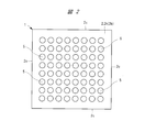
- FIG. 2 is a bottom view of the semiconductor device shown in FIG. 1.
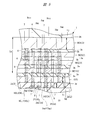
- FIG. 2 is a perspective plan view showing an internal structure of a semiconductor device on a wiring board in a state where a sealing body shown in FIG. 1 is removed.
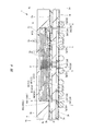
- FIG. 2 is a cross-sectional view taken along line AA in FIG. It is an expanded sectional view of the A section shown in FIG.
- FIG. 5 is a plan view showing the surface side of the memory chip shown in FIG. 4.
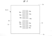
- FIG. 7 is a plan view illustrating an example of a back surface side of the memory chip illustrated in FIG. 6. It is a top view which shows the surface side of the logic chip shown in FIG.
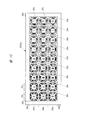
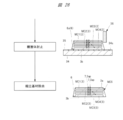
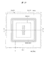
- FIG. 11 is an explanatory diagram showing an outline of a manufacturing process of the semiconductor device described with reference to FIGS. 1 to 10; It is a top view which shows the whole structure of the wiring board prepared by the board
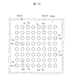
- FIG. 13 is an enlarged plan view for one device region shown in FIG. 12.
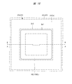
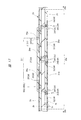
- FIG. 14 is an enlarged sectional view taken along line AA in FIG. 13. It is an enlarged plan view which shows the surface on the opposite side of FIG. It is an enlarged plan view which shows the state which has arrange
- FIG. 17 is an enlarged sectional view taken along line AA in FIG. 16. It is explanatory drawing which shows typically the outline
- FIG. 19 is an explanatory diagram schematically showing an overview of the manufacturing process of the semiconductor chip following FIG. 18.
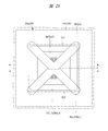
- FIG. 17 is an enlarged plan view showing a state where the logic chip LC is mounted on the chip mounting region of the wiring board shown in FIG. 16.
- FIG. 21 is an enlarged sectional view taken along line AA in FIG. 20. It is explanatory drawing which shows the detailed flow of the 1st chip mounting process shown in FIG. 11, Comprising: It is explanatory drawing which shows typically the state which mounted the semiconductor chip on the chip
- FIG. 21 is an enlarged plan view showing a state in which an adhesive is arranged on the back surface and the periphery of the semiconductor chip shown in FIG. 20.
- FIG. 26 is an enlarged sectional view taken along line AA in FIG. 25.
- FIG. 5 is an explanatory diagram schematically showing an outline of an assembly process of the memory chip stack shown in FIG. 4.
- FIG. 28 is an explanatory diagram schematically showing an outline of a process of assembling a memory chip stack following FIG. 27;
- FIG. 26 is an enlarged plan view showing a state in which a stacked body of memory chips is mounted on the back surface of the logic chip shown in FIG. 25.
- FIG. 30 is an enlarged sectional view taken along line AA in FIG. 29.
- FIG. 31 is an enlarged cross-sectional view showing a state where a sealing body is formed on the wiring substrate shown in FIG. 30 and a plurality of stacked semiconductor chips are sealed. It is a top view which shows the whole structure of the sealing body shown in FIG. It is principal part sectional drawing which shows the state which has arrange
- FIG. 40 is a main part sectional view showing a state in which the wiring board shown in FIG. 39 is taken out from the molding die; FIG.
- FIG. 36 is an enlarged cross-sectional view showing a state in which solder balls are bonded onto a plurality of lands of the wiring board shown in FIG. 35.
- FIG. 42 is a cross-sectional view showing a state in which the multi-piece wiring board shown in FIG. 41 is separated into pieces.
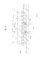
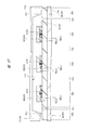
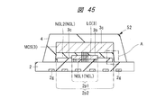
- FIG. 5 is a main part sectional view showing an outline of a modification of the semiconductor device shown in FIG. 4;
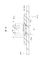
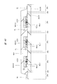
- FIG. 5 is a cross-sectional view of a principal part showing an outline of another modification example of the semiconductor device shown in FIG. 4.
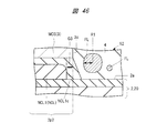
- FIG. 45 is a main part sectional view showing an outline of a modification of the semiconductor device shown in FIG. 44; It is an expanded sectional view of the A section of FIG. FIG.
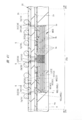
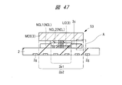
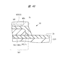
- FIG. 5 is a cross-sectional view of a principal part showing an outline of another modification example of the semiconductor device shown in FIG. 4. It is an expanded sectional view of the A section of FIG.
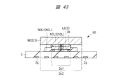
- FIG. 10 is a main part cross-sectional view showing another modification example of the semiconductor device shown in FIG. 4.
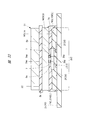
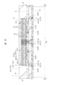
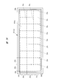
- FIG. 35 is an explanatory view showing a state in which the laminated body is tilted in an examination example different from FIGS. 31 to 34; It is principal part sectional drawing which shows the example of examination with respect to FIG.
- X consisting of A is an element other than A unless specifically stated otherwise and clearly not in context. It does not exclude things that contain.
- the component it means “X containing A as a main component”.
- silicon member is not limited to pure silicon, but includes a SiGe (silicon-germanium) alloy, other multi-component alloys containing silicon as a main component, and other additives. Needless to say, it is also included.
- gold plating, Cu layer, nickel / plating, etc. unless otherwise specified, not only pure materials but also members mainly composed of gold, Cu, nickel, etc. Shall be included.
- hatching or the like may be omitted even in a cross section when it becomes complicated or when it is clearly distinguished from a gap.
- the contour line of the background may be omitted even if the hole is planarly closed.
- hatching or a dot pattern may be added in order to clearly indicate that it is not a void or to clearly indicate the boundary of a region.
- FIG. 1 is a perspective view of the semiconductor device of the present embodiment
- FIG. 2 is a bottom view of the semiconductor device shown in FIG.
- FIG. 3 is a perspective plan view showing the internal structure of the semiconductor device on the wiring board with the sealing body shown in FIG. 1 removed.
- FIG. 4 is a cross-sectional view taken along the line AA in FIG.
- FIGS. 1 to 4 the number of terminals is reduced for the sake of clarity, but the number of terminals (bonding leads 2f, lands 2g, solder balls 5) is shown in FIGS.
- the embodiment is not limited.
- the outline of the logic chip LC is indicated by a dotted line in order to make it easy to see the positional relationship and the planar size difference between the logic chip LC and the memory chip MC4 in plan view.
- the semiconductor device 1 according to the present embodiment includes a wiring substrate 2, a plurality of semiconductor chips 3 (see FIG. 4) mounted on the wiring substrate 2, and a sealing body (resin body) 4 that seals the plurality of semiconductor chips 3. Is provided.
- the wiring board 2 includes an upper surface (surface, main surface, chip mounting surface) 2a on which a plurality of semiconductor chips 3 are mounted, and a lower surface (surface, main surface, mounting surface) opposite to the upper surface 2a. ) 2b and a side surface 2c disposed between the upper surface 2a and the lower surface 2b, and forms a rectangular outer shape in plan view as shown in FIGS.
- the planar size of the wiring board 2 is, for example, a square having a side length of about 14 mm.
- the thickness (height) of the wiring board 2, that is, the distance from the upper surface 2a to the lower surface 2b shown in FIG. 4 is, for example, about 0.3 mm to 0.5 mm.
- the wiring substrate 2 is an interposer for electrically connecting the semiconductor chip 3 mounted on the upper surface 2a side and a mounting substrate (not shown), and a plurality of wiring layers electrically connecting the upper surface 2a side and the lower surface 2b side. (4 layers in the example shown in FIG. 4).
- an insulating layer (core layer) 2e that insulates between the plurality of wirings 2d and the plurality of wirings 2d and between adjacent wiring layers is formed.
- the wiring 2d includes a wiring 2d1 formed on the upper surface or the lower surface of the insulating layer 2e, and a via wiring 2d2 that is an interlayer conductive path formed so as to penetrate the insulating layer 2e in the thickness direction.
- a plurality of bonding leads (terminals, chip mounting surface side terminals, electrodes) 2 f which are terminals electrically connected to the semiconductor chip 3 are formed on the upper surface 2 a of the wiring board 2.
- a plurality of lands 2g, to which a plurality of solder balls 5 which are terminals for electrical connection to a mounting board (not shown), that is, external connection terminals of the semiconductor device 1, are joined. Is formed.
- the plurality of bonding leads 2f and the plurality of lands 2g are electrically connected to each other via a plurality of wirings 2d.
- the bonding lead 2f and the land 2g are shown as a part of the wiring 2d. Yes.
- the upper surface 2a and the lower surface 2b of the wiring board 2 are covered with insulating films (solder resist films) 2h and 2k.
- the wiring 2d formed on the upper surface 2a of the wiring board 2 is covered with an insulating film 2h.
- An opening is formed in the insulating film 2h, and at least a part of the plurality of bonding leads 2f (bonding portions and bonding regions with the semiconductor chip 3) is exposed from the insulating film 2h in the opening.
- the wiring 2d formed on the lower surface 2b of the wiring board 2 is covered with an insulating film 2k.
- An opening is formed in the insulating film 2k, and at least a part of the plurality of lands 2g (joined portions with the solder balls 5) is exposed from the insulating film 2k in the opening.
- a plurality of solder balls (external terminals, electrodes, external electrodes) 5 bonded to a plurality of lands 2g on the lower surface 2b of the wiring board 2 are arranged in a matrix (array) as shown in FIG. Are arranged in a matrix).
- a plurality of lands 2g (see FIG. 4) to which a plurality of solder balls 5 are joined are also arranged in a matrix (matrix).
- a semiconductor device in which a plurality of external terminals (solder balls 5 and lands 2g) are arranged in a matrix on the mounting surface side of the wiring board 2 is referred to as an area array type semiconductor device.
- the mounting surface (lower surface 2b) side of the wiring board 2 can be effectively used as an arrangement space for external terminals. Therefore, even if the number of external terminals increases, the mounting area of the semiconductor device increases. It is preferable at the point which can suppress. That is, a semiconductor device in which the number of external terminals increases with higher functionality and higher integration can be mounted in a space-saving manner.
- the semiconductor device 1 includes a plurality of semiconductor chips 3 mounted on the wiring board 2.
- the plurality of semiconductor chips 3 are stacked on the upper surface 2 a of the wiring board 2.
- Each of the plurality of semiconductor chips 3 includes a front surface (main surface, upper surface) 3a, a back surface (main surface, lower surface) 3b opposite to the surface 3a, and a side surface located between the front surface 3a and the back surface 3b. 3c, and has a rectangular outer shape in plan view as shown in FIG.
- the mounting area can be reduced even when the function of the semiconductor device 1 is enhanced.
- the semiconductor chip 3 mounted in the lowest stage is a logic chip (semiconductor chip) LC in which an arithmetic processing circuit is formed.
- the semiconductor chip 3 mounted on the upper stage of the logic chip is a memory chip (semiconductor chip) MC1, MC2, in which a main memory circuit (memory circuit) for storing data communicated with the logic chip LC is formed.
- MC3 and MC4 The logic chip LC is formed with a control circuit for controlling the operation of the main memory circuits of the memory chips MC1, MC2, MC3, and MC4 in addition to the arithmetic processing circuit described above.
- the logic chip LC is formed with a memory circuit having a smaller capacity than the main memory circuit, such as a cache memory.
- the logic chip LC is formed with an external interface circuit that inputs and outputs signals with an external device (not shown).
- the logic chip LC is formed with an internal interface circuit for inputting / outputting signals to / from internal devices (for example, memory chips MC1, MC2, MC3, MC4).
- a circuit in which circuits necessary for the operation of a certain device or system are formed on a single semiconductor chip 3 like a logic chip LC is called a SoC (System on a Chip).
- SoC System on a Chip
- SIP System In Package
- the required capacity of the main memory circuit varies depending on the device or system to be operated.
- the memory chips MC1, MC2, MC3, and MC4 including the main memory circuit are mounted separately from the logic chip LC that is the SoC, and the logic chip LC and the memory chips MC1, MC2, and MC3 are mounted.
- MC4 are electrically connected.
- FIG. 4 shows an example in which four memory chips MC1, MC2, MC3, and MC4 are stacked on one logic chip LC, but there are various modifications to the number of stacked semiconductor chips 3.
- the minimum configuration can be applied to a modification in which one memory chip MC1 is mounted on one logic chip LC.
- a method for electrically connecting the logic chip LC and the memory chips MC1, MC2, MC3, and MC4 will be described in detail later.
- the logic chip LC can reduce the planar size by improving the integration degree of circuit elements.
- the capacity of the main memory circuit and the transmission speed for example, the data transfer amount depending on the width of the data bus
- the planar size of the memory chip MC4 is larger than the planar size of the logic chip LC.
- the planar size of the memory chip MC4 is a rectangle with a side length of about 8 mm to 10 mm
- the planar size of the logic chip LC is a rectangle with a side length of about 5 mm to 6 mm.
- the planar size of the memory chips MC1, MC2, and MC3 shown in FIG. 4 is the same as the planar size of the memory chip MC4.
- the logic chip LC is formed with an external interface circuit that inputs and outputs signals to and from an external device (not shown), so that a plurality of transmission distances from the external device can be reduced.
- the stacking order of the semiconductor chips 3 is preferably such that the logic chip LC is mounted at the lowest stage, that is, at a position closest to the wiring board 2. That is, the semiconductor chip 3 (memory chips MC1, MC2, MC3, MC4) having a large planar size is stacked on the semiconductor chip 3 (logic chip LC) having a small planar size as in the semiconductor device 1. For this reason, as shown in FIG. 4, in the region outside the peripheral edge of the lowermost semiconductor chip 3 (logic chip LC), the upper semiconductor chip 3 (memory chip MC1) and the upper surface 2a of the wiring board 2 are located. There is a gap in
- an adhesive (insulating adhesive) NCL is disposed between the upper semiconductor chip 3 (memory chip MC1) and the upper surface 2a of the wiring board 2 so as to fill this gap.
- the adhesive NCL includes an adhesive (insulating adhesive) NCL1 for bonding and fixing the logic chip LC on the wiring board 2, and an adhesive (insulating adhesive) NCL2 for bonding and fixing the memory chip MC1 on the logic chip LC.
- the peripheral portion of the adhesive material NCL1, in particular, the side surface (surface aligned with the side surface of the logic chip LC) is covered with the adhesive material NCL2.
- the adhesive NCL2 has a fillet formed so as to cover the side surface of the memory chip (at least the memory chip MC1). Further, a part of the fillet of the adhesive material NCL2 is formed on the outer side (direction away from the logic chip LC) than the peripheral edge (side surface) of the memory chip.
- the adhesive materials NCL1 and NCL2 are each made of an insulating (non-conductive) material (for example, a resin material).
- a sealing body different from the sealing body 4 (chip stacking body sealing body, chip stacking body resin body) ) 6 is arranged, and the stacked body MCS of the memory chips MC1, MC2, MC3, and MC4 is sealed by the sealing body 6.
- the sealing body 6 is embedded so as to be in close contact with the front surface 3a and the back surface 3b of the plurality of memory chips MC1, MC2, MC3, and MC4, and the stacked body MCS of the memory chips MC1, MC2, MC3, and MC4 includes each semiconductor chip 3. It is integrated by the joint part between them and the sealing body 6.
- the sealing body 6 is made of an insulating (non-conductive) material (for example, a resin material), and the sealing body 6 is disposed at each joint portion of the memory chips MC1, MC2, MC3, and MC4.
- a plurality of electrodes provided at the joint can be electrically insulated.
- the surface 4a of the memory chip MC1 mounted at the lowest stage (position closest to the logic chip LC) is a sealing body. 6 is exposed. As shown in FIGS.
- the semiconductor device 1 includes a sealing body 4 that seals the plurality of semiconductor chips 3.
- the sealing body 4 includes an upper surface (surface, front surface) 4a, a lower surface (surface, rear surface) 4b (see FIG. 4) positioned on the opposite side of the upper surface 4a, and a side surface 4c positioned between the upper surface 4a and the lower surface 4b. And has a rectangular outer shape in plan view.
- the planar size of the sealing body 4 (the dimension when viewed in plan from the upper surface 4 a side, the outer size of the upper surface 4 a) is the same as the planar size of the wiring board 2.
- the side surface 4 c is continuous with the side surface 2 c of the wiring board 2.
- the planar dimension (dimension in planar view) of the sealing body 4 comprises a square whose length of one side is about 14 mm, for example.
- the sealing body 4 is a resin body that protects the plurality of semiconductor chips 3.
- the sealing body 4 is formed between the semiconductor chips 3 and between the semiconductor chips 3 and the wiring substrate 2, thereby forming a thin semiconductor. Damage to the chip 3 can be suppressed.
- the sealing body 4 is comprised with the following materials from a viewpoint of improving the function as a protection member, for example.
- the sealing body 4 is easily adhered to the semiconductor chip 3 and the wiring substrate 2 and is required to have a certain degree of hardness after sealing, and therefore includes, for example, a thermosetting resin such as an epoxy resin. It is preferable.
- filler particles such as silica (silicon dioxide; SiO 2 ) particles are preferably mixed in the resin material.
- the mixing ratio of the filler particles is adjusted to bring the linear expansion coefficients of the semiconductor chip 3 and the sealing body 4 closer. It is preferable.
- FIG. 5 is an enlarged cross-sectional view of a portion A shown in FIG. 6 is a plan view showing the front surface side of the memory chip shown in FIG. 4, and FIG. 7 is a plan view showing an example of the back surface side of the memory chip shown in FIG. 8 is a plan view showing the front surface side of the logic chip shown in FIG. 4, and FIG. 9 is a plan view showing an example of the back surface side of the logic chip shown in FIG.
- FIG. 10 is an enlarged sectional view of a portion B in FIG.
- FIGS. 7 shows a back view of the memory chips MC1, MC2, and MC3, the structure of the back surface of the memory chip MC4 (see FIG. 4) where the back electrode 3bp is not formed is shown in FIG. Is omitted.
- the inventor of the present application is examining a technique for improving the performance of the SIP type semiconductor device.
- the signal transmission speed between a plurality of semiconductor chips mounted on the SIP is set to 12 Gbps (12 gigabits per second), for example.
- the technology to be improved was examined.
- As a method for improving the transmission speed between a plurality of semiconductor chips mounted on the SIP there is a method of increasing the data bus width of the internal interface and increasing the amount of data transmitted at one time (hereinafter referred to as bus width expansion). ).
- bus width expansion As another method, there is a method of increasing the number of transmissions per unit time (hereinafter referred to as high clock).
- the semiconductor device 1 described with reference to FIGS. 1 to 4 is a semiconductor device in which the transmission speed of the internal interface is improved to 12 Gbps or more by applying a combination of bus width expansion and high clock.
- the memory chips MC1, MC2, MC3, and MC4 shown in FIG. 4 are so-called wide I / O memories each having a 512-bit data bus width.
- each of the memory chips MC1, MC2, MC3, and MC4 includes four channels each having a data bus width of 128 bits, and the total bus width of these four channels is 512 bits.
- the number of transmissions per unit time of each channel is increased to, for example, 3 Gbps or more.
- the logic chip LC and the memory chip MC1 are electrically connected via a conductive member disposed between the logic chip LC and the memory chip MC1.
- the plurality of memory chips MC1, MC2, MC3, and MC4 are electrically connected to each other through conductive members disposed between the plurality of memory chips MC1, MC2, MC3, and MC4.
- the transmission path between the logic chip LC and the memory chip MC1 does not include the wiring substrate 2 or a wire (bonding wire) (not shown). Further, in the semiconductor device 1, the transmission path between the plurality of memory chips MC1, MC2, MC3, and MC4 does not include the wiring board 2 or wires (not shown) (bonding wires).
- the logic chip LC has a plurality of front surface electrodes (electrodes, pads) 3ap formed on the front surface 3a and a plurality of back surface electrodes (electrodes, pads) 3bp formed on the back surface 3b.
- the logic chip LC is formed so as to penetrate from one of the front surface 3a and the back surface 3b toward the other, and a plurality of through electrodes that electrically connect the plurality of front surface electrodes 3ap and the plurality of back surface electrodes 3bp. It has an electrode 3tsv.
- the semiconductor chip 3 includes a semiconductor substrate (not shown) made of, for example, silicon (Si), and a plurality of semiconductor elements (not shown) such as transistors are provided on the main surface (element forming surface) of the semiconductor substrate. Is formed.
- a wiring layer (not shown) including a plurality of wirings and an insulating film that insulates between the plurality of wirings is stacked on the main surface (front surface 3a side) of the semiconductor substrate.
- a plurality of wirings in the wiring layer are electrically connected to a plurality of semiconductor elements, respectively, to constitute a circuit.
- a plurality of surface electrodes 3ap formed on the surface 3a (see FIG. 3) of the semiconductor chip 3 are electrically connected to the semiconductor element through a wiring layer provided between the semiconductor substrate and the surface 3a, and Part of it.
- the back electrode by forming the through electrode 3tsv penetrating the semiconductor chip 3 in the thickness direction and electrically connecting the front electrode 3ap and the back electrode 3bp via the through electrode 3tsv, the back electrode
- the circuit of the semiconductor chip 3 formed on the side of 3 bp and the surface 3a can be electrically connected. That is, as shown in FIG. 5, the front surface electrode 3ap of the memory chip MC1 and the back surface electrode 3bp of the logic chip LC are electrically connected via a conductive member such as a protruding electrode (conductive member, bump electrode) 7.
- the circuit of the memory chip MC1 and the circuit of the logic chip LC are electrically connected through the through electrode 3tsv.
- the logic chip LC mounted between the memory chip MC1 and the wiring board 2 has a plurality of through electrodes 3tsv. For this reason, by electrically connecting the memory chip MC1 and the logic chip LC via the through electrode 3tsv, the wiring substrate 2 and a wire (not shown) (bonding wire) are connected from the transmission path between the logic chip LC and the memory chip MC1. ) Can be eliminated. As a result, the impedance component in the transmission path between the logic chip LC and the memory chip MC1 can be reduced, and the influence of noise due to the high clock can be reduced. In other words, even when the signal transmission speed between the logic chip LC and the memory chip MC1 is improved, the transmission reliability can be improved.
- the semiconductor chips 3 are arranged above and below among the plurality of memory chips MC1, MC2, MC3, MC4.
- the memory chips MC1, MC2, and MC3 have a plurality of through electrodes 3tsv, like the logic chip LC.
- each of the memory chips MC1, MC2, and MC3 has a plurality of front surface electrodes (electrodes and pads) 3ap formed on the front surface 3a and a plurality of back surface electrodes (electrodes and pads) 3bp formed on the back surface 3b. is doing.
- Each of the memory chips MC1, MC2, and MC3 is formed so as to penetrate from one of the front surface 3a and the back surface 3b toward the other, and electrically connects the plurality of front surface electrodes 3ap and the plurality of back surface electrodes 3bp.
- a plurality of through-electrodes 3tsv connected to.
- the surface electrode 3ap of the upper semiconductor chip 3 and the back electrode 3bp of the lower semiconductor chip 3 are connected to the protruding electrodes. If electrically connected via a conductive member such as (conductive member, bump electrode) 7, the circuits of the plurality of stacked semiconductor chips 3 are electrically connected via the through electrode 3tsv.
- the wiring board 2 and wires (not shown) (bonding wires) can be excluded from the transmission path between the memory chips MC1, MC2, MC3, and MC4.
- the impedance component in the transmission path between the plurality of stacked memory chips MC1, MC2, MC3, and MC4 and to reduce the influence of noise caused by increasing the clock.
- the transmission reliability can be improved.
- the memory chip MC4 mounted on the uppermost layer only needs to be connected to the memory chip MC3. Therefore, a plurality of front surface electrodes 3ap are formed, but a plurality of back surface electrodes 3bp and a plurality of back surface electrodes 3bp are formed.
- the through electrode 3tsv is not formed.
- the memory chip MC4 mounted in the uppermost stage adopts a structure that does not include the plurality of back surface electrodes 3bp and the plurality of through electrodes 3tsv, thereby simplifying the manufacturing process of the memory chip MC4.
- the memory chip MC4 can also have a structure including a plurality of back surface electrodes 3bp and a plurality of through electrodes 3tsv, similarly to the memory chips MC1, MC2, and MC3. .
- manufacturing efficiency can be improved by making the plurality of stacked memory chips MC1, MC2, MC3, and MC4 have the same structure.
- the protruding electrode 7 disposed between the stacked semiconductor chips 3 and electrically connecting the surface electrode 3ap of the upper semiconductor chip 3 and 3 bp of the lower semiconductor chip 3
- the protruding electrode 7 is a metal member in which a nickel (Ni) film and a solder (for example, SnAg) film are stacked on the tip of a member mainly composed of copper (Cu) formed in a columnar shape (for example, a columnar shape). Electrical connection is established by bonding the solder film at the tip to the back electrode 3bp.
- a solder material can be joined to the exposed surface of the surface electrode 3ap, and this solder material can be used as the protruding electrode 7.
- the semiconductor chip 3 including the through electrode 3tsv has a small thickness (ie, a separation distance between the front surface 3a and the back surface 3b). It is preferable. If the thickness of the semiconductor chip 3 is reduced, the transmission distance of the through electrode 3tsv is shortened, which is preferable in that the impedance component can be reduced. Further, when an opening (including a through hole and a hole that does not penetrate) is formed in the thickness direction of the semiconductor substrate, the processing accuracy decreases as the depth of the hole increases. In other words, if the thickness of the semiconductor chip 3 is reduced, the processing accuracy of the opening for forming the through electrode 3tsv can be improved. For this reason, since the diameters (length and width in the direction orthogonal to the thickness direction of the semiconductor chip 3) of the plurality of through electrodes 3tsv can be made uniform, the impedance components of the plurality of transmission paths can be easily controlled.
- the thickness T1 of the logic chip LC is larger than the thickness TA of the stacked body MCS (see FIG. 4) of the plurality of memory chips MC1, MC2, MC3, and MC4 arranged on the logic chip LC. thin.
- the thickness T1 of the logic chip LC is thinner than the thickness T2 of the memory chip MC4 that is mounted at the top of the plurality of memory chips MC1, MC2, MC3, and MC4 and does not have the through electrode 3tsv.
- the thickness T1 of the logic chip LC is 50 ⁇ m.
- the thickness of the memory chip MC4 is about 80 ⁇ m to 100 ⁇ m.
- the thickness TA of the stacked body MCS (see FIG. 4) of the plurality of memory chips MC1, MC2, MC3, and MC4 is about 260 ⁇ m.
- the sealing body 4 is brought into close contact with the plurality of semiconductor chips 3 and sealed. For this reason, the sealing body 4 functions as a protective member for the semiconductor chip 3 and can suppress damage to the semiconductor chip 3. That is, according to the present embodiment, the reliability (durability) of the semiconductor device 1 can be improved by sealing the plurality of semiconductor chips 3 with resin.
- the gap G1 between the surface 3a of the logic chip LC and the upper surface 2a of the wiring board 2 is, for example, about 10 ⁇ m to 20 ⁇ m.
- a gap G2 between the surface 3a of the memory chip MC1 and the upper surface 2a of the wiring board 2 is, for example, about 70 ⁇ m to 100 ⁇ m.
- the plurality of surface electrodes 3ap included in the memory chips MC1, MC2, MC3, and MC4 are arranged in a central portion on the surface 3a.
- the plurality of surface electrodes 3ap included in the memory chips MC1, MC2, and MC3 are arranged in a central portion on the surface 3a.
- the plurality of front surface electrodes 3ap of the memory chips MC1, MC2, MC3, and MC4 and the plurality of back surface electrodes 3bp of the memory chips MC1, MC2, and MC3 are arranged at positions that overlap each other in the thickness direction. Yes.
- a part (a plurality of surface electrodes 3ap1) of the plurality of surface electrodes 3ap included in the logic chip LC is collectively arranged in the central portion on the surface 3a.
- a part (a plurality of surface electrodes 3ap2) of the plurality of surface electrodes 3ap included in the logic chip LC is disposed along the side (side surface 3c) of the surface 3a at the peripheral edge of the surface 3a.
- the plurality of surface electrodes 3ap1 arranged at the center of the surface 3a are electrically connected to the back electrode 3bp via the through electrode 3tcv shown in FIG.
- the plurality of surface electrodes 3ap1 are internal interface electrodes.
- the plurality of surface electrodes 3ap2 arranged at the periphery of the surface 3a are electrically connected to an external device (not shown) via the wiring board 2 shown in FIG. ing.
- the surface electrode 3ap2 is electrically bonded to the bonding lead 2f via the protruding electrode 7 and the bonding material 8 such as solder. That is, the plurality of surface electrodes 3ap2 are electrodes for external interfaces.
- the front surface electrode 3ap and the back surface electrode 3bp for the internal interface are arranged at positions overlapping in the thickness direction, and the protruding electrodes 7 are interposed.
- the connection method is particularly preferable.
- the planar size of the logic chip LC is smaller than the planar size of the memory chips MC1, MC2, MC3, and MC4.
- the central portion (central region) of the back surface 3b of the logic chip LC is arranged so as to overlap the central portion (central region) of the memory chip MC4 in plan view. That is, in plan view, the four side surfaces 3c of the memory chip MC4 are disposed outside the four side surfaces 3c of the logic chip LC.
- the plurality of semiconductor chips 3 are arranged on the wiring substrate 2 such that the four side surfaces 3c of the memory chip MC4 are located between the four side surfaces 3c of the logic chip LC and the four side surfaces 2c of the wiring substrate 2. Stacked and mounted.
- the memory chips MC1, MC2, and MC3 shown in FIG. 4 are arranged at positions (the same positions) that overlap with the memory chip MC4 in a plan view.
- peripheral portions of the memory chips MC1, MC2, MC3, and MC4 are arranged in a position overlapping the peripheral region outside the logic chip LC in plan view.
- the logic chip LC does not exist between the peripheral portions of the memory chips MC1, MC2, MC3, and MC4 and the wiring board 2 (see, for example, FIG. 10).
- the surface electrode 3ap and the back surface electrode 3bp for the internal interface of each semiconductor chip 3 shown in FIG. 5 are the surface electrode 3ap and the back surface electrode 3bp for the internal interface of each semiconductor chip 3 shown in FIG. 5 so as to overlap in the thickness direction.
- the logic chip LC is preferably arranged at a position overlapping the thickness direction.
- a plurality of surface electrodes 3ap2 for external interface are arranged on the peripheral edge of the logic chip LC. Therefore, on the surface 3a of the logic chip LC, it is preferable that the plurality of surface electrodes 3ap1 for the internal interface are collectively arranged at the center of the surface 3a.
- a plurality of memory regions (memory circuit element array regions) MR are formed on the surface 3a side (specifically, on the main surface of the semiconductor substrate) of the memory chips MC1, MC2, MC3, and MC4.
- four memory regions MR corresponding to the above-described four channels are formed.
- a plurality of memory cells (storage circuit elements) are arranged in an array in each memory region MR.
- the memory region MR for four channels is formed so as to surround the region where the surface electrode group is arranged. Can be placed.
- the distance from each memory region MR to the surface electrode 3ap can be equalized.
- the transmission distance of each of the plurality of channels can be made equal, which is preferable in that an error in transmission speed for each channel can be reduced.
- the surface electrode 3ap1 concentrated at the center of the surface 3a of the logic chip LC shown in FIG. 8 is used as an electrode exclusively for the internal interface
- the surface electrode 3ap1 is electrically connected to the wiring board 2 shown in FIG. It can function without being connected.
- a part of the surface electrode 3ap1 when a part of the surface electrode 3ap1 is electrically connected to the bonding lead 2f of the wiring board 2, a part of the surface electrode 3ap1 can be used as an electrode for an external interface. preferable.
- a drive circuit for driving a memory circuit (not shown) is formed in the memory chips MC1, MC2, MC3, and MC4.
- the drive circuit has a power supply potential (first reference potential) and a reference potential (first reference potential). It is conceivable to use a part of the surface electrode 3ap1 as a terminal for supplying a second reference potential different from the reference potential (for example, a ground potential).
- first reference potential a power supply potential
- first reference potential first reference potential
- first reference potential first reference potential
- a part of the surface electrode 3ap1 it is preferable to shorten the transmission distance between the power supply source and the circuit that consumes the power from the viewpoint of suppressing the instability of operation due to an instantaneous voltage drop or the like.
- the distance to the drive circuits of the memory chips MC1, MC2, MC3, MC4 on which the circuit that consumes the power is formed can be shortened. This is preferable.
- FIG. 11 is an explanatory diagram showing an outline of the manufacturing process of the semiconductor device described with reference to FIGS. Details of each step will be described below with reference to FIGS.
- FIGS. 12 to 15 are plan views showing the entire structure of the wiring board prepared in the board preparation step shown in FIG. 11, and FIG. 13 is an enlarged plan view for one device region shown in FIG.
- FIG. 14 is an enlarged sectional view taken along line AA in FIG.
- FIG. 15 is an enlarged plan view showing the opposite surface of FIG.
- the number of terminals is reduced for the sake of clarity, but the number of terminals (bonding leads 2f, lands 2g) is limited to the mode shown in FIGS. Not.
- the wiring board 20 prepared in this step includes a plurality of device regions 20a inside a frame portion (outer frame) 20b. Specifically, a plurality (27 in FIG. 12) of device regions 20a are arranged in a matrix. Each of the plurality of device regions 20a corresponds to the wiring board 2 shown in FIGS.
- the wiring substrate 20 is a so-called multi-piece substrate having a plurality of device regions 20a and dicing lines (dicing regions) 20c between the device regions 20a.
- manufacturing efficiency can be improved by using a multi-piece substrate provided with a plurality of device regions 20a.
- the wiring board 20 has an upper surface 2a, a lower surface 2b opposite to the upper surface 2a, and a plurality of wiring layers (four layers in the example shown in FIG. 4) that electrically connect the upper surface 2a side and the lower surface 2b side.
- an insulating layer (core layer) 2e that insulates between the plurality of wirings 2d and the plurality of wirings 2d and between adjacent wiring layers is formed.
- the wiring 2d includes a wiring 2d1 formed on the upper surface or the lower surface of the insulating layer 2e, and a via wiring 2d2 that is an interlayer conductive path formed so as to penetrate the insulating layer 2e in the thickness direction.
- the upper surface 2a of the wiring substrate 20 is a chip mounting area (chip mounting portion) which is a planned area for mounting the logic chip LC shown in FIG. 8 in the first chip mounting process shown in FIG. 2p1 is included.
- the chip mounting area 2p1 is present at the center of the device area 20a on the upper surface 2a.
- the outline of the chip mounting area is indicated by a two-dot chain line in order to show the position of the chip mounting area 2p1, but the chip mounting area 2p1 is actually a region to be mounted with the logic chip LC as described above. There need not be possible borders.
- a plurality of bonding leads (terminals, chip mounting surface side terminals, electrodes) 2f are formed on the upper surface 2a of the wiring board 20.
- the bonding lead 2f is a terminal electrically connected to the plurality of surface electrodes 3ap formed on the surface 3a of the logic chip LC shown in FIG. 8 in the first chip mounting step shown in FIG.
- the bonding portions of the plurality of bonding leads 2f are connected to the chip. It is formed inside the mounting region 2p1.
- the upper surface 2a of the wiring board 20 is covered with an insulating film (solder resist film) 2h.
- An opening 2hw is formed in the insulating film 2h, and at least a part of the plurality of bonding leads 2f (bonding portion with semiconductor chip, bonding region) is exposed from the insulating film 2h in the opening 2hw.
- a plurality of lands 2 g are formed on the lower surface 2 b of the wiring board 20.
- the lower surface 2b of the wiring board 20 is covered with an insulating film (solder resist film) 2k.
- An opening 2kw is formed in the insulating film 2k, and at least a part of the plurality of lands 2g (joined portions with the solder balls 5) is exposed from the insulating film 2k in the opening 2kw.
- the plurality of bonding leads 2f and the plurality of lands 2g are electrically connected to each other via a plurality of wirings 2d.
- the conductor patterns such as the plurality of wirings 2d, the plurality of bonding leads 2f, and the plurality of lands 2g are formed of a metal material containing copper (Cu) as a main component, for example.
- the plurality of wirings 2d, the plurality of bonding leads 2f, and the plurality of lands 2g can be formed by, for example, an electrolytic plating method.
- the wiring board 20 having four or more wiring layers (four layers in FIG. 14) can be formed by, for example, a build-up method.
- FIG. 16 is an enlarged plan view showing a state in which an adhesive is disposed in the chip mounting area shown in FIG. 13, and FIG. 17 is an enlarged cross-sectional view taken along the line AA in FIG.
- the outlines of the chip mounting areas 2p1 and 2p2 are indicated by two-dot chain lines in order to show the positions of the chip mounting area 2p1 and the chip mounting area 2p2, but the chip mounting areas 2p1 and 2p2 are respectively logic chip LC.
- a method of sealing the connecting portion with a resin after electrically connecting the semiconductor chip and the wiring substrate Is performed.
- the resin is supplied from a nozzle disposed in the vicinity of the gap between the semiconductor chip and the wiring board, and the resin is embedded in the gap using a capillary phenomenon.
- the adhesive NCL1 is disposed in the chip mounting region 2p1, and the adhesive NCL1
- the logic chip LC is mounted by a method (first coating method) in which the logic chip LC is pressed from above and electrically connected to the wiring substrate 20.
- the processing time (the time for injecting the resin) for one device region 20a becomes long.
- the tip of the logic chip LC for example, the solder material formed at the tip of the protruding electrode 7 shown in FIGS. 5 and 10.
- the bonding portion of the bonding lead 2f contact each other, An adhesive NCL1 has already been embedded between the wiring board 20 and the logic chip LC. Therefore, it is preferable in that the processing time for one device region 20a can be shortened and the manufacturing efficiency can be improved as compared with the above-described post-injection method.
- the adhesive NCL1 used in the pre-coating method is made of an insulating (non-conductive) material (for example, a resin material).
- the adhesive NCL1 is made of a resin material whose hardness (hardness) is increased (increased) by applying energy, and in the present embodiment, for example, includes a thermosetting resin. Further, the adhesive NCL1 before curing is softer than the protruding electrodes 7 shown in FIGS. 5 and 10, and is deformed by pressing the logic chip LC.
- the adhesive NCL1 before curing is roughly divided into the following two types depending on the handling method.
- One is made of a paste-like resin (insulating material paste) called NCP (Non-Conductive Paste), and is applied to the chip mounting region 2p1 from a nozzle (not shown).
- the other is a method called NCF (Non-Conductive Film), which is made of a resin (insulating material film) previously formed into a film shape, and is transported to the chip mounting region 2p1 in the film state and pasted.
- the step of attaching as in the case of the insulating material film (NCF) is not required, so that the stress applied to the semiconductor chip or the like can be reduced as compared with the case where the insulating material film is used.
- the insulating film (NCF) is used, the shape retaining property is higher than that of the insulating material paste (NCP), so that the range and thickness of the adhesive material NCL1 can be easily controlled.
- an insulating material film formed in a film shape in advance.
- an adhesive material NCL1 that is an insulating film (NCF) is disposed on the chip mounting region 2p1 and pasted so as to be in close contact with the upper surface 2a of the wiring board 20.
- NCP insulating material paste
- the adhesive material NCL1 has a fixing material function for bonding and fixing the logic chip LC (see FIG. 4) and the wiring board 20 in the first chip bonding process shown in FIG. Further, the adhesive material NCL1 has a sealing material function for protecting the bonding portion between the logic chip LC and the wiring substrate 2 by sealing.
- the sealing function includes a stress relaxation function that protects the joint by dispersing and relaxing the stress transmitted to the joint between the logic chip LC and the wiring board 2.
- the adhesive material NCL1 may be disposed so as to wrap around the joint portion between the logic chip LC and the wiring board 2. Therefore, the adhesive material NCL1 is disposed only in a region overlapping the chip mounting region 2p1. It ’s fine. From the viewpoint of improving the function of the fixing material, it is preferable that a part of the adhesive NC1 is in close contact with the side surface 3c of the logic chip LC shown in FIG. 10, but as shown in FIG. However, it is not necessary to extend the outside greatly.
- the adhesive NCL1 is disposed so as to cover a wider area than the chip mounting region 2p1.
- the chip mounting area 2p2 shown in FIG. 16 is a planned area for mounting the stacked body MCS (see FIG. 4) of the memory chips MC1, MC2, MC3, and MC4 (see FIG. 4) in the second chip mounting process shown in FIG.
- the chip mounting area 2p1 is included and the plane size is larger than the chip mounting area 2p1.
- the peripheral portion of the adhesive NCL1 is disposed between the peripheral portion of the chip mounting region 2p1 and the peripheral portion of the chip mounting region 2p2, and close to the peripheral portion of the chip mounting region 2p2. Is done.
- the adhesive material NCL1 is disposed so as to cover the vicinity of the peripheral edge portion of the chip mounting region 2p2. Specifically, in the example illustrated in FIG. 16, the adhesive material NCL1 has substantially the same planar size as the chip mounting region NCL1.
- FIG. 18 is an explanatory view schematically showing an outline of the manufacturing process of the semiconductor chip provided with the through electrode shown in FIG.
- FIG. 19 is an explanatory view schematically showing the outline of the manufacturing process of the semiconductor chip following FIG. 18 and 19, the description will focus on the through electrode 3tsv and the manufacturing method of the back electrode 3p electrically connected to the through electrode 3tsv, and the steps of forming various circuits other than the through electrode 3tsv will be illustrated and described. Is omitted.
- the semiconductor chip manufacturing method shown in FIGS. 18 and 19 can be applied to the manufacturing method of the memory chips MC1, MC2, and MC3 in addition to the logic chip LC shown in FIG.
- a wafer (semiconductor substrate) WH shown in FIG. 18 is prepared.
- the wafer WH is a semiconductor substrate made of, for example, silicon (Si) and has a circular shape in plan view.
- the wafer WH has a surface (main surface, upper surface) WHs which is a semiconductor element formation surface and a back surface (main surface, lower surface) WHb opposite to the surface WHs.
- the thickness of the wafer WH is larger than the thickness of the logic chip LC and the memory chips MC1, MC2, and MC3 shown in FIG. 4, and is about several hundred ⁇ m, for example.
- a hole (hole, opening) 3tsh for forming the through electrode 3tsv shown in FIG. 5 is formed.
- the mask 25 is disposed on the surface WHs of the wafer WH, and the hole 3 tsh is formed by performing an etching process.
- the semiconductor elements of the logic chip LC and the memory chips MC1, MC2, and MC3 shown in FIG. 4 can be formed, for example, after this process and before the next wiring layer forming process.
- a through electrode 3tsv is formed by embedding a metal material such as copper (Cu) in the hole 3tsh.
- a wiring layer forming step a wiring layer (chip wiring layer) 3d is formed on the surface WHs of the wafer WH.
- the plurality of surface electrodes 3ap shown in FIGS. 5 and 10 are formed, and the plurality of through electrodes 3tsv and the plurality of surface electrodes 3ap are electrically connected to each other.
- the semiconductor elements of the logic chip LC and the memory chips MC1, MC2, and MC3 shown in FIG. 4 and the plurality of surface electrodes 3ap shown in FIGS. 5 and 10 are electrically connected through the wiring layer 3d. .
- the semiconductor elements of the logic chip LC and the memory chips MC1, MC2, and MC3 are electrically connected via the wiring layer 3d.
- the protruding electrode 7 is formed on the surface electrode 3ap (see FIGS. 5 and 10). Further, a solder layer 8 a is formed at the tip of the protruding electrode 7. This solder layer 8 a functions as a bonding material when the semiconductor chip 3 shown in FIG. 5 is mounted on the wiring substrate 2 or the lower semiconductor chip 3.
- the back surface polishing step shown in FIG. 19 the back surface WHb (see FIG. 18) side of the wafer WH is polished to reduce the thickness of the wafer WH. Thereby, the back surface 3b of the semiconductor chip 3 shown in FIG. 5 is exposed. In other words, the through electrode 3tsv penetrates the wafer WH in the thickness direction. Further, the plurality of through electrodes 3tsv are exposed from the wafer WH on the back surface 3b of the wafer WH. In the example shown in FIG.
- the polishing jig 28 is supported in a state where the wafer WH is supported by the protective layer 27 that protects the supporting substrate 26 such as a glass plate and the protruding electrode 7 that protects the front surface WHs side. Use and polish.
- a plurality of back electrodes 3 bp are formed on the back surface 3 b and electrically connected to the plurality of through electrodes 3 tsv.
- the wafer WH is divided along a dicing line to obtain a plurality of semiconductor chips 3. Thereafter, inspection is performed as necessary, and the semiconductor chip 3 (logic chip LC and memory chips MC1, MC2, MC3) shown in FIG. 4 is obtained.
- FIG. 20 is an enlarged plan view showing a state where the logic chip LC is mounted on the chip mounting region of the wiring board shown in FIG.
- FIG. 21 is an enlarged sectional view taken along the line AA in FIG. 22 to 24 are explanatory diagrams showing a detailed flow of the first chip mounting step shown in FIG.
- FIG. 22 is an explanatory view schematically showing a state in which a semiconductor chip is placed on the chip mounting area.
- FIG. 23 is an explanatory view showing a state in which the transport jig shown in FIG. 22 is removed and the heating jig is pressed against the back surface side of the semiconductor chip.
- FIG. 24 is an explanatory view showing a state in which the semiconductor chip is heated and electrically connected to the wiring board.
- the logic chip LC is mounted by a so-called face-down mounting method (flip chip connection method) so that the surface 3a of the logic chip LC faces the upper surface 2a of the wiring board 2.
- the logic chip LC and the wiring board 2 are electrically connected by this process.
- the plurality of surface electrodes 3ap formed on the surface of the logic chip LC and the plurality of bonding leads 2f formed on the upper surface 2a of the wiring board 2 are formed by the protruding electrodes 7 and the bonding material 8 (see FIGS. 5 and 10). It is electrically connected via.
- FIGS. 5 and 10 bonding material
- the logic chip LC semiconductor chip 3
- the logic chip LC is transported onto the chip mounting region 2p1 with the back surface 3b side held by the holding jig 30, and is disposed on the bonding material NCL1 so that the front surface 3a faces the top surface 2a of the wiring board 20.
- the holding jig 30 has a holding surface 30a that holds the back surface 3b of the logic chip LC by suction, and conveys the logic chip LC while being held by the holding surface 30a.
- a protruding electrode 7 is formed on the surface 3 a side of the logic chip LC, and a solder layer 8 a is formed at the tip of the protruding electrode 7.
- a solder layer 8b which is a bonding material for electrically connecting to the protruding electrode 7, is formed at the bonding portion of the bonding lead 2f formed on the upper surface 2a of the wiring board 20.
- the heating jig 31 is pressed against the back surface 3 b side of the logic chip LC, and the logic chip LC is pressed toward the wiring substrate 20.
- the adhesive material NCL1 is in a soft state before being cured. Therefore, when the logic chip LC is pushed in by the heating jig 31, the logic chip LC approaches the wiring board 20.
- the tips of the plurality of protruding electrodes 7 specifically, the solder layer 8a
- the bonding region specifically, the solder layer 8b
- the thickness of the adhesive NCL1 (distance between the upper surface NCL1a and the lower surface NCL1b) is at least the height of the protruding electrode 7 (projection height), the thickness of the bonding lead 2f, and the bonding material (solder layers 8a and 8b). Thicker than the total thickness. For this reason, when it is pushed into the heating jig 31, a part on the surface 3a side of the logic chip LC is embedded in the adhesive NCL1. In other words, at least a part of the side surface 3c of the logic chip LC on the surface 3a side is embedded in the adhesive material NCL1.
- the adhesive NCL1 may be embedded between the logic chip LC and the wiring board 20, but a part of the surface 3a side of the logic chip LC is bonded to the logic chip LC.
- a semiconductor chip By embedding in NCL1, a semiconductor chip can be stably mounted in a second chip mounting step described later. Details will be described in the second chip mounting step.
- a member (low elastic member) softer than the heating jig 31 and the logic chip LC such as a resin film (film) 32, is interposed between the heating jig 31 and the logic chip LC. It is preferable to cover the back surface 3b of the logic chip LC with the resin film 32. If the logic chip LC is pressed through the resin film 32, the resin film 32 adheres to the back surface 3b of the logic chip LC.
- the adhesive material NCL1 remains on the back surface of the logic chip LC. It can suppress going around to 3b.
- the upper surface NCL1a of the adhesive material NCL1 can be planarized by covering the entire region where the adhesive material NCL1 is disposed with the resin film 32.
- the resin film 32 of this Embodiment consists of a fluororesin, for example.
- FIG. 23 shows the state in which the resin film 32 bites into the logic chip LC in an easy-to-understand manner.
- the bonding is performed. It is possible to suppress the material NCL1 from entering the back surface 3b of the logic chip LC.
- the logic chip LC and the adhesive material NCL1 are heated by the heating jig (heat source) 31 in a state where the logic chip LC is pressed against the heating jig 31 as shown in FIG.
- the solder layers 8a and 8b shown in FIG. 23 are respectively melted and integrated to form a joint material (solder material) 8 shown in FIG. That is, by heating the logic chip LC with the heating jig (heat source) 31, the protruding electrode 7 and the bonding lead 2 f are electrically connected through the bonding material 8.
- the adhesive material NCL1 is cured by heating the adhesive material NCL1 with the heating jig (heat source) 31 shown in FIG. As a result, the adhesive NCL1 cured in a state where a part of the logic chip LC is embedded is obtained. Further, since the back surface electrode 3bp of the logic chip LC is covered with the resin film 32, it is exposed from the cured adhesive material NCL1. Note that it is not necessary to completely cure the adhesive material NCL1 by the heat from the heating jig (heat source) 31, and a part of the thermosetting resin contained in the adhesive material NCL1 is cured (temporarily) to such an extent that the logic chip LC can be fixed.
- the wiring board 20 can be transferred to a heating furnace (not shown), and the remaining thermosetting resin can be cured (mainly cured). Although it takes time to complete the main curing process in which the entire thermosetting resin component contained in the adhesive NCL1 is cured, the manufacturing efficiency can be improved by performing the main curing process in a heating furnace.
- FIG. 25 is an enlarged plan view showing a state in which an adhesive is disposed on the back surface and the periphery of the semiconductor chip shown in FIG. 20, and FIG. 26 is an enlarged cross-sectional view along the line AA in FIG.
- the semiconductor device 1 includes a logic chip LC mounted on the lowest level (for example, the first level) of the stacked semiconductor chips 3, and a lower level.
- the memory chips MC1 mounted on the second level are all mounted by the face-down mounting method (flip chip connection method). For this reason, as described in the first adhesive material arranging step described above, the processing time for one device region 20a (see FIGS. 25 and 26) can be shortened, and the manufacturing efficiency can be improved. It is preferable to apply a pre-coating method.
- the adhesive NCL2 used in the pre-coating method is made of an insulating (non-conductive) material (for example, a resin material).
- the adhesive NCL2 is made of a resin material whose hardness (hardness) is increased (increased) by applying energy, and in the present embodiment, for example, includes a thermosetting resin.
- the uncured adhesive NCL2 is softer than the protruding electrode 7 shown in FIG. 5 and is deformed by pressing the logic chip LC.
- the adhesive NCL2 before curing is roughly divided into a paste-like resin (insulating material paste) called NCP and a resin (insulating material film) called NCF, which has been previously formed into a film shape, due to differences in handling methods. Is done.
- NCP a paste-like resin
- NCF resin (insulating material film)
- NCP an adhesive material used in this step
- NCP is discharged from the nozzle 33 (see FIG. 26), and the upper surface (exposed surface, front surface) NCL1a of the adhesive material NCL1 exposed on the back surface 3b of the logic chip LC and the logic chip LC.
- the adhesive material NCL2 is disposed on the top.
- the point of discharging the paste-like adhesive NCL2 from the nozzle 33 is common to the post-injection method described in the first adhesive placement step.
- the adhesive material NCL2 is mounted in advance before mounting the memory chip MC1 shown in FIG. Therefore, compared with the post-injection method in which the resin is injected using the capillary phenomenon, the application speed of the adhesive NCL2 can be greatly improved.
- the insulating material paste (NCP) can be brought into close contact with the object to be applied (logic chip LC in this step) with a lower load than the insulating material film (NCF). Further, the adhesive material NCL2 does not need to be greatly expanded toward the periphery of the side surface 3c of the memory chip MC4 as shown in FIG. Therefore, it is easier to control the thickness and the arrangement range than NCP1 described in the first adhesive material arrangement step. Therefore, the insulating material paste (NCP) is preferable from the viewpoint of reducing the stress on the logic chip LC already mounted in this step. However, although illustration is omitted, as a modification, an insulating material film (NCF) can be used as the adhesive material NCL2.
- NCF insulating material film
- the adhesive material NCL2 has a fixing material function for bonding and fixing the memory chip MC1 (see FIG. 4) and the logic chip LC (see FIG. 4) in the second chip bonding step shown in FIG. Further, the adhesive material NCL2 has a sealing material function of protecting the sealing portion by sealing the joint portion between the memory chip MC1 and the logic chip LC.
- the sealing function includes a stress relaxation function that protects the joint by dispersing and relaxing the stress transmitted to the joint between the memory chip MC1 and the logic chip LC.
- the adhesive material NCL2 may be disposed so as to wrap around the joint between the memory chip MC1 and the logic chip LC. Therefore, if the adhesive material NCL2 is disposed only on the back surface 3b of the logic chip. good. However, in the present embodiment, as shown in FIG. 25, the adhesive material NCL2 is disposed not only on the back surface 3b of the logic chip but also on the upper surface NCL1a of the adhesive material NCL1. As described above, by arranging the adhesive NCL2 also on the upper surface NCL1a of the adhesive NCL1, a stacked body of the memory chips MC1, MC2, MC3, and MC4 (see FIG. 4) in the second chip mounting step shown in FIG. When the MCS (see FIG. 4) is mounted, the stacked body MCS is difficult to tilt.
- the chip mounting region 2p2 shown in FIG. 25 is a region where the stacked body MCS (see FIG. 4) of the memory chips MC1, MC2, MC3, and MC4 (see FIG. 4) is mounted in the second chip mounting step shown in FIG. It is.
- the chip mounting region 2p2 is coated with the adhesive material NCL2 in a strip shape along the diagonal line of the chip mounting region 2p2 having a quadrangular shape in plan view.
- a method of applying the paste-like adhesive material NCL2 having two belt shapes intersecting each other to the application region of the adhesive material NCL2 (referred to as a cross application method) is a second chip mounting process described later. This is preferable in that the adhesive NCL2 is easily spread evenly.
- a coating method different from that shown in FIG. 25 can be used as long as the adhesive material NCL2 can be expanded so as not to cause a gap in the second chip mounting step described later.
- the end portion of the adhesive material NCL2 is disposed outside the chip mounting region 2p2.
- the range in which the adhesive material NCL2 is arranged is wider than the chip mounting region 2p2. In this way, by applying the adhesive NCL2 over a wider area than the chip mounting region 2p2, in the second chip mounting step shown in FIG. 11, the surface 3a of the memory chip MC1 and the upper surface of the wiring board 2 are shown in FIG. 2a can be closed.
- the memory chips MC1, MC2, MC3, MC4 shown in FIG. 4 are prepared.
- the memory chips MC1, MC2, MC3, and MC4 can be sequentially stacked on the logic chip LC.
- an embodiment will be described in which the memory chips MC1, MC2, MC3, and MC4 are stacked in advance to form a stacked body (memory chip stacked body, semiconductor chip stacked body) MCS shown in FIG.
- the laminated body MCS can be prepared as a purchased part. This is advantageous in that the assembly process shown in FIG. 11 can be simplified and the manufacturing efficiency can be improved as a whole.
- FIG. 27 is an explanatory view schematically showing an outline of an assembly process of the stacked body of memory chips shown in FIG.
- FIG. 28 is an explanatory view schematically showing an outline of the assembly process of the stacked body of memory chips following FIG.
- Each of the plurality of memory chips MC1, MC2, MC3, and MC4 shown in FIGS. 27 and 28 can be manufactured by applying the semiconductor chip manufacturing method described with reference to FIGS. Since it can, explanation is omitted.
- a base material (assembly base material) 34 for assembling the laminate MCS shown in FIG. 28 is prepared.
- the base material 34 has an assembly surface 34a on which a plurality of memory chips MC1, MC2, MC3, and MC4 are stacked, and an adhesive layer 35 is provided on the assembly surface 34a.
- the memory chips MC1, MC2, MC3, and MC4 are stacked on the assembly surface 34a of the substrate 34.
- the memory chips MC4, MC3, MC2, and MC1 are sequentially stacked so that the back surface 3b of each stacked semiconductor chip faces the assembly surface 34a of the base material 34.
- the protruding electrode 7 and the back electrode 3 bp of each semiconductor chip are bonded together by, for example, a bonding material 8.
- a bonding material 8 for example, a solder layer 8a for electrically connecting the protruding electrodes 7 is formed.
- a resin underfill resin
- the sealed body chip laminated body sealing body, chip laminated body.
- Resin body 6 is formed.
- the sealing body 6 is formed by the post-injection method described in the first adhesive material arranging step. That is, after a plurality of semiconductor chips 3 are stacked in advance, the underfill resin 6 a is supplied from the nozzle 36 and embedded between the stacked semiconductor chips 3.
- the underfill resin 6a has a lower viscosity than the sealing resin used in the sealing step shown in FIG. 11, and can be embedded between the plurality of semiconductor chips 3 by utilizing capillary action. Thereafter, the underfill resin 6 a embedded between the semiconductor chips 3 is cured to obtain the sealing body 6.
- the method of forming the sealing body 6 by the post-injection method is superior in the gap filling characteristics as compared with the so-called transfer mold method (details will be described later), and therefore the gap between the stacked semiconductor chips 3. It is effective when applied in a narrow case.
- the gaps for embedding the underfill resin 6a are formed in a plurality of stages, the underfill resin 6a can be embedded in the plurality of gaps at once. For this reason, the processing time can be shortened as a whole.
- the base material 34 and the adhesive layer 35 are peeled off from the back surface 3b of the memory chip MC4.
- a method of removing the base material 34 and the adhesive layer 35 for example, a method of curing a resin component (for example, an ultraviolet curable resin) contained in the adhesive layer 35 can be applied.
- a stacked body MCS is obtained in which a plurality of memory chips MC1, MC2, MC3, and MC4 are stacked and the connecting portions of the memory chips MC1, MC2, MC3, and MC4 are sealed by the sealing body 6.
- This stacked body MCS has one memory chip having a surface 3a (a surface 3a of the memory chip MC1) on which a plurality of surface electrodes 3ap are formed and a back surface 3b (a back surface 3b of the memory chip MC4) located on the opposite side of the surface 3a. Can be considered.
- FIG. 29 is an enlarged plan view showing a state in which a stacked body of memory chips is mounted on the back surface of the logic chip shown in FIG.
- FIG. 30 is an enlarged cross-sectional view along the line AA in FIG.
- a so-called face-down mounting method flip chip connection
- the front surface 3a of the stacked body MCS faces the back surface 3b of the logic chip LC (in other words, the upper surface 2a of the wiring board 20).
- the stacked body MCS is mounted by a method).
- the plurality of memory chips MC1, MC2, MC3, MC4 and the logic chip LC are electrically connected by this process. Specifically, as shown in FIG.
- a plurality of front surface electrodes 3ap formed on the front surface 3a of the memory chip MC1 (or stacked body MCS) and a plurality of back surface electrodes 3bp formed on the back surface 3b of the logic chip LC are: Electrical connection is made via the protruding electrode 7 (and a bonding material not shown).
- the bonding material 8 formed at the tip of the uppermost protruding electrode 7 shown in FIG. will be described with reference to FIGS.
- FIG. 31 to 34 are explanatory views showing a detailed flow of the second chip mounting step shown in FIG.
- FIG. 31 is an explanatory diagram schematically showing a state in which a stacked body of memory chips is placed on a logic chip.
- FIG. 32 is an explanatory view showing a state in which the conveying jig shown in FIG. 31 is removed and the heating jig is pressed against the back surface side of the laminated body.
- FIG. 33 is explanatory drawing which shows the state which the laminated body inclined when the holding jig shown in FIG. 31 was removed.
- FIG. 34 is an explanatory diagram showing a state in which the stacked body is heated and electrically connected to the logic chip.
- FIG. 50 is an explanatory view showing a state in which the laminated body is tilted in a study example different from those shown in FIGS. 31 to FIG. 34 and FIG. 50, the stack MCS is regarded as one semiconductor chip 3 for easy viewing.
- a stacked body MCS semiconductor chip 3
- the stacked body MCS is transported onto the chip mounting region 2p2 with the back surface 3b side held by the holding jig 30, and on the bonding material NCL2 so that the front surface 3a of the stacked body MCS faces the back surface 3b of the logic chip LC. Be placed.
- the holding jig 30 can be the same as the first chip mounting process described with reference to FIG. That is, the holding jig 30 has a holding surface 30a that holds the back surface 3b of the stacked body MCS by suction, and transports the stacked body MCS while being held by the holding surface 30a.
- the protruding electrode 7 is formed on the surface 3a side of the multilayer body MCS, and the solder layer 8a (bonding material 8) is formed at the tip of the protruding electrode 7 as described with reference to FIG. .
- the bonding material is not disposed on the exposed surface of the back electrode 3bp.
- a bonding material such as a solder layer is exposed on the exposed surface of the back electrode 3bp. It may be formed in the form.
- the adhesive NCL2 at this stage is in a soft state because it is before heat treatment. For this reason, the protruding electrode 7 of the multilayer body MCS disposed on the logic chip LC is buried (pressed) in the adhesive material NCL2 as shown in FIG.
- the heating jig 31 is pressed against the back surface 3b side of the stacked body MCS, and the stacked body MCS is pressed toward the logic chip LC and the adhesive material NCL1. Similar to the adhesive material NCL1, before the heat treatment, the adhesive material NCL2 is in a soft state before being cured. Therefore, when the stacked body MCS is pushed in by the heating jig 31, the stacked body MCS approaches the logic chip LC. When the stacked body MCS approaches the logic chip LC, the tips of the plurality of protruding electrodes 7 (specifically, the solder layer 8a) formed on the front surface 3a of the stacked body MCS are formed on the plurality of back surfaces 3b of the logic chip LC.
- the tips of the plurality of protruding electrodes 7 specifically, the solder layer 8a
- the adhesive NCL2 applied between the stacked body MCS and the logic chip LC spreads along the back surface 3b of the logic chip LC and the upper surface NCL1a of the adhesive material NCL1, and the gap between the stacked body MCS and the wiring board 2 is bonded. It is blocked by the material NCL1 and the adhesive material NCL2.
- the large-sized stacked body MCS semiconductor chip 3
- the small-sized logic chip LC small-sized logic chip LC. That is, it has been found that when the transport jig shown in FIG. 31 is replaced with the heating jig 31 shown in FIG. 32, the laminate MCS having a large planar size may be tilted with the protruding electrode 7 as a base point.
- the stacked body MCS has the protruding electrode 7.
- the position is tilted with the position of.
- the degree to which the semiconductor chip 3 is inclined tends to be large when the plurality of protruding electrodes 7 are arranged centrally on the surface 3a.
- the protruding electrodes 7 are arranged centrally on the surface 3a, the balance of the stacked body MCS (semiconductor chip 3) becomes unstable as compared with the case where the protruding electrodes 7 are arranged on the peripheral edge of the surface 3a. It is easy.
- the degree of tilt tends to increase until it comes into contact with other members.
- the peripheral edge portion of the surface 3a of the multilayer body MCS is in contact with the upper surface 2a of the wiring board 20.
- the adhesive NCL1 is disposed so as to cover the adhesive NCL1 over a wider area than the chip mounting region 2p1.
- the adhesive material NCL1 is disposed so as to cover the vicinity of the peripheral edge portion of the chip mounting region 2p2.
- the adhesive material NCL1 is harder than the adhesive material NCL2 because the curing process has already been performed before the second chip mounting step. For this reason, as shown in FIG. 33, when the peripheral part of the surface 3a of the multilayer body MCS comes into contact with the adhesive NCL1, the increase in the degree of inclination can be stopped.
- the adhesive NCL1 by arranging the adhesive NCL1 so as to cover the vicinity of the peripheral edge of the chip mounting region 2p2, even when the stacked body MCS is inclined, the degree of the inclination can be reduced. .
- the stacked body MCS semiconductor chip 3
- the adhesive material NCL1 is formed with a planar size and thickness such that the NCL1 comes into contact first.
- the peripheral edge portion of the adhesive NCL1 is disposed at a position closer to the peripheral edge portion of the chip mounting region 2p2 than the peripheral edge portion of the chip mounting region 2p1.
- the adhesive NCL1 is disposed so as to cover the entire chip mounting region 2p2.
- the arrangement range of the adhesive material NCL1 (planar size of the adhesive material NCL1) is significantly larger than the chip mounting region 2p1, the usage amount of the adhesive material NCL1 increases. Moreover, it becomes difficult to control the range in which the adhesive NCL2 spreads. Therefore, it is particularly preferable that the arrangement range of the adhesive material NCL1 (planar size of the adhesive material NCL1) is substantially the same size as the chip mounting region 2p2.
- the thickness of the adhesive material NCL1 is preferably set to such a thickness that at least half of the side surface 3c of the logic chip LC on the surface 3a side of the logic chip LC is covered with the adhesive material NCL1.
- the adhesive material NCL1 is formed so that the upper surface NCL1a of the adhesive material NCL1 is positioned on the back surface 3b side of the logic chip LC with respect to the central portion (half height) of the side surface 3c of the logic chip LC in a cross-sectional view. It is preferable to do.
- the height of the upper surface NCL1a of the adhesive NCL1 is preferably as high as possible within the range of the back surface 3b of the logic chip LC.
- NCF insulating material film
- the adhesive jig NCL2 when the adhesive jig NCL2 is expanded by pressing the heating jig 31 against the stacked body MCS, it is preferable to reduce the stress applied to the logic chip LC.
- the load applied to the logic chip LC can be distributed to the adhesive material NCL1 side. Therefore, from the viewpoint of reducing the stress of the logic chip LC in the second chip mounting step, it is preferable to widen the arrangement range of the cured adhesive material NCL1.
- the gap between the stacked body MCS and the wiring board 20 can be filled. That is, as described above, the embodiment shown in FIG. 50 can be applied as a modified example as long as the positions of the protruding electrode 7 and the back surface electrode 3 bp are not shifted. Even in this case, if the application amount (arrangement amount) of the adhesive NCL2 is increased, the gap between the stacked body MCS and the wiring board 20 can be blocked by the adhesive NCL2 outside the region where the adhesive NCL1 is disposed. it can.
- the peripheral portion of the adhesive material NCL1 is located in the chip mounting region 2p1. It is preferable to be arranged at a position closer to the periphery of the chip mounting region 2p2 than to the periphery.
- the logic chip LC and the adhesive material NCL2 are heated by the heating jig (heat source) 31 in a state where the stacked body MCS is pressed against the heating jig 31.
- the solder layer 8a shown in FIG. 33 is melted and wetted with respect to the back electrode 3bp, thereby forming the joining material (solder material) 8 shown in FIG. That is, by heating the stacked body MCS with the heating jig (heat source) 31, the protruding electrode 7 of the stacked body MCS and the back surface electrode 3 bp of the logic chip LC are electrically connected via the bonding material 8.
- the adhesive material NCL1 is cured (temporarily cured) by heating the adhesive material NCL1 with the heating jig (heat source) 31 shown in FIG. Accordingly, as shown in FIG. 34, the gap between the stacked body MCS and the wiring board 20 is closed by the cured adhesive material NCL1 and adhesive material NCL2. A portion of the side surface 3c of the stacked body MCS on the surface 3a side is covered with the adhesive NCL2. For this reason, the adhesive strength between the stacked body MCS and the logic chip LC can be improved. Note that it is not necessary to completely cure the adhesive NCL2 by the heat from the heating jig (heat source) 31 shown in FIG.
- the wiring board 20 can be transferred to a heating furnace (not shown) to cure the remaining thermosetting resin (main curing).
- a heating furnace not shown
- the manufacturing efficiency can be improved by performing the main curing process in a heating furnace.
- FIG. 35 is an enlarged cross-sectional view showing a state in which a sealing body is formed on the wiring substrate shown in FIG. 30 and a plurality of stacked semiconductor chips are sealed.
- FIG. 36 is a plan view showing the entire structure of the sealing body shown in FIG.
- a sealing body 4 is formed which collectively seals the plurality of device regions 20a.
- Such a forming method of the sealing body 4 is called a collective sealing (Block Molding) method, and a semiconductor package manufactured by this collective sealing method is called a MAP (Multi Array Package) type semiconductor device.
- the collective sealing method the interval between the device regions 20a can be reduced, so that the effective area of one wiring board 20 is increased. That is, the number of products that can be obtained from one wiring board 20 increases. Thus, the manufacturing process can be made efficient by increasing the effective area of one wiring board 20.
- the resin is formed by a so-called transfer mold method in which a heat-softened resin is press-fitted into a molding die and molded, and then the resin is thermoset.
- the sealing body 4 formed by the transfer mold method is more durable than a case in which a liquid resin is cured, such as a sealing body 6 that seals the stacked body MCS shown in FIG. Since it is high, it is suitable as a protective member.
- silica silicon dioxide; SiO 2
- filler particles such as particles by mixing the thermosetting resin
- FIG. 37 to 40 are explanatory views showing a detailed flow of the sealing step shown in FIG.
- FIG. 37 is a cross-sectional view of a principal part showing a state in which the wiring board shown in FIG. 30 is arranged in a molding die for molding a sealing body.
- FIG. 38 is a cross-sectional view of the main part showing a state where the resin is supplied into the molding die shown in FIG. 37
- FIG. 39 is a cross-sectional view of the main part showing a state where the inside of the molding die shown in FIG.
- FIG. 40 is a cross-sectional view of a principal part showing a state where the wiring board shown in FIG. 39 is taken out from the molding die.
- FIG. 51 is a cross-sectional view of a principal part showing an example of study with respect to FIG. In FIG. 37 to FIG. 40 and FIG. 51, the stacked body MCS is viewed as one semiconductor chip 3 for easy viewing.
- a molding die 40 shown in FIG. 37 is prepared (die preparation step).
- the molding die 40 is a die for molding the sealing body 4 shown in FIG. 35, and has a lower surface (mold surface) 41a and a cavity (recessed portion, recessed portion) 41z formed on the lower surface 41a.
- An upper die (die) 41 is provided.
- the molding die 40 includes a lower die (die) 42 having an upper surface (die surface) 42 a facing the lower surface (die surface) 41 a of the upper die 41.
- the cavity 41z is a quadrangular pyramid shaped groove (dent) in plan view, and includes a bottom surface and four side surfaces.
- the upper mold 41 has a gate part 41g which is a supply port of the resin 4p (see FIG. 38) to the cavity 41z, and a vent part 41v which is arranged at a position different from the gate part 41g (for example, an opposing position).
- the gate portion 41g is formed on one side surface of the cavity 41z.
- the vent portion 41v is formed on the side surface of the cavity 41z different from the gate portion 41g.
- the method of arranging the gate portion on the side surface of the cavity 41z is called a side gate method.
- the wiring board 20 is placed on the lower die 42 of the molding die 40 (base material placement step).
- the cavity 41z formed in the upper mold 41 combined with the lower mold 42 has a larger area than each device region 20a of the wiring board 20, and one cavity 41z is arranged so as to cover the plurality of device regions 20a. Is done.
- the peripheral edge portion of the cavity 41z is disposed on the frame portion 20b of the wiring board 20.
- the distance between the upper mold 41 and the lower mold 42 is reduced, and the wiring board 20 is clamped with the upper mold 41 and the lower mold 42 (clamping process).
- the upper mold 41 (the lower surface 41a of the upper mold 41) and the upper surface 2a of the wiring substrate 20 are in close contact with each other in the cavity 41z, the region other than the gate portion 41g, and the vent 41v.
- the lower mold 42 (the upper surface 42a of the lower mold 42) and the lower surface 2b of the wiring board 20 are in close contact.
- the resin 4p is supplied into the cavity 41z and cured to form the sealing body 4 (sealing body forming step).
- the resin tablet disposed in the pot portion (not shown) is heated and softened, and the resin 4p is supplied from the gate portion 41g into the cavity 41z.
- the resin tablet has, for example, an epoxy resin, which is a thermosetting resin, as a main component, and has a property of being softened by heating and improving fluidity at a temperature lower than the curing temperature.
- the softened resin 4p is cavityd from the gate portion 41g formed in the molding die 40 as shown by a two-dot chain arrow in FIG. It is press-fitted into 41z (specifically, on the upper surface 2a of the wiring board 20).
- the gas in the cavity 41z is discharged from the vent portion 41b by the pressure at which the resin 4p flows, and the cavity 41z is filled with the resin 4p.
- the plurality of semiconductor chips 3 (logic chip LC and stacked body MCS) mounted on the upper surface 2a side of the wiring board 20 are collectively sealed with the resin 4p as shown in FIG. Thereafter, at least a part of the resin 4p is heat-cured (temporarily cured) by heating the inside of the cavity 41z.
- FIG. 51 when there is a gap that is not blocked by the adhesives NCL1 and NCL2 between the stacked body MCS and the wiring board 20, the reliability of the semiconductor device is determined.
- the following problems in terms of sex That is, as shown in FIG. 51, it has been found that bubbles (spaces) VD in which the resin 4p is not filled in the gap between the stacked body MCS and the wiring board 20 are likely to occur.
- the sealing body is easily damaged when heat is applied to the semiconductor device. That is, it causes a decrease in reliability.
- the inventor of the present application further examined the reason why the bubble VD is likely to occur as described above, and the logic chip LC shown in FIG. 51 was replaced with a semiconductor chip having no through electrode 3tsv as shown in FIG. In such a case, the generation of bubbles VD that would cause a decrease in reliability was not observed. That is, it has been found that the phenomenon that the above-described bubble VD is likely to be generated is a problem that becomes particularly apparent when the logic chip LC on which the through electrode 3tsv is formed is mounted on the lower side.
- the reason why the bubble VD is likely to be generated is related to the separation distance between the multilayer body MCS mounted on the upper stage side and the wiring board 20.
- a semiconductor chip in which the through electrode 3tsv is not formed since the relevance between the thickness of the semiconductor chip and the electrical characteristics is low, a thin object has a thickness of about 100 ⁇ m.
- the logic chip LC in which the through electrode 3tsv is formed as shown in FIG. 5 if the thickness of the logic chip LC is reduced, the height of the through electrode 3tsv (the length in the thickness direction of the logic chip LC) is increased.
- the impedance of the conductive path which connects the surface electrode 3ap and the back surface electrode 3bp can be reduced. Since the processing accuracy is improved by reducing the height of the through electrode 3tsv, circuit integration can be achieved. For this reason, the logic chip LC is thinner than the semiconductor chip in which the through electrode 3tsv is not present. Further, the gap G2 which is the separation distance between the stacked body MCS mounted on the logic chip LC and the wiring board 2 (wiring board 20 shown in FIG. 51) becomes small corresponding to the thickness T1 of the logic chip LC. G2 also becomes smaller. For example, the thickness T1 of the logic chip LC examined by the inventors of the present application is 50 ⁇ m, and the gap G2 is about 70 ⁇ m to 100 ⁇ m.
- the resin 4p in order to embed the resin 4p in the gap between the multilayer body MCS and the wiring board 20, it is necessary to wrap around the resin 4p so as to wrap the lower logic chip LC and the surrounding adhesives NCL1, NCL2.
- the static pressure resistance increases.
- the resin 4p (see FIG. 38) used in the transfer mold method has a higher viscosity than the liquid underfill resin 6a described with reference to FIG. Further, when the supply pressure of the resin 4p is increased, the semiconductor chip 3 is damaged.
- the function of the sealing body 4 can be improved by dispersing a plurality of filler particles FL in the resin 4p.
- the particle size of the filler particles FL varies, and there are filler particles FL having a particle size of about 100 ⁇ m, for example, having a large particle size. Therefore, when the gap G2 (see FIG. 5) between the wiring board 20 and the stacked body MCS is reduced to about 70 ⁇ m to 100 ⁇ m, the filler particles FL may be sandwiched between the wiring board 20 and the stacked body MCS.
- the filler particles FL to be mixed with the resin 4p are classified in advance and the filler particles FL having a large particle diameter are excluded can be considered.
- the degree of freedom in material selection decreases. Therefore, for example, even when filler particles FL having a particle size exceeding 80 ⁇ m are included in the resin 4p, it is preferable that the filler particles FL are not sandwiched between the wiring board 20 and the laminate MCS.
- the portion of the stacked body MCS that does not overlap with the logic chip LC and the upper surface 2a of the wiring board 20 are closed in advance with the adhesive NCL1 and the adhesive NCL2. It has a configuration to keep. That is, the region (gap) where the bubbles VD are generated as shown in FIG. 51 or the region (gap) where the filler particles FL are easily caught is eliminated in advance before the sealing step. As a result, as shown in FIG. 39, the generation of bubbles VD (see FIG. 51) can be prevented or suppressed. Further, for example, even when filler particles FL having a particle size exceeding 80 ⁇ m are included in the resin 4p, the filler particles FL can be prevented from being sandwiched between the wiring board 20 and the laminated body MCS.
- the member between the wiring board 20 and the stacked body MCS is any of the adhesive materials NCL1 and NCL2. Either one may be used.
- the adhesive materials NCL1 and NCL2 Either one may be used.
- the peripheral edge portion of the adhesive material NCL1 is closer to the peripheral edge portion of the chip mounting region 2p2 than the peripheral edge portion of the chip mounting region 2p1. It is preferable to arrange
- the thickness of the adhesive material NCL1 is set to the side surface 3c of the logic chip LC. Of these, it is preferable that the thickness is such that more than half of the surface 3a side of the logic chip LC is covered with the adhesive NCL1.
- the wiring board 20 on which the sealing body 4 is formed is taken out from the molding die 40 used in the above-described sealing body forming step (substrate taking out step).
- the upper mold 41 and the lower mold 42 shown in FIG. 39 are pulled apart to take out the wiring board 20.
- the wiring board 20 taken out from the molding die 40 is transferred to a heating furnace (baking furnace) (not shown), and the wiring board 20 is heat-treated again (baking process, main curing process).
- the resin 4p heated in the molding die 40 is in a so-called temporary curing state in which more than half (for example, about 70%) of the curing component in the resin is cured.
- this temporarily cured state not all the cured components in the resin 4p are cured, but more than half of the cured components are cured, and the semiconductor chip 3 is sealed at this point.
- main curing in which the temporarily cured sealing body 4 is heated again in the baking step. I do.
- the step of curing the resin 4p is divided into two, so that the next wiring substrate 20 conveyed to the molding die 40 can be quickly subjected to the sealing step. For this reason, manufacturing efficiency can be improved.
- the gate portion resin 4g and the vent portion resin 4v remain on the peripheral portion of the sealing body 4 (on the frame portion 20b). If necessary, if the gate resin 4g and the vent resin 4v are removed, as shown in FIG. 36, the plurality of semiconductor chips 3 (see FIG. 35) respectively mounted in the plurality of device regions 20a are collectively sealed. A sealing body (resin body) 4 to be stopped is formed. However, since the gate portion resin 4g and the vent portion resin 4v are formed on the frame portion 20b to be removed in the individualization step described later, the step of removing them can be omitted.
- FIG. 41 is an enlarged cross-sectional view showing a state in which solder balls are bonded onto a plurality of lands of the wiring board shown in FIG.
- the solder balls 5 are disposed on each of the plurality of lands 2g exposed on the lower surface 2b of the wiring substrate 20, and then heated. A plurality of solder balls 5 and lands 2g are joined together.
- the plurality of solder balls 5 are electrically connected to the plurality of semiconductor chips 3 (logic chip LC and memory chips MC1, MC2, MC3, MC4) via the wiring substrate 20.
- the technique described in the present embodiment is not limited to a so-called BGA (Ball Grid Array) type semiconductor device in which solder balls 5 are joined in an array.
- the so-called LGA is shipped in which the solder balls 5 are not formed and the lands 2g are exposed, or the lands 2g are coated with a solder paste thinner than the solder balls 5.
- the present invention can be applied to a (Land Grid Array) type semiconductor device. In the case of an LGA type semiconductor device, the ball mounting process can be omitted.
- FIG. 42 is a cross-sectional view showing a state where the multi-cavity wiring board shown in FIG. 41 is separated.
- the wiring substrate 20 and the sealing body 4 are cut along a dicing line (dicing region) 20c to obtain a plurality of separated semiconductor devices 1 (see FIG. 4).
- the cutting method is not particularly limited, but in the example shown in FIG.
- the wiring substrate 20 and the sealing body 4 that are bonded and fixed to a tape material (dicing tape) 46 using a dicing blade (rotating blade) 45 are connected to the wiring substrate 20.
- the embodiment which cuts and cuts from the lower surface 2b side of this is shown.
- the technique described in the present embodiment is not applied only to the case where the wiring substrate 20 that is a multi-piece substrate including a plurality of device regions 20a is used.
- the present invention can be applied to a semiconductor device in which a plurality of semiconductor chips 3 are stacked on a wiring board 2 (see FIG. 4) corresponding to one semiconductor device. In this case, the singulation process can be omitted.
- the semiconductor device 1 described with reference to FIGS. 1 to 10 is obtained. Thereafter, necessary inspections and tests such as an appearance inspection and an electrical test are performed and shipped or mounted on a mounting board (not shown).
- ⁇ Modification 1> For example, in the above-described embodiment, as a problem from the viewpoint of the reliability of the semiconductor device, in the second chip mounting process, the stacked body MCS having a large planar size is inclined with the protruding electrode 7 as a base point, so that the protruding electrode 7 and the back surface It has been explained that the position of the electrode 3bp may be shifted. Further, it has been explained that in the sealing step, there is a concern that bubbles VD may be formed in the gap between the stacked body MCS and the wiring board 20.
- the structure described in the second chip mounting step in which the stacked body MCS is inclined with the protruding electrode 7 as a base point to eliminate the concern that the positions of the protruding electrode 7 and the back surface electrode 3 bp are displaced, is a semiconductor device 50 shown in FIG. Can be considered.
- the semiconductor device 50 is different from the semiconductor device 1 shown in FIG. 4 in that there is a gap between the stacked body MCS and the wiring board 20. Further, the semiconductor device 50 is different from the semiconductor device 1 shown in FIG. 4 in that the sealing body 4 shown in FIG. 4 is not formed. In other words, in the method for manufacturing the semiconductor device 50, the sealing step described in the above embodiment is omitted.
- the sealing process is omitted, and thus the problem described in the sealing process does not occur. For this reason, it is sufficient to take measures to suppress at least the degree to which the stacked body MCS tilts with the protruding electrode 7 (see FIG. 33) as a base point. For this reason, when the stacked body MCS (semiconductor chip 3) is tilted with the protruding electrode 7 as a base point, the adhesive material NCL1 is formed with a planar size and thickness such that the stacked body MCS and the adhesive material NCL1 first contact each other. Good.
- the peripheral edge of the adhesive NCL1 is disposed closer to the peripheral edge of the chip mounting area 2p2 than the peripheral edge of the chip mounting area 2p1. Further, as shown in FIG. 43, the thickness of the adhesive material NCL1 is set such that more than half of the side surface 3c of the logic chip LC on the surface 3a side of the logic chip LC is covered with the adhesive material NCL1. Is preferred. In other words, the adhesive material NCL1 is formed so that the upper surface NCL1a of the adhesive material NCL1 is positioned on the back surface 3b side of the logic chip LC with respect to the central portion (half height) of the side surface 3c of the logic chip LC in a cross-sectional view. It is preferable to do.
- the adhesive material NCL1 is preferably formed so that the upper surface NCL1a of the adhesive material NCL1 is positioned at the same height as the back surface 3b of the logic chip LC.
- the adhesive NCL1 is disposed so as to cover the entire chip mounting region 2p2 from the viewpoint of suppressing the degree to which the stacked body MCS is tilted more reliably with the protruding electrode 7 (see FIG. 33) as a base point.
- the adhesive material NCL1 is preferable to dispose the adhesive material NCL1.
- the arrangement range of the adhesive material NCL2 has a smaller influence on the inclination of the stacked body MCS than the arrangement range of the adhesive material NCL1, so that it can be arranged, for example, on the back surface 3b of the logic chip LC as shown in FIG.
- the back surface 3b of the logic chip LC and the exposed surface of the adhesive material NCL1 are also disposed on the exposed surface.
- ⁇ Modification 2> there is a concern that bubbles VD are formed in the gap between the multilayer body MCS and the wiring board 20 described in the sealing step, or filler particles FL having a large particle size are sandwiched in the gap between the multilayer body MCS and the wiring board 20.
- a semiconductor device 51 shown in FIG. 44 can be considered.
- the semiconductor device 51 is different from the semiconductor device 1 shown in FIG. 4 in that the arrangement range of the adhesive material NCL1 is substantially the same planar size as the chip mounting region 2p1.
- the gap between the stacked body MCS and the wiring board 20 is filled before the sealing process.
- the plane size can be reduced.
- the peripheral portion of the adhesive NCL1 is disposed at a position closer to the peripheral portion of the chip mounting region 2p1 than the peripheral portion of the chip mounting region 2p2. Further, a region of more than half of the side surface 3c of the logic chip LC on the back surface 3b side is exposed from the adhesive material NCL1.
- the gap between the multilayer body MCS and the wiring board 20 is closed by the adhesive NCL2 before the sealing step, the gap between the multilayer body MCS and the wiring board 20 is formed.
- the concern that bubbles VD are formed, or the concern that filler particles FL having a large particle size are caught in the gap between the stacked body MCS and the wiring board 20 can be solved.
- the adhesive material NCL2 spreads along the adhesive material NCL1.
- the peripheral portion of the adhesive material NCL1 is the chip mounting region 2p1. It is preferable to be disposed at a position closer to the peripheral portion of the chip mounting region 2p2 than the peripheral portion.
- the adhesive paste NCL1 is formed in the chip mounting region 2p2. It is preferably arranged so as to cover the majority.
- 45 is a main-portion cross-sectional view showing an outline of a modification of the semiconductor device shown in FIG.
- FIG. 46 is an enlarged cross-sectional view of a portion A in FIG.
- the width (interval G3 shown in FIG. 46) of the portion of the chip mounting region 2p2 that is not covered with the adhesive NCL1 has the largest volume among the plurality of filler particles FL. It is smaller than the radius R1 of the filler particles FL (for example, filler particles having a diameter larger than the gap G2 between the wiring board 20 and the stacked body MCS).
- the gap G3 (a separation distance or a gap in plan view) between the side surface 3c of the stacked body MCS and the peripheral edge NCL1c of the adhesive NCL1 is the radius of the filler particle FL having the largest volume among the plurality of filler particles FL. It is smaller than R1.
- the filler material FL is prevented from being sandwiched by the adhesive material NCL1. Or it is preferable at the point which can be suppressed. Further, when the peripheral edge NCL1c of the adhesive NCL1 is covered with the adhesive NCL2 in the above-described second chip mounting step, the gap between the stacked body MCS and the wiring board 20 can be reliably closed.
- the semiconductor device 52 since a part of the chip mounting region 2p2 is not covered with the adhesive material NCL1, it is preferable in that the spread of the adhesive material NCL2 can be easily controlled.
- the side surface of the adhesive NCL1 is disposed between the peripheral portion (side closest to the side surface 3c) MRc of the memory region MR provided in the stacked body MCS and the side surface 3c of the stacked body MCS. NCL 1c is arranged.
- the stacked body MCS has a plurality of memory chips MC1, MC2, MC3, and MC4 as shown in FIG. 4, for example, and a memory region MR is formed in each of the memory chips MC1, MC2, MC3, and MC4.
- the planar layout of the memory region MR is as described with reference to FIG.
- the peripheral portion MRc of the memory region MR provided in the stacked body MCS is disposed on the inner side of the peripheral portion NCL1c of the adhesive NCL1 in the plan view. For this reason, in the above-described second chip mounting step, even if the stacked body MCS is inclined, the memory region MR and the adhesive NCL1 are difficult to contact. Therefore, it is preferable in that stress can be prevented or suppressed from being applied to the memory region MR in the second chip mounting step.
- the semiconductor devices 50, 51, 52 and the semiconductor device 53 are so-called LGA type semiconductor devices in which the solder balls 5 shown in FIG. 4 are not joined and a plurality of lands 2g are exposed as external terminals. In this case, the ball bonding step described in the above embodiment can be omitted.
- the semiconductor devices 50, 51, 52 and the semiconductor device 53 can be manufactured by stacking a plurality of semiconductor chips 3 on the wiring substrate 2 corresponding to one semiconductor device, for example. In this case, the singulation process described in the above embodiment can be omitted.
- ⁇ Modification 6> the embodiment in which the stacked body MCS in which the plurality of memory chips MC1, MC2, MC3, and MC4 are stacked is mounted on the back surface 3b of the logic chip LC is described.
- the number of semiconductor chips 3 is not limited and may be one, for example. Further, even when a plurality of semiconductor chips 3 are stacked on the back surface 3b of the logic chip LC, by repeating the procedure from the second adhesive material arranging step to the second chip mounting step shown in FIG. Like the semiconductor device 55 shown, a plurality of semiconductor chips 3 can be sequentially stacked via adhesive materials NCL1, NCL2, NCL3, NCL4, and NCL5.
- the semiconductor device 55 since the semiconductor chips 3 are sequentially stacked, the time required for the assembly process becomes long. However, a plurality of semiconductor chips 3 can be connected by a flip chip connection method without using the sealing body 6 shown in FIG. Can be stacked.
- the adhesive NCL1 is disposed in the same range as the chip mounting region 2p2 or in a range narrower than the chip mounting region 2p2 has been described.
- the adhesive material NCL1 can be disposed in a wider range than the chip mounting region 2p2.
- the planar size of the adhesive material NCL1 can be made larger than the planar size of the stacked body MCS.
- the adhesive material NCL2 can be adhered to the side surface 3c of the multilayer body MCS, so that a fillet is easily formed. As a result, the adhesive strength between the stacked body MCS and the adhesive material NCL2 can be improved.
- a first surface, a plurality of first surface electrodes formed on the first surface, a first back surface opposite to the first surface, a plurality of first back electrodes formed on the first back surface, and the first A plurality of penetrations formed so as to penetrate from one of the front surface and the first back surface toward the other, and electrically connecting the plurality of first surface electrodes and the plurality of first back electrodes, respectively.
- a first semiconductor chip mounted on the first surface of the wiring board via a first adhesive so that the first surface faces the first surface of the wiring board;
- the second semiconductor chip is mounted on the first semiconductor chip via a second adhesive so that the second surface of the second semiconductor chip faces the first back surface of the first semiconductor chip.
- a second semiconductor chip Have The plurality of first surface electrodes and the plurality of bonding leads are electrically connected, The plurality of second surface electrodes and the plurality of first back electrodes are electrically connected via the plurality of protruding electrodes,
- the planar size of the second semiconductor chip is larger than the planar size of the first semiconductor chip
- the second semiconductor chip is mounted on a second chip mounting portion including the first chip mounting portion and having a larger planar size than the first chip mounting portion,
- the semiconductor device is arranged such that a peripheral edge portion of the first adhesive is closer to a peripheral edge portion of the second chip mounting portion than a peripheral edge portion of the first chip mounting portion.
Landscapes
- Wire Bonding (AREA)
- Structures Or Materials For Encapsulating Or Coating Semiconductor Devices Or Solid State Devices (AREA)
- Engineering & Computer Science (AREA)
- Manufacturing & Machinery (AREA)
- Semiconductor Memories (AREA)
- Physics & Mathematics (AREA)
- Geometry (AREA)
- Semiconductor Integrated Circuits (AREA)
Abstract
Description
本願において、実施の態様の記載は、必要に応じて、便宜上複数のセクション等に分けて記載するが、特にそうでない旨明示した場合を除き、これらは相互に独立別個のものではなく、記載の前後を問わず、単一の例の各部分、一方が他方の一部詳細または一部または全部の変形例等である。また、原則として、同様の部分は繰り返しの説明を省略する。また、実施の態様における各構成要素は、特にそうでない旨明示した場合、理論的にその数に限定される場合および文脈から明らかにそうでない場合を除き、必須のものではない。
本実施の形態では、複数の半導体チップを積層した半導体装置の例として、演算処理回路が形成された半導体チップ上にメモリ回路が形成された複数の半導体チップを積層した実施態様を取り上げて説明する。図1は本実施の形態の半導体装置の斜視図、図2は、図1に示す半導体装置の下面図である。また、図3は、図1に示す封止体を取り除いた状態で配線基板上の半導体装置の内部構造を示す透視平面図である。また、図4は図1のA-A線に沿った断面図である。なお、図1~図4では、見易さのため、端子数を少なくして示しているが、端子(ボンディングリード2f、ランド2g、半田ボール5)の数は、図1~図4に示す態様には限定されない。また、図3では、ロジックチップLCとメモリチップMC4の平面視における位置関係や平面サイズの違いを見易くするため、ロジックチップLCの輪郭を、点線により示している。
まず、本実施の形態の半導体装置1の概要構成について、図1~図4を用いて説明する。本実施の形態の半導体装置1は、配線基板2、配線基板2上に搭載された複数の半導体チップ3(図4参照)および複数の半導体チップ3を封止する封止体(樹脂体)4を備える。
次に、図3および図4に示すロジックチップLCおよびメモリチップMC1、MC2、MC3、MC4の詳細および各半導体チップ3の電気的な接続方法について説明する。図5は図4に示すA部の拡大断面図である。また、図6は、図4に示すメモリチップの表面側を示す平面図、図7は、図6に示すメモリチップの裏面側の一例を示す平面図である。また、図8は、図4に示すロジックチップの表面側を示す平面図、図9は、図8に示すロジックチップの裏面側の一例を示す平面図である。また、図10は図4のB部の拡大断面図である。なお、図5~図9では、見易さのため、電極数を少なくして示しているが、電極(表面電極3ap、裏面電極3bp、貫通電極3tsv)の数は、図5~図9に示す態様には限定されない。また、図7では、メモリチップMC1、MC2、MC3の裏面図を示すが、裏面電極3bpが形成されないメモリチップMC4(図4参照)の裏面の構造は、図3に示されているので、図示は省略する。
次に、図1~図10を用いて説明した半導体装置1の製造工程について説明する。半導体装置1は、図11に示すフローに沿って製造される。図11は、図1~図10を用いて説明した半導体装置の製造工程の概要を示す説明図である。各工程の詳細については、図12~図42を用いて、以下に説明する。
まず、図11に示す基板準備工程では、図12~図15に示す配線基板20を準備する。図12は、図11に示す基板準備工程で準備する配線基板の全体構造を示す平面図、図13は図12に示すデバイス領域1個分の拡大平面図である。また、図14は図13のA-A線に沿った拡大断面図である。また、図15は、図13の反対側の面を示す拡大平面図である。なお、図12~図15では、見易さのため、端子数を少なくして示しているが、端子(ボンディングリード2f、ランド2g)の数は、図12~図15に示す態様には限定されない。
次に、図11に示す第1接着材配置工程では、図16および図17に示すように、配線基板20の上面2aのチップ搭載領域2p1上に接着材NCL1を配置する。図16は図13に示すチップ搭載領域に接着材を配置した状態を示す拡大平面図、図17は図16のA-A線に沿った拡大断面図である。なお、図16ではチップ搭載領域2p1およびチップ搭載領域2p2の位置を示すため、チップ搭載領域2p1、2p2の輪郭をそれぞれ2点鎖線で示すが、チップ搭載領域2p1、2p2は、それぞれ、ロジックチップLCおよび積層体MCSを搭載する予定領域なので、実際に視認可能な境界線が存在する必要はない。なお、以下、チップ搭載領域2p1、2p2を図示する場合には、同様に実際に視認可能な境界線が存在する必要はない。
また、図11に示す第1チップ準備工程では、図8および図9に示すロジックチップLCを準備する。図18は、図7に示す貫通電極を備えた半導体チップの製造工程の概要を模式的に示す説明図である。また、図19は図18に続く半導体チップの製造工程の概要を模式的に示す説明図である。なお、図18および図19では、貫通電極3tsvおよび貫通電極3tsvと電気的に接続される裏面電極3pの製造方法を中心に説明し、貫通電極3tsv以外の各種回路の形成工程については図示および説明を省略する。また、図18および図19に示す半導体チップの製造方法は、図4に示すロジックチップLCの他、メモリチップMC1、MC2、MC3の製造方法にも適用することができる。
次に、図11に示す第1チップ搭載工程では、図20や図21に示すように、ロジックチップLCを配線基板2上に搭載する。図20は図16に示す配線基板のチップ搭載領域上にロジックチップLCを搭載した状態を示す拡大平面図である。また、図21は、図20のA-A線に沿った拡大断面図である。また、図22~図24は、図11に示す第1チップ搭載工程の詳細なフローを示す説明図である。図22は、チップ搭載領域上に半導体チップを載せた状態を模式的に示す説明図である。図23は、図22に示す搬送治具を取り外し、加熱治具を半導体チップの裏面側に押し当てた状態を示す説明図である。また、図24は、半導体チップを加熱し、配線基板と電気的に接続した状態を示す説明図である。
次に、図11に示す第2接着材配置工程では、図25に示すように、ロジックチップLC(半導体チップ3)の裏面3b上およびロジックチップLCから露出する接着材NCL1の上面(表面)NCL1a上に、接着材NCL2を配置する。図25は図20に示す半導体チップの裏面およびその周囲に接着材を配置した状態を示す拡大平面図、図26は図25のA-A線に沿った拡大断面図である。
また、図11に示す第2チップ準備工程では、図4に示すメモリチップMC1、MC2、MC3、MC4を準備する。本実施の形態に対する変形例としては、ロジックチップLC上にメモリチップMC1、MC2、MC3、MC4を順次積層することができる。しかし、本実施の形態では、メモリチップMC1、MC2、MC3、MC4を予め積層して、図28に示す積層体(メモリチップ積層体、半導体チップ積層体)MCSを形成する実施態様について説明する。以下で説明するように、メモリチップMC1、MC2、MC3、MC4の積層体MCSを形成する場合、例えば、図11に示す第2チップ準備工程以外の工程とは別の場所で、他の工程とは独立して行うことができる。例えば、積層体MCSは、購入部品として準備することも可能である。このため、図11に示す組立工程を簡略化し、全体として製造効率を向上させることができる点で有利である。
次に、図11に示す第2チップ搭載工程では、図29や図30に示すように、ロジックチップLC上に、複数のメモリチップMC1、MC2、MC3、MC4の積層体MCSを搭載する。図29は図25に示すロジックチップの裏面上にメモリチップの積層体を搭載した状態を示す拡大平面図である。また、図30は、図29のA-A線に沿った拡大断面図である。
次に、図11に示す封止工程では、図35に示すように、配線基板20の上面2a、ロジックチップLCおよび複数のメモリチップMC1、MC2、MC3、MC4の積層体MCSを樹脂で封止して、封止体4を形成する。図35は図30に示す配線基板上に封止体を形成し、積層された複数の半導体チップを封止した状態を示す拡大断面図である。また、図36は、図35に示す封止体の全体構造を示す平面図である。
次に、図11に示すボールマウント工程では、図41に示すように、配線基板20の下面2bに形成された複数のランド2gに、外部端子になる複数の半田ボール5を接合する。図41は、図35に示す配線基板の複数のランド上に半田ボールを接合した状態を示す拡大断面図である。
次に、図11に示す個片化工程では、図42に示すように、配線基板20をデバイス領域20a毎に分割する。図42は図41に示す多数個取りの配線基板を個片化した状態を示す断面図である。本工程では、図31に示すように、ダイシングライン(ダイシング領域)20cに沿って配線基板20および封止体4を切断し、個片化された複数の半導体装置1(図4参照)を取得する。切断方法は特に限定されないが、図42に示す例では、ダイシングブレード(回転刃)45を用いてテープ材(ダイシングテープ)46に接着固定された配線基板20および封止体4を、配線基板20の下面2b側から切削加工して切断する実施態様を示している。ただし、本実施の形態で説明する技術は、複数のデバイス領域20aを備えた、多数個取り基板である配線基板20を用いる場合に限って適用させるものではない。例えば、半導体装置1個分に相当する配線基板2(図4参照)の上に複数の半導体チップ3を積層した半導体装置に適用することができる。この場合、個片化工程は省略することができる。
以上、本発明者によってなされた発明を実施の形態に基づき具体的に説明したが、本発明は上記実施の形態に限定されるものではなく、その要旨を逸脱しない範囲で種々変更可能であることはいうまでもない。
例えば、上記実施の形態では、半導体装置の信頼性の観点からの課題として、第2チップ搭載工程では、平面サイズの大きい積層体MCSが突起電極7を基点として傾くことにより、突起電極7と裏面電極3bpの位置がずれる懸念があることを説明した。また、封止工程では、積層体MCSと配線基板20の隙間に気泡VDが形成される懸念があることを説明した。また、封止工程では、積層体MCSと配線基板20の隙間に、粒径が大きい(例えば積層体MCSと配線基板20の離間距離よりも大きい)フィラー粒子FLが挟まると、積層体MCSが損傷する懸念があることを説明した。上記課題は、半導体装置の信頼性に関連するという点で共通し、ロジックチップLC用のチップ搭載領域2p1よりも広い範囲に、接着材NCLを配置するという点で対策の主要部は共通するが、各課題を解決するための最小限の構成は、厳密には相違する。図43および図44は、上記実施の形態で説明した半導体装置1に対する変形例の概要を示す要部断面図である。
次に、封止工程で説明した、積層体MCSと配線基板20の隙間に気泡VDが形成される懸念、あるいは、積層体MCSと配線基板20の隙間に、粒径が大きいフィラー粒子FLが挟まる懸念を解消する構造としては、図44に示す半導体装置51が考えられる。半導体装置51は、接着材NCL1の配置範囲がチップ搭載領域2p1とほぼ同じ平面サイズになっている点で図4に示す半導体装置1とは異なる。
また、上記した第2チップ搭載工程において、積層体MCSが傾くことで接着材NCL1の周縁部と積層体MCSの表面3aが接触して、積層体MCSに形成されたメモリ回路にストレスが印加されることを抑制する観点からは、図47および図48に示す半導体装置53のような構成が好ましい。図47は、図4に示す半導体装置に対する他の変形例の概要を示す要部断面図である。また、図48は、図47のA部の拡大断面図である。
また、半導体装置50、51、52、および半導体装置53は、図4に示す半田ボール5が接合されず、複数のランド2gが外部端子として露出する、所謂LGA型の半導体装置になっている。この場合、上記実施の形態で説明したボールボンディング工程を省略できる。
また、半導体装置50、51、52、および半導体装置53は、例えば、半導体装置1個分に相当する配線基板2の上に複数の半導体チップ3を積層して製造することができる。この場合、上記実施の形態で説明した個片化工程を省略することができる。
また例えば、上記実施の形態では、複数のメモリチップMC1、MC2、MC3、MC4が積層された積層体MCSをロジックチップLCの裏面3b上に搭載する実施態様について説明したが、上段に積層される半導体チップ3の数は限定されず、例えば1枚でも良い。また、ロジックチップLCの裏面3b上に複数の半導体チップ3を積層する場合でも、図11に示す第2接着材配置工程~第2チップ搭載工程までの手順を繰り返し行うことで、例えば図59に示す半導体装置55のように、接着材NCL1、NCL2、NCL3、NCL4、NCL5を介して複数の半導体チップ3を順次積層することができる。半導体装置55の場合、各半導体チップ3を順次積層するので、組立工程に要する時間は長くなるが、図4に示す封止体6を用いずに、複数の半導体チップ3をフリップチップ接続方式で積層することができる。
また例えば、上記実施の形態および変形例では、チップ搭載領域2p2と同じ範囲、あるいは、チップ搭載領域2p2よりも狭い範囲に接着材NCL1を配置する実施態様について説明した。しかし、変形例として、チップ搭載領域2p2よりも広い範囲に接着材NCL1を配置することもできる。換言すれば、接着材NCL1の平面サイズを、積層体MCSの平面サイズよりも大きくすることができる。この場合、第2チップ搭載工程において、接着材NCL2を積層体MCSの側面3cに接着させることができるので、フィレットが形成され易い。この結果、積層体MCSと接着材NCL2の接着強度を向上させることができる。
さらに、上記実施の形態で説明した技術思想の要旨を逸脱しない範囲内において、変形例同士を組み合わせて適用することができる。
第1表面、上記第1表面に形成された複数の第1表面電極、上記第1表面とは反対側の第1裏面、第1裏面に形成された複数の第1裏面電極、および上記第1表面および上記第1裏面のうちの一方から他方に向かって貫通するようにそれぞれ形成され、かつ、上記複数の第1表面電極と上記複数の第1裏面電極をそれぞれ電気的に接続する複数の貫通電極、を有し、上記第1表面が上記配線基板の上記第1面と対向するように、第1接着材を介して上記配線基板の上記第1面に搭載される第1半導体チップと、
第2表面、上記第2表面に形成された複数の第2表面電極、上記複数の第2表面電極とそれぞれ電気的に接続された複数の突起電極、および上記第2表面とは反対側の第2裏面を有し、上記第2半導体チップの上記第2表面が上記第1半導体チップの上記第1裏面と対向するように、第2接着材を介して上記第1半導体チップ上に搭載される第2半導体チップと、
を有し、
上記複数の第1表面電極と上記複数のボンディングリードは電気的に接続され、
上記複数の第2表面電極と上記複数の第1裏面電極は、上記複数の突起電極を介して電気的に接続され、
上記第2半導体チップの平面サイズは、上記第1半導体チップの平面サイズよりも大きく、
上記第2半導体チップは、上記第1チップ搭載部を含み、かつ、上記第1チップ搭載部よりも平面サイズが大きい第2チップ搭載部上に搭載され、
上記第1接着材の周縁部は、上記第1チップ搭載部の周縁部よりも上記第2チップ搭載部の周縁部に近い位置に配置される半導体装置。
Claims (17)
- 以下の工程を含む半導体装置の製造方法:
(a)第1面、前記第1面に形成された複数のボンディングリード、前記第1面とは反対側の第2面、および前記第2面に形成され、かつ、前記複数のボンディングリードとそれぞれ電気的に接続された複数のランドを有する配線基板を準備する工程;
(b)前記配線基板の前記第1面に第1接着材を配置する工程;
(c)前記(b)工程の後、第1表面、前記第1表面に形成された複数の第1表面電極、前記第1表面とは反対側の第1裏面、第1裏面に形成された複数の第1裏面電極、および前記第1表面および前記第1裏面のうちの一方から他方に向かって貫通するようにそれぞれ形成され、かつ、前記複数の第1表面電極と前記複数の第1裏面電極をそれぞれ電気的に接続する複数の貫通電極、を有する第1半導体チップを、前記第1半導体チップの前記第1表面が前記配線基板の前記第1面と対向するように、前記第1接着材を介して前記配線基板の前記第1面に搭載し、前記複数のボンディングリードと前記複数の第1表面電極を電気的に接続する工程;
(d)前記(c)工程の後、前記第1半導体チップの前記第1裏面上および前記第1半導体チップから露出する前記第1接着材の表面上に、第2接着材を配置する工程;
(e)前記(d)工程の後、第2表面、前記第2表面に形成された複数の第2表面電極、および前記第2表面とは反対側の第2裏面を有する第2半導体チップを、前記第2半導体チップの前記第2表面が前記第1半導体チップの前記第1裏面と対向するように、前記第2接着材を介して前記第1半導体チップ上に搭載し、前記複数の第1裏面電極と前記複数の第2表面電極を電気的に接続する工程;
(f)前記(e)工程の後、前記配線基板の前記第1面、前記第1半導体チップおよび前記第2半導体チップを樹脂で封止する工程;
ここで、
前記第2半導体チップの平面サイズは、前記第1半導体チップの平面サイズよりも大きく、
前記(e)工程の後、かつ、前記(f)工程の前では、前記第2半導体チップのうちの前記第1半導体チップと重ならない部分と前記配線基板の前記第1面の間は、前記第1および第2接着材で塞がれている。 - 請求項1において、
前記(f)工程では、前記配線基板を成形金型内に配置して、前記成形金型内に樹脂を供給することで、前記配線基板の前記第1面、前記第1半導体チップおよび前記第2半導体チップを封止し、前記成形金型により前記樹脂を成形する半導体装置の製造方法。 - 請求項2において、
前記(c)工程で搭載される前記第1半導体チップの厚さは、前記(e)工程で搭載される前記第2半導体チップの厚さよりも薄い半導体装置の製造方法。 - 請求項1において、
前記(e)工程では、前記第1半導体チップが搭載される第1チップ搭載部よりも平面サイズが大きい第2チップ搭載部上に前記第2半導体チップが搭載され、
前記(b)工程では、前記第1接着材の周縁部が、前記第1チップ搭載部の周縁部よりも前記第2チップ搭載部の周縁部に近い位置に配置される半導体装置の製造方法。 - 請求項1において、
前記(f)工程で、前記配線基板の前記第1面、前記第1半導体チップおよび前記第2半導体チップを封止する前記樹脂には、複数のフィラー粒子が含まれる半導体装置の製造方法。 - 請求項5において、
前記複数のフィラー粒子には、前記第2半導体チップと前記配線基板の前記第1面の離間距離よりも大きい粒径のフィラー粒子が含まれる半導体装置の製造方法。 - 請求項1において、
前記(e)工程では、前記第2半導体チップが、前記第1半導体チップ上に複数積層され、
複数の前記第2半導体チップ間は、前記封止体とは異なる封止体により封止されている半導体装置の製造方法。 - 請求項7において、
前記(f)工程で、前記配線基板の前記第1面、前記第1半導体チップを封止する前記樹脂は、複数の前記第2半導体チップの間を封止する前記封止体よりも粘度が高い半導体装置の製造方法。 - 請求項1において、
前記配線基板の前記第1面の第1チップ搭載部に配置される前記第1接着材は、フィルム状の接着材である半導体装置の製造方法。 - 請求項1において、
前記(d)工程では、ペースト状の前記第2接着材を前記第1半導体チップの前記第1裏面上および前記第1半導体チップから露出する前記第1接着材の表面上に向かって塗布することにより前記第2接着材を配置する半導体装置の製造方法。 - 請求項1において、
前記(c)工程では、前記第1半導体チップの側面のうち、前記第1半導体チップの前記表面側の半分以上が前記第1接着材により覆われる半導体装置の製造方法。 - 以下の工程を含む半導体装置の製造方法:
(a)第1面、前記第1面に形成された複数のボンディングリード、前記第1面とは反対側の第2面、および前記第2面に形成され、かつ、前記複数のボンディングリードとそれぞれ電気的に接続された複数のランドを有する配線基板を準備する工程;
(b)前記配線基板の前記第1面に第1接着材を配置する工程;
(c)前記(b)工程の後、第1表面、前記第1表面に形成された複数の第1表面電極、前記第1表面側に形成され、かつ前記複数の第1表面電極のそれぞれと電気的に接続された複数の第1回路、前記第1表面とは反対側の第1裏面、第1裏面に形成された複数の第1裏面電極、および前記第1表面および前記第1裏面のうちの一方から他方に向かって貫通するようにそれぞれ形成され、かつ、前記複数の第1表面電極と前記複数の第1裏面電極をそれぞれ電気的に接続する複数の貫通電極、を有する第1半導体チップを、前記第1半導体チップの前記第1表面が前記配線基板の前記第1面と対向するように、前記第1接着材を介して前記配線基板の前記第1面に搭載し、前記複数のボンディングリードと前記複数の第1表面電極を電気的に接続する工程;
(d)前記(c)工程の後、前記第1半導体チップの前記第1裏面上および前記第1半導体チップから露出する前記第1接着材の表面上に、第2接着材を配置する工程;
(e)前記(d)工程の後、第2表面、前記第2表面に形成された複数の第2表面電極、前記第2表面側に形成され、かつ前記複数の第2表面電極のそれぞれと電気的に接続された複数の第2回路、および前記第2表面とは反対側の第2裏面を有する第2半導体チップを、前記第2半導体チップの前記第2表面が前記第1半導体チップの前記第1裏面と対向するように、前記第2接着材を介して前記第1半導体チップ上に搭載し、前記複数の第1裏面電極と前記複数の第2表面電極を電気的に接続する工程;
(f)前記(e)工程の後、前記配線基板の前記第1面、前記第1半導体チップおよび前記第2半導体チップを樹脂で封止する工程;
ここで、
前記複数の第2回路には、前記第1半導体チップとの間で、前記第1半導体チップと前記第2チップの間に設けられた複数の第1突起電極を介して通信するデータを記憶する記憶回路が含まれ、
前記複数の第1回路には、前記第1半導体チップと前記第2チップの間に設けられた複数の第2突起電極を介して前記第2半導体チップの前記記憶回路の動作を制御する制御回路が含まれ、
前記第2半導体チップの平面サイズは、前記第1半導体チップの平面サイズよりも大きく、
前記(e)工程の後、かつ、前記(f)工程の前では、前記第2半導体チップのうちの前記第1半導体チップと重ならない部分と前記配線基板の前記第1面の間は、前記第1および第2接着材で塞がれている。 - 以下の工程を含む半導体装置の製造方法:
(a)第1面、前記第1面に形成された複数のボンディングリード、前記第1面とは反対側の第2面、および前記第2面に形成され、かつ、前記複数のボンディングリードとそれぞれ電気的に接続された複数のランドを有する配線基板を準備する工程;
(b)前記配線基板の前記第1面の第1チップ搭載部に第1接着材を配置する工程;
(c)前記(b)工程の後、第1表面、前記第1表面に形成された複数の第1表面電極、前記第1表面とは反対側の第1裏面、第1裏面に形成された複数の第1裏面電極、および前記第1表面および前記第1裏面のうちの一方から他方に向かって貫通するようにそれぞれ形成され、かつ、前記複数の第1表面電極と前記複数の第1裏面電極をそれぞれ電気的に接続する複数の貫通電極、を有する第1半導体チップを、前記第1半導体チップの前記第1表面が前記配線基板の前記第1面と対向するように、前記配線基板の前記第1チップ搭載部に搭載し、前記複数のボンディングリードと前記複数の第1表面電極を電気的に接続する工程;
(d)前記(c)工程の後、前記第1半導体チップの前記第1裏面上に、第2接着材を配置する工程;
(e)前記(d)工程の後、第2表面、前記第2表面に形成された複数の第2表面電極、前記複数の第2表面電極とそれぞれ電気的に接続された複数の突起電極、および前記第2表面とは反対側の第2裏面を有する第2半導体チップを、前記第2半導体チップの前記第2表面が前記第1半導体チップの前記第1裏面と対向するように、前記第2接着材を介して前記第1半導体チップ上に搭載し、前記複数の第1裏面電極と前記複数の第2表面電極を電気的に接続する工程;
ここで、
前記第2半導体チップの平面サイズは、前記第1半導体チップの平面サイズよりも大きく、
前記(e)工程では、前記第1チップ搭載部を含み、かつ、前記第1チップ搭載部よりも平面サイズが大きい第2チップ搭載部上に前記第2半導体チップが搭載され、
前記(b)工程では、前記第1接着材の周縁部が、前記第1チップ搭載部の周縁部よりも前記第2チップ搭載部の周縁部に近い位置に配置される半導体装置の製造方法。 - 請求項13において、
前記(c)工程では、前記第1半導体チップの側面のうち、前記第1半導体チップの前記表面側の半分以上が前記第1接着材により覆われる半導体装置の製造方法。 - 請求項13において、
前記(b)工程では、前記第1接着材の周縁部は、前記第1チップ搭載部の周縁部と前記第2チップ搭載部の周縁部の間に配置される半導体装置の製造方法。 - 請求項13において、
前記(c)工程の後、かつ、前記(d)工程の前に、前記第1接着材を硬化させる工程が含まれる半導体装置の製造方法。 - 請求項13において、
前記(b)工程では、前記第1接着材は、前記第2チップ搭載部全体を覆うように配置される半導体装置の製造方法。
Priority Applications (7)
| Application Number | Priority Date | Filing Date | Title |
|---|---|---|---|
| CN201280073539.9A CN104321866B (zh) | 2012-09-14 | 2012-09-14 | 半导体器件的制造方法 |
| EP12884473.5A EP2897166A4 (en) | 2012-09-14 | 2012-09-14 | METHOD FOR PRODUCING A SEMICONDUCTOR COMPONENT |
| JP2014535326A JP5870198B2 (ja) | 2012-09-14 | 2012-09-14 | 半導体装置の製造方法 |
| KR1020147033140A KR101894125B1 (ko) | 2012-09-14 | 2012-09-14 | 반도체 장치의 제조 방법 |
| PCT/JP2012/073666 WO2014041684A1 (ja) | 2012-09-14 | 2012-09-14 | 半導体装置の製造方法 |
| US14/404,099 US20150236003A1 (en) | 2012-09-14 | 2012-09-14 | Method of manufacturing semiconductor device |
| TW102127512A TWI596721B (zh) | 2012-09-14 | 2013-07-31 | Method of manufacturing semiconductor device |
Applications Claiming Priority (1)
| Application Number | Priority Date | Filing Date | Title |
|---|---|---|---|
| PCT/JP2012/073666 WO2014041684A1 (ja) | 2012-09-14 | 2012-09-14 | 半導体装置の製造方法 |
Publications (1)
| Publication Number | Publication Date |
|---|---|
| WO2014041684A1 true WO2014041684A1 (ja) | 2014-03-20 |
Family
ID=50277836
Family Applications (1)
| Application Number | Title | Priority Date | Filing Date |
|---|---|---|---|
| PCT/JP2012/073666 Ceased WO2014041684A1 (ja) | 2012-09-14 | 2012-09-14 | 半導体装置の製造方法 |
Country Status (7)
| Country | Link |
|---|---|
| US (1) | US20150236003A1 (ja) |
| EP (1) | EP2897166A4 (ja) |
| JP (1) | JP5870198B2 (ja) |
| KR (1) | KR101894125B1 (ja) |
| CN (1) | CN104321866B (ja) |
| TW (1) | TWI596721B (ja) |
| WO (1) | WO2014041684A1 (ja) |
Cited By (3)
| Publication number | Priority date | Publication date | Assignee | Title |
|---|---|---|---|---|
| JP2016119455A (ja) * | 2014-12-18 | 2016-06-30 | インテル・コーポレーション | 低コストなパッケージの反りの解決法 |
| US20160307780A1 (en) * | 2014-08-29 | 2016-10-20 | Freescale Semiconductor, Inc. | Structure and method to minimize warpage of packaged semiconductor devices |
| JP2023164436A (ja) * | 2019-03-18 | 2023-11-10 | ケプラー コンピューティング インコーポレイテッド | 3次元のスタックメモリを含む人工知能プロセッサ |
Families Citing this family (8)
| Publication number | Priority date | Publication date | Assignee | Title |
|---|---|---|---|---|
| US10163877B2 (en) * | 2011-11-07 | 2018-12-25 | Taiwan Semiconductor Manufacturing Co., Ltd. | System in package process flow |
| JP2015065322A (ja) * | 2013-09-25 | 2015-04-09 | 日東電工株式会社 | 半導体装置の製造方法 |
| TWI721960B (zh) * | 2014-12-18 | 2021-03-21 | 日商新力股份有限公司 | 半導體裝置、製造方法及電子機器 |
| US10062634B2 (en) | 2016-12-21 | 2018-08-28 | Micron Technology, Inc. | Semiconductor die assembly having heat spreader that extends through underlying interposer and related technology |
| JP6815880B2 (ja) * | 2017-01-25 | 2021-01-20 | 株式会社ディスコ | 半導体パッケージの製造方法 |
| US10861761B2 (en) * | 2017-09-29 | 2020-12-08 | Taiwan Semiconductor Manufacturing Company Ltd. | Semiconductor packaged wafer and method for forming the same |
| KR102551751B1 (ko) | 2018-11-06 | 2023-07-05 | 삼성전자주식회사 | 반도체 패키지 |
| US12341132B2 (en) * | 2022-03-03 | 2025-06-24 | Changxin Memory Technologies, Inc. | Semiconductor structure |
Citations (9)
| Publication number | Priority date | Publication date | Assignee | Title |
|---|---|---|---|---|
| JP2000299431A (ja) | 1999-04-14 | 2000-10-24 | Sharp Corp | 半導体装置及びその製造方法 |
| JP2002026236A (ja) | 2000-07-05 | 2002-01-25 | Canon Inc | 半導体素子の実装構造およびその実装方法 |
| JP2004055770A (ja) * | 2002-07-18 | 2004-02-19 | Fujitsu Ltd | 半導体装置の製造方法および半導体装置 |
| JP2004235310A (ja) * | 2003-01-29 | 2004-08-19 | Matsushita Electric Ind Co Ltd | 半導体装置およびその製造方法 |
| JP2005191053A (ja) | 2003-12-24 | 2005-07-14 | Renesas Technology Corp | 半導体装置およびその製造方法 |
| JP2010161102A (ja) * | 2009-01-06 | 2010-07-22 | Elpida Memory Inc | 半導体装置 |
| JP2010251408A (ja) | 2009-04-13 | 2010-11-04 | Elpida Memory Inc | 半導体装置及びその製造方法並びに電子装置 |
| JP2011061004A (ja) * | 2009-09-10 | 2011-03-24 | Elpida Memory Inc | 半導体装置及びその製造方法 |
| JP2011187574A (ja) | 2010-03-05 | 2011-09-22 | Elpida Memory Inc | 半導体装置及びその製造方法並びに電子装置 |
Family Cites Families (10)
| Publication number | Priority date | Publication date | Assignee | Title |
|---|---|---|---|---|
| JP2000124164A (ja) * | 1998-10-16 | 2000-04-28 | Mitsubishi Electric Corp | 半導体装置の製造方法及び実装方法 |
| JP2004186422A (ja) * | 2002-12-03 | 2004-07-02 | Shinko Electric Ind Co Ltd | 電子部品実装構造及びその製造方法 |
| JP4137659B2 (ja) * | 2003-02-13 | 2008-08-20 | 新光電気工業株式会社 | 電子部品実装構造及びその製造方法 |
| JP4191167B2 (ja) * | 2005-05-16 | 2008-12-03 | エルピーダメモリ株式会社 | メモリモジュールの製造方法 |
| JP4390775B2 (ja) * | 2006-02-08 | 2009-12-24 | Okiセミコンダクタ株式会社 | 半導体パッケージの製造方法 |
| KR101078740B1 (ko) * | 2009-12-31 | 2011-11-02 | 주식회사 하이닉스반도체 | 스택 패키지 및 그의 제조방법 |
| JP2012069903A (ja) * | 2010-08-27 | 2012-04-05 | Elpida Memory Inc | 半導体装置及びその製造方法 |
| US8384227B2 (en) * | 2010-11-16 | 2013-02-26 | Stats Chippac, Ltd. | Semiconductor device and method of forming interposer frame electrically connected to embedded semiconductor die |
| JP2013062328A (ja) * | 2011-09-12 | 2013-04-04 | Toshiba Corp | 半導体装置 |
| JP5918664B2 (ja) * | 2012-09-10 | 2016-05-18 | 株式会社東芝 | 積層型半導体装置の製造方法 |
-
2012
- 2012-09-14 KR KR1020147033140A patent/KR101894125B1/ko not_active Expired - Fee Related
- 2012-09-14 EP EP12884473.5A patent/EP2897166A4/en not_active Withdrawn
- 2012-09-14 JP JP2014535326A patent/JP5870198B2/ja not_active Expired - Fee Related
- 2012-09-14 US US14/404,099 patent/US20150236003A1/en not_active Abandoned
- 2012-09-14 CN CN201280073539.9A patent/CN104321866B/zh not_active Expired - Fee Related
- 2012-09-14 WO PCT/JP2012/073666 patent/WO2014041684A1/ja not_active Ceased
-
2013
- 2013-07-31 TW TW102127512A patent/TWI596721B/zh not_active IP Right Cessation
Patent Citations (9)
| Publication number | Priority date | Publication date | Assignee | Title |
|---|---|---|---|---|
| JP2000299431A (ja) | 1999-04-14 | 2000-10-24 | Sharp Corp | 半導体装置及びその製造方法 |
| JP2002026236A (ja) | 2000-07-05 | 2002-01-25 | Canon Inc | 半導体素子の実装構造およびその実装方法 |
| JP2004055770A (ja) * | 2002-07-18 | 2004-02-19 | Fujitsu Ltd | 半導体装置の製造方法および半導体装置 |
| JP2004235310A (ja) * | 2003-01-29 | 2004-08-19 | Matsushita Electric Ind Co Ltd | 半導体装置およびその製造方法 |
| JP2005191053A (ja) | 2003-12-24 | 2005-07-14 | Renesas Technology Corp | 半導体装置およびその製造方法 |
| JP2010161102A (ja) * | 2009-01-06 | 2010-07-22 | Elpida Memory Inc | 半導体装置 |
| JP2010251408A (ja) | 2009-04-13 | 2010-11-04 | Elpida Memory Inc | 半導体装置及びその製造方法並びに電子装置 |
| JP2011061004A (ja) * | 2009-09-10 | 2011-03-24 | Elpida Memory Inc | 半導体装置及びその製造方法 |
| JP2011187574A (ja) | 2010-03-05 | 2011-09-22 | Elpida Memory Inc | 半導体装置及びその製造方法並びに電子装置 |
Non-Patent Citations (1)
| Title |
|---|
| See also references of EP2897166A4 |
Cited By (6)
| Publication number | Priority date | Publication date | Assignee | Title |
|---|---|---|---|---|
| US20160307780A1 (en) * | 2014-08-29 | 2016-10-20 | Freescale Semiconductor, Inc. | Structure and method to minimize warpage of packaged semiconductor devices |
| US9978614B2 (en) * | 2014-08-29 | 2018-05-22 | Nxp Usa, Inc. | Structure and method to minimize warpage of packaged semiconductor devices |
| JP2016119455A (ja) * | 2014-12-18 | 2016-06-30 | インテル・コーポレーション | 低コストなパッケージの反りの解決法 |
| US9899238B2 (en) | 2014-12-18 | 2018-02-20 | Intel Corporation | Low cost package warpage solution |
| JP2023164436A (ja) * | 2019-03-18 | 2023-11-10 | ケプラー コンピューティング インコーポレイテッド | 3次元のスタックメモリを含む人工知能プロセッサ |
| JP2025118837A (ja) * | 2019-03-18 | 2025-08-13 | ケプラー コンピューティング インコーポレイテッド | 3次元のスタックメモリを含む人工知能プロセッサ |
Also Published As
| Publication number | Publication date |
|---|---|
| TWI596721B (zh) | 2017-08-21 |
| JPWO2014041684A1 (ja) | 2016-08-12 |
| EP2897166A1 (en) | 2015-07-22 |
| US20150236003A1 (en) | 2015-08-20 |
| JP5870198B2 (ja) | 2016-02-24 |
| CN104321866B (zh) | 2018-03-02 |
| TW201411792A (zh) | 2014-03-16 |
| KR20150056501A (ko) | 2015-05-26 |
| KR101894125B1 (ko) | 2018-08-31 |
| EP2897166A4 (en) | 2016-06-29 |
| CN104321866A (zh) | 2015-01-28 |
Similar Documents
| Publication | Publication Date | Title |
|---|---|---|
| JP5870198B2 (ja) | 半導体装置の製造方法 | |
| JP6279717B2 (ja) | 半導体装置およびその製造方法 | |
| JP5968736B2 (ja) | 半導体装置 | |
| JP6207190B2 (ja) | 半導体装置の製造方法 | |
| JP2015126035A (ja) | 半導体装置の製造方法 | |
| JP2014116561A (ja) | 半導体装置の製造方法 | |
| JP6073757B2 (ja) | 半導体装置 | |
| HK1192651A (en) | Semiconductor device |
Legal Events
| Date | Code | Title | Description |
|---|---|---|---|
| 121 | Ep: the epo has been informed by wipo that ep was designated in this application |
Ref document number: 12884473 Country of ref document: EP Kind code of ref document: A1 |
|
| ENP | Entry into the national phase |
Ref document number: 2014535326 Country of ref document: JP Kind code of ref document: A |
|
| WWE | Wipo information: entry into national phase |
Ref document number: 2012884473 Country of ref document: EP |
|
| ENP | Entry into the national phase |
Ref document number: 20147033140 Country of ref document: KR Kind code of ref document: A |
|
| NENP | Non-entry into the national phase |
Ref country code: DE |
|
| WWE | Wipo information: entry into national phase |
Ref document number: 14404099 Country of ref document: US |