WO2014051002A1 - Dispositif d'affichage d'image - Google Patents
Dispositif d'affichage d'image Download PDFInfo
- Publication number
- WO2014051002A1 WO2014051002A1 PCT/JP2013/076137 JP2013076137W WO2014051002A1 WO 2014051002 A1 WO2014051002 A1 WO 2014051002A1 JP 2013076137 W JP2013076137 W JP 2013076137W WO 2014051002 A1 WO2014051002 A1 WO 2014051002A1
- Authority
- WO
- WIPO (PCT)
- Prior art keywords
- screen
- image
- light
- liquid crystal
- group
- Prior art date
- Legal status (The legal status is an assumption and is not a legal conclusion. Google has not performed a legal analysis and makes no representation as to the accuracy of the status listed.)
- Ceased
Links
Images




Classifications
-
- C—CHEMISTRY; METALLURGY
- C09—DYES; PAINTS; POLISHES; NATURAL RESINS; ADHESIVES; COMPOSITIONS NOT OTHERWISE PROVIDED FOR; APPLICATIONS OF MATERIALS NOT OTHERWISE PROVIDED FOR
- C09K—MATERIALS FOR MISCELLANEOUS APPLICATIONS, NOT PROVIDED FOR ELSEWHERE
- C09K19/00—Liquid crystal materials
- C09K19/04—Liquid crystal materials characterised by the chemical structure of the liquid crystal components, e.g. by a specific unit
- C09K19/06—Non-steroidal liquid crystal compounds
- C09K19/32—Non-steroidal liquid crystal compounds containing condensed ring systems, i.e. fused, bridged or spiro ring systems
- C09K19/322—Compounds containing a naphthalene ring or a completely or partially hydrogenated naphthalene ring
-
- C—CHEMISTRY; METALLURGY
- C09—DYES; PAINTS; POLISHES; NATURAL RESINS; ADHESIVES; COMPOSITIONS NOT OTHERWISE PROVIDED FOR; APPLICATIONS OF MATERIALS NOT OTHERWISE PROVIDED FOR
- C09K—MATERIALS FOR MISCELLANEOUS APPLICATIONS, NOT PROVIDED FOR ELSEWHERE
- C09K19/00—Liquid crystal materials
- C09K19/52—Liquid crystal materials characterised by components which are not liquid crystals, e.g. additives with special physical aspect: solvents, solid particles
- C09K19/58—Dopants or charge transfer agents
- C09K19/586—Optically active dopants; chiral dopants
-
- G—PHYSICS
- G02—OPTICS
- G02F—OPTICAL DEVICES OR ARRANGEMENTS FOR THE CONTROL OF LIGHT BY MODIFICATION OF THE OPTICAL PROPERTIES OF THE MEDIA OF THE ELEMENTS INVOLVED THEREIN; NON-LINEAR OPTICS; FREQUENCY-CHANGING OF LIGHT; OPTICAL LOGIC ELEMENTS; OPTICAL ANALOGUE/DIGITAL CONVERTERS
- G02F1/00—Devices or arrangements for the control of the intensity, colour, phase, polarisation or direction of light arriving from an independent light source, e.g. switching, gating or modulating; Non-linear optics
- G02F1/01—Devices or arrangements for the control of the intensity, colour, phase, polarisation or direction of light arriving from an independent light source, e.g. switching, gating or modulating; Non-linear optics for the control of the intensity, phase, polarisation or colour
- G02F1/13—Devices or arrangements for the control of the intensity, colour, phase, polarisation or direction of light arriving from an independent light source, e.g. switching, gating or modulating; Non-linear optics for the control of the intensity, phase, polarisation or colour based on liquid crystals, e.g. single liquid crystal display cells
- G02F1/133—Constructional arrangements; Operation of liquid crystal cells; Circuit arrangements
- G02F1/13306—Circuit arrangements or driving methods for the control of single liquid crystal cells
-
- G—PHYSICS
- G02—OPTICS
- G02F—OPTICAL DEVICES OR ARRANGEMENTS FOR THE CONTROL OF LIGHT BY MODIFICATION OF THE OPTICAL PROPERTIES OF THE MEDIA OF THE ELEMENTS INVOLVED THEREIN; NON-LINEAR OPTICS; FREQUENCY-CHANGING OF LIGHT; OPTICAL LOGIC ELEMENTS; OPTICAL ANALOGUE/DIGITAL CONVERTERS
- G02F1/00—Devices or arrangements for the control of the intensity, colour, phase, polarisation or direction of light arriving from an independent light source, e.g. switching, gating or modulating; Non-linear optics
- G02F1/01—Devices or arrangements for the control of the intensity, colour, phase, polarisation or direction of light arriving from an independent light source, e.g. switching, gating or modulating; Non-linear optics for the control of the intensity, phase, polarisation or colour
- G02F1/13—Devices or arrangements for the control of the intensity, colour, phase, polarisation or direction of light arriving from an independent light source, e.g. switching, gating or modulating; Non-linear optics for the control of the intensity, phase, polarisation or colour based on liquid crystals, e.g. single liquid crystal display cells
- G02F1/133—Constructional arrangements; Operation of liquid crystal cells; Circuit arrangements
- G02F1/1333—Constructional arrangements; Manufacturing methods
- G02F1/133365—Cells in which the active layer comprises a liquid crystalline polymer
-
- G—PHYSICS
- G02—OPTICS
- G02F—OPTICAL DEVICES OR ARRANGEMENTS FOR THE CONTROL OF LIGHT BY MODIFICATION OF THE OPTICAL PROPERTIES OF THE MEDIA OF THE ELEMENTS INVOLVED THEREIN; NON-LINEAR OPTICS; FREQUENCY-CHANGING OF LIGHT; OPTICAL LOGIC ELEMENTS; OPTICAL ANALOGUE/DIGITAL CONVERTERS
- G02F1/00—Devices or arrangements for the control of the intensity, colour, phase, polarisation or direction of light arriving from an independent light source, e.g. switching, gating or modulating; Non-linear optics
- G02F1/01—Devices or arrangements for the control of the intensity, colour, phase, polarisation or direction of light arriving from an independent light source, e.g. switching, gating or modulating; Non-linear optics for the control of the intensity, phase, polarisation or colour
- G02F1/13—Devices or arrangements for the control of the intensity, colour, phase, polarisation or direction of light arriving from an independent light source, e.g. switching, gating or modulating; Non-linear optics for the control of the intensity, phase, polarisation or colour based on liquid crystals, e.g. single liquid crystal display cells
- G02F1/133—Constructional arrangements; Operation of liquid crystal cells; Circuit arrangements
- G02F1/1333—Constructional arrangements; Manufacturing methods
- G02F1/1334—Constructional arrangements; Manufacturing methods based on polymer dispersed liquid crystals, e.g. microencapsulated liquid crystals
-
- G—PHYSICS
- G02—OPTICS
- G02F—OPTICAL DEVICES OR ARRANGEMENTS FOR THE CONTROL OF LIGHT BY MODIFICATION OF THE OPTICAL PROPERTIES OF THE MEDIA OF THE ELEMENTS INVOLVED THEREIN; NON-LINEAR OPTICS; FREQUENCY-CHANGING OF LIGHT; OPTICAL LOGIC ELEMENTS; OPTICAL ANALOGUE/DIGITAL CONVERTERS
- G02F1/00—Devices or arrangements for the control of the intensity, colour, phase, polarisation or direction of light arriving from an independent light source, e.g. switching, gating or modulating; Non-linear optics
- G02F1/01—Devices or arrangements for the control of the intensity, colour, phase, polarisation or direction of light arriving from an independent light source, e.g. switching, gating or modulating; Non-linear optics for the control of the intensity, phase, polarisation or colour
- G02F1/13—Devices or arrangements for the control of the intensity, colour, phase, polarisation or direction of light arriving from an independent light source, e.g. switching, gating or modulating; Non-linear optics for the control of the intensity, phase, polarisation or colour based on liquid crystals, e.g. single liquid crystal display cells
- G02F1/137—Devices or arrangements for the control of the intensity, colour, phase, polarisation or direction of light arriving from an independent light source, e.g. switching, gating or modulating; Non-linear optics for the control of the intensity, phase, polarisation or colour based on liquid crystals, e.g. single liquid crystal display cells characterised by the electro-optical or magneto-optical effect, e.g. field-induced phase transition, orientation effect, guest-host interaction or dynamic scattering
-
- G—PHYSICS
- G03—PHOTOGRAPHY; CINEMATOGRAPHY; ANALOGOUS TECHNIQUES USING WAVES OTHER THAN OPTICAL WAVES; ELECTROGRAPHY; HOLOGRAPHY
- G03B—APPARATUS OR ARRANGEMENTS FOR TAKING PHOTOGRAPHS OR FOR PROJECTING OR VIEWING THEM; APPARATUS OR ARRANGEMENTS EMPLOYING ANALOGOUS TECHNIQUES USING WAVES OTHER THAN OPTICAL WAVES; ACCESSORIES THEREFOR
- G03B21/00—Projectors or projection-type viewers; Accessories therefor
- G03B21/10—Projectors with built-in or built-on screen
-
- G—PHYSICS
- G03—PHOTOGRAPHY; CINEMATOGRAPHY; ANALOGOUS TECHNIQUES USING WAVES OTHER THAN OPTICAL WAVES; ELECTROGRAPHY; HOLOGRAPHY
- G03B—APPARATUS OR ARRANGEMENTS FOR TAKING PHOTOGRAPHS OR FOR PROJECTING OR VIEWING THEM; APPARATUS OR ARRANGEMENTS EMPLOYING ANALOGOUS TECHNIQUES USING WAVES OTHER THAN OPTICAL WAVES; ACCESSORIES THEREFOR
- G03B21/00—Projectors or projection-type viewers; Accessories therefor
- G03B21/54—Accessories
- G03B21/56—Projection screens
- G03B21/60—Projection screens characterised by the nature of the surface
-
- G—PHYSICS
- G03—PHOTOGRAPHY; CINEMATOGRAPHY; ANALOGOUS TECHNIQUES USING WAVES OTHER THAN OPTICAL WAVES; ELECTROGRAPHY; HOLOGRAPHY
- G03B—APPARATUS OR ARRANGEMENTS FOR TAKING PHOTOGRAPHS OR FOR PROJECTING OR VIEWING THEM; APPARATUS OR ARRANGEMENTS EMPLOYING ANALOGOUS TECHNIQUES USING WAVES OTHER THAN OPTICAL WAVES; ACCESSORIES THEREFOR
- G03B21/00—Projectors or projection-type viewers; Accessories therefor
- G03B21/54—Accessories
- G03B21/56—Projection screens
- G03B21/60—Projection screens characterised by the nature of the surface
- G03B21/608—Fluid screens
-
- C—CHEMISTRY; METALLURGY
- C09—DYES; PAINTS; POLISHES; NATURAL RESINS; ADHESIVES; COMPOSITIONS NOT OTHERWISE PROVIDED FOR; APPLICATIONS OF MATERIALS NOT OTHERWISE PROVIDED FOR
- C09K—MATERIALS FOR MISCELLANEOUS APPLICATIONS, NOT PROVIDED FOR ELSEWHERE
- C09K19/00—Liquid crystal materials
- C09K19/04—Liquid crystal materials characterised by the chemical structure of the liquid crystal components, e.g. by a specific unit
- C09K2019/0444—Liquid crystal materials characterised by the chemical structure of the liquid crystal components, e.g. by a specific unit characterized by a linking chain between rings or ring systems, a bridging chain between extensive mesogenic moieties or an end chain group
- C09K2019/0448—Liquid crystal materials characterised by the chemical structure of the liquid crystal components, e.g. by a specific unit characterized by a linking chain between rings or ring systems, a bridging chain between extensive mesogenic moieties or an end chain group the end chain group being a polymerizable end group, e.g. -Sp-P or acrylate
-
- C—CHEMISTRY; METALLURGY
- C09—DYES; PAINTS; POLISHES; NATURAL RESINS; ADHESIVES; COMPOSITIONS NOT OTHERWISE PROVIDED FOR; APPLICATIONS OF MATERIALS NOT OTHERWISE PROVIDED FOR
- C09K—MATERIALS FOR MISCELLANEOUS APPLICATIONS, NOT PROVIDED FOR ELSEWHERE
- C09K19/00—Liquid crystal materials
- C09K19/04—Liquid crystal materials characterised by the chemical structure of the liquid crystal components, e.g. by a specific unit
- C09K19/06—Non-steroidal liquid crystal compounds
- C09K19/08—Non-steroidal liquid crystal compounds containing at least two non-condensed rings
- C09K19/10—Non-steroidal liquid crystal compounds containing at least two non-condensed rings containing at least two benzene rings
- C09K19/20—Non-steroidal liquid crystal compounds containing at least two non-condensed rings containing at least two benzene rings linked by a chain containing carbon and oxygen atoms as chain links, e.g. esters or ethers
- C09K19/2007—Non-steroidal liquid crystal compounds containing at least two non-condensed rings containing at least two benzene rings linked by a chain containing carbon and oxygen atoms as chain links, e.g. esters or ethers the chain containing -COO- or -OCO- groups
- C09K2019/2078—Ph-COO-Ph-COO-Ph
-
- G—PHYSICS
- G02—OPTICS
- G02F—OPTICAL DEVICES OR ARRANGEMENTS FOR THE CONTROL OF LIGHT BY MODIFICATION OF THE OPTICAL PROPERTIES OF THE MEDIA OF THE ELEMENTS INVOLVED THEREIN; NON-LINEAR OPTICS; FREQUENCY-CHANGING OF LIGHT; OPTICAL LOGIC ELEMENTS; OPTICAL ANALOGUE/DIGITAL CONVERTERS
- G02F1/00—Devices or arrangements for the control of the intensity, colour, phase, polarisation or direction of light arriving from an independent light source, e.g. switching, gating or modulating; Non-linear optics
- G02F1/01—Devices or arrangements for the control of the intensity, colour, phase, polarisation or direction of light arriving from an independent light source, e.g. switching, gating or modulating; Non-linear optics for the control of the intensity, phase, polarisation or colour
- G02F1/13—Devices or arrangements for the control of the intensity, colour, phase, polarisation or direction of light arriving from an independent light source, e.g. switching, gating or modulating; Non-linear optics for the control of the intensity, phase, polarisation or colour based on liquid crystals, e.g. single liquid crystal display cells
- G02F1/137—Devices or arrangements for the control of the intensity, colour, phase, polarisation or direction of light arriving from an independent light source, e.g. switching, gating or modulating; Non-linear optics for the control of the intensity, phase, polarisation or colour based on liquid crystals, e.g. single liquid crystal display cells characterised by the electro-optical or magneto-optical effect, e.g. field-induced phase transition, orientation effect, guest-host interaction or dynamic scattering
- G02F1/13706—Devices or arrangements for the control of the intensity, colour, phase, polarisation or direction of light arriving from an independent light source, e.g. switching, gating or modulating; Non-linear optics for the control of the intensity, phase, polarisation or colour based on liquid crystals, e.g. single liquid crystal display cells characterised by the electro-optical or magneto-optical effect, e.g. field-induced phase transition, orientation effect, guest-host interaction or dynamic scattering the liquid crystal having positive dielectric anisotropy
-
- G—PHYSICS
- G02—OPTICS
- G02F—OPTICAL DEVICES OR ARRANGEMENTS FOR THE CONTROL OF LIGHT BY MODIFICATION OF THE OPTICAL PROPERTIES OF THE MEDIA OF THE ELEMENTS INVOLVED THEREIN; NON-LINEAR OPTICS; FREQUENCY-CHANGING OF LIGHT; OPTICAL LOGIC ELEMENTS; OPTICAL ANALOGUE/DIGITAL CONVERTERS
- G02F1/00—Devices or arrangements for the control of the intensity, colour, phase, polarisation or direction of light arriving from an independent light source, e.g. switching, gating or modulating; Non-linear optics
- G02F1/01—Devices or arrangements for the control of the intensity, colour, phase, polarisation or direction of light arriving from an independent light source, e.g. switching, gating or modulating; Non-linear optics for the control of the intensity, phase, polarisation or colour
- G02F1/13—Devices or arrangements for the control of the intensity, colour, phase, polarisation or direction of light arriving from an independent light source, e.g. switching, gating or modulating; Non-linear optics for the control of the intensity, phase, polarisation or colour based on liquid crystals, e.g. single liquid crystal display cells
- G02F1/137—Devices or arrangements for the control of the intensity, colour, phase, polarisation or direction of light arriving from an independent light source, e.g. switching, gating or modulating; Non-linear optics for the control of the intensity, phase, polarisation or colour based on liquid crystals, e.g. single liquid crystal display cells characterised by the electro-optical or magneto-optical effect, e.g. field-induced phase transition, orientation effect, guest-host interaction or dynamic scattering
- G02F1/13756—Devices or arrangements for the control of the intensity, colour, phase, polarisation or direction of light arriving from an independent light source, e.g. switching, gating or modulating; Non-linear optics for the control of the intensity, phase, polarisation or colour based on liquid crystals, e.g. single liquid crystal display cells characterised by the electro-optical or magneto-optical effect, e.g. field-induced phase transition, orientation effect, guest-host interaction or dynamic scattering the liquid crystal selectively assuming a light-scattering state
Definitions
- the present invention relates to an image display device including a screen and an image projector. More specifically, when the screen is in a light scattering state, the image projector projects an image on a part or the whole of the screen, and when the screen is in a light transmissive state, the image projector projects an image.
- the present invention relates to an image display device synchronized so as not to perform.
- a see-through display has been developed in which an image is displayed on a transparent body such as a window glass or a film, and at the same time, the background of a non-display portion can be seen.
- Conventional technologies include transparent LCD (Liquid Crystal Display), transparent OLED (Organic Light Emitting Diode), and transparent PDP (Plasma Display Panel), such as transparent FPD (Flat Panel Display) members for transparent display. Display to do is known.
- these displays have a problem that the background cannot be seen in a dark place because the non-display portion has a high light transmittance of about 50%.
- Patent Document 1 discloses a display system that periodically changes a light transmission state and a light scattering state of a screen and synchronizes image projection by a projector with screen modulation. According to this system, see-through display is possible by setting the ratio of the time during which the screen is in a light scattering state in one cycle to a certain value or less. Further, by increasing the frequency of the screen modulation, it can be set so as not to feel the flicker of the display image.
- the light transmittance of the non-display portion can be made larger than 50%, and an unprecedented transparent image can be provided.
- Screens that can switch between a light transmission state and a light scattering state are known in which a composite of liquid crystal and a polymer resin is used for the light control layer.
- Polymer Dispersed Liquid Crystals (PDLC) and Polymer Stabilized Cholesteric Texture ( PSCT) is known.
- PDLC Polymer Dispersed Liquid Crystals
- PSCT Polymer Stabilized Cholesteric Texture
- PSCT is promising because it has the advantages that the visible light transmittance is less dependent on temperature, the visible light transmittance is less dependent on the viewing angle, and the response speed of the device is faster.
- Patent Document 1 shows that a particularly strong light source is used. However, in this case, a large projector is required, and there is a problem that obstructs the field of view when viewing the background. Also, in the case of the rear projection method, strong light is directed to the observer, which may cause discomfort due to light leakage through the screen, and may cause safety problems especially when using a laser projector. It is done.
- the present invention has been made in view of the above problems, and an object thereof is to provide an image display device that achieves both transparency of a non-display portion and visibility of a projected image without using a particularly strong light source. Is.
- the present inventors have used a specific screen in an image display device composed of a screen that can be switched and an image projector for projecting an image onto the screen. And the image projection by the image projector by a specific method, it was found that the transparency of the non-display portion and the visibility of the projected image can be achieved without using a particularly strong light source, and the present invention has been achieved.
- An image display device comprising at least one screen, an image projector for projecting an image on the screen, and a control device that periodically switches between a light transmission state and a light scattering state of the screen,
- the screen has a transparent substrate, at least one of which is transparent, and a pair of substrates with electrodes arranged opposite to each other, and a chiral nematic liquid crystal having positive dielectric anisotropy between the pair of substrates with electrodes.
- the screen is a screen that can be switched to a light scattering state by applying a voltage in a light transmitting state when no voltage is applied, When the screen is in a light scattering state, the image projector projects an image on a part or the whole of the screen, and when the screen is in a light transmissive state, the image projector does not project an image. Synchronize with The control device performs control so that the switching frequency is 40 Hz or more and 100 Hz or less, and the duty ratio of the light scattering state in the periodic switching is 0.01 or more and 0.20 or less. apparatus.
- the image display device according to any one of [1] to [4], wherein a haze of the screen when no voltage is applied is 10% or less.
- the image projector projects an image onto a part or the whole of the screen, and when the screen is in a light transmissive state, the image projector projects an image. Any of the images projected from the image projector within 30 ° from the incident direction with respect to the screen when the light transmission state and the light scattering state of the screen are periodically switched are synchronized.
- the image display device according to any one of [1] to [5], wherein the ratio of the radiance of white display to black display is 30 or more even at an angle.
- a 1 and A 2 each independently represent a hydrogen atom or a methyl group
- Ar 1 , Ar 2 and Ar 3 each independently represent a divalent aromatic hydrocarbon ring group which may have a substituent or a divalent aromatic heterocyclic group which may have a substituent.
- X 1 and X 2 are each independently a direct bond, a carbon double bond, a carbon triple bond, an ether bond, an ester bond, a linear alkylene group having 1 to 6 carbon atoms which may have a substituent, or a substituent.
- at least one of Ar 1 , Ar 2, and Ar 3 is a divalent aromatic hydrocarbon condensed ring group that may have a substituent or a divalent that may have a substituent.
- a 1 and A 2 each independently represent a hydrogen atom or a methyl group
- Ar 4 represents a divalent aromatic hydrocarbon condensed ring group which may have a substituent or a divalent aromatic heterofused ring group which may have a substituent
- R 1 and R 2 are each independently a linear alkylene group having 1 to 6 carbon atoms which may have a substituent, or a linear chain having 1 to 6 carbon atoms which may have a substituent.
- p and q each independently represents 0 or 1.
- the haze of the light scattering state part of the screen is 20% or less
- the screen has a transparent substrate, at least one of which is transparent, and a pair of substrates with electrodes arranged opposite to each other, and a chiral nematic liquid crystal having positive dielectric anisotropy between the pair of substrates with electrodes.
- a screen comprising a liquid crystal light control layer comprising a composite comprising a phase and a polymer resin phase.
- the image display device of the present invention can be used for a notice board, a computer terminal, a projection, and the like.
- FIG. 1 is a diagram showing the relationship between the waveform applied to the display of the present invention and the response waveform of the screen.
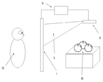
- FIG. 2 is a diagram illustrating a configuration example of the display device of the present invention.
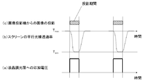
- FIG. 3 shows an example of the timing at which the image projector projects an image on the screen (the projection of the image starts from the moment when the screen starts switching from the light transmission state to the light scattering state, and the screen completely moves from the light scattering state.
- FIG. 6 is a diagram showing (at the moment when the switching to the light transmission state is completed, the projection of the image is finished).
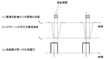
- FIG. 4 is a diagram illustrating an example of the timing at which the image projector projects an image on the screen (the period during which a voltage is applied to the liquid crystal light control layer coincides with the period during which an image is projected from the image projector).
- FIG. 5 is a diagram illustrating an example of the timing at which the image projector projects an image on the screen (projecting an image from the image projector during a period in which the parallel light transmittance of the screen is the minimum T min ).
- FIG. 6 is a diagram illustrating an example of the relationship between the applied waveform and the response waveform of the screen according to the present invention.
- FIG. 7 is a diagram illustrating an example of the configuration of the image display apparatus according to the present invention in the fourth embodiment.
- FIG. 8 is a radiance spectrum diagram of the screen portion of the image display device according to the fourth embodiment.
- the description of the constituent requirements described below is an example (representative example) of an embodiment of the present invention, and is not specified by these contents.
- the image display apparatus according to the present invention includes a screen and an image projector for projecting an image onto the screen, and at least one screen is disposed with respect to the image projector.
- the screen of the present invention can be switched between a light transmission state and a light scattering state.
- the image projector is one of the screens.
- An image is projected onto a part or the whole, and the screen and the image projector are synchronized so that the image projector does not project an image when the screen is in a light transmitting state.
- this synchronization switching at a speed that cannot be followed by the human eye, when the image is projected onto the screen, the image appears to be raised.
- light refers to visible light (wavelength 380 to 800 nm).
- the screen used in the present invention is a screen that can be switched to a light scattering state by applying a voltage in a light transmitting state when no voltage is applied.
- the screen of the present invention is transparent in normal use (no voltage applied) in applications such as windows and showcases, and can display an image in a light scattering state when a voltage is applied.
- the screen includes a transparent substrate, at least one of which is included in the screen, and a pair of substrates with electrodes disposed to face each other, and a dielectric anisotropy is positive between the pair of substrates with electrodes. It has a liquid crystal light control layer containing a composite containing a certain chiral nematic liquid crystal phase and a polymer resin phase.
- Switching between the light transmission state and the light scattering state can be realized by electrically driving the liquid crystal light control layer.
- the liquid crystal light control layer a composite of a transmission-scattering liquid crystal phase and a polymer resin phase that can be switched between a light transmission state and a light scattering state by electric drive can be used.
- the liquid crystal light control layer used in the present invention is in a light transmissive state when no voltage is applied, and is switched to a light scattering state by a DC voltage, an AC voltage, a pulse voltage, or a combination thereof having an effective value equal to or greater than a threshold value.
- the liquid crystal light control layer may be a reverse mode drive that returns to a light transmissive state when the applied voltage is removed, or a memory mode drive that applies a voltage only when switching between the light transmissive state and the light scattering state.
- a thing may be used.
- the screen of the present invention has a high contrast between the light transmission state and the light scattering state, so that a clear image can be displayed without particularly increasing the light source of the image projector.
- the screen is driven such that the light transmitting state and the light scattering state are periodically switched, and the frequency is 40 Hz or more and 100 Hz or less.
- the light scattering state in the present invention refers to a state where the parallel light transmittance is less than 30%, and the light transmissive state in the present invention refers to a state where the parallel light transmittance is 80% or more.
- a state in which the screen is driven by periodically switching between a light transmission state and a light scattering state may be expressed as a display mode.
- the normal cycle drive means that the drive is performed exactly the same every cycle. However, a different drive may be included as long as it does not depart from the spirit of the present invention.
- the periodic switching between the light transmission state and the light scattering state of the screen used in the present invention has a frequency of 40 Hz or more, preferably 45 Hz or more, 100 Hz or less, preferably 70 Hz or less, more preferably 60 Hz or less. When the frequency is lower than 40 Hz, flickering occurs on the screen in the display mode.
- the duty ratio of the periodic switching of the screen used in the present invention is 0.01 or more and 0.20 or less.
- the duty ratio of the screen is a ratio of time in the light scattering state in the periodic switching between the light transmitting state and the light scattering state.
- the duty ratio of the periodic switching of the screen of the present invention is 0.01 or more, preferably 0.05 or more, while the upper limit is 0.20 or less, preferably 0.15 or less.
- the smaller the duty ratio the smaller the haze of the screen in the display mode, and the background transparency is improved.
- the duty ratio is 0.20 or less, when an image is displayed in the display mode, the background can be seen well even in a dark place such as a room.
- the larger the duty ratio the clearer the displayed image.
- both video visibility and background transparency can be achieved.
- the parallel light transmittance and tau ON of less than 30% of the time ⁇ ON / ( ⁇ ON + ⁇ OFF)
- ⁇ ON / ( ⁇ ON + ⁇ OFF) is preferably 0.01 or more, and more preferably 0.05 or more.
- it is preferably 0.20 or less, and more preferably 0.15 or less.
- the instantaneous parallel light transmittance can be measured by using a commercially available high-speed compatible spectrometer, high-speed compatible luminance meter, or the like.
- the duty ratio of the pulse voltage having an effective value exceeding the threshold of the liquid crystal light control layer is 0.01 to 0.20 in the liquid crystal light control layer having a frequency of 40 Hz to 100 Hz. This can be realized by applying a burst voltage (hereinafter, it may be expressed as a pulse voltage or a burst voltage).
- the parallel light transmittance when a voltage is applied to the liquid crystal light control layer of the screen, it takes a finite time for the parallel light transmittance to be reduced when switching to the light scattering state, while on the other hand, It also takes a finite time for the parallel light transmittance to increase. Due to the presence of these transient states in which the parallel light transmittance fluctuates with time, the parallel light transmittance at the timing when the parallel light transmittance is low or the light scattering state is originally desired at the timing when the light is desired to be in the light scattering state. Inconvenience that the display mode is high, and as a result, the transparency of the display mode is reduced and the visibility of the display image is lowered.
- both the rising response time ⁇ 1 and the falling response time ⁇ 2 are 3.0 ms or less. More preferably, both are 2.0 ms or less.
- the parallel light transmittance of the screen is preferably less than 30% and more preferably less than 20% during the period in which the image projector projects an image. It is. In other periods, the higher the parallel light transmittance of the screen is, the better, and preferably 80% or more. On the other hand, in the transient state where the parallel light transmittance of the screen is 30% or more and less than 80%, sufficient visibility is not obtained even when the image is projected, but the transparency is low. is there.
- this transient state can be shortened, so that both the visibility of the image and the transparency of the background can be achieved. Further, it is preferable that the values of ⁇ 1 and ⁇ 2 are the same or approximate values because synchronization control is facilitated.
- the haze of the light scattering state portion of the screen of the present invention is defined by the measuring method of JIS K7136 (2000).
- haze means what was measured as a time average.
- the radiance of the display image in the image display device of the present invention is calculated by integrating the spectral radiance measured in JIS Z8724 (1997) in the visible light wavelength region.
- the duty ratio of periodic switching By adjusting the duty ratio of periodic switching, it is possible to select whether to emphasize the background or the video. That is, by reducing the duty ratio of periodic switching, the haze of the screen in the display mode can be reduced, but the radiance of the display image is also reduced. Conversely, increasing the duty ratio of the periodic switching increases the haze of the screen in the display mode, but increases the radiance of the display image.
- the haze in the display mode when applying a burst voltage having a frequency of 40 Hz to 100 Hz and a duty ratio of 0.01 to 0.20 is preferably 20% or less, and 15% or less. Is more preferable. Moreover, 1% or more is preferable and 5% or more is still more preferable. If the haze is not too large, the background transparency tends to be good, and if it is not too small, the brightness of the display image tends to be ensured to be visible.
- the positional relationship between the screen and the image projector in the present invention may be a rear projection system in which the viewer and the image projector face each other with the screen interposed therebetween, or a front projection system in which the viewer and the image projector are on the same side with respect to the screen.
- the former may be used when back scattering is strong, and the latter may be used when forward scattering is strong.
- You may install so that the light emission port of an image projector may become perpendicular
- the contrast of the display image is calculated by (white display radiance) / (black display radiance).
- the luminance ratio is preferably a specific value in the incident direction of the specific range of the image.
- the image projector projects an image on a part or the whole of the screen, and when the screen is in a light transmission state, the image projector Synchronize so that the image is not projected.
- the screen is driven so that the light transmission state and the light scattering state of the screen are periodically switched.
- the ratio of the radiance of white display to black display is 30 or more when the incident direction of the image projected from the image projector is within 30 ° with respect to the screen. Furthermore, it is preferable that it is 60 or more.
- the liquid crystal light control layer of the screen used in the present invention scatters light by a composite structure of a focal conic phase of chiral nematic liquid crystal and a network polymer.
- the focal conic phase which is a random liquid crystal polydomain structure, and a random network polymer structure, incident light is scattered over a wide range and a wide viewing angle is given. Even when viewed, the visibility of the image is improved.
- the screen of the present invention is in a light transmission state when no voltage is applied, and the haze at this time is preferably 10% or less. Further, it is preferably 8% or less, particularly preferably 5% or less. Moreover, it becomes a light-scattering state at the time of voltage application, and it is preferable that haze switches to 85% or more by applying the continuous wave of a DC voltage or an AC voltage to a screen, and it is preferable to become 90% or more.
- the upper limit is 100%, and the higher the better. Within these ranges, the visibility of the displayed image tends to be good.
- the upper limit of the operating temperature of the screen of the present invention is the liquid crystal-isotropic phase transition temperature (Tni) of the chiral nematic liquid crystal phase, but the response time tends to be longer at low temperatures. Therefore, the operating temperature range is preferably ⁇ 10 ° C. or higher, more preferably 0 ° C. or higher. Moreover, it is preferably 60 ° C. or lower, and more preferably 40 ° C. or lower.
- the screen of the present invention has a chiral substrate having at least one transparent substrate and a pair of substrates with electrodes disposed opposite to each other, and positive dielectric anisotropy between the pair of substrates with electrodes.
- a liquid crystal light control layer including a composite including a nematic liquid crystal phase and a polymer resin phase is included.
- the liquid crystal light control layer used for the screen of the present invention includes a composite containing a chiral nematic liquid crystal phase having a positive dielectric anisotropy and a polymer resin phase. This scheme is known as PSCT.
- PSCT the drive mode of the reverse mode PSCT will be described.
- reverse mode PSCT when no voltage is applied, almost all of the liquid crystal helical axes are in a planar phase facing the direction perpendicular to the substrate and take a light transmission state.
- the liquid crystal helical axis undergoes a phase transition to a focal conic phase in a random direction, resulting in a light scattering state.
- the parallel light transmittance of the screen can be controlled.
- the liquid crystal molecule major axis undergoes phase transition to a homeotropic phase in a direction perpendicular to the substrate, resulting in a light transmission state.
- the chiral nematic liquid crystal used in the screen of the present invention has a positive dielectric anisotropy. Since the dielectric anisotropy of the chiral nematic liquid crystal of the present invention is positive, both a decrease in T min and a decrease in ⁇ 1 and ⁇ 2 can be achieved.
- the dielectric anisotropy value ( ⁇ ) of the chiral nematic liquid crystal is not particularly limited as long as it is positive, but is preferably 5 or more, and more preferably 8 or more for reducing the driving voltage of the screen.
- numerator which comprises a chiral nematic liquid crystal does not have absorption of the wavelength which overlaps with the absorption wavelength of an initiator.
- the liquid crystal itself may be an assembly of liquid crystalline compounds exhibiting a cholesteric phase, or a chiral nematic liquid crystal may be formed by adding a chiral agent to the nematic liquid crystal. From the viewpoint of designing the liquid crystal composition, it is preferable to add a chiral agent to the nematic liquid crystal according to the purpose and control the chiral pitch length (p) and the liquid crystal-isotropic phase transition temperature (Tni).
- d / p is 1 or more, where d is the distance between the substrates with electrodes and p is the chiral pitch length of the chiral nematic liquid crystal.
- d / p is more preferably 2 or more, and still more preferably 4 or more. Further, d / p is preferably 20 or less, and particularly preferably 12 or less.
- the threshold voltage from the focal conic phase to the homeotropic phase is increased, and even when a high voltage is applied, the light transmission state is not changed and the light scattering state can be maintained. Therefore, the rising response time ⁇ 1 can be shortened.
- the screen drive voltage threshold voltage from the planar phase to the focal conic phase
- the chiral pitch length p of the chiral nematic liquid crystal is preferably 0.3 ⁇ m or more, and more preferably 0.8 ⁇ m or more.
- the chiral pitch length p is preferably 3 ⁇ m or less, more preferably 2 ⁇ m or less. If the chiral pitch length p is not too small, the screen drive voltage tends to be kept low, and if it is not too large, the contrast tends to be high. Since p is generally inversely proportional to the concentration of the chiral agent, the concentration of the chiral agent may be determined by calculating backward from the value of the required chiral pitch length p.
- the screen finally obtained is colored when no voltage is applied, and is out of the visible light range. In some cases, it becomes colorless and transparent when no voltage is applied, so the chiral pitch length p may be selected according to the purpose.
- the distance d between the substrates with electrodes of the screen of the present invention needs to be not less than the chiral pitch length p of the chiral nematic liquid crystal to be used, and is usually preferably 3 ⁇ m or more, more preferably 5 ⁇ m or more.
- the distance d is preferably 100 ⁇ m or less, and more preferably 20 ⁇ m or less.
- the light transmittance of the screen when no voltage is applied decreases as the distance d increases, and the response time of the display may become longer.
- d is too small, the light-shielding characteristic during driving is reduced, and in the case of a large area screen, the screen may be short-circuited. By being in the above range, these requirements can be satisfied in a balanced manner.
- Tni of the chiral nematic liquid crystal is preferably 50 ° C. or higher, and more preferably 70 ° C. or higher, because the upper temperature limit at which the screen can operate is determined by Tni of the chiral nematic liquid crystal.
- Tni increases, the viscosity tends to increase, so that it is preferably 200 ° C. or lower, and more preferably 150 ° C. or lower.
- the nematic liquid crystal may be any known one, and the molecular skeleton, substituent, and molecular weight of the constituent molecules are not particularly limited, and may be a synthetic product or a commercial product.
- the dielectric anisotropy of the nematic liquid crystal is preferably positive and large in order to make the dielectric anisotropy of the chiral nematic liquid crystal phase of the screen and the chiral nematic liquid crystal of the liquid crystal composition positive.
- a polymerization initiator it is preferable from the viewpoint of shortening the curing time of the polymerizable monomer that each molecule constituting the constituent molecule does not have absorption at a wavelength overlapping the absorption wavelength of the initiator.
- the chiral agent may be any chiral compound that is compatible with the host liquid crystal, may be a synthetic product or a commercial product, may exhibit liquid crystal properties, or may have a polymerizable functional group. Good. Further, dextrorotatory or levorotatory may be used, and a dextrorotatory chiral agent and a levorotatory chiral agent may be used in combination.
- the chiral agent those having a large dielectric anisotropy per se and a low viscosity are preferable from the viewpoints of reduction in driving voltage and response speed of the screen, and the helical agent is an index of the force for twisting the liquid crystal. A larger Twisting Power is preferable.
- the polymerization initiator does not have absorption at a wavelength that overlaps the absorption wavelength of the initiator.
- Examples of the chiral agent include CB15 (trade name, manufactured by Merck), C15 (trade name, manufactured by Merck), S-811 (trade name, manufactured by Merck), R-811 (trade name, manufactured by Merck), S-1011 (trade name, manufactured by Merck), R-1011 (trade name, manufactured by Merck) and the like.
- the polymer resin phase of the present invention is preferably formed by curing a specific polymer precursor.
- the polymer resin phase of the present invention is preferably 10% by mass or less, and more preferably 7% by mass or less, with respect to the chiral nematic liquid crystal phase. Moreover, it is preferable that it is 0.1 mass% or more, and it is preferable that it is 1 mass% or more.
- the ratio of the polymer resin phase is not too small, the polymer resin phase becomes mechanically tough and tends to be excellent in repeated durability.
- the liquid crystal molecules can receive sufficient interface interaction, the contrast and response speed of the screen may be increased.
- the ratio of the polymer resin phase is not too large, an increase in driving voltage is suppressed and the transparency of the screen tends to be high.
- the polymer resin used in the polymer resin phase of the present invention is not particularly limited as long as the effects of the present invention are not impaired, but is obtained by curing a mixture containing a polymer precursor represented by the following general formula (1). Is preferably used because it tends to achieve both a reduction in the minimum parallel light transmittance T min when a screen voltage is applied and a shortening of ⁇ 1 and ⁇ 2 .
- a 1 and A 2 each independently represent a hydrogen atom or a methyl group
- Ar 1 , Ar 2 and Ar 3 each independently represent a divalent aromatic hydrocarbon ring group which may have a substituent or a divalent aromatic heterocyclic group which may have a substituent.
- X 1 and X 2 are each independently a direct bond, a carbon double bond, a carbon triple bond, an ether bond, an ester bond, a linear alkylene group having 1 to 6 carbon atoms which may have a substituent, or a substituent.
- R 1 and R 2 are each independently a linear alkylene group having 1 to 6 carbon atoms which may have a substituent, or a linear chain having 1 to 6 carbon atoms which may have a substituent.
- at least one of Ar 1 , Ar 2 and Ar 3 is a divalent aromatic condensed ring group which may have a substituent or a divalent aromatic which may have a substituent.
- the divalent aromatic hydrocarbon ring group which may have a substituent for Ar 1 , Ar 2 and Ar 3 is not particularly limited as long as it does not impair the effects of the present invention.
- the hydrocarbon ring group is a divalent group obtained by removing two hydrogen atoms from a single ring or a condensed ring formed by condensation of 2 to 4 thereof. Specific examples include a benzene ring and a naphthalene ring.
- the number of carbon atoms is preferably 6 or more, and on the other hand, it is preferably 30 or less, more preferably 26 or less, and particularly preferably 18 or less from the viewpoint of curability during polymerization. Specific examples include the following structures.
- the divalent aromatic hydrocarbon ring group which may have a substituent of Ar 1 , Ar 2 and Ar 3 has the following structure in particular, and the curability of the polymer precursor is high. preferable.
- Examples of the substituent that the divalent aromatic hydrocarbon ring group of Ar 1 , Ar 2 and Ar 3 may have include a fluorine atom, a chlorine atom, a hydroxyl group, a cyano group, a methyl group, an ethyl group, n- Propyl group, isopropyl group, methoxy group, ethoxy group, n-propoxy group, isopropoxy group, n-butyl group, isobutyl group, t-butyl group and the like can be mentioned.
- the divalent aromatic heterocyclic group which may have a substituent for Ar 1 , Ar 2 and Ar 3 is not particularly limited as long as it does not impair the effects of the present invention.
- the number of carbon atoms is preferably 6 or more, and on the other hand, it is preferably 30 or less, more preferably 26 or less, and particularly preferably 18 or less from the viewpoint of curability during polymerization.
- Specific examples include the following structures.
- the divalent aromatic heterocyclic group which may have a substituent of Ar 1 , Ar 2 and Ar 3 , the following structure is particularly preferable among the above, since the curability of the polymer precursor is high. .
- Examples of the substituent that the divalent aromatic heterocyclic group represented by Ar 1 , Ar 2 and Ar 3 may have include a fluorine atom, a chlorine atom, a hydroxyl group, a cyano group, a methyl group, an ethyl group, and n-propyl.
- X 1 and X 2 are each independently a direct bond, a carbon double bond, a carbon triple bond, an ether bond, an ester bond, a linear alkylene group having 1 to 6 carbon atoms which may have a substituent, or a substituent.
- a straight-chain oxyalkylene group having 1 to 6 carbon atoms which may have a group, preferably a direct bond, an ether bond, an ester bond or a methylene group.
- the substituents that may be included are fluorine atom, chlorine atom, hydroxyl group, cyano group, methyl group, ethyl group, n-propyl group, isopropyl group, methoxy group, ethoxy group, n-propoxy group, isopropoxy group Group, n-butyl group, isobutyl group, t-butyl group and the like, preferably fluorine atom, hydroxyl group, cyano group, methyl group and methoxy group.
- R 1 and R 2 are each independently a linear alkylene group having 1 to 6 carbon atoms which may have a substituent, or a linear chain having 1 to 6 carbon atoms which may have a substituent.
- An oxyalkylene group or a linear alkyl ester group having 2 to 6 carbon atoms is represented.
- the straight chain alkyl ester group having 2 to 6 carbon atoms represents, for example, the following structure.
- R 1 and R 2 may have include a fluorine atom, chlorine atom, hydroxyl group, cyano group, methyl group, ethyl group, n-propyl group, isopropyl group, methoxy group, ethoxy group, n -Propoxy group, isopropoxy group, n-butyl group, isobutyl group, t-butyl group and the like are mentioned, and preferred are fluorine atom, hydroxyl group, cyano group, methyl group and methoxy group.
- At least one of Ar 1 , Ar 2 and Ar 3 is a divalent aromatic condensed ring group which may have a substituent or a divalent aromatic heterocyclic ring which may have a substituent. It is a group.
- a divalent aromatic condensed ring group which may have a substituent or a divalent aromatic heterocyclic group which may have a substituent in the molecule the rigidity of the polymer resin phase after curing Tends to shorten ⁇ 1 and ⁇ 2, which is preferable.
- the polymer precursor represented by the general formula (1) is a polymer precursor represented by the following general formula (2).
- a 1 and A 2 each independently represent a hydrogen atom or a methyl group
- Ar 4 represents a divalent aromatic hydrocarbon condensed ring group which may have a substituent or a divalent hetero condensed ring group which may have a substituent
- R 1 and R 2 each independently represents an alkylene group having 2 to 6 carbon atoms which may have a substituent
- p and q each independently represents 0 or 1.
- Specific examples of the divalent aromatic hydrocarbon ring group that may have a substituent of Ar 4 and the divalent heterocyclic group that may have a substituent include those listed for Ar 1. It is synonymous and the substituent which you may have is also synonymous. Among these, the structure represented below is preferable because the curability of the polymer precursor is increased.
- Ar 4 is preferably a divalent aromatic hydrocarbon condensed ring group which may have a substituent because the mechanical strength of the polymer resin phase is increased, and among them, the number of carbon atoms is 6
- the molecular size is too large, the degree of spatial freedom for the polymer precursor to undergo a polymerization reaction is reduced, and the polymerization reaction does not occur sufficiently. In particular, it is preferably 18 or less.
- Ar 4 is preferably a divalent benzene ring which may have a substituent or a divalent naphthalene ring which may have a substituent among the above, and has a substituent. A good divalent naphthalene ring is particularly preferable because of high curability of the polymer precursor.
- Ar 4 has a strong electron donating property to the polymerizable group.
- the position at which Ar 4 is bonded to —O— is not particularly limited, but the molecule preferably has a linear structure.
- the benzene ring is bonded to the 1,4-position, and the naphthalene ring monocycle is bonded to the 1,4-position or the 2,6-position.
- the polymer precursor used in the liquid crystal light control layer of the present invention only one kind of polymer precursor represented by the above formula (1) may be used, or two or more kinds may be used in combination.
- the ratio of the polymer precursor represented by the general formula (1) used for the screen of the present invention and the other polymer precursor is not particularly limited as long as the effects of the present invention are not impaired, but the general formula (1) ) Is preferably 30% by mass or more, more preferably 50% by mass or more, and most preferably 80% by mass or more.
- the proportion of the polymer precursor represented by the above formula (1) is too small, one of screen production in a short time, high contrast, short response time, or a plurality of the precursors may not be sufficient.
- the upper limit of the polymer precursor represented by the above formula (1) is 100% by mass.
- the chiral nematic liquid crystal phase of the screen of the present invention has a polymerization initiator, a light stabilizer, an antioxidant, a thickener, a polymerization inhibitor, a photosensitizer, an adhesive, an antifoaming agent, a surfactant and the like. You may do it.
- content of the said other component can be mix
- the curing method of the polymer precursor may be either photocuring or heat curing, but photocuring is preferable, and among the photocuring, curing with ultraviolet rays or near ultraviolet rays is particularly preferable.
- the light source for photopolymerization may be any light source having a spectrum at the absorption wavelength of the radical photopolymerization initiator used, and typically any light source capable of irradiating light with a wavelength of 220 nm to 450 nm. . Examples include high pressure mercury lamps, ultra high pressure mercury lamps, halogen lamps, metal halide lamps, UV-LEDs (Light Emitting Diodes), blue LEDs, white LEDs, and the like.
- a heat ray cut filter an ultraviolet ray cut filter, a visible light cut filter, or the like may be used in combination.
- Light may be applied to at least one surface from the transparent substrate of the screen, and if both surfaces of the substrate sandwiching the liquid crystal composition are transparent, both surfaces may be irradiated with light. Light irradiation may be performed at one time or may be performed by dividing into several times. So-called PSCOF (Phase Separated Composite Organic Film) (V. Vorflusev and S. Kumar, Science 283, which distributes the irradiance of light in the thickness direction of the screen and continuously changes the density of the polymer resin phase. 1903 (1999)).
- PSCOF Phase Separated Composite Organic Film
- the irradiance of the light irradiated on the screen typically 0.01 mW / cm 2 or more, preferably 1 mW / cm 2 or more, more preferably 10 mW / cm 2 or more, particularly preferably 30 mW / cm 2 That's it. If the irradiance is too small, the polymerization does not proceed sufficiently. Further, for photocuring of the liquid crystal composition, an integrated irradiation amount of usually 2 J / cm 2 or more, preferably 3 J / cm 2 or more may be given, and the light irradiation time may be determined according to the radiation intensity of the light source.
- the light irradiation is usually completed within 200 seconds, preferably within 60 seconds, while it is preferable to perform light irradiation for 10 seconds or more. If the light irradiation time is too short, the repetition durability of the screen may be inferior.
- the chiral nematic liquid crystal is dispersed or formed into a continuous layer in a thin transparent polymer, but the continuous layer exhibits the best contrast. Is formed.
- the screen used in the present invention is a transparent substrate at least one of which includes a pair of substrates with electrodes arranged opposite to each other, and a liquid crystal light control layer including a composite of a chiral nematic liquid crystal and a polymer resin between the substrates,
- the liquid crystal light control layer is obtained by curing a liquid crystal composition composed of a polymerizable monomer and a chiral nematic liquid crystal.
- the screen used in the present invention is not particularly limited as long as it is the above-mentioned screen, but a typical structure will be described below.
- At least one of the substrates is transparent, and preferably both are transparent.
- the material of the substrate include colorless transparent or colored transparent or opaque materials such as inorganic transparent materials such as glass and quartz, metals, metal oxides, semiconductors, ceramics, plastic plates, and plastic films.
- a thin film of metal oxide, metal, semiconductor, organic conductive material or the like is formed on the entire surface of the substrate or partially by a known coating method, printing method, vapor deposition method such as sputtering, or the like. is there. Alternatively, it may be partially etched after forming a conductive thin film.
- an ITO (mixture of indium oxide and tin oxide) electrode is deposited on a transparent polymer film such as PET or PEN, or a deposition method or printing method such as sputtering. It is desirable to use an electrode substrate formed by using, for example. A wiring for connecting the electrodes or connecting the electrodes and the outside may be provided on the substrate. For example, a segment driving electrode substrate, a matrix driving electrode substrate, an active matrix driving electrode substrate, or the like may be used.
- a strip-shaped electrode can be formed on one substrate in the direction of the short side of the strip, and a solid electrode can be used on the other to form a strip-shaped segment.
- a strip-shaped electrode can be used to form a matrix-like segment so that the strips face each other so as to be orthogonal.
- the electrode surface provided on the substrate is a protective film made of an organic compound such as polyimide, polyamide, polyvinyl alcohol, silicon, and cyanide, an inorganic compound such as SiO 2 , TiO 2 , and ZrO 2 , or a mixture thereof.
- the entire surface or a part thereof may be covered with an alignment film.
- the substrate may be aligned so that the liquid crystal is aligned with respect to the surface of the substrate. When the alignment is processed, any alignment processing can be used as long as the chiral nematic liquid crystal in contact has a planar structure. It doesn't matter.
- the two substrates may be homogeneously aligned, or may be a so-called hybrid in which one is homogeneously aligned and the other is homeotropic aligned.
- the electrode surface may be directly rubbed, or a normal alignment film such as polyimide used for TN (Twisted Nematic) liquid crystal, STN (Supper Twisted Nematic) liquid crystal, or the like may be used.
- a so-called photo-alignment method may be used in which the organic thin film on the substrate is irradiated with light having anisotropy such as linearly polarized light to give the film anisotropy.
- the polymer resin phase contained in the liquid crystal light control layer may have an alignment film function.
- the opposing substrate may have an adhesive layer including a resin body for adhering and supporting the substrate as appropriate at the periphery.
- the end face of the screen or the liquid crystal injection port used in the present invention is a tape such as an adhesive tape, a thermocompression bonding tape, a thermosetting tape, and / or a thermosetting resin, a photocurable resin, a moisture curable resin.
- Curable resins such as room temperature curable adhesives, anaerobic adhesives, epoxy adhesives, silicone adhesives, fluororesin adhesives, polyester adhesives, vinyl chloride adhesives, and thermoplastic resins
- This sealing may also work to prevent deterioration of the screen at the same time.
- the end face may be protected by covering the entire end face, or by pouring curable resins or thermoplastic resins into the screen from the end face and solidifying it. It may be covered with a kind.
- Spacers such as spherical or cylindrical glass, plastic, ceramic, or plastic film may be present between the substrates arranged to face each other.
- the spacer may be dispersed in the liquid crystal composition, or may be fixed in the liquid crystal light control layer between the substrates.
- the spacer may be dispersed on the substrate during screen assembly or mixed with an adhesive to bond the adhesive layer.
- the liquid crystal light control layer included in the screen used in the present invention is, for example, a sealing cell by forming an adhesive layer with a photo-curing adhesive or the like on a peripheral portion of a pair of electrodes facing each other via a spacer, Inject or inject liquid crystal composition in normal pressure or vacuum in the notch of one or more adhesive layers provided in advance, or apply the liquid crystal composition on one substrate using a coater, and After being sandwiched by a known method such as stacking the other substrate, it is formed by polymerization and curing by radiation such as ultraviolet light, visible light, or electron beam.
- a substrate with electrodes supplied continuously can be sandwiched between two rolls and the like, and a liquid crystal composition containing and dispersed a spacer can be fed between them, and then it can be photocured continuously. So productivity is high.
- At least one surface or both surfaces of the screen may be covered with an antireflection film, an antiglare film, an ultraviolet blocking film, or an antifouling film. For example, by covering the front and back of the screen with an antireflection film, reflection of external light on the substrate surface is prevented, and the appearance of the screen is improved.
- the image projector used in the present invention may be any one that can project an image in a time division manner, and includes, for example, a configuration in which a shutter is provided between a light source and a screen.
- a shutter a liquid crystal light valve or the like can be used in addition to a general mechanical shutter.
- a ferroelectric liquid crystal or a liquid crystal light valve using a transmission / scattering type liquid crystal mode may be used.
- a polarizing plate it is preferable that the polarization of the light emitted from the image projection device of the projector is aligned with the transmission axis of the light incident side polarizing plate of the shutter because the light use efficiency is increased.
- the projection timing of the image from the image projection apparatus may be directly synchronized with the driving timing at which the liquid crystal layer of the screen takes the light transmission state and the light scattering state.
- the light source may be turned on / off instead of the shutter.
- an LED capable of high-speed switching may be used as the light source.
- the image projector a commercially available liquid crystal projector, CRT (Cathode Ray Tube) projector, LED projector, laser projector, or the like can be used.
- a light source such as a lamp, LED, OLED, or laser may be used to modulate light with a light valve, a color filter, a mirror, or the like.
- a control device that controls the timing of projecting an image, it is preferable to use the control device in combination.
- At least one screen is disposed with respect to the image projector, and when the screen is in the light scattering state or while the light transmission state is changed to the light scattering state, the image projector is An image is projected onto a part or the whole of the screen, and is synchronized so that the image projector does not project an image when the screen is in a light transmitting state.
- FIG. 2 shows a configuration example of the display device of the present invention.
- Reference numeral 1 denotes a display screen, which is a rear projection system in which the image projector 2 and the observer O face each other.
- the observer O can see the background B (product) through the display screen 1.
- the display screen 1 and the image projector 2 are controlled in drive timing by a signal transmitted from the control device 3.
- the image display device of the present invention includes a control device.
- the control device performs control to periodically switch between the light transmission state and the light scattering state of the screen.
- FIGS. 3, 4, and 5 respectively show (a) voltage applied to the liquid crystal light control layer of the screen, (b) parallel light transmittance of the screen, and (c) image projection of the image projector.
- a time chart is shown.
- FIG. 3 shows an example in which the projection of an image starts from the moment when the screen starts to switch from the light transmission state to the light scattering state, and the projection of the image ends at the moment when the screen ends from the light scattering state to the completely light transmission state. Show. In this case, the period during which the parallel light transmittance of the screen is smaller than T min, the image projector is that it is projecting an image.
- T min the period during which the parallel light transmittance of the screen is smaller than T min
- FIG. 4 shows a case where the period during which the voltage is applied to the liquid crystal light control layer and the period during which the image is projected from the image projector are matched.
- FIG. 5 shows a case where an image is projected from the image projector during a period in which the parallel light transmittance of the screen is the minimum T min .
- T min is preferably 30% or less.
- One image projector may be arranged on one screen, or two or more image projectors may be arranged on one screen. When two or more image projectors are arranged on one screen, the image may be projected on the same place on the screen, or the image may be projected on different places.
- Two or more screens may be arranged for one image projector. When two or more screens are arranged for one image projector, they can be arranged in a plane or in the depth direction.
- the image may be projected on only one segment, the image may be projected on two or more, or all segments .
- all the display areas may be synchronously driven at the same timing, or synchronously driven at different timings for each screen or segment. Also good. In the latter case, the visibility of the image can be improved by sequentially switching the image projection for each screen or segment and setting so that the image is always projected in any one of the display areas. For example, when the screen is divided into N segments, assuming that the frequency for periodically driving the screen is F (Hz), the duty ratio of the light scattering state per segment is set to 1 / N, and 1 is set for adjacent segments.
- the screen segments are arranged in strips, the segments are arranged in the short side direction, the scan lines are aligned with the long side directions, and the sub-scan lines are It can be matched with the long side direction of the segment.
- a light beam scanning method any of a raster scan method, a vector scan method, and an interlace method may be used.
- an image projector that draws an image by scanning a light beam an image projector using a laser as a light source is preferable in terms of high color reproducibility of an image and a small image projector.
- the response time of the screen was measured at room temperature of 25 ° C.
- a halogen lamp was used as the light source, and light was incident on the screen vertically while applying a predetermined burst voltage.
- the brightness L of the element transmitted light was measured using a multimedia display tester 3298F (manufactured by YOKOGAWA) as a detector.
- a digital oscilloscope was used to monitor the applied waveform and response waveform.
- the parallel light transmittance T (%) of the element was calculated by L / L 0 ⁇ 100 based on the brightness L 0 of the blank.
- T max the minimum value of the parallel light transmittance when voltage is applied
- T min the pulse voltage application start time
- t 2 the application end time
- ⁇ 1 the time until the parallel light transmittance reaches T 10 for the first time from t 1
- ⁇ 2 the parallel light transmission for the first time from t 2.
- the rate is the time to reach the T 90.
- T 10 0.1 ⁇ (T max ⁇ T min )
- T 90 0.9 ⁇ (T max ⁇ T min )
- the relationship between the applied waveform and the response waveform of the screen is shown in FIG.
- Applied waveform using a burst waveform as in FIG. 6, was applied by setting the frequency F and duty ratio D V to a predetermined value.
- the pulse amplitude V was 100 Vp-p.
- ⁇ ON the time when the parallel light transmittance of the screen is 30% or less
- ⁇ OFF the time when the screen is less than 30%
- ⁇ ⁇ 1 ⁇ 2 .
- ⁇ 1 is the dielectric constant in the major axis direction of the liquid crystal molecules
- ⁇ 2 is the dielectric constant in the uniaxial direction of the liquid crystal molecules.
- D represents the thickness of the liquid crystal layer.
- S represents the overlapping portion of the electrodes of the two electrode substrates. It represents the area of).
- Chiral nematic liquid crystal (a) 95.0 wt%, monomer represented by the following structural formula (II) (Ac-N, trade name, manufactured by Kawasaki Kasei Co., Ltd.) 2.4 wt%, represented by the following structural formula (III) Monomer (Mc-N, trade name, manufactured by Kawasaki Kasei Co., Ltd.) 2.4 wt% and polymerization initiator represented by the following structural formula (IV) (Lucirin TPO, trade name, manufactured by BASF JAPAN) 0.2 wt% It mixed, stirred and filtered and the liquid-crystal composition (A) of Tni 94 degreeC was prepared.
- the cell was irradiated with UV light (wavelength 365 nm) on both sides at 1.6 J on one side at a room temperature at a room temperature to cure the monomer, and a screen (A-1) was obtained.
- the produced screen (A-1) had a transparent appearance, and showed reverse mode driving that changed to an opaque appearance when a voltage was applied.
- V (Vp-p) a rectangular wave of 100 Hz
- ultraviolet light wavelength 365 nm
- the produced screen (A-2) had a transparent appearance, and showed reverse mode driving that changed to an opaque appearance when a voltage was applied.
- V (Vp-p) a rectangular wave voltage
- the glass substrate used was a transparent electrode provided with an alignment film subjected to a homogeneous alignment treatment.
- the cell was irradiated with UV light (wavelength 365 nm) on both sides at a temperature of room temperature and 3.0 J on one side on both sides to cure the monomer to obtain a screen (B-1).
- the produced screen (B-1) had a transparent appearance, and showed a reverse mode drive that changed to an opaque appearance when a voltage was applied.
- V (Vp-p) a rectangular wave voltage
- a transparent electrode provided with an alignment film subjected to homeotropic alignment treatment was used.
- This cell was irradiated with ultraviolet light (wavelength 365 nm) on each side at a temperature of room temperature at a temperature of 3.0 J on both sides by 3.0 J to cure the monomer to obtain a screen (C-1).
- the produced screen (C-1) had a transparent appearance, and showed reverse mode driving that changed to an opaque appearance when a voltage was applied.
- V (Vp-p) a rectangular wave voltage
- Example 4 Using the screen (A-1) of Example 1, the image display device shown in FIG. 7 was produced.
- reference numeral 11 is a light source
- reference numeral 12 is a liquid crystal light valve
- reference numeral 13 is a lens
- reference numeral 14 is a light chopper
- reference numeral 15 is an image projector
- reference numeral 16 is a screen
- reference numeral 17 is an image display device
- reference numeral 18 is luminance. It is a total.
- Table 2 shows the screen optical characteristics (D, haze at OFF, ⁇ 1 , ⁇ 2 , T min ) and see-through display characteristics with respect to the voltage waveform parameters (V, D V , F) applied to the screen (A-1).
- Display haze radiance contrast, flicker
- “ ⁇ ” indicates that no flicker is seen, and “ ⁇ ” indicates that flicker is seen.
- the haze at the time of display was 10.2%, the background was not blurred, and was clearly visible.
- the radiance C / R was 127.9, and the image looked bright. Also, no flicker was seen on the screen.
- Example 5 and 6 Screen parameter of the voltage waveform (V, D V, F) a relative except for changing as described in Table 2, the parameters of the voltage waveform using the same image display apparatus as in Example 4 (V, D V, F )
- the optical characteristics (D, haze at OFF, ⁇ 1 , ⁇ 2 , T min ) and see-through display characteristics (haze at display, radiance contrast, flicker) were evaluated.
- D was in the range of 0.01 to 0.20.
- the haze at OFF was 10% or less.
- Both ⁇ 1 and ⁇ 2 were 3.0 msec or less.
- T min was 30% or less in all cases.
- the radiance C / R was 60 or more, and the image looked bright. Also, no flicker was seen on the screen.
- Example 7 to 11 Except that the screen is changed to the screen (A-2), it is driven using the same image display device as in Examples 4 to 6, and the optical characteristics of the screen with respect to the voltage waveform parameters (V, D V , F) ( D, haze at OFF, ⁇ 1 , ⁇ 2 , T min ) and see-through display characteristics (display haze, radiance contrast, flicker).
- Table 2 shows the parameters (V, D V , F) of the voltage waveform.
- D was in the range of 0.01 to 0.20.
- the haze at OFF was 10% or less.
- Both ⁇ 1 and ⁇ 2 were 3.0 msec or less.
- T min was 30% or less in all cases.
- the radiance C / R was 60 or more, and the image looked bright. Also, no flicker was seen on the screen.
- Example 12 to 14 Except that the screen is changed to the screen (B-1), driving is performed using the same image display apparatus as in Examples 4 to 6, and the optical characteristics of the screen with respect to the voltage waveform parameters (V, D V , F) ( D, haze at OFF, ⁇ 1 , ⁇ 2 , T min ) and see-through display characteristics (display haze, radiance contrast, flicker).
- the voltage waveform parameters (V, D V , F) are shown in Table 2.
- D was in the range of 0.01 to 0.20.
- the haze at OFF was 10% or less.
- Both ⁇ 1 and ⁇ 2 were 3.0 msec or less.
- T min was 30% or less in all cases.
- the radiance C / R was 60 or more, and the image looked bright. Also, no flicker was seen on the screen.
- ⁇ 2 was as slow as 10 msec or more.
- the haze at the time of display was 20% or more, the background was blurred, and it was not clearly visible.
- the radiance C / R was 60 or less, and the image did not appear bright. Also, the screen flickered.
- Display screen 2 Image projector 3 Control device 11
- Light source 12 Liquid crystal light valve 13
- Lens 14 Light chopper 15
- Image projector 16 Screen 17
- Image display device 18 Luminance meter O Observer B Background L Projection light
Landscapes
- Physics & Mathematics (AREA)
- Chemical & Material Sciences (AREA)
- Nonlinear Science (AREA)
- General Physics & Mathematics (AREA)
- Crystallography & Structural Chemistry (AREA)
- Optics & Photonics (AREA)
- Mathematical Physics (AREA)
- Engineering & Computer Science (AREA)
- Organic Chemistry (AREA)
- Materials Engineering (AREA)
- Dispersion Chemistry (AREA)
- Liquid Crystal (AREA)
- Transforming Electric Information Into Light Information (AREA)
- Overhead Projectors And Projection Screens (AREA)
Priority Applications (4)
| Application Number | Priority Date | Filing Date | Title |
|---|---|---|---|
| EP13842911.3A EP2902843B1 (fr) | 2012-09-27 | 2013-09-26 | Dispositif d'affichage d'image |
| JP2014538603A JP6210067B2 (ja) | 2012-09-27 | 2013-09-26 | 画像表示装置 |
| CN201380050868.6A CN104685415B (zh) | 2012-09-27 | 2013-09-26 | 图像显示装置 |
| US14/671,476 US20150205149A1 (en) | 2012-09-27 | 2015-03-27 | Image display device |
Applications Claiming Priority (2)
| Application Number | Priority Date | Filing Date | Title |
|---|---|---|---|
| JP2012-215006 | 2012-09-27 | ||
| JP2012215006 | 2012-09-27 |
Related Child Applications (1)
| Application Number | Title | Priority Date | Filing Date |
|---|---|---|---|
| US14/671,476 Continuation US20150205149A1 (en) | 2012-09-27 | 2015-03-27 | Image display device |
Publications (1)
| Publication Number | Publication Date |
|---|---|
| WO2014051002A1 true WO2014051002A1 (fr) | 2014-04-03 |
Family
ID=50388397
Family Applications (1)
| Application Number | Title | Priority Date | Filing Date |
|---|---|---|---|
| PCT/JP2013/076137 Ceased WO2014051002A1 (fr) | 2012-09-27 | 2013-09-26 | Dispositif d'affichage d'image |
Country Status (5)
| Country | Link |
|---|---|
| US (1) | US20150205149A1 (fr) |
| EP (1) | EP2902843B1 (fr) |
| JP (1) | JP6210067B2 (fr) |
| CN (1) | CN104685415B (fr) |
| WO (1) | WO2014051002A1 (fr) |
Cited By (8)
| Publication number | Priority date | Publication date | Assignee | Title |
|---|---|---|---|---|
| WO2015125207A1 (fr) * | 2014-02-18 | 2015-08-27 | パイオニア株式会社 | Dispositif de commande d'affichage |
| WO2015132907A1 (fr) * | 2014-03-05 | 2015-09-11 | パイオニア株式会社 | Dispositif de commande d'affichage |
| CN105607294A (zh) * | 2015-02-12 | 2016-05-25 | 明基材料有限公司 | 单向透视视窗系统 |
| JP2016109953A (ja) * | 2014-12-09 | 2016-06-20 | アキレス株式会社 | 反射型プロジェクタースクリーン |
| KR20180051577A (ko) * | 2015-09-08 | 2018-05-16 | 메르크 파텐트 게엠베하 | 광 변조 소자 |
| US10018849B2 (en) | 2015-01-20 | 2018-07-10 | Benq Materials Corporation | One-way vision window system |
| JP2021184062A (ja) * | 2020-05-22 | 2021-12-02 | 大日本印刷株式会社 | 調光装置 |
| JP7590746B1 (ja) | 2024-07-12 | 2024-11-27 | 株式会社正興電機製作所 | 調光装置 |
Families Citing this family (10)
| Publication number | Priority date | Publication date | Assignee | Title |
|---|---|---|---|---|
| TWI559071B (zh) * | 2015-06-26 | 2016-11-21 | 明基材料股份有限公司 | 投影系統 |
| CN104991413A (zh) * | 2015-07-22 | 2015-10-21 | 明基材料有限公司 | 投影系统 |
| CN106488208B (zh) * | 2017-01-03 | 2020-03-31 | 京东方科技集团股份有限公司 | 一种显示装置及显示方法 |
| CN107742492B (zh) * | 2017-11-01 | 2021-10-01 | 京东方科技集团股份有限公司 | 透明显示系统及其显示方法 |
| CN109001930B (zh) * | 2018-07-13 | 2021-11-02 | 华南师范大学 | 一种电响应红外反射器件及其制备方法 |
| JP6749007B2 (ja) * | 2018-08-07 | 2020-09-02 | パナック株式会社 | 宣伝広告表示方法 |
| CN109656043A (zh) * | 2019-02-01 | 2019-04-19 | 腾讯科技(深圳)有限公司 | 显示装置及图像显示方法 |
| CN112505995A (zh) * | 2020-12-15 | 2021-03-16 | 青岛海信激光显示股份有限公司 | 激光投影镜头及激光投影设备 |
| US20220413324A1 (en) * | 2021-06-29 | 2022-12-29 | Meta Platforms Technologies, Llc | Compact imaging optics using liquid crystal (lc) for dynamic glare reduction and sharpness enhancement |
| JP2023157168A (ja) * | 2022-04-14 | 2023-10-26 | シャープディスプレイテクノロジー株式会社 | 液晶表示装置 |
Citations (5)
| Publication number | Priority date | Publication date | Assignee | Title |
|---|---|---|---|---|
| JP2002541515A (ja) * | 1999-04-06 | 2002-12-03 | レヴェオ・インコーポレーテッド | 散乱及び透過動作モードを備えた電気光学グレージング構造体 |
| JP2004184979A (ja) | 2002-09-03 | 2004-07-02 | Optrex Corp | 画像表示装置 |
| JP2004184980A (ja) * | 2002-09-11 | 2004-07-02 | Asahi Glass Co Ltd | 複合表示装置 |
| JP2010531468A (ja) * | 2007-06-25 | 2010-09-24 | ヴライト イノヴェーションズ リミテッド | 高分子分散液晶構造 |
| WO2012060306A1 (fr) * | 2010-11-04 | 2012-05-10 | シャープ株式会社 | Système d'affichage, terminal mobile et équipement électronique |
Family Cites Families (10)
| Publication number | Priority date | Publication date | Assignee | Title |
|---|---|---|---|---|
| DE69229003T2 (de) * | 1992-05-18 | 1999-10-21 | Kent State University, Kent | Flüssigkristalline, lichtmodulierende vorrichtung und material |
| JP2991577B2 (ja) * | 1992-11-13 | 1999-12-20 | 日本放送協会 | 液晶素子の駆動方法、液晶装置および照明装置 |
| EP1546795A4 (fr) * | 2002-09-03 | 2006-11-15 | Optrex Kk | Systeme d'affichage d'images |
| WO2011043100A1 (fr) * | 2009-10-09 | 2011-04-14 | シャープ株式会社 | Écran, système d'affichage, terminal portable et dispositif électronique |
| TWI482839B (zh) * | 2010-01-26 | 2015-05-01 | Jnc Corp | 液晶組成物及液晶顯示元件 |
| US9792844B2 (en) * | 2010-11-23 | 2017-10-17 | Seminconductor Energy Laboratory Co., Ltd. | Driving method of image display device in which the increase in luminance and the decrease in luminance compensate for each other |
| US8953120B2 (en) * | 2011-01-07 | 2015-02-10 | Semiconductor Energy Laboratory Co., Ltd. | Display device |
| EP2692828B1 (fr) * | 2011-03-28 | 2019-12-04 | Mitsubishi Chemical Corporation | Élément à cristaux liquides et composition de cristaux liquides |
| EP2557140B1 (fr) * | 2011-08-09 | 2016-09-21 | Merck Patent GmbH | Milieu liquide cristallin |
| EP2703472B1 (fr) * | 2012-08-31 | 2018-07-04 | Merck Patent GmbH | Milieu liquide cristallin |
-
2013
- 2013-09-26 WO PCT/JP2013/076137 patent/WO2014051002A1/fr not_active Ceased
- 2013-09-26 JP JP2014538603A patent/JP6210067B2/ja active Active
- 2013-09-26 CN CN201380050868.6A patent/CN104685415B/zh active Active
- 2013-09-26 EP EP13842911.3A patent/EP2902843B1/fr active Active
-
2015
- 2015-03-27 US US14/671,476 patent/US20150205149A1/en not_active Abandoned
Patent Citations (5)
| Publication number | Priority date | Publication date | Assignee | Title |
|---|---|---|---|---|
| JP2002541515A (ja) * | 1999-04-06 | 2002-12-03 | レヴェオ・インコーポレーテッド | 散乱及び透過動作モードを備えた電気光学グレージング構造体 |
| JP2004184979A (ja) | 2002-09-03 | 2004-07-02 | Optrex Corp | 画像表示装置 |
| JP2004184980A (ja) * | 2002-09-11 | 2004-07-02 | Asahi Glass Co Ltd | 複合表示装置 |
| JP2010531468A (ja) * | 2007-06-25 | 2010-09-24 | ヴライト イノヴェーションズ リミテッド | 高分子分散液晶構造 |
| WO2012060306A1 (fr) * | 2010-11-04 | 2012-05-10 | シャープ株式会社 | Système d'affichage, terminal mobile et équipement électronique |
Non-Patent Citations (5)
| Title |
|---|
| "Ekisho Binran", 2000, MARUZEN CO., LTD., pages: 260 - 330 |
| "Ekisho Binran", 2000, MARUZEN CO., LTD., pages: 365 - 415 |
| "Liquid Crystal Device Handbook", vol. 142, 1989, NIHON KOGYO SHIMBUN, pages: 152 - 192 |
| See also references of EP2902843A4 |
| V. VORFLUSEV; S. KUMAR: "Phase Separated Composite Organic Film", SCIENCE, vol. 283, 1999, pages 1903 |
Cited By (14)
| Publication number | Priority date | Publication date | Assignee | Title |
|---|---|---|---|---|
| JPWO2015125207A1 (ja) * | 2014-02-18 | 2017-03-30 | パイオニア株式会社 | 表示制御装置 |
| WO2015125207A1 (fr) * | 2014-02-18 | 2015-08-27 | パイオニア株式会社 | Dispositif de commande d'affichage |
| WO2015132907A1 (fr) * | 2014-03-05 | 2015-09-11 | パイオニア株式会社 | Dispositif de commande d'affichage |
| JP2016109953A (ja) * | 2014-12-09 | 2016-06-20 | アキレス株式会社 | 反射型プロジェクタースクリーン |
| US10018849B2 (en) | 2015-01-20 | 2018-07-10 | Benq Materials Corporation | One-way vision window system |
| CN105607294A (zh) * | 2015-02-12 | 2016-05-25 | 明基材料有限公司 | 单向透视视窗系统 |
| KR20180051577A (ko) * | 2015-09-08 | 2018-05-16 | 메르크 파텐트 게엠베하 | 광 변조 소자 |
| JP2018538555A (ja) * | 2015-09-08 | 2018-12-27 | メルク パテント ゲゼルシャフト ミット ベシュレンクテル ハフツングMerck Patent Gesellschaft mit beschraenkter Haftung | 光変調素子 |
| JP7005486B2 (ja) | 2015-09-08 | 2022-01-21 | メルク パテント ゲゼルシャフト ミット ベシュレンクテル ハフツング | 光変調素子 |
| KR102656729B1 (ko) | 2015-09-08 | 2024-04-15 | 메르크 파텐트 게엠베하 | 광 변조 소자 |
| JP2021184062A (ja) * | 2020-05-22 | 2021-12-02 | 大日本印刷株式会社 | 調光装置 |
| JP7468142B2 (ja) | 2020-05-22 | 2024-04-16 | 大日本印刷株式会社 | 調光装置 |
| JP7590746B1 (ja) | 2024-07-12 | 2024-11-27 | 株式会社正興電機製作所 | 調光装置 |
| JP2026011631A (ja) * | 2024-07-12 | 2026-01-23 | 株式会社正興電機製作所 | 調光装置 |
Also Published As
| Publication number | Publication date |
|---|---|
| EP2902843A1 (fr) | 2015-08-05 |
| CN104685415B (zh) | 2016-08-24 |
| CN104685415A (zh) | 2015-06-03 |
| US20150205149A1 (en) | 2015-07-23 |
| JP6210067B2 (ja) | 2017-10-11 |
| EP2902843B1 (fr) | 2018-12-26 |
| JPWO2014051002A1 (ja) | 2016-08-22 |
| EP2902843A4 (fr) | 2015-11-18 |
Similar Documents
| Publication | Publication Date | Title |
|---|---|---|
| JP6210067B2 (ja) | 画像表示装置 | |
| JP6884849B2 (ja) | 画像表示装置 | |
| JP6724352B2 (ja) | 液晶素子、液晶組成物、液晶素子を用いたスクリーン及びディスプレイ | |
| US9328289B2 (en) | Liquid crystal element and liquid crystal composition | |
| CN100424566C (zh) | 液晶显示装置和具有该液晶显示装置的电子设备 | |
| US10831066B2 (en) | Liquid crystal display device and alignment film | |
| KR20070064351A (ko) | 백라이트 및 정면 패널 상의 반사 편광기를 포함하는lcd | |
| WO2011136310A1 (fr) | Composition | |
| JP2019135500A (ja) | 液晶素子、液晶組成物、液晶素子を用いたスクリーン及びディスプレイ | |
| JP2014081580A (ja) | 画像表示方法 | |
| JP6398163B2 (ja) | 液晶素子、該液晶素子を用いたスクリーン及びディスプレイ、並びに液晶組成物 | |
| US20040070699A1 (en) | Liquid crystal optical element and method for fabricating the same | |
| US9488869B2 (en) | Liquid crystal display device and method for manufacturing same | |
| WO2017208914A1 (fr) | Panneau à cristaux liquides, panneau de miroir commutable et affichage à miroir commutable | |
| KR101950813B1 (ko) | 코팅형 위상차 필름 및 이를 구비한 유기전계발광 표시소자 | |
| JP2014080605A (ja) | 液晶組成物、液晶素子、並びに該液晶素子を用いたスクリーン及びディスプレイ | |
| CN115298608A (zh) | 反射屏幕、投影图像显示系统 | |
| JP2014080606A (ja) | 液晶組成物、液晶素子、該液晶素子を用いたスクリーン及びディスプレイ、並びに液晶組成物の製造方法 | |
| JP6965538B2 (ja) | 液晶組成物及び液晶素子 | |
| JP4088705B2 (ja) | 液晶表示素子 | |
| JP2016136247A (ja) | 液晶表示装置の製造方法 | |
| JP5374930B2 (ja) | 液晶材料、液晶表示素子及び液晶表示装置 | |
| CN106662778A (zh) | 液晶显示装置及其制造方法 | |
| JP7310796B2 (ja) | 液晶表示素子 | |
| JP2000356762A (ja) | カラー液晶シャッターおよびその駆動方法 |
Legal Events
| Date | Code | Title | Description |
|---|---|---|---|
| 121 | Ep: the epo has been informed by wipo that ep was designated in this application |
Ref document number: 13842911 Country of ref document: EP Kind code of ref document: A1 |
|
| ENP | Entry into the national phase |
Ref document number: 2014538603 Country of ref document: JP Kind code of ref document: A |
|
| NENP | Non-entry into the national phase |
Ref country code: DE |
|
| WWE | Wipo information: entry into national phase |
Ref document number: 2013842911 Country of ref document: EP |