WO2014057777A1 - 飛行時間型質量分析装置 - Google Patents
飛行時間型質量分析装置 Download PDFInfo
- Publication number
- WO2014057777A1 WO2014057777A1 PCT/JP2013/075102 JP2013075102W WO2014057777A1 WO 2014057777 A1 WO2014057777 A1 WO 2014057777A1 JP 2013075102 W JP2013075102 W JP 2013075102W WO 2014057777 A1 WO2014057777 A1 WO 2014057777A1
- Authority
- WO
- WIPO (PCT)
- Prior art keywords
- region
- ion
- electrode
- electrodes
- time
- Prior art date
- Legal status (The legal status is an assumption and is not a legal conclusion. Google has not performed a legal analysis and makes no representation as to the accuracy of the status listed.)
- Ceased
Links
Images







Classifications
-
- H—ELECTRICITY
- H01—ELECTRIC ELEMENTS
- H01J—ELECTRIC DISCHARGE TUBES OR DISCHARGE LAMPS
- H01J49/00—Particle spectrometers or separator tubes
- H01J49/26—Mass spectrometers or separator tubes
- H01J49/34—Dynamic spectrometers
- H01J49/40—Time-of-flight spectrometers
- H01J49/405—Time-of-flight spectrometers characterised by the reflectron, e.g. curved field, electrode shapes
Definitions
- the present invention relates to a time-of-flight mass spectrometer (time-of-flight mass-spectrometer, hereinafter referred to as “TOFMS”) using an ion reflector (reflector), and more particularly to the structure of an ion reflector.
- TOFMS time-of-flight mass-spectrometer
- TOFMS the time of flight until an ion packet (an aggregate of ions) ejected from the ion source with a given kinetic energy reaches the detector is measured, and the mass per ion (strictly speaking) is calculated from the time of flight. Calculates the mass to charge ratio m / z).
- One of the major factors that lower the mass resolution is the spread of the initial energy of ions. If there is a spread in the initial energy of ions ejected from the ion source, a spread occurs in the flight time of ions of the same mass, and the mass resolution is lowered.
- ion reflectors are widely used. In the following description, TOFMS using an ion reflector is referred to as a reflectron according to common usage.
- the ion reflector has a potential distribution that increases in the direction of ion travel, and has a function of reflecting ions flying in an electric field drift space where no electric field exists. Since ions having a larger initial energy (initial velocity) penetrate deeper into the ion reflector, the time of flight inside the ion reflector when reflected is longer. On the other hand, since ions having a larger initial energy have a higher velocity, the flight time in an electric field drift space is shortened.
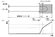
- FIG. 8A is a schematic diagram showing ion trajectories in the dual stage reflectron
- FIG. 8B is a schematic diagram of potential distribution on the central axis.
- the ion reflector is composed of a two-stage uniform electric field (an electric field whose potential is proportional to the distance) of the first stage part S1 and the second stage part S2, and the non-electric field drift part and 1 Ions pass through the boundary between the first stage uniform electric field (first stage part S1) and the boundary between the first stage uniform electric field and the second stage uniform electric field (second stage part S2).
- Grid electrodes G1 and G2 in which many possible openings are formed are provided. That is, the no-electric field drift part and the first stage part S1 are partitioned by the grid electrode G1, and the first stage part S1 and the second stage part S2 are partitioned by the grid electrode G2.
- the first stage part S1 is shorter than the second stage part S2, and when the ions lose about 2/3 of the initial energy in the first stage part S1, the total flight time spread is up to the second derivative of energy. Corrected (ie, second order energy convergence is achieved). For this reason, the spread of the flight time is reduced even with respect to the ion packet having the initial energy spread to some extent, and as a result, a high mass resolution is obtained.
- Such dual stage reflectrons are most widely used in commercially available time-of-flight mass spectrometers.
- the electric field is basically a uniform electric field in each stage of the ion reflector, but the electric potential distribution of this part of the electric field is appropriately corrected to obtain a non-uniform electric field. It is known that energy convergence can be improved by doing so.
- the inventors of the present application disclosed in Patent Document 1 that ions that fly on the central axis have energy exceeding a certain energy threshold by slightly correcting the potential distribution of the second stage portion S2 in the dual stage reflectron.
- a new TOFMS that realizes isochronism for packets is proposed.
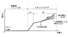
- FIG. 9 is a conceptual diagram of the potential distribution in the dual stage reflectron described in Patent Document 1.
- a position P in FIG. 9 is a secondary convergence position in a conventional dual stage reflectron in which no correction potential is superimposed.
- a correction potential Z C (U) proportional to ⁇ U (Z) ⁇ E 0 ⁇ 3.5 is applied to the potential Z A (U) by the uniform electric field.
- the correction potential Z C (U) is not superimposed, the spread of time of flight is compensated up to the second derivative of energy (the prior art Mamilyn solution), but the correction potential Z C (U) is superimposed.
- An ion reflector is generally configured to include a plurality of guard ring electrodes in order to form an ion reflection electric field in its internal space.
- FIG. 10 is a configuration diagram of a general ion reflector 4 including a plurality of guard ring electrodes.
- One guard ring electrode 401 is a substantially annular metal plate having an opening in the center. The shape of the opening varies depending on the shape of the ion trajectory, such as a circle or a rectangle.
- the thickness of one guard ring electrode 401 is Te, and an insulating spacer 402 having a thickness Ts is disposed between two adjacent guard ring electrodes 401. Therefore, the interval between two adjacent guard ring electrodes 401 is Ts.
- a guard ring electrode 401 and a spacer 402 having the same shape are used in the first stage portion S1 and the second stage portion S2. This is mainly for reducing the cost by sharing the guard ring electrode 401 and the spacer 402 with each other.
- Patent Document 2 describes a method of arranging guard ring electrodes with high positional accuracy and realizing them at low cost. In this document as well, it is assumed that the thicknesses of the plurality of guard ring electrodes are all the same, and the distance between adjacent electrodes, that is, the thickness of the spacer is also the same.
- guard ring electrodes As described above, in order to form a non-uniform ideal potential distribution along the central axis inside the ion reflector, as many guard ring electrodes as possible are arranged as closely as possible (that is, at the highest possible density). It is desirable to do.
- the guard ring electrode should be as thin as possible.
- the inner peripheral edge portion facing the central opening of the guard ring electrode is as close to the central axis as possible.
- the guard ring electrode has a rotationally symmetric shape with respect to the Z axis, and the diameter of the opening through which ions pass is 100 [mm].
- the applied voltage to each guard ring electrode is sequentially 0, 200, 400, 600, 800 from the incident end side electrode. 1000 [V].
- FIG. 11B is a calculation result of a potential distribution formed in the space inside the guard ring electrode, and equipotential surfaces are displayed at intervals of 20 [V].
- the cause of the potential shift described in (1) is the thickness of the guard ring electrode 401.
- the thinner the guard ring electrode 401 the smaller the potential shift amount at a position away from the central axis by a predetermined distance Y (if the guard ring electrode is infinitely thin, this shift does not occur).
- the guard ring electrode should be thin as long as it is thin.
- Grid electrodes G1 and G2 are provided at the boundary of, so as to form electric fields of different strengths on both sides across the boundary and allow ions to pass therethrough. If the grid electrodes G1 and G2 are bent or slack, they contribute to distortion of the potential distribution inside the ion reflector.
- Non-Patent Document 3 describes a method of stretching a grid electrode without slack.
- the guard ring electrode needs to have a certain thickness due to its structure.
- the thickness of the guard ring electrode is required to be about 5 to 10 mm or more.
- the thickness of the guard ring electrode is considerably less than about 2 mm. However, it is practically impossible to stretch the grid electrode at such a thickness. Also in such a gridless reflector, the same shape of the guard ring electrode and the spacer are commonly used in all, similarly to the above-described ion reflector with a grid.
- the thickness of the guard ring electrode is set to 10 [mm] in consideration of such circumstances, but as is clear from the above results, when the guard ring electrode becomes thicker to this extent, the radial direction particularly from the central axis The unevenness of the potential distribution at positions far away from each other becomes remarkable.
- the deviation between the actually obtained potential and the ideal potential becomes large, and the ion packet The decrease in isochronism with respect to is increased.
- the terms “thick electrode” and “thin electrode” are used as the guard ring electrode constituting the ion reflector.
- the “thick electrode” is 5 from the relationship with the prior art as described above.
- An electrode having a thickness of about ⁇ 10 mm or more is meant, while a “thin electrode” means an electrode having a thickness of about 2 [mm] or less.
- the present invention has been made in order to solve the above-mentioned problems, and its object is to provide a TOFMS including an ion reflector that can bring the reflected electric field to be formed closer to an ideal state while reducing the cost. Is to provide.
- the present invention which has been made to solve the above-described problems, includes an ion ejection unit that imparts constant energy to ions to be analyzed, an electric field ion drift unit for allowing ions to fly freely, and the electric field ion drift
- An ion reflector including a plurality of plate-like electrodes arranged along an ion trajectory so as to reflect and fold the ions flying through the section by the action of an electric field, and the no-field ion drift reflected by the ion reflector
- the ion flight space by the ion reflector includes a first region in which a decelerating electric field for decelerating ions passing through the no-field ion drift part is formed, and a reflected electric field for reflecting ions decelerated in the first region.
- the thickness of the plurality of electrodes arranged in the second region is made thinner than the thickness of the plurality of electrodes arranged in the first region.
- the reflected electric field formed in the second region may be an electric field that reflects ions decelerated by the decelerating electric field in the first region at a position corresponding to the initial energy of each ion.
- the thickness of all the guard ring electrodes constituting the ion reflector is the same, whereas in the TOFMS according to the present invention, it has only the action of decelerating ions.
- the thickness of the electrode is changed between the first region and the second region having the function of reflecting ions. In the first region, the electrode is thicker than the second region.
- the thickness of the plurality of electrodes arranged in the second region may be about 2 mm or less, and the thickness of the plurality of electrodes arranged in the first region may be 5 to 10 mm or more.
- the electrode (guard ring electrode) constituting the ion reflector when the electrode (guard ring electrode) constituting the ion reflector is thickened, the bend of the equipotential surface particularly at a position away from the central axis in the radial direction increases, and the deviation from the ideal potential increases. .
- the potential shift as described above in the first region in which only the ions are decelerated does not significantly affect the time convergence of ions, and the isochronism is substantially reduced. It will not be damaged.
- the above-described potential shift in the second region where ions are reflected greatly affects the time convergence of ions.
- the electrode (guard ring electrode) is thin in this second region.
- the first region of the no-field ion drift part and the ion reflector, and the first region and the second region of the ion reflector are each an ion reflector. It can be set as the structure divided by the grid
- this TOFMS is not a gridless reflectron but a grid-equipped reflectron, and by means of a grid electrode (grid electrode), an electric field ion drift portion, a first region of an ion reflector, and a first region of an ion reflector The second region is partitioned from each other, and the electric fields do not interfere with each other with the partition.
- a grid electrode grid electrode
- an electric field ion drift portion a first region of an ion reflector
- the second region is partitioned from each other, and the electric fields do not interfere with each other with the partition.
- the grid-like electrode that partitions the first region and the second region of the ion reflector has the same thickness (Te1) of the plurality of electrodes arranged in the first region and the same thickness of the plurality of electrodes arranged in the second region ( It is preferably stretched to an electrode having a thickness half of (Te2) ((Te1 / 2) + (Te2 / 2)), and the grid electrode is preferably stretched at a position Tf2 from the back of the reflector.
- the grid electrode may be stretched on an electrode that is thicker than the thin electrode disposed in the second region. Therefore, while using a thin electrode in the second region, the grid electrode can be stretched without bending or slack, and potential distribution distortion inside the ion reflector due to these can be avoided.
- the opening of the thick electrode disposed in the first region is further improved in order to further improve the mass resolution. May be wider than the opening of the thin electrode disposed in the second region.
- the member constituting the thick electrode arranged in the first region and the member constituting the thin electrode arranged in the second region may be made common. That is, a thick electrode disposed in the first region is formed by overlapping a plurality of thin electrodes disposed in the second region.
- a general-purpose processing technique such as etching or punching
- a thin electrode of the same shape can be produced in large quantities at a low cost from a thin and large metal plate. Therefore, if a thick electrode is formed using a thin electrode, the cost can be reduced as compared with a case where a thick electrode is manufactured by machining.
- spacers are arranged between adjacent electrodes among the electrodes constituting the ion reflector so that all the spacers have the same thickness. It is preferable that the electrode thickness and the electrode arrangement be adjusted. According to this configuration, since all the spacers can be made common, the manufacturing cost of the ion reflector can be reduced, and adjustment during assembly is facilitated.
- the electrodes arranged in the second region are thin, the electrodes can be arranged at a high density, and distortion of the equipotential surface due to the electrode thickness can be minimized.
- An ideal correction potential as described in Patent Document 1 can be formed. Thereby, the reflectron close to the ideal state can be realized, and high mass resolution can be realized. Further, by increasing the thickness of the electrodes arranged in the first region and widening the electrode interval, the number of electrodes arranged in the first region can be reduced. Even in such a case, since the device performance such as mass resolution can be secured by the potential correction in the second region, the cost can be reduced by reducing the number of electrodes within a range not affecting the performance.
- the schematic block diagram of TOFMS by one Example of this invention The figure which shows the electrode structure of the ion reflector in TOFMS of a present Example.
- FIG. 4 shows the center axis
- the schematic diagram (a) which shows the ion orbit in the dual stage type reflectron of a prior art, and the schematic diagram (b) of the electric potential distribution on a central axis.
- FIG. The block diagram of a general ion reflector.
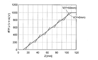
- Potential distribution by an ideal uniform electric field, and the potential distribution by the ideal uniform electric field on the Z axis and on a line parallel to the Z axis at Y 10, 20, 30, 40, 50 [mm].
- FIG. 14 is a diagram showing a simulation result of a relative time-of-flight spread dT / T with respect to a relative energy spread dU / U when ions fly on a central axis and a trajectory deviating from the central axis in the ion reflector having the structure shown in FIG. .
- FIG. 14 is a diagram showing an electrode structure of a conventional ion reflector assumed in the simulation. Since the ion reflector assumed here is a slit-shaped electrode having a plane-symmetric structure in the X-axis direction and mirror-symmetric with respect to the XZ plane, only the + Y direction including the XZ plane is shown in FIG. The electrode structure is depicted on the end face. The same applies to FIGS. 2 to 4 and 7 described later.
- the ion reflector has a configuration in which both the first stage portion S1 and the second stage portion S2 are guard ring electrodes having the same thickness, and the spacers are also made common in the same thickness.
- the length of the drift part is 1000 [mm]
- the length of the first stage part S1 is 100 [mm]
- the length of the second stage part S2 is 300 [mm].
- the slit-type opening width of the guard ring electrode is 40 [mm].
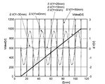
- Videal is an ideal potential distribution in which a correction potential is superimposed on a potential due to a uniform electric field
- ⁇ V is a distribution of potential deviation between the ideal potential and the actual potential.
- FIG. 16 shows a simulation of the relative time-of-flight spread dT / T with respect to the relative energy spread dU / U when ions fly on the central axis and on a trajectory deviating from the central axis in the ion reflector having the structure shown in FIG. It is a figure which shows a result.
- an ion having a relative energy spread dU / U of ⁇ 0.2 corresponds to an ion reflected at the secondary convergence position (correction potential start point), and ⁇ 0.2 ⁇ dU / U ⁇ 0.2.
- the cause of such a decrease in mass resolution is the thickness of the guard ring electrode in the ion reflection region (second stage portion S2 in this example). Therefore, in the present invention, the guard ring electrode is made thinner in the ion reflection region than in the prior art, so that the mass resolution is improved particularly for ions passing through a trajectory away from the central axis.
- FIG. 1 is a schematic configuration diagram of the TOFMS of the present embodiment
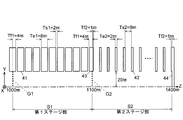
- FIG. 2 is a diagram illustrating an electrode structure of an ion reflector in the TOFMS of the present embodiment
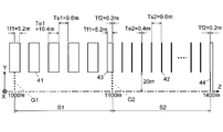
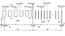
- FIGS. 3 and 4 are diagrams illustrating modifications of the electrode structure of the ion reflector. is there.
- sample-derived ions generated by the ion source 1 are introduced into the ion acceleration unit 2. Then, these ions are given initial energy by an electric field formed by a voltage applied to the ion acceleration unit 2 in a pulse manner from the acceleration voltage source 7 at a predetermined timing, and are sent to the flight space in the flight tube 3.
- an ion reflector 4 including a plurality of guard ring electrodes 41, 42, 43 and a termination electrode 44 disposed along the ion optical axis is installed.
- the first grid electrode G1 is stretched at the opening of the guard ring electrode 41 closest to the ion accelerating unit 2
- the second grid electrode G2 is stretched at the opening of another guard ring electrode 43. It is installed.
- a predetermined DC voltage is applied from the reflector DC voltage source 6 to each of the guard ring electrodes 41, 42, 43 and the termination electrode 44 constituting the ion reflector 4, whereby a predetermined potential is applied to the internal space of the ion reflector 4.
- An electrostatic field (DC electric field) having a shape is formed. Ions are reflected by the ion reflector 4 by the action of this electric field. The ions that are reflected and returned reach the detector 5, and the detector 5 outputs a detection signal corresponding to the amount of ions that have reached.
- the control unit 8 controls the acceleration voltage source 7, the reflector DC voltage source 6, and the like.
- the data processing unit 9 obtains ion acceleration timing information, that is, flight start time information from the control unit 8, and uses this as a reference to measure the flight time based on the detection signal of each ion.
- ion acceleration timing information that is, flight start time information from the control unit 8
- flight start time information from the control unit 8
- a mass spectrum is created in terms of mass to charge ratio m / z.
- the ion source 1 can be an ion source by any ionization method such as MALDI, ESI, APCI, EI, CI, depending on the form of the sample.
- the ion accelerator 2 may be a three-dimensional quadrupole ion trap or a linear ion trap. Further, when the ion source 1 is an ion source such as MALDI, the ion accelerator 2 may be a simple acceleration electrode that extracts and accelerates ions generated by the ion source 1. In order to suppress variations in initial energy of ions, an orthogonal acceleration method in which ions extracted from the ion source 1 are accelerated in a direction orthogonal to the extraction direction and sent to the flight tube 3 may be used.
- the ion acceleration part 2 can be comprised from an extrusion electrode and one or several grid electrodes.
- the guard ring electrode 41 disposed between the first grid electrode G1 and the second grid electrode G2 (that is, the first stage portion S1) including the leading guard ring electrode has a thickness Te1.
- the guard ring electrode 42 disposed between the second grid electrode G2 and the termination electrode 44 (that is, the second stage portion S2) has a thickness Te2 of 2 [mm]. is there. That is, in this example, the thickness Te1 of the guard ring electrode 41 disposed in the first stage portion S1 corresponding to the first region in the present invention is disposed in the second stage portion S2 corresponding to the second region in the present invention.
- the guard ring electrode 42 is four times the thickness Te2, the former being a so-called thick electrode and the latter corresponding to a thin electrode.
- the slit-type opening width of the guard ring electrodes 41, 42, 43 is 40 [mm].
- the second grid electrode G2 is attached at a position of 4 mm from the end of the guard ring electrode 43 on the first stage portion S1 side, and faces the first stage portion S1 with the second grid electrode G2 interposed therebetween (included).
- the thickness of the portion facing (included) the second stage portion S2 is 1 [mm].
- the guard ring electrode 42 arranged on the second stage portion S2 is considerably thinner than the conventional general thickness of 5 to 10 [mm], so that it is separated from the central axis in the radial direction. Even at the same position, the bend of the equipotential surface is small, thereby reducing the spread of flight time.
- the conventional configuration shown in FIG. As described above, the spacers inserted between the guard ring electrodes cannot be shared. That will lead to increased costs. Therefore, as an improved version of the configuration shown in FIG. 2, the pitch of the guard ring electrode and the thickness of the guard ring electrode are adjusted in each of the first stage portion S1 and the second stage portion S2, as shown in FIG. This is a configuration of a modified example.
- the electrode pitch of the guard ring electrodes 41 arranged in the first stage portion S1 is increased to 20 [mm]
- spacers of the same size can be used as all spacers, so that the cost can be reduced compared to the configuration of FIG. 2 that requires two types of spacers having different sizes.
- the number of guard ring electrodes 41 arranged on the first stage portion S1 is reduced from nine to four, and the number of electrodes that need to be processed with high accuracy is reduced, which contributes to cost reduction. .
- the guard ring electrode 41 disposed on the first stage portion S1 is further thickened, the unevenness of the potential on the central axis in the first stage portion S1 becomes large.
- the potential unevenness in the first stage portion S1 has little influence on the overall isochronism, in consideration of realizing higher isochronism, in the first stage portion S1, in practice. It is better to suppress the unevenness of the potential as much as possible. Therefore, as a further improved version of the configuration shown in FIG. 3, the central opening of the guard ring electrode 41 disposed in the first stage portion S1 is enlarged in the configuration of the modification shown in FIG.
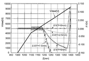
- 15 is a diagram showing the simulation results of the potential distribution, and as in FIG. 15, V ideal is an ideal potential distribution in which a correction potential is superimposed on a potential by an ideal uniform electric field, and ⁇ V is an ideal potential. This is the distribution of potential deviation from the actual potential.
- FIG. 15 is a diagram showing the simulation results of the potential distribution, and as in FIG. 15, V ideal is an ideal potential distribution in which a correction potential is superimposed on a potential by an ideal uniform electric field, and ⁇ V is an ideal potential. This is the distribution of potential deviation from the actual potential.
- FIG. 15 is a diagram showing the simulation results of the potential distribution, and as in FIG. 15, V ideal is an ideal potential distribution in which a correction potential is superimposed on a potential by an ideal uniform electric field, and
- FIG. 6 shows the relative time-of-flight spread dT / T with respect to the relative energy spread dU / U in the case of ions flying on the central axis and on a trajectory deviating from the central axis in the ion reflector according to the modification shown in FIG. It is a figure which shows a simulation result.
- the ion reflector according to the present embodiment has a small potential unevenness in the second stage portion S2, but instead has a large potential unevenness in the first stage portion S1. Become. This is an influence of the guard ring electrode 41 disposed on the first stage portion S1 being thick.
- the unevenness of the potential in the first stage portion S1 is large, for example, the spread of the flight time of ions flying on the central axis hardly increases. . From this, it can be concluded that the unevenness of the potential of the first stage portion S1 does not greatly affect isochronism.
- the ideal potential distribution is formed by introducing the non-uniform electric field to the second stage portion S2 using the method described in Patent Document 1, but only the uniform electric field is formed. Even if the present invention is applied to TOFMS using a conventional ion reflector, there is a sufficient advantage.
- the conventional dual stage type (or more multistage type) ion reflector that forms a uniform electric field it is the same that the unevenness of the potential must be suppressed in the ion reflection region in order to increase the mass resolution. Therefore, in the conventional ion reflector, a region near the central axis where the unevenness of the potential is sufficiently small is used as the ion flight space.
- the thinner the guard ring electrode the wider the region near the central axis where the unevenness of the potential is sufficiently small, so by using a thin electrode as the guard ring electrode disposed in the region where ions are reflected, The diameter of the ion reflector can be reduced and the overall size of the apparatus can be advantageously reduced.
- the opening shape of the guard ring electrode of the ion reflector is a round hole or an infinitely long slit shape, but not limited thereto, a guard ring electrode having a rectangular shape or a long hole shape is not limited thereto. It can also be used.
- a guard whose opening shape is a rectangular shape or a long hole shape It is more convenient to use a ring electrode because a wide space region capable of achieving high mass resolution can be secured in one direction. Even in this case, the same good performance as in the case of the guard ring electrode whose opening shape is a round hole or an infinitely long slit shape can be achieved.
- the above simulation is an example in which the present invention is applied to a dual-stage reflectron, but the present invention can also be applied to an ion reflector having three or more stages.
- the final stage is an ion reflection region, and the others are ion deceleration regions.
Landscapes
- Chemical & Material Sciences (AREA)
- Analytical Chemistry (AREA)
- Other Investigation Or Analysis Of Materials By Electrical Means (AREA)
Description
(1)図12及び図13から、イオンリフレクタの中心軸(Y=0)付近では、実際の電位分布は一様電場による理想的な電位に近いものの、中心軸から外れてガードリング電極401に近づくほど(つまりYが大きいほど)、理想電位と実際の電位とのずれは大きくなる。
(2)図11(b)に示すように、ガードリング電極401に近づくほど等電位面の曲がりが大きくなっている。ガードリング電極401が薄ければ、この曲がりの程度が緩和されることは明らかであるから、(1)で述べた電位のずれの原因はガードリング電極401の厚みであることが判る。換言すれば、ガードリング電極401が薄いほど、中心軸から所定の距離Yだけ離れた位置における電位のずれ量は小さくなる(ガードリング電極が無限に薄ければこのずれは無い)と考えられる。
前記イオンリフレクタによるイオンの飛行空間は、前記無電場イオンドリフト部を通り抜けて来たイオンを減速させる減速電場が形成される第1領域と、該第1領域で減速されたイオンを反射させる反射電場が形成される第2領域とに区分され、前記第2領域に配置される複数の電極の厚さを前記第1領域に配置される複数の電極の厚さに比べて薄くしたことを特徴としている。
なお、本発明において、第2領域に形成される反射電場は、第1領域における減速電場で減速されたイオンをその各イオンの初期エネルギに応じた位置で反射させるような電場であればよい。
なお、図7の例では、厚さが0.4[mm]である金属板を電極41b、42ともに利用したが、金属板の厚さを0.2[mm]とすることで、電極43bや終端電極44における厚さTf2の部分の金属板部材も共通化することができる。
2…イオン加速部
3…フライトチューブ
4…イオンリフレクタ
41、42、43、41b、43b…ガードリング電極
44…終端電極
5…検出器
6…リフレクタ直流電圧源
7…加速電圧源
8…制御部
9…データ処理部
G、G1、G2…グリッド電極
S1…第1ステージ部
S2…第2ステージ部
Claims (8)
- 分析対象であるイオンに一定のエネルギを付与するイオン射出部と、イオンを自由に飛行させるための無電場イオンドリフト部と、該無電場イオンドリフト部を飛行して来たイオンを電場の作用により反射して折り返すべくイオン軌道に沿って複数配設された板状の電極を含むイオンリフレクタと、該イオンリフレクタで反射されて前記無電場イオンドリフト部を経て戻って来たイオンを検出する検出器と、を具備する飛行時間型質量分析装置において、
前記イオンリフレクタによるイオンの飛行空間は、前記無電場イオンドリフト部を通り抜けて来たイオンを減速させる減速電場が形成される第1領域と、該第1領域で減速されたイオンを反射させる反射電場が形成される第2領域とに区分され、前記第2領域に配置される複数の電極の厚さを前記第1領域に配置される複数の電極の厚さに比べて薄くしたことを特徴とする飛行時間型質量分析装置。 - 分析対象であるイオンに一定のエネルギを付与するイオン射出部と、イオンを自由に飛行させるための無電場イオンドリフト部と、該無電場イオンドリフト部を飛行して来たイオンを電場の作用により反射して折り返すべくイオン軌道に沿って複数配設された板状の電極を含むイオンリフレクタと、該イオンリフレクタで反射されて前記無電場イオンドリフト部を経て戻って来たイオンを検出する検出器と、を具備する飛行時間型質量分析装置において、
前記イオンリフレクタによるイオンの飛行空間は、前記無電場イオンドリフト部を通り抜けて来たイオンを減速させる減速電場が形成される第1領域と、該第1領域で減速されたイオンを反射させる反射電場が形成される第2領域とに区分され、前記第2領域に配置される複数の電極の厚さは略2mm以下、前記第1領域に配置される複数の電極の厚さは5~10mmの範囲又はそれ以上、であることを特徴とする飛行時間型質量分析装置。 - 請求項1又は2に記載の飛行時間型質量分析装置において、
前記無電場イオンドリフト部と前記イオンリフレクタの第1領域、及び、該イオンリフレクタの第1領域と第2領域は、それぞれイオンリフレクタを構成する電極の開口に張設された格子状電極により仕切られてなることを特徴とする飛行時間型質量分析装置。 - 請求項3に記載の飛行時間型質量分析装置において、
前記無電場イオンドリフト部と前記イオンリフレクタの第1領域とを仕切る格子状電極は前記第1領域に配置される最初の複数に張設され、該電極の厚さは該第1領域に配置される同一厚さの他の複数の電極の厚さの1/2以上であり、
前記イオンリフレクタの第1領域と第2領域とを仕切る格子状電極は、該第1領域に配置される複数の同一厚さの電極の厚さの1/2と該第2領域に配置される複数の同一厚さの電極の厚さの1/2との和に等しい厚さを有する電極に張設されてなることを特徴とする飛行時間型質量分析装置。 - 請求項1~4のいずれかに記載の飛行時間型質量分析装置において、
前記第1領域に配置される厚い電極の開口を前記第2領域に配置される薄い電極の開口よりも広くしたことを特徴とする飛行時間型質量分析装置。 - 請求項1~5のいずれかに記載の飛行時間型質量分析装置において、
前記イオンリフレクタを構成する電極の中で隣接する電極の間にはスペーサが配置されてなり、全てのスペーサの厚さが同一であるように電極の厚さ及び電極の配置が調整されてなることを特徴とする飛行時間型質量分析装置。 - 請求項1~6のいずれかに記載の飛行時間型質量分析装置において、
前記第1領域に配置される厚い電極は、前記第2領域に配置される薄い電極を複数重ねることで形成されてなることを特徴とする飛行時間型質量分析装置。 - 請求項1~7のいずれかに記載の飛行時間型質量分析装置において、
前記第1領域に配置される複数の電極のピッチが、前記第2領域に配置される複数の電極のピッチと比べて広く、該第2領域に比べて第1領域では単位長さ当りの電極数が少なくなっていることを特徴とする飛行時間型質量分析装置。
Priority Applications (4)
| Application Number | Priority Date | Filing Date | Title |
|---|---|---|---|
| US14/434,596 US9490114B2 (en) | 2012-10-10 | 2013-09-18 | Time-of-flight mass spectrometer |
| CN201380053113.1A CN104704604B (zh) | 2012-10-10 | 2013-09-18 | 飞行时间质谱仪 |
| EP13846026.6A EP2908329B1 (en) | 2012-10-10 | 2013-09-18 | Time-of-flight mass spectrometer |
| JP2014540789A JP5862791B2 (ja) | 2012-10-10 | 2013-09-18 | 飛行時間型質量分析装置 |
Applications Claiming Priority (2)
| Application Number | Priority Date | Filing Date | Title |
|---|---|---|---|
| JP2012224832 | 2012-10-10 | ||
| JP2012-224832 | 2012-10-10 |
Publications (1)
| Publication Number | Publication Date |
|---|---|
| WO2014057777A1 true WO2014057777A1 (ja) | 2014-04-17 |
Family
ID=50477248
Family Applications (1)
| Application Number | Title | Priority Date | Filing Date |
|---|---|---|---|
| PCT/JP2013/075102 Ceased WO2014057777A1 (ja) | 2012-10-10 | 2013-09-18 | 飛行時間型質量分析装置 |
Country Status (5)
| Country | Link |
|---|---|
| US (1) | US9490114B2 (ja) |
| EP (1) | EP2908329B1 (ja) |
| JP (1) | JP5862791B2 (ja) |
| CN (1) | CN104704604B (ja) |
| WO (1) | WO2014057777A1 (ja) |
Cited By (4)
| Publication number | Priority date | Publication date | Assignee | Title |
|---|---|---|---|---|
| GB2516742A (en) * | 2013-06-07 | 2015-02-04 | Micromass Ltd | Method of generating electric field for manipulating charged particles |
| US10186413B2 (en) | 2014-12-24 | 2019-01-22 | Shimadzu Corporation | Time-of-flight mass spectrometer |
| CN111902908A (zh) * | 2018-04-20 | 2020-11-06 | 英国质谱公司 | 具有平滑场的无栅格离子反射镜 |
| JP2023125833A (ja) * | 2022-02-28 | 2023-09-07 | 株式会社島津製作所 | 飛行時間型質量分析装置 |
Families Citing this family (19)
| Publication number | Priority date | Publication date | Assignee | Title |
|---|---|---|---|---|
| CA2913654C (en) * | 2013-06-07 | 2022-06-14 | Micromass Uk Limited | Method of generating electric field for manipulating charged particles |
| CN107240543B (zh) * | 2017-07-26 | 2023-06-27 | 合肥美亚光电技术股份有限公司 | 一种带有双场加速区的飞行时间质谱仪 |
| EP3662501A1 (en) | 2017-08-06 | 2020-06-10 | Micromass UK Limited | Ion mirror for multi-reflecting mass spectrometers |
| US11817303B2 (en) | 2017-08-06 | 2023-11-14 | Micromass Uk Limited | Accelerator for multi-pass mass spectrometers |
| GB2568354B (en) * | 2017-09-28 | 2022-08-10 | Bruker Daltonics Gmbh & Co Kg | Wide-range high mass resolution in reflector time-of-flight mass spectrometers |
| GB201807626D0 (en) | 2018-05-10 | 2018-06-27 | Micromass Ltd | Multi-reflecting time of flight mass analyser |
| WO2019220553A1 (ja) * | 2018-05-16 | 2019-11-21 | 株式会社島津製作所 | 飛行時間型質量分析装置 |
| GB201808530D0 (en) | 2018-05-24 | 2018-07-11 | Verenchikov Anatoly | TOF MS detection system with improved dynamic range |
| GB201808949D0 (en) | 2018-05-31 | 2018-07-18 | Micromass Ltd | Bench-top time of flight mass spectrometer |
| GB201808912D0 (en) | 2018-05-31 | 2018-07-18 | Micromass Ltd | Bench-top time of flight mass spectrometer |
| GB201808893D0 (en) * | 2018-05-31 | 2018-07-18 | Micromass Ltd | Bench-top time of flight mass spectrometer |
| WO2019229469A1 (en) | 2018-05-31 | 2019-12-05 | Micromass Uk Limited | Mass spectrometer |
| GB201808932D0 (en) | 2018-05-31 | 2018-07-18 | Micromass Ltd | Bench-top time of flight mass spectrometer |
| GB201810573D0 (en) | 2018-06-28 | 2018-08-15 | Verenchikov Anatoly | Multi-pass mass spectrometer with improved duty cycle |
| CN110706999A (zh) * | 2018-07-24 | 2020-01-17 | 宁波海歌电器有限公司 | 一种双通道飞行时间质量分析器 |
| GB201903779D0 (en) | 2019-03-20 | 2019-05-01 | Micromass Ltd | Multiplexed time of flight mass spectrometer |
| CN112885701B (zh) * | 2021-02-26 | 2022-02-11 | 中国科学院化学研究所 | 一种离子过滤装置及方法 |
| WO2022238953A2 (en) * | 2021-05-14 | 2022-11-17 | Dh Technologies Development Pte. Ltd. | Ion mirror for time-of-flight mass spectrometer |
| JP7533393B2 (ja) * | 2021-07-21 | 2024-08-14 | 株式会社島津製作所 | 直交加速飛行時間型質量分析装置 |
Citations (5)
| Publication number | Priority date | Publication date | Assignee | Title |
|---|---|---|---|---|
| JP2002502096A (ja) * | 1998-01-30 | 2002-01-22 | シマヅ リサーチ ラボラトリー(ヨーロッパ)リミティド | 飛行時間型質量分析装置 |
| US6849846B2 (en) | 2002-08-23 | 2005-02-01 | Agilent Technologies, Inc. | Precision multiple electrode ion mirror |
| JP3797200B2 (ja) * | 2001-11-09 | 2006-07-12 | 株式会社島津製作所 | 飛行時間型質量分析装置 |
| WO2012033094A1 (ja) * | 2010-09-08 | 2012-03-15 | 株式会社島津製作所 | 飛行時間型質量分析装置 |
| WO2012086630A1 (ja) | 2010-12-20 | 2012-06-28 | 国立大学法人神戸大学 | 飛行時間型質量分析装置 |
Family Cites Families (12)
| Publication number | Priority date | Publication date | Assignee | Title |
|---|---|---|---|---|
| DE3524536A1 (de) * | 1985-07-10 | 1987-01-22 | Bruker Analytische Messtechnik | Flugzeit-massenspektrometer mit einem ionenreflektor |
| DE3920566A1 (de) * | 1989-06-23 | 1991-01-10 | Bruker Franzen Analytik Gmbh | Ms-ms-flugzeit-massenspektrometer |
| US5814813A (en) * | 1996-07-08 | 1998-09-29 | The Johns Hopkins University | End cap reflection for a time-of-flight mass spectrometer and method of using the same |
| DE10005698B4 (de) * | 2000-02-09 | 2007-03-01 | Bruker Daltonik Gmbh | Gitterloses Reflektor-Flugzeitmassenspektrometer für orthogonalen Ioneneinschuss |
| GB0100862D0 (en) | 2001-01-11 | 2001-02-21 | Scient Analysis Instr Ltd | Reflactron |
| DE10156604A1 (de) * | 2001-11-17 | 2003-05-28 | Bruker Daltonik Gmbh | Raumwinkelfokussierender Reflektor für Flugzeitmassenspektrometer |
| US6924480B2 (en) * | 2002-02-26 | 2005-08-02 | The Regents Of The University Of California | Apparatus and method for using a volume conductive electrode with ion optical elements for a time-of-flight mass spectrometer |
| GB0311567D0 (en) * | 2003-05-16 | 2003-06-25 | Micromass Ltd | Mass spectrometer |
| GB2426120A (en) * | 2005-05-11 | 2006-11-15 | Polaron Plc | A reflectron for use in a three-dimensional atom probe |
| EP2355129B1 (de) * | 2010-01-29 | 2013-01-09 | Helmholtz-Zentrum Geesthacht Zentrum für Material- und Küstenforschung GmbH | Reflektor für ein Flugzeitmassenspektrometer |
| DE102010039030A1 (de) | 2010-08-06 | 2012-02-09 | Humboldt-Universität Zu Berlin | Reflektron mit alternierenden Elektrodendicken sowie Flugzeitmassenspektrometer mit einem erfindungsgemäßen Reflektron |
| CN103907171B (zh) * | 2011-10-28 | 2017-05-17 | 莱克公司 | 静电离子镜 |
-
2013
- 2013-09-18 WO PCT/JP2013/075102 patent/WO2014057777A1/ja not_active Ceased
- 2013-09-18 EP EP13846026.6A patent/EP2908329B1/en active Active
- 2013-09-18 JP JP2014540789A patent/JP5862791B2/ja active Active
- 2013-09-18 US US14/434,596 patent/US9490114B2/en active Active
- 2013-09-18 CN CN201380053113.1A patent/CN104704604B/zh active Active
Patent Citations (5)
| Publication number | Priority date | Publication date | Assignee | Title |
|---|---|---|---|---|
| JP2002502096A (ja) * | 1998-01-30 | 2002-01-22 | シマヅ リサーチ ラボラトリー(ヨーロッパ)リミティド | 飛行時間型質量分析装置 |
| JP3797200B2 (ja) * | 2001-11-09 | 2006-07-12 | 株式会社島津製作所 | 飛行時間型質量分析装置 |
| US6849846B2 (en) | 2002-08-23 | 2005-02-01 | Agilent Technologies, Inc. | Precision multiple electrode ion mirror |
| WO2012033094A1 (ja) * | 2010-09-08 | 2012-03-15 | 株式会社島津製作所 | 飛行時間型質量分析装置 |
| WO2012086630A1 (ja) | 2010-12-20 | 2012-06-28 | 国立大学法人神戸大学 | 飛行時間型質量分析装置 |
Non-Patent Citations (4)
| Title |
|---|
| B.A. MAMYRIN: "The mass-reflectron, a new nonmagnetic time-of-flight mass spectrometer with high resolution", SOV. PHYS. -JETP, vol. 37, 1973, pages 45 - 48 |
| R. J COTTER: "Time-of-Flight Mass Spectrometry: Instrumentation and Applications in Biological Research", 1997, AMERICAN CHEMICAL SOCIETY |
| See also references of EP2908329A4 |
| T. BERGMANN: "High resolution time-of-flight mass spectrometers. Part III. Reflector design", REVIEW OF SCIENTIFIC INSTRUMENTS, vol. 61, no. 10, 1990, pages 2592 - 2600 |
Cited By (7)
| Publication number | Priority date | Publication date | Assignee | Title |
|---|---|---|---|---|
| GB2516742A (en) * | 2013-06-07 | 2015-02-04 | Micromass Ltd | Method of generating electric field for manipulating charged particles |
| GB2516742B (en) * | 2013-06-07 | 2016-01-13 | Micromass Ltd | Method of generating electric field for manipulating charged particles |
| US10186413B2 (en) | 2014-12-24 | 2019-01-22 | Shimadzu Corporation | Time-of-flight mass spectrometer |
| CN111902908A (zh) * | 2018-04-20 | 2020-11-06 | 英国质谱公司 | 具有平滑场的无栅格离子反射镜 |
| CN111902908B (zh) * | 2018-04-20 | 2023-07-25 | 英国质谱公司 | 具有平滑场的无栅格离子反射镜 |
| JP2023125833A (ja) * | 2022-02-28 | 2023-09-07 | 株式会社島津製作所 | 飛行時間型質量分析装置 |
| JP7750139B2 (ja) | 2022-02-28 | 2025-10-07 | 株式会社島津製作所 | 飛行時間型質量分析装置 |
Also Published As
| Publication number | Publication date |
|---|---|
| JP5862791B2 (ja) | 2016-02-16 |
| EP2908329B1 (en) | 2022-01-12 |
| CN104704604B (zh) | 2016-12-28 |
| EP2908329A1 (en) | 2015-08-19 |
| EP2908329A4 (en) | 2015-10-21 |
| US9490114B2 (en) | 2016-11-08 |
| JPWO2014057777A1 (ja) | 2016-09-05 |
| US20150270115A1 (en) | 2015-09-24 |
| CN104704604A (zh) | 2015-06-10 |
Similar Documents
| Publication | Publication Date | Title |
|---|---|---|
| JP5862791B2 (ja) | 飛行時間型質量分析装置 | |
| US9281175B2 (en) | First and second order focusing using field free regions in time-of-flight | |
| JP6287419B2 (ja) | 飛行時間型質量分析装置 | |
| US10964520B2 (en) | Multi-reflection mass spectrometer | |
| Radionova et al. | In pursuit of resolution in time‐of‐flight mass spectrometry: A historical perspective | |
| US11621156B2 (en) | Multi-reflecting time of flight mass analyser | |
| US9136101B2 (en) | Multi-reflection mass spectrometer | |
| US7326925B2 (en) | Multi-reflecting time-of-flight mass spectrometer with isochronous curved ion interface | |
| JP4939138B2 (ja) | 質量分析装置用イオン光学系の設計方法 | |
| US9136102B2 (en) | Multi-reflection mass spectrometer | |
| JP6292319B2 (ja) | 飛行時間型質量分析装置 | |
| US7355168B2 (en) | Time of flight mass spectrometer | |
| US9576782B2 (en) | Orthogonal acceleration system for time-of-flight mass spectrometer |
Legal Events
| Date | Code | Title | Description |
|---|---|---|---|
| 121 | Ep: the epo has been informed by wipo that ep was designated in this application |
Ref document number: 13846026 Country of ref document: EP Kind code of ref document: A1 |
|
| ENP | Entry into the national phase |
Ref document number: 2014540789 Country of ref document: JP Kind code of ref document: A |
|
| WWE | Wipo information: entry into national phase |
Ref document number: 14434596 Country of ref document: US |
|
| NENP | Non-entry into the national phase |
Ref country code: DE |
|
| WWE | Wipo information: entry into national phase |
Ref document number: 2013846026 Country of ref document: EP |