WO2014102994A1 - 炭化珪素半導体装置及びその製造方法 - Google Patents
炭化珪素半導体装置及びその製造方法 Download PDFInfo
- Publication number
- WO2014102994A1 WO2014102994A1 PCT/JP2012/084017 JP2012084017W WO2014102994A1 WO 2014102994 A1 WO2014102994 A1 WO 2014102994A1 JP 2012084017 W JP2012084017 W JP 2012084017W WO 2014102994 A1 WO2014102994 A1 WO 2014102994A1
- Authority
- WO
- WIPO (PCT)
- Prior art keywords
- trench
- layer
- silicon carbide
- semiconductor device
- drift layer
- Prior art date
- Legal status (The legal status is an assumption and is not a legal conclusion. Google has not performed a legal analysis and makes no representation as to the accuracy of the status listed.)
- Ceased
Links
Images








Classifications
-
- H—ELECTRICITY
- H10—SEMICONDUCTOR DEVICES; ELECTRIC SOLID-STATE DEVICES NOT OTHERWISE PROVIDED FOR
- H10D—INORGANIC ELECTRIC SEMICONDUCTOR DEVICES
- H10D30/00—Field-effect transistors [FET]
- H10D30/60—Insulated-gate field-effect transistors [IGFET]
- H10D30/64—Double-diffused metal-oxide semiconductor [DMOS] FETs
- H10D30/66—Vertical DMOS [VDMOS] FETs
- H10D30/665—Vertical DMOS [VDMOS] FETs having edge termination structures
-
- H—ELECTRICITY
- H10—SEMICONDUCTOR DEVICES; ELECTRIC SOLID-STATE DEVICES NOT OTHERWISE PROVIDED FOR
- H10D—INORGANIC ELECTRIC SEMICONDUCTOR DEVICES
- H10D30/00—Field-effect transistors [FET]
- H10D30/01—Manufacture or treatment
- H10D30/021—Manufacture or treatment of FETs having insulated gates [IGFET]
- H10D30/028—Manufacture or treatment of FETs having insulated gates [IGFET] of double-diffused metal oxide semiconductor [DMOS] FETs
- H10D30/0291—Manufacture or treatment of FETs having insulated gates [IGFET] of double-diffused metal oxide semiconductor [DMOS] FETs of vertical DMOS [VDMOS] FETs
- H10D30/0297—Manufacture or treatment of FETs having insulated gates [IGFET] of double-diffused metal oxide semiconductor [DMOS] FETs of vertical DMOS [VDMOS] FETs using recessing of the gate electrodes, e.g. to form trench gate electrodes
-
- H—ELECTRICITY
- H10—SEMICONDUCTOR DEVICES; ELECTRIC SOLID-STATE DEVICES NOT OTHERWISE PROVIDED FOR
- H10D—INORGANIC ELECTRIC SEMICONDUCTOR DEVICES
- H10D30/00—Field-effect transistors [FET]
- H10D30/60—Insulated-gate field-effect transistors [IGFET]
- H10D30/64—Double-diffused metal-oxide semiconductor [DMOS] FETs
- H10D30/66—Vertical DMOS [VDMOS] FETs
- H10D30/668—Vertical DMOS [VDMOS] FETs having trench gate electrodes, e.g. UMOS transistors
-
- H—ELECTRICITY
- H10—SEMICONDUCTOR DEVICES; ELECTRIC SOLID-STATE DEVICES NOT OTHERWISE PROVIDED FOR
- H10D—INORGANIC ELECTRIC SEMICONDUCTOR DEVICES
- H10D62/00—Semiconductor bodies, or regions thereof, of devices having potential barriers
- H10D62/10—Shapes, relative sizes or dispositions of the regions of the semiconductor bodies; Shapes of the semiconductor bodies
- H10D62/13—Semiconductor regions connected to electrodes carrying current to be rectified, amplified or switched, e.g. source or drain regions
- H10D62/149—Source or drain regions of field-effect devices
- H10D62/151—Source or drain regions of field-effect devices of IGFETs
- H10D62/156—Drain regions of DMOS transistors
- H10D62/157—Impurity concentrations or distributions
-
- H—ELECTRICITY
- H10—SEMICONDUCTOR DEVICES; ELECTRIC SOLID-STATE DEVICES NOT OTHERWISE PROVIDED FOR
- H10D—INORGANIC ELECTRIC SEMICONDUCTOR DEVICES
- H10D62/00—Semiconductor bodies, or regions thereof, of devices having potential barriers
- H10D62/80—Semiconductor bodies, or regions thereof, of devices having potential barriers characterised by the materials
- H10D62/83—Semiconductor bodies, or regions thereof, of devices having potential barriers characterised by the materials being Group IV materials, e.g. B-doped Si or undoped Ge
- H10D62/832—Semiconductor bodies, or regions thereof, of devices having potential barriers characterised by the materials being Group IV materials, e.g. B-doped Si or undoped Ge being Group IV materials comprising two or more elements, e.g. SiGe
- H10D62/8325—Silicon carbide
-
- H—ELECTRICITY
- H10—SEMICONDUCTOR DEVICES; ELECTRIC SOLID-STATE DEVICES NOT OTHERWISE PROVIDED FOR
- H10D—INORGANIC ELECTRIC SEMICONDUCTOR DEVICES
- H10D64/00—Electrodes of devices having potential barriers
- H10D64/01—Manufacture or treatment
-
- H—ELECTRICITY
- H10—SEMICONDUCTOR DEVICES; ELECTRIC SOLID-STATE DEVICES NOT OTHERWISE PROVIDED FOR
- H10D—INORGANIC ELECTRIC SEMICONDUCTOR DEVICES
- H10D64/00—Electrodes of devices having potential barriers
- H10D64/20—Electrodes characterised by their shapes, relative sizes or dispositions
- H10D64/27—Electrodes not carrying the current to be rectified, amplified, oscillated or switched, e.g. gates
- H10D64/311—Gate electrodes for field-effect devices
- H10D64/411—Gate electrodes for field-effect devices for FETs
- H10D64/511—Gate electrodes for field-effect devices for FETs for IGFETs
- H10D64/514—Gate electrodes for field-effect devices for FETs for IGFETs characterised by the insulating layers
- H10D64/516—Gate electrodes for field-effect devices for FETs for IGFETs characterised by the insulating layers the thicknesses being non-uniform
-
- H—ELECTRICITY
- H10—SEMICONDUCTOR DEVICES; ELECTRIC SOLID-STATE DEVICES NOT OTHERWISE PROVIDED FOR
- H10D—INORGANIC ELECTRIC SEMICONDUCTOR DEVICES
- H10D62/00—Semiconductor bodies, or regions thereof, of devices having potential barriers
- H10D62/10—Shapes, relative sizes or dispositions of the regions of the semiconductor bodies; Shapes of the semiconductor bodies
- H10D62/17—Semiconductor regions connected to electrodes not carrying current to be rectified, amplified or switched, e.g. channel regions
- H10D62/393—Body regions of DMOS transistors or IGBTs
-
- H—ELECTRICITY
- H10—SEMICONDUCTOR DEVICES; ELECTRIC SOLID-STATE DEVICES NOT OTHERWISE PROVIDED FOR
- H10D—INORGANIC ELECTRIC SEMICONDUCTOR DEVICES
- H10D64/00—Electrodes of devices having potential barriers
- H10D64/01—Manufacture or treatment
- H10D64/011—Manufacture or treatment of electrodes ohmically coupled to a semiconductor
- H10D64/0111—Manufacture or treatment of electrodes ohmically coupled to a semiconductor to Group IV semiconductors
- H10D64/0115—Manufacture or treatment of electrodes ohmically coupled to a semiconductor to Group IV semiconductors to silicon carbide
-
- H—ELECTRICITY
- H10—SEMICONDUCTOR DEVICES; ELECTRIC SOLID-STATE DEVICES NOT OTHERWISE PROVIDED FOR
- H10D—INORGANIC ELECTRIC SEMICONDUCTOR DEVICES
- H10D64/00—Electrodes of devices having potential barriers
- H10D64/01—Manufacture or treatment
- H10D64/013—Manufacture or treatment of electrodes having a conductor capacitively coupled to a semiconductor by an insulator
- H10D64/01366—Manufacture or treatment of electrodes having a conductor capacitively coupled to a semiconductor by an insulator the semiconductor being silicon carbide
-
- H—ELECTRICITY
- H10—SEMICONDUCTOR DEVICES; ELECTRIC SOLID-STATE DEVICES NOT OTHERWISE PROVIDED FOR
- H10D—INORGANIC ELECTRIC SEMICONDUCTOR DEVICES
- H10D64/00—Electrodes of devices having potential barriers
- H10D64/60—Electrodes characterised by their materials
- H10D64/62—Electrodes ohmically coupled to a semiconductor
Definitions
- the present invention relates to a silicon carbide semiconductor device and a method for manufacturing the same.
- FIG. 3 is an explanatory diagram of the off state.
- the depletion layer in the drift layer 10 mainly relaxes the high electric field.
- the silicon oxide film constituting the gate insulating film 1 has a dielectric constant of about 4 and lower than 4H—SiC 9.7, and the electric field strength is 2.4 in SiC according to the ratio of the dielectric constant.
- the gate insulating film at the bottom of the trench where the electric field is concentrated becomes a weak point.
- SiC is made amorphous by selectively injecting nitrogen ions into the bottom of the trench so that the trench bottom is oxidized at a high speed.
- an oxide film thicker than the side surface of the trench can be formed at the bottom of the trench.
- nitrogen ions having an implantation energy of a maximum of 380 KeV are implanted perpendicularly to the wafer so as to form a box profile with a depth of 0.5 ⁇ m at a concentration of 10 20 cm ⁇ 3 .
- Patent Document 1 if the ion is implanted to be amorphous, the oxidation rate is improved.
- the rate of oxidation is not sufficient with nitrogen ion implantation.
- An object of the present invention is to provide a high breakdown voltage trench type SiC-MOSFET that can be efficiently manufactured.
- the present invention includes a plurality of inventions that solve the above-described problems.
- phosphorus is added to the bottom surface of the trench after the trench formation step and before the oxidation step of oxidizing SiC to form a gate oxide film. Inject.
- a high breakdown voltage trench SiC-MOSFET that can be manufactured efficiently can be manufactured.
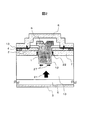
- FIG. 3 is an explanatory diagram showing an implementation method of Example 1. It is sectional drawing of conventional trench type MOSFET. It is explanatory drawing of the OFF state of conventional trench type MOSFET. It is sectional drawing of 2 step
- FIG. 6 is an explanatory diagram of a process flow for manufacturing the element of Example 1;
- FIG. 6 is an explanatory diagram of a process flow for manufacturing the element of Example 1;
- FIG. 6 is an explanatory diagram of a process flow for manufacturing the element of Example 1;
- FIG. 6 is an explanatory diagram of a process flow for manufacturing the element of Example 1;
- FIG. 6 is an explanatory diagram of a process flow for manufacturing the element of Example 1;
- FIG. 3 is an explanatory diagram showing an implementation method of Example 1. It is sectional drawing of
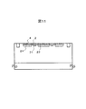
- FIG. 6 is an explanatory diagram of a process flow for manufacturing the element of Example 1;
- FIG. 6 is an explanatory diagram of a process flow for manufacturing the element of Example 1;
- FIG. 6 is an explanatory diagram of a process flow for manufacturing the element of Example 1;
- FIG. 6 is an explanatory diagram of a process flow for manufacturing the element of Example 1;
- 2 is an ion implantation profile into the bottom of a trench in Example 1.
- FIG. FIG. 6 is an explanatory diagram of a process flow for manufacturing the element of Example 1;
- FIG. 6 is an explanatory diagram of a process flow for manufacturing the element of Example 1;
- FIG. 6 is an explanatory diagram of a process flow for manufacturing the element of Example 1;
- FIG. 6 is an explanatory diagram of a process flow for manufacturing the element of Example 1;
- FIG. 6 is an explanatory diagram of a process flow for manufacturing the element of Example 1;
- FIG. 6 is an explanatory diagram of a process flow for manufacturing the element of Example 1;
- FIG. 6 is an explanatory diagram of a process flow for manufacturing the element of Example 1;
- FIG. 6 is an explanatory diagram of a process flow for manufacturing the element of Example 1;
- Example 1 a cross-sectional view of a trench type SiC-MOSFET unit cell is shown in FIG. This is a type of vertical MOS structure in which the current 21 flowing from the drain electrode 3 toward the source electrode 8 is controlled by the voltage applied to the gate electrode 6.
- a gate electrode is formed in the trench 12, and the channel 30 is along the side of the trench.
- An n drift layer (epi layer) 10 having a thickness and an impurity (impurity: nitrogen) concentration corresponding to a required breakdown voltage is formed on a SiC substrate 5 made of an n + layer (impurity: nitrogen) having a high impurity concentration and a low resistance of 20 m ⁇ cm.
- P body layer 7 impurity: aluminum
- source diffusion layer n + layer 2 impurity: nitrogen
- p + layer 4 for contact with p body layer 7 (impurity: aluminum)
- gate An insulating film 1 and a gate electrode 6 are formed.
- the n + layer 2 and the p + layer 4 are in ohmic contact with the source electrode 8 through the silicide layer 13.
- the depth of the p body layer 7 varies between the vicinity of the trench and between the trenches in order to increase the breakdown voltage, and the deep p body layer 24 is disposed between the trenches.
- n + layer (impurity: phosphorus) 31 having a higher concentration than the surroundings is in contact with the bottom of the trench.
- the thickness and concentration of the epi layer are determined according to the design breakdown voltage of the element. In the trench-type SiC-MOSFET having a withstand voltage of 600 V according to the present embodiment, the thickness of the epi layer is 8 ⁇ m and the impurity concentration is 2 ⁇ 10 16 cm ⁇ 3 .
- the (0001) plane (Si plane) of the 4H—SiC substrate is used as the main surface of the SiC substrate.
- FIG. 5 shows a blocking state in the trench type SiC-MOSFET structure of the first embodiment.
- a high voltage of 600 V is applied to the drain electrode 3 with respect to the source electrode 8 of 0 V.
- the gate electrode 6 is turned off at 0V.
- the potential difference of 600 V is blocked by the pn junction 32 in the reverse bias state, and the n ⁇ epilayer 10 whose concentration is low and the depletion layer easily spreads is responsible for most of it.
- FIG. 6 shows an electric field vector distribution in an enlarged region near the trench surrounded by 33 in FIG. In FIG.
- the electric field vector is concentrated toward the trench bottom 11 protruding into the n ⁇ layer, resulting in a high electric field.
- the electric field of the trench bottom silicon oxide film is relieved by the effect of the electric field vector extending toward the outside of the trench by the arrangement of the deep p body layer 24 and the effect of the thick silicon oxide film 34 at the trench bottom.
- the silicon oxide film Compared with SiC, the silicon oxide film has an electric field strength in the silicon oxide film of about 2 due to the difference in dielectric constant between SiC (dielectric constant 9.7) and silicon oxide film (SiO 2 , dielectric constant about 4). Increases 4 times.
- the thickness of the silicon oxide film at the bottom of the trench is set to a trench type so that the increase ratio of the electric field is offset by about 2.4 times so that the silicon oxide film at the bottom of the trench with a high electric field strength does not become a weak point for reliability. Reliability is ensured by a structure in which the thickness of the silicon oxide film, which is a uniform film in the Si-MOSFET, is three times or more.
- the maximum electric field strength in the silicon oxide film is reduced to 3 MV / cm or less by setting the thickness of the silicon oxide film on the side surface of the trench (channel portion) to 50 nm and the thickness of the silicon oxide film on the bottom of the trench to 200 nm. Suppressed.
- the breakdown voltage reliability can be improved without affecting the channel characteristics of the MOSFET.
- the accumulation n + layer 31 shown in FIG. 5 is formed in addition to the thickening of the trench bottom silicon oxide film. This accumulation n + layer 31 reduces the on-resistance.
- the silicon oxide film of this embodiment is not deposited by CVD or the like, but is formed by oxidizing SiC on the inner surface of the trench, impurities in each layer adjacent to the trench are included.
- the silicon oxide film at the bottom of the trench in contact with the accumulation n + layer 31 contains both phosphorus used as an impurity of the accumulation n + layer 31 and nitrogen used as an impurity of the n drift layer 10.
- the silicon oxide film in contact with the n drift layer 10 on the side surface of the trench contains nitrogen used as an impurity of the n drift layer 10, but may contain phosphorus used as an impurity of the accumulation n + layer 31 due to the range. However, since it is not intentionally included, it is extremely small or substantially absent.
- FIGS. 17 to 22 show cross-sectional views of the SiC substrate.
- An n + SiC substrate 5 having a 3 inch size on which an n drift layer 10 is epitaxially grown is prepared.
- FIG. 7 is a stage in which a trench 40 for alignment mark of photolithography having a depth of 1.5 ⁇ m is first formed on the SiC substrate by using photolithography and dry etching. Next, various ion implantation processes are performed. Each ion implantation step is performed by forming a hard mask 41 (SiO 2 film) by CVD, applying a photoresist 42, photolithography, development, dry etching of the hard mask (FIG.
- a hard mask 41 SiO 2 film
- the formation of the through film SiO 2 , the ion implantation 43 (FIG. 9), and the hard mask removal (FIG. 10) are taken as one set, and this is repeated for each process having different implantation patterns.
- the ion implantation process includes a shallow p body layer 23, a deep p body layer 24, a p + layer 4, a source n + layer 2, an accumulation n + layer 31 near the trench bottom, and a pattern of a termination portion around the chip (not shown) shown in FIG. Do each.
- ion implantation of an n + layer for forming an ohmic contact is performed on the back surface. Since the back surface is entirely implanted, no mask formation process is required.
- activation annealing for electrically activating the implanted impurities is performed at 1700 ° C. for 1 minute.
- heat treatment is performed in a state where carbon protective films are formed on the front and back surfaces.
- a silicon oxide film for hard mask having a thickness of 1 ⁇ m is formed on the surface by the CVD method, and a state shown in FIG. 12 is obtained through a photolithography process for forming a trench.
- the trench 12 is formed in SiC by dry etching using the hard mask 41, resulting in the state shown in FIG.
- the trench 12 is formed in a substantially vertical shape having a width of 0.5 ⁇ m, a depth of 0.6 ⁇ m, and a side surface angle of 85 degrees or more.
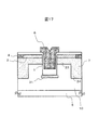
- FIG. 14 shows a process flow in which the vicinity of the trench is enlarged.
- the ion implantation species is phosphorus, and the energy and dose conditions are determined depending on the depth of the trench and the thickness of the bottom silicon oxide film to be formed later.
- the trench depth is 0.6 ⁇ m and the thickness of the bottom silicon oxide film is 200 nm
- the implantation profile has an impurity concentration of 2.0 ⁇ 10 20 to 2.6 ⁇ 10 20 cm ⁇ 3 in a region having a depth of 30 to 110 nm. Is done. That is, phosphorus is injected so that the box profile is 2.0 ⁇ 10 20 cm ⁇ 3 or more.
- a silicon oxide film of 20 nm is formed on the side surface of the trench and 100 nm on the bottom of the trench.
- the thickness of the silicon oxide film at the bottom of the trench is formed to be thicker than that of the side surface by generating a speed-up oxidation effect about five times by the ion implantation of the added phosphorus, so that the silicon oxide film can be formed at high speed.
- This ion implantation is due to the fact that lattice damage remains after the activation annealing process and the post-implantation heat treatment is not performed.
- CVD silicon oxide film formation (45 nm) are performed as a gate oxide film formation step, a total gate oxide film of 50 nm is formed on the side surface of the trench.
- the A silicon oxide film having a total thickness of 200 nm is formed at the bottom of the trench.
- This process is a process of changing the order of CVD silicon oxide film formation and annealing in a NO atmosphere to form a 45 nm CVD silicon oxide film and then heating it in a NO atmosphere at 1300 ° C. for 30 minutes. It may be replaced.
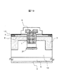
- a phosphorus-doped polysilicon film to be a gate electrode is formed inside the 300 nm trench and the gate electrode is patterned by photolithography, the state shown in FIG. 17 is obtained.
- the depth of the trench is minimized so that the gate length required from the design characteristics of the MOSFET can be secured and can be projected from the shallow p body layer 23.
- the maximum is determined so that the breakdown voltage does not deteriorate through the lower end of the deep p body layer 24.
- the dose amount of ions implanted with the profile shown in FIG. 15 is set so as to provide a speed-up oxidation effect at the bottom of the trench, and the depth is 200 nm of the thickness of the silicon oxide film formed in the oxidation process. Inject with the energy corresponding to (described above).
- an interlayer SiO 2 film of 300 nm is formed by CVD, a TiN film of 15 nm is formed by sputtering for preventing reaction in a later silicide process, and an opening pattern for a source contact is formed by photolithography. To do.
- the TiN film and the SiO 2 film are processed by dry etching to form an opening, the state shown in FIG. 18 is obtained.
- a Ni film 30 nm and a Ti film 15 nm for silicide formation are successively formed by sputtering, and a primary annealing for silicide is performed at 700 ° C. for 2 minutes, so that only the source contact portion where the SiC surface is exposed is selectively selected.
- a nickel silicide layer 13 is formed.
- the metal film remaining without the silicide reaction is removed with a cleaning chemical solution of sulfuric acid / hydrogen peroxide solution.
- a Ni film of 100 nm and a Ti film of 25 nm are deposited on the entire back surface to form ohmic contact silicide.
- FIG. 19 shows a stage in which heat treatment at 1000 ° C. for 2 minutes is performed as silicide annealing on both the front surface and the back surface, and the unreacted metal film is removed.
- an opening pattern for contact with the gate is formed by photolithography, and the SiO 2 film is opened by dry etching.
- a Ti film 10 nm, a TiN film 30 nm, and an aluminum film 5 ⁇ m are formed by sputtering, a metal wiring pattern is formed by photolithography, and the metal film is processed by dry etching. It is. Thereafter, a SiO 2 film is formed as a protective film, and an opening for the contact pad is formed using photolithography and wet etching.
- a photosensitive PIQ is applied as an organic protective film and an opening is formed by photolithography, the state shown in FIG. 21 is obtained.
- incidental processes such as a cleaning process, temporary protective film formation and removal, and an inspection process are appropriately included between the processes.
Landscapes
- Electrodes Of Semiconductors (AREA)
Abstract
トレンチ型SiC-MOSFETにおいて、トレンチ底部のゲート酸化膜の厚膜化を簡単に高速に行い効率よく製造できるようにするために、窒素がイオン注入されているドリフト層のトレンチ底部に位置する領域に対して酸化速度が速いリンを注入しておく。
Description
本発明は、炭化珪素半導体装置及びその製造方法に関する。
炭化珪素半導体装置のタイプの一つであるトレンチ型MOSFET構造の欠点は、トレンチが裏面のドレインに近いため、耐圧が低下しやすいことにある。図3にオフ状態の説明図を示す。高電圧がかかった状態(ブロッキング)では、主にドリフト層10中の空乏層が高電界を緩和している。トレンチ型MOSFETではトレンチ底部11がp型半導体領域のpボディ層7からドリフト層10中に突き出ているために、図3の26に示す電界ベクトルの集中が発生して破壊につながりやすい。特に、トレンチ底部11では、ゲート絶縁膜1を構成するシリコン酸化膜は誘電率が約4と4H-SiCの9.7に比べて低く、誘電率の比に従って電界強度はSiC中の2.4倍となり、電界が集中するトレンチ底部のゲート絶縁膜がウィークポイントとなる。
特許文献1では、トレンチ底部に窒素イオンを選択的に注入することでSiCをアモルファス化し、トレンチ底部が増速酸化されるようにしている。その結果、トレンチ側面よりも厚い酸化膜がトレンチ底部にできる。具体的な注入条件は、最大380KeVの注入エネルギーを持つ窒素イオンを1020cm-3の濃度で、深さ0.5μmのボックスプロファイルとなるようにウェハに対して垂直に注入している。
確かに、特許文献1のように、イオンを注入してアモルファス化すれば酸化速度は向上する。
しかし、窒素のイオン注入では酸化速度が十分ではない。
本発明の目的は、効率よく製造可能な高耐圧なトレンチ型SiC-MOSFETを提供することにある。
本発明は、上記課題を解決する発明を複数備える。そして、その代表的なものとしては、トレンチ構造のSiC-MOSFETを製造する際に、トレンチ形成工程の後で、SiCを酸化してゲート酸化膜を形成する酸化工程前に、トレンチ底面にリンを注入しておく。
本発明によれば、効率よく製造可能な高耐圧なトレンチ型SiC-MOSFETを製造できる。
以下、実施例を説明する。
実施例1として、トレンチ型SiC-MOSFETの単位セルの断面図を図1に示す。ドレイン電極3からソース電極8に向けて流れる電流21を、ゲート電極6に与える電圧で制御する縦型MOS構造の一種である。
ゲート電極をトレンチ12内に形成し、チャネル30はトレンチ側面に沿っている。不純物濃度が高く、20mΩcmと低抵抗なn+層(不純物:窒素)からなるSiC基板5上に、必要な耐圧に応じた厚みと不純物(不純物:窒素)濃度を持つnドリフト層(エピ層)10があり、さらに表面側にpボディ層7(不純物:アルミニウム)と、ソース拡散層のn+層2(不純物:窒素)、pボディ層7へのコンタクト用のp+層4(不純物:アルミニウム)、ゲート絶縁膜1、ゲート電極6が形成されている。n+層2とp+層4へはシリサイド層13を介してソース電極8へのオーミックコンタクトがとられている。
pボディ層7は、耐圧を高めるためにトレンチ近傍とトレンチ間でその深さが変わっており、トレンチ間には深いpボディ層24が配置されている。
また、トレンチ底部には周囲よりも高濃度なアキュムレーションn+層(不純物:リン)31が接している。エピ層の厚みと濃度は素子の設計耐圧に応じて決定する。本実施形態の600V耐圧のトレンチ型SiC-MOSFETにおいては、エピ層の厚さは8μm、不純物濃度は2×1016cm-3となる。SiC基板の主面には4H-SiC基板の(0001)面(Si面)を用いる。
従来技術のトレンチ型SiC-MOSFET構造のブロッキング状態は図3で示した。同様に、実施例1のトレンチ型SiC-MOSFET構造でのブロッキング状態を図5に示す。0Vのソース電極8に対して、ドレイン電極3に高電圧の600Vがかかる。ゲート電極6は0Vでオフをさせている。このとき電位差600Vは逆バイアス状態のpn接合32でブロックするが、特に濃度が低く空乏層が広がりやすいn-のエピ層10がその殆どを受け持つ。図5の33で囲んだトレンチ近傍を拡大した領域の電界ベクトル分布を図6に示す。従来技術の図3ではn-層中に突き出ているトレンチ底部11に向かって電界ベクトルが集中し高電界となっていたものが、図5と図6に示すように、本実施例の構造では、深いpボディ層24の配置で電界ベクトルの向きがトレンチ外側へ広がる効果と、トレンチ底部の厚いシリコン酸化膜34による効果とでトレンチ底部シリコン酸化膜の電界が緩和される。
SiCと比較してシリコン酸化膜ではSiC(誘電率9.7)とシリコン酸化膜(SiO2、誘電率約4)の誘電率差に起因して、シリコン酸化膜中の電界強度が約2.4倍に増加する。電界強度の高いトレンチ底部のシリコン酸化膜中が信頼性上のウィークポイントとならないように、電界の増加比約2.4倍を相殺するようにトレンチ底部のシリコン酸化膜の膜厚を、トレンチ型Si-MOSFETで均一膜としていたシリコン酸化膜の膜厚の3倍以上とする構造で信頼性を確保している。ここでは、トレンチ側面(チャネル部)のシリコン酸化膜の膜厚を50nmとし、トレンチ底部のシリコン酸化膜の膜厚を200nmとすることで、シリコン酸化膜中の最大電界強度を3MV/cm以下に抑制している。このように、チャネルとなるトレンチ側面のシリコン酸化膜の厚さは変えずに、トレンチ底部のみを厚膜化することで、MOSFETのチャネル特性に影響を与えずに耐圧信頼性を向上できる。
本実施例では、さらにオン抵抗の低減効果を得るために、トレンチ底部シリコン酸化膜の厚膜化に加えて、図5に示すアキュムレーションn+層31を形成した構成としている。このアキュムレーションn+層31によってオン抵抗を低減している。
本実施例のシリコン酸化膜は、CVDなどで堆積するものではなく、トレンチ内面のSiCを酸化して形成するので、トレンチに隣接する各層の不純物が含まれている。アキュムレーションn+層31に接するトレンチ底部のシリコン酸化膜にはアキュムレーションn+層31の不純物として使用したリンと、nドリフト層10の不純物として使用した窒素の両方が含まれている。トレンチ側面でnドリフト層10に接するシリコン酸化膜には、nドリフト層10の不純物として使用した窒素は含まれるが、アキュムレーションn+層31の不純物として使用したリンが飛程の影響で含まれる可能性はあるが意図的には含めないため、極めて少ないか、実質上含まれていないものである。
次に、本構造の素子を製造するためのプロセスフローを説明する。
図7~図15、図17~図22は、SiC基板の断面図を表している。nドリフト層10がエピタキシャル成長された3インチサイズのn+のSiC基板5を準備する。図7は、最初にホトリソグラフィとドライエッチングを用いて深さ1.5μmのホトリソグラフィのアライメントマーク用の溝40をSiC基板に形成した段階である。次に、各種のイオン注入工程を行う。各イオン注入工程は、CVD法によるハードマスク41(SiO2膜)の成膜、ホトレジスト42の塗布、ホトリソグラフィ、現像、ハードマスクのドライエッチング(図8)、アッシングによるホトレジスト除去、(必要に応じ)スルー膜SiO2の成膜、イオン注入43(図9)、ハードマスク除去(図10)、を1セットとして、注入パタンの異なる工程毎にこれを繰り返す。イオン注入工程は、図11に示す浅いpボディ層23、深いpボディ層24、p+層4、ソースn+層2、トレンチボトム付近のアキュムレーションn+層31、図示しないがチップ周辺のターミネーション部のパタンについて各々行う。基板表面のイオン注入後、裏面にオーミックコンタクト形成用のn+層のイオン注入を行う。裏面は全面注入のためマスク形成工程は不要である。
上記のイオン注入工程が一通り完了した後(図11)に、注入した不純物を電気的に活性化するための活性化アニールを1700℃、1分間行う。このとき、高温によるSiC基板表面からのSi脱離を防止する目的で、表裏面にカーボン保護膜を成膜した状態で熱処理する。保護膜の除去後、表面に厚さ1μmのハードマスク用シリコン酸化膜をCVD法で形成し、トレンチを形成するためのホトリソグラフィ工程を経ると図12の状態になる。ホトレジスト42をマスクにSiO2のハードマスク41をドライエッチングでパターニングし、ホトレジスト42をアッシングで除去した後に、ハードマスク41を用いてSiCにドライエッチングでトレンチ12を形成すると図13の状態になる。トレンチ12は幅0.5μm、深さ0.6μmで、側面角度は85度以上のほぼ垂直形状に形成する。
次に、トレンチ12の底部のみシリコン酸化膜の厚さを増加するため、本発明の特徴的な追加工程であるイオン注入工程を行う。トレンチ近傍を拡大したプロセスフローを図14に示す。トレンチ形成のハードマスク41を残してそのままイオン注入のマスクとしても用いることで、合わせずれなくトレンチ底部のみにイオン注入44が可能となり、余分な工程の増加を抑えることができる。
イオン注入種はリンで、エネルギーとドーズの条件は、トレンチの深さと、この後に形成される底部シリコン酸化膜の厚さに依存して決定する。ここではトレンチ深さ0.6μmで底部シリコン酸化膜の厚さを200nm形成する場合、(1)30keV、8×1014cm-2、(2)60keV、1.3×1015cm-2(3)100keV、1.7×1015cm-2(4)140keV、2×1015cm-2の条件で、順次チルト0°で垂直に注入する。このとき、注入プロファイルは図15に示すように深さ30~110nmの領域で不純物濃度が2.0×10²⁰~2.6×1020cm-3となり、図14の35に示す部分に注入される。すなわち、2.0×1020cm-3以上のボックスプロファイルとなるようにリンを注入する。
イオン注入後、1150℃、75分の犠牲酸化(ウェット酸化)を行うと、トレンチ側面部には20nm、トレンチ底部には100nmのシリコン酸化膜が形成される。トレンチ底部のシリコン酸化膜の厚さは、追加したリンのイオン注入により約5倍の増速酸化効果を生じて側面よりも厚く形成されるので、高速にシリコン酸化膜を形成できる。このイオン注入は活性化アニール工程後で、注入後の熱処理を行っておらず格子ダメージが残留していることに起因するが、注入種により速度が異なり、窒素を注入した場合よりもリンの方が極めて高速である。次いで、トレンチ側面に形成されたシリコン酸化膜の厚さ分を除去するだけのフッ酸洗浄を行い、側面のドライエッチダメージを除去する。ダメージ除去を確実にするために、この犠牲酸化工程(1150℃、75分)をもう一度繰り返し、再度シリコン酸化膜の除去を行う。この段階で、図16の36に示すようにトレンチ底部のみにシリコン酸化膜約150nmが残った状態となり、チャネルを形成するトレンチ側面には清浄な表面が露出する。ここで、ゲート酸化膜形成工程として、1300℃、5分のNO酸化(5nm相当)と、CVDシリコン酸化膜の成膜(45nm)を行うと、計50nmのゲート酸化膜がトレンチ側面に形成される。トレンチ底部には合計200nmのシリコン酸化膜が形成されている。なお、この工程は、CVDシリコン酸化膜の成膜とNO雰囲気でのアニールの順序を変えて、45nmのCVDシリコン酸化膜を成膜した後に、1300℃、30分、NO雰囲気で加熱する工程に代えてもよい。次いでゲート電極となるリンドープしたポリシリコン膜を300nmトレンチ内部に成膜し、ホトリソグラフィによりゲート電極のパターニングを行うと図17の状態となる。
トレンチの深さは、MOSFETの設計特性から必要なゲート長を確保した上で、浅いpボディ層23から突き出せるだけの寸法を最小限とする。最大限は、深いpボディ層24の下端を突き抜けて耐圧が劣化することが無いように決定する。このトレンチに対して、図15に示すプロファイルで注入したイオンのドーズ量はトレンチ底部に増速酸化効果をもたらすように設定し、その深さは酸化工程で形成されるシリコン酸化膜の厚さ200nmに対応するエネルギー(前述)で注入する。
続いて、CVD法で層間のSiO2膜300nmを成膜し、後のシリサイド工程での反応防止用にTiN膜15nmをスパッタで成膜し、ソースコンタクト用の開孔部パタンをホトリソグラフィで形成する。ドライエッチングによりTiN膜とSiO2膜を加工して開孔部を形成すると図18の状態となる。
シリサイド形成用のNi膜30nmとTi膜15nmを続けてスパッタで成膜し、シリサイド用の1次アニールを700℃、2分行って、SiC表面が露出しているソースコンタクト部のみに選択的にニッケルシリサイド層13を形成する。シリサイド反応をせずに残った金属膜は硫酸/過酸化水素水の洗浄薬液で除去する。続いて、裏面全面にもオーミックコンタクトのシリサイド形成用にNi膜100nmとTi膜25nmを堆積する。表面と裏面、両方のシリサイドアニールとして1000℃、2分の熱処理を行い、未反応のメタル膜を除去した段階が図19である。
続いて、ゲートへのコンタクト用開孔パタンをホトリソグラフィで形成し、ドライエッチングでSiO2膜を開孔する。ゲートとソースへのメタル配線として、Ti膜10nm、TiN膜30nm、アルミ膜5μmをスパッタで成膜し、メタル配線パタンをホトリソグラフィで形成し、ドライエッチングで上記メタル膜を加工した段階が図20である。その後、保護膜としてのSiO2膜を成膜し、コンタクトパッド用の開孔部をホトリソグラフィとウェットエッチングを用いて形成する。最後に、有機保護膜として感光性のPIQを塗布し、ホトリソグラフィによって開孔部を形成すると図21の状態になる。
記載を省略したが、各工程の間には適宜、洗浄工程や一時的な保護膜の成膜と除去、検査工程等の付帯的工程が含まれる。
1…ゲート絶縁膜、
2…ソース拡散層(n+)、
3…ドレイン電極、
4…コンタクト用のp+層、
5…SiC基板、
6…ゲート電極、
7…pボディ層、
8…ソース電極、
10…ドリフト層(エピ層)、
11…トレンチ底部、
12…トレンチ、
13…シリサイド層、
21…ソース電極に向けて流れる電流、
22…チャネルを流れる電流、
23…浅いpボディ層、
24…深いpボディ層、
25…深いpボディ層とトレンチとの距離、
26…電界ベクトル、
30…チャネル、
31…アキュムレーションn+層、
32…pn接合、
33…トレンチ近傍領域、
34…トレンチ底部の厚いシリコン酸化膜、
35…トレンチ底への追加のイオン注入部、
36…トレンチ底部のシリコン酸化膜、
40…アライメントマーク用の溝、
41…ハードマスク、
42…ホトレジスト、
43…SiC基板表面へのイオン注入、
44…トレンチ底部へのイオン注入、
45…TiN膜、
46…保護用のSiO2膜、
47…有機保護膜のPIQ
2…ソース拡散層(n+)、
3…ドレイン電極、
4…コンタクト用のp+層、
5…SiC基板、
6…ゲート電極、
7…pボディ層、
8…ソース電極、
10…ドリフト層(エピ層)、
11…トレンチ底部、
12…トレンチ、
13…シリサイド層、
21…ソース電極に向けて流れる電流、
22…チャネルを流れる電流、
23…浅いpボディ層、
24…深いpボディ層、
25…深いpボディ層とトレンチとの距離、
26…電界ベクトル、
30…チャネル、
31…アキュムレーションn+層、
32…pn接合、
33…トレンチ近傍領域、
34…トレンチ底部の厚いシリコン酸化膜、
35…トレンチ底への追加のイオン注入部、
36…トレンチ底部のシリコン酸化膜、
40…アライメントマーク用の溝、
41…ハードマスク、
42…ホトレジスト、
43…SiC基板表面へのイオン注入、
44…トレンチ底部へのイオン注入、
45…TiN膜、
46…保護用のSiO2膜、
47…有機保護膜のPIQ
Claims (7)
- 炭化珪素からなる基板が、前記基板主面上に形成された炭化珪素の第1導電型のドリフト層を備え、
前記エピタキシャル層表面に第1導電型のソース領域を有し、
前記エピタキシャル層中には、
第2導電型の第1ボディ領域と、
前記ソース領域から前記第1ボディ領域を貫通して前記ドリフト層まで延伸するトレンチと、
前記トレンチに形成された絶縁膜と、
前記トレンチ内に配置され、前記絶縁膜を介して前記ボディ層と接するゲート電極とを有し、
前記トレンチ底部の絶縁膜の厚さが前記トレンチ側面の絶縁膜の厚さより厚く、
前記ドリフト層には窒素が含まれており、
前記絶縁膜には窒素とリンが含まれていることを特徴とする炭化珪素半導体装置。 - 請求項1において、
前記ドリフト層の前記トレンチ底面に接する領域には窒素とリンを不純物として含むアキュムレーション領域を有することを特徴とする炭化珪素半導体装置。 - 請求項3において、
前記アキュムレーション領域には不純物原子が2×10²⁰/cm3以上注入されていることを特徴とする炭化珪素製半導体装置。 - 請求項1において、
前記第1ボディ領域より深く、前記トレンチから離れた位置に第2ボディ領域を有することを特徴とする炭化珪素半導体装置。 - 請求項2において、
前記トレンチ底部は、前記第2ボディ領域の底部よりも浅い位置に設けられることを特徴とする炭化珪素製半導体装置。 - 請求項1において、
前記アキュムレーション領域の不純物濃度は、前記ソース領域よりも低濃度で、かつ、前記ドリフト層よりも高濃度であることを特徴とする炭化珪素製半導体装置。 - 窒素を不純物として含むn型のドリフト層がエピタキシャル成長された炭化珪素からなるn型基板に対して、前記エピタキシャル層表面から不純物イオン注入して、n型のソース領域とp型のボディ領域とを形成し、活性化する工程と、
前記ソース領域から前記第1ボディ領域を貫通して前記ドリフト層まで延伸するトレンチを形成する工程と、
前記トレンチ底部のドリフト層に不純物としてリンを注入する工程と、
前記トレンチ内面を酸化する工程と、
前記トレンチ側面の酸化膜を除去する工程と、
前記トレンチ内面に酸化膜を堆積する工程とを有することを特徴とする炭化珪素半導体装置の製造方法。
Priority Applications (1)
| Application Number | Priority Date | Filing Date | Title |
|---|---|---|---|
| PCT/JP2012/084017 WO2014102994A1 (ja) | 2012-12-28 | 2012-12-28 | 炭化珪素半導体装置及びその製造方法 |
Applications Claiming Priority (1)
| Application Number | Priority Date | Filing Date | Title |
|---|---|---|---|
| PCT/JP2012/084017 WO2014102994A1 (ja) | 2012-12-28 | 2012-12-28 | 炭化珪素半導体装置及びその製造方法 |
Publications (1)
| Publication Number | Publication Date |
|---|---|
| WO2014102994A1 true WO2014102994A1 (ja) | 2014-07-03 |
Family
ID=51020145
Family Applications (1)
| Application Number | Title | Priority Date | Filing Date |
|---|---|---|---|
| PCT/JP2012/084017 Ceased WO2014102994A1 (ja) | 2012-12-28 | 2012-12-28 | 炭化珪素半導体装置及びその製造方法 |
Country Status (1)
| Country | Link |
|---|---|
| WO (1) | WO2014102994A1 (ja) |
Cited By (5)
| Publication number | Priority date | Publication date | Assignee | Title |
|---|---|---|---|---|
| WO2016067374A1 (ja) * | 2014-10-29 | 2016-05-06 | 株式会社日立製作所 | 半導体装置、パワーモジュール、および電力変換装置 |
| JP2017118024A (ja) * | 2015-12-25 | 2017-06-29 | 株式会社豊田中央研究所 | 炭化珪素半導体装置 |
| CN109698237A (zh) * | 2017-10-23 | 2019-04-30 | 株洲中车时代电气股份有限公司 | 一种沟槽栅碳化硅mosfet器件及其制造方法 |
| JP2020043197A (ja) * | 2018-09-10 | 2020-03-19 | 住友電気工業株式会社 | 炭化珪素半導体装置 |
| CN115513057A (zh) * | 2021-06-23 | 2022-12-23 | 上海艾为电子技术股份有限公司 | Mosfet及其制作方法 |
Citations (4)
| Publication number | Priority date | Publication date | Assignee | Title |
|---|---|---|---|---|
| JPH07240409A (ja) * | 1994-02-28 | 1995-09-12 | Fuji Electric Co Ltd | 炭化珪素半導体素子の製造方法 |
| JP2001077358A (ja) * | 1999-09-02 | 2001-03-23 | Fuji Electric Co Ltd | 炭化けい素umos半導体素子およびその製造方法 |
| JP2005005655A (ja) * | 2002-06-28 | 2005-01-06 | Internatl Rectifier Corp | Mosゲート半導体デバイス |
| JP2006228901A (ja) * | 2005-02-16 | 2006-08-31 | Fuji Electric Holdings Co Ltd | 炭化珪素半導体素子の製造方法 |
-
2012
- 2012-12-28 WO PCT/JP2012/084017 patent/WO2014102994A1/ja not_active Ceased
Patent Citations (4)
| Publication number | Priority date | Publication date | Assignee | Title |
|---|---|---|---|---|
| JPH07240409A (ja) * | 1994-02-28 | 1995-09-12 | Fuji Electric Co Ltd | 炭化珪素半導体素子の製造方法 |
| JP2001077358A (ja) * | 1999-09-02 | 2001-03-23 | Fuji Electric Co Ltd | 炭化けい素umos半導体素子およびその製造方法 |
| JP2005005655A (ja) * | 2002-06-28 | 2005-01-06 | Internatl Rectifier Corp | Mosゲート半導体デバイス |
| JP2006228901A (ja) * | 2005-02-16 | 2006-08-31 | Fuji Electric Holdings Co Ltd | 炭化珪素半導体素子の製造方法 |
Cited By (6)
| Publication number | Priority date | Publication date | Assignee | Title |
|---|---|---|---|---|
| WO2016067374A1 (ja) * | 2014-10-29 | 2016-05-06 | 株式会社日立製作所 | 半導体装置、パワーモジュール、および電力変換装置 |
| JP2017118024A (ja) * | 2015-12-25 | 2017-06-29 | 株式会社豊田中央研究所 | 炭化珪素半導体装置 |
| CN109698237A (zh) * | 2017-10-23 | 2019-04-30 | 株洲中车时代电气股份有限公司 | 一种沟槽栅碳化硅mosfet器件及其制造方法 |
| JP2020043197A (ja) * | 2018-09-10 | 2020-03-19 | 住友電気工業株式会社 | 炭化珪素半導体装置 |
| JP7056482B2 (ja) | 2018-09-10 | 2022-04-19 | 住友電気工業株式会社 | 炭化珪素半導体装置 |
| CN115513057A (zh) * | 2021-06-23 | 2022-12-23 | 上海艾为电子技术股份有限公司 | Mosfet及其制作方法 |
Similar Documents
| Publication | Publication Date | Title |
|---|---|---|
| JP4309967B2 (ja) | 半導体装置およびその製造方法 | |
| JP6099733B2 (ja) | 炭化珪素半導体装置 | |
| JP6707498B2 (ja) | シールドゲートを有する炭化珪素装置を形成する方法 | |
| CN101887854B (zh) | 碳化硅半导体装置及其制造方法 | |
| JP6119058B2 (ja) | 半導体装置 | |
| JP4435847B2 (ja) | 半導体装置およびその製造方法 | |
| US9252261B2 (en) | Semiconductor device and manufacturing method of the same | |
| CN102576723B (zh) | 半导体装置及其制造方法 | |
| CN103477439B (zh) | 半导体装置及其制造方法 | |
| US20160056266A1 (en) | Trench gate type semiconductor device and method of producing the same | |
| JP6766512B2 (ja) | 半導体装置および半導体装置の製造方法 | |
| JP5677330B2 (ja) | 炭化珪素半導体装置およびその製造方法 | |
| JP2011114028A (ja) | SiC半導体装置とその製造方法 | |
| US20110207275A1 (en) | Method for producing semiconductor element | |
| JP2018206872A (ja) | 半導体装置 | |
| WO2014102994A1 (ja) | 炭化珪素半導体装置及びその製造方法 | |
| JP2010182762A (ja) | 半導体素子及びこの製造方法 | |
| US9716159B1 (en) | Method of manufacturing silicon carbide semiconductor device | |
| JP5070935B2 (ja) | 炭化珪素半導体装置の製造方法 | |
| JP6024117B2 (ja) | 半導体装置の製造方法 | |
| JP2018110163A (ja) | 炭化珪素半導体装置および炭化珪素半導体装置の製造方法 | |
| KR101371491B1 (ko) | 반도체 소자 및 그 제조 방법 | |
| CN102738210A (zh) | 一种半导体装置及其制造方法 | |
| JP2013021219A (ja) | 半導体装置およびその製造方法 |
Legal Events
| Date | Code | Title | Description |
|---|---|---|---|
| 121 | Ep: the epo has been informed by wipo that ep was designated in this application |
Ref document number: 12891325 Country of ref document: EP Kind code of ref document: A1 |
|
| NENP | Non-entry into the national phase |
Ref country code: DE |
|
| 122 | Ep: pct application non-entry in european phase |
Ref document number: 12891325 Country of ref document: EP Kind code of ref document: A1 |
|
| NENP | Non-entry into the national phase |
Ref country code: JP |