WO2014103228A1 - Dispositif de dépôt chimique en phase vapeur assisté par plasma en ligne - Google Patents
Dispositif de dépôt chimique en phase vapeur assisté par plasma en ligne Download PDFInfo
- Publication number
- WO2014103228A1 WO2014103228A1 PCT/JP2013/007338 JP2013007338W WO2014103228A1 WO 2014103228 A1 WO2014103228 A1 WO 2014103228A1 JP 2013007338 W JP2013007338 W JP 2013007338W WO 2014103228 A1 WO2014103228 A1 WO 2014103228A1
- Authority
- WO
- WIPO (PCT)
- Prior art keywords
- chamber
- plasma cvd
- cvd apparatus
- substrate
- film
- Prior art date
- Legal status (The legal status is an assumption and is not a legal conclusion. Google has not performed a legal analysis and makes no representation as to the accuracy of the status listed.)
- Ceased
Links
Images










Classifications
-
- C—CHEMISTRY; METALLURGY
- C23—COATING METALLIC MATERIAL; COATING MATERIAL WITH METALLIC MATERIAL; CHEMICAL SURFACE TREATMENT; DIFFUSION TREATMENT OF METALLIC MATERIAL; COATING BY VACUUM EVAPORATION, BY SPUTTERING, BY ION IMPLANTATION OR BY CHEMICAL VAPOUR DEPOSITION, IN GENERAL; INHIBITING CORROSION OF METALLIC MATERIAL OR INCRUSTATION IN GENERAL
- C23C—COATING METALLIC MATERIAL; COATING MATERIAL WITH METALLIC MATERIAL; SURFACE TREATMENT OF METALLIC MATERIAL BY DIFFUSION INTO THE SURFACE, BY CHEMICAL CONVERSION OR SUBSTITUTION; COATING BY VACUUM EVAPORATION, BY SPUTTERING, BY ION IMPLANTATION OR BY CHEMICAL VAPOUR DEPOSITION, IN GENERAL
- C23C16/00—Chemical coating by decomposition of gaseous compounds, without leaving reaction products of surface material in the coating, i.e. chemical vapour deposition [CVD] processes
- C23C16/44—Chemical coating by decomposition of gaseous compounds, without leaving reaction products of surface material in the coating, i.e. chemical vapour deposition [CVD] processes characterised by the method of coating
- C23C16/54—Apparatus specially adapted for continuous coating
-
- C—CHEMISTRY; METALLURGY
- C23—COATING METALLIC MATERIAL; COATING MATERIAL WITH METALLIC MATERIAL; CHEMICAL SURFACE TREATMENT; DIFFUSION TREATMENT OF METALLIC MATERIAL; COATING BY VACUUM EVAPORATION, BY SPUTTERING, BY ION IMPLANTATION OR BY CHEMICAL VAPOUR DEPOSITION, IN GENERAL; INHIBITING CORROSION OF METALLIC MATERIAL OR INCRUSTATION IN GENERAL
- C23C—COATING METALLIC MATERIAL; COATING MATERIAL WITH METALLIC MATERIAL; SURFACE TREATMENT OF METALLIC MATERIAL BY DIFFUSION INTO THE SURFACE, BY CHEMICAL CONVERSION OR SUBSTITUTION; COATING BY VACUUM EVAPORATION, BY SPUTTERING, BY ION IMPLANTATION OR BY CHEMICAL VAPOUR DEPOSITION, IN GENERAL
- C23C16/00—Chemical coating by decomposition of gaseous compounds, without leaving reaction products of surface material in the coating, i.e. chemical vapour deposition [CVD] processes
- C23C16/22—Chemical coating by decomposition of gaseous compounds, without leaving reaction products of surface material in the coating, i.e. chemical vapour deposition [CVD] processes characterised by the deposition of inorganic material, other than metallic material
- C23C16/26—Deposition of carbon only
-
- C—CHEMISTRY; METALLURGY
- C23—COATING METALLIC MATERIAL; COATING MATERIAL WITH METALLIC MATERIAL; CHEMICAL SURFACE TREATMENT; DIFFUSION TREATMENT OF METALLIC MATERIAL; COATING BY VACUUM EVAPORATION, BY SPUTTERING, BY ION IMPLANTATION OR BY CHEMICAL VAPOUR DEPOSITION, IN GENERAL; INHIBITING CORROSION OF METALLIC MATERIAL OR INCRUSTATION IN GENERAL
- C23C—COATING METALLIC MATERIAL; COATING MATERIAL WITH METALLIC MATERIAL; SURFACE TREATMENT OF METALLIC MATERIAL BY DIFFUSION INTO THE SURFACE, BY CHEMICAL CONVERSION OR SUBSTITUTION; COATING BY VACUUM EVAPORATION, BY SPUTTERING, BY ION IMPLANTATION OR BY CHEMICAL VAPOUR DEPOSITION, IN GENERAL
- C23C16/00—Chemical coating by decomposition of gaseous compounds, without leaving reaction products of surface material in the coating, i.e. chemical vapour deposition [CVD] processes
- C23C16/44—Chemical coating by decomposition of gaseous compounds, without leaving reaction products of surface material in the coating, i.e. chemical vapour deposition [CVD] processes characterised by the method of coating
- C23C16/4401—Means for minimising impurities, e.g. dust, moisture or residual gas, in the reaction chamber
-
- C—CHEMISTRY; METALLURGY
- C23—COATING METALLIC MATERIAL; COATING MATERIAL WITH METALLIC MATERIAL; CHEMICAL SURFACE TREATMENT; DIFFUSION TREATMENT OF METALLIC MATERIAL; COATING BY VACUUM EVAPORATION, BY SPUTTERING, BY ION IMPLANTATION OR BY CHEMICAL VAPOUR DEPOSITION, IN GENERAL; INHIBITING CORROSION OF METALLIC MATERIAL OR INCRUSTATION IN GENERAL
- C23C—COATING METALLIC MATERIAL; COATING MATERIAL WITH METALLIC MATERIAL; SURFACE TREATMENT OF METALLIC MATERIAL BY DIFFUSION INTO THE SURFACE, BY CHEMICAL CONVERSION OR SUBSTITUTION; COATING BY VACUUM EVAPORATION, BY SPUTTERING, BY ION IMPLANTATION OR BY CHEMICAL VAPOUR DEPOSITION, IN GENERAL
- C23C16/00—Chemical coating by decomposition of gaseous compounds, without leaving reaction products of surface material in the coating, i.e. chemical vapour deposition [CVD] processes
- C23C16/44—Chemical coating by decomposition of gaseous compounds, without leaving reaction products of surface material in the coating, i.e. chemical vapour deposition [CVD] processes characterised by the method of coating
- C23C16/4401—Means for minimising impurities, e.g. dust, moisture or residual gas, in the reaction chamber
- C23C16/4409—Means for minimising impurities, e.g. dust, moisture or residual gas, in the reaction chamber characterised by sealing means
-
- C—CHEMISTRY; METALLURGY
- C23—COATING METALLIC MATERIAL; COATING MATERIAL WITH METALLIC MATERIAL; CHEMICAL SURFACE TREATMENT; DIFFUSION TREATMENT OF METALLIC MATERIAL; COATING BY VACUUM EVAPORATION, BY SPUTTERING, BY ION IMPLANTATION OR BY CHEMICAL VAPOUR DEPOSITION, IN GENERAL; INHIBITING CORROSION OF METALLIC MATERIAL OR INCRUSTATION IN GENERAL
- C23C—COATING METALLIC MATERIAL; COATING MATERIAL WITH METALLIC MATERIAL; SURFACE TREATMENT OF METALLIC MATERIAL BY DIFFUSION INTO THE SURFACE, BY CHEMICAL CONVERSION OR SUBSTITUTION; COATING BY VACUUM EVAPORATION, BY SPUTTERING, BY ION IMPLANTATION OR BY CHEMICAL VAPOUR DEPOSITION, IN GENERAL
- C23C16/00—Chemical coating by decomposition of gaseous compounds, without leaving reaction products of surface material in the coating, i.e. chemical vapour deposition [CVD] processes
- C23C16/44—Chemical coating by decomposition of gaseous compounds, without leaving reaction products of surface material in the coating, i.e. chemical vapour deposition [CVD] processes characterised by the method of coating
- C23C16/4412—Details relating to the exhausts, e.g. pumps, filters, scrubbers, particle traps
-
- C—CHEMISTRY; METALLURGY
- C23—COATING METALLIC MATERIAL; COATING MATERIAL WITH METALLIC MATERIAL; CHEMICAL SURFACE TREATMENT; DIFFUSION TREATMENT OF METALLIC MATERIAL; COATING BY VACUUM EVAPORATION, BY SPUTTERING, BY ION IMPLANTATION OR BY CHEMICAL VAPOUR DEPOSITION, IN GENERAL; INHIBITING CORROSION OF METALLIC MATERIAL OR INCRUSTATION IN GENERAL
- C23C—COATING METALLIC MATERIAL; COATING MATERIAL WITH METALLIC MATERIAL; SURFACE TREATMENT OF METALLIC MATERIAL BY DIFFUSION INTO THE SURFACE, BY CHEMICAL CONVERSION OR SUBSTITUTION; COATING BY VACUUM EVAPORATION, BY SPUTTERING, BY ION IMPLANTATION OR BY CHEMICAL VAPOUR DEPOSITION, IN GENERAL
- C23C16/00—Chemical coating by decomposition of gaseous compounds, without leaving reaction products of surface material in the coating, i.e. chemical vapour deposition [CVD] processes
- C23C16/44—Chemical coating by decomposition of gaseous compounds, without leaving reaction products of surface material in the coating, i.e. chemical vapour deposition [CVD] processes characterised by the method of coating
- C23C16/458—Chemical coating by decomposition of gaseous compounds, without leaving reaction products of surface material in the coating, i.e. chemical vapour deposition [CVD] processes characterised by the method of coating characterised by the method used for supporting substrates in the reaction chamber
- C23C16/4582—Rigid and flat substrates, e.g. plates or discs
- C23C16/4583—Rigid and flat substrates, e.g. plates or discs the substrate being supported substantially horizontally
- C23C16/4584—Rigid and flat substrates, e.g. plates or discs the substrate being supported substantially horizontally the substrate being rotated
-
- C—CHEMISTRY; METALLURGY
- C23—COATING METALLIC MATERIAL; COATING MATERIAL WITH METALLIC MATERIAL; CHEMICAL SURFACE TREATMENT; DIFFUSION TREATMENT OF METALLIC MATERIAL; COATING BY VACUUM EVAPORATION, BY SPUTTERING, BY ION IMPLANTATION OR BY CHEMICAL VAPOUR DEPOSITION, IN GENERAL; INHIBITING CORROSION OF METALLIC MATERIAL OR INCRUSTATION IN GENERAL
- C23C—COATING METALLIC MATERIAL; COATING MATERIAL WITH METALLIC MATERIAL; SURFACE TREATMENT OF METALLIC MATERIAL BY DIFFUSION INTO THE SURFACE, BY CHEMICAL CONVERSION OR SUBSTITUTION; COATING BY VACUUM EVAPORATION, BY SPUTTERING, BY ION IMPLANTATION OR BY CHEMICAL VAPOUR DEPOSITION, IN GENERAL
- C23C16/00—Chemical coating by decomposition of gaseous compounds, without leaving reaction products of surface material in the coating, i.e. chemical vapour deposition [CVD] processes
- C23C16/44—Chemical coating by decomposition of gaseous compounds, without leaving reaction products of surface material in the coating, i.e. chemical vapour deposition [CVD] processes characterised by the method of coating
- C23C16/458—Chemical coating by decomposition of gaseous compounds, without leaving reaction products of surface material in the coating, i.e. chemical vapour deposition [CVD] processes characterised by the method of coating characterised by the method used for supporting substrates in the reaction chamber
- C23C16/4582—Rigid and flat substrates, e.g. plates or discs
- C23C16/4587—Rigid and flat substrates, e.g. plates or discs the substrate being supported substantially vertically
- C23C16/4588—Rigid and flat substrates, e.g. plates or discs the substrate being supported substantially vertically the substrate being rotated
-
- C—CHEMISTRY; METALLURGY
- C23—COATING METALLIC MATERIAL; COATING MATERIAL WITH METALLIC MATERIAL; CHEMICAL SURFACE TREATMENT; DIFFUSION TREATMENT OF METALLIC MATERIAL; COATING BY VACUUM EVAPORATION, BY SPUTTERING, BY ION IMPLANTATION OR BY CHEMICAL VAPOUR DEPOSITION, IN GENERAL; INHIBITING CORROSION OF METALLIC MATERIAL OR INCRUSTATION IN GENERAL
- C23C—COATING METALLIC MATERIAL; COATING MATERIAL WITH METALLIC MATERIAL; SURFACE TREATMENT OF METALLIC MATERIAL BY DIFFUSION INTO THE SURFACE, BY CHEMICAL CONVERSION OR SUBSTITUTION; COATING BY VACUUM EVAPORATION, BY SPUTTERING, BY ION IMPLANTATION OR BY CHEMICAL VAPOUR DEPOSITION, IN GENERAL
- C23C16/00—Chemical coating by decomposition of gaseous compounds, without leaving reaction products of surface material in the coating, i.e. chemical vapour deposition [CVD] processes
- C23C16/44—Chemical coating by decomposition of gaseous compounds, without leaving reaction products of surface material in the coating, i.e. chemical vapour deposition [CVD] processes characterised by the method of coating
- C23C16/50—Chemical coating by decomposition of gaseous compounds, without leaving reaction products of surface material in the coating, i.e. chemical vapour deposition [CVD] processes characterised by the method of coating using electric discharges
- C23C16/503—Chemical coating by decomposition of gaseous compounds, without leaving reaction products of surface material in the coating, i.e. chemical vapour deposition [CVD] processes characterised by the method of coating using electric discharges using DC or AC discharges
-
- C—CHEMISTRY; METALLURGY
- C23—COATING METALLIC MATERIAL; COATING MATERIAL WITH METALLIC MATERIAL; CHEMICAL SURFACE TREATMENT; DIFFUSION TREATMENT OF METALLIC MATERIAL; COATING BY VACUUM EVAPORATION, BY SPUTTERING, BY ION IMPLANTATION OR BY CHEMICAL VAPOUR DEPOSITION, IN GENERAL; INHIBITING CORROSION OF METALLIC MATERIAL OR INCRUSTATION IN GENERAL
- C23C—COATING METALLIC MATERIAL; COATING MATERIAL WITH METALLIC MATERIAL; SURFACE TREATMENT OF METALLIC MATERIAL BY DIFFUSION INTO THE SURFACE, BY CHEMICAL CONVERSION OR SUBSTITUTION; COATING BY VACUUM EVAPORATION, BY SPUTTERING, BY ION IMPLANTATION OR BY CHEMICAL VAPOUR DEPOSITION, IN GENERAL
- C23C16/00—Chemical coating by decomposition of gaseous compounds, without leaving reaction products of surface material in the coating, i.e. chemical vapour deposition [CVD] processes
- C23C16/44—Chemical coating by decomposition of gaseous compounds, without leaving reaction products of surface material in the coating, i.e. chemical vapour deposition [CVD] processes characterised by the method of coating
- C23C16/50—Chemical coating by decomposition of gaseous compounds, without leaving reaction products of surface material in the coating, i.e. chemical vapour deposition [CVD] processes characterised by the method of coating using electric discharges
- C23C16/505—Chemical coating by decomposition of gaseous compounds, without leaving reaction products of surface material in the coating, i.e. chemical vapour deposition [CVD] processes characterised by the method of coating using electric discharges using radio frequency discharges
-
- H—ELECTRICITY
- H01—ELECTRIC ELEMENTS
- H01J—ELECTRIC DISCHARGE TUBES OR DISCHARGE LAMPS
- H01J37/00—Discharge tubes with provision for introducing objects or material to be exposed to the discharge, e.g. for the purpose of examination or processing thereof
- H01J37/32—Gas-filled discharge tubes
- H01J37/32431—Constructional details of the reactor
- H01J37/32532—Electrodes
- H01J37/32568—Relative arrangement or disposition of electrodes; moving means
-
- H—ELECTRICITY
- H01—ELECTRIC ELEMENTS
- H01J—ELECTRIC DISCHARGE TUBES OR DISCHARGE LAMPS
- H01J37/00—Discharge tubes with provision for introducing objects or material to be exposed to the discharge, e.g. for the purpose of examination or processing thereof
- H01J37/32—Gas-filled discharge tubes
- H01J37/32431—Constructional details of the reactor
- H01J37/32697—Electrostatic control
- H01J37/32706—Polarising the substrate
-
- H—ELECTRICITY
- H01—ELECTRIC ELEMENTS
- H01J—ELECTRIC DISCHARGE TUBES OR DISCHARGE LAMPS
- H01J37/00—Discharge tubes with provision for introducing objects or material to be exposed to the discharge, e.g. for the purpose of examination or processing thereof
- H01J37/32—Gas-filled discharge tubes
- H01J37/32431—Constructional details of the reactor
- H01J37/32715—Workpiece holder
-
- H—ELECTRICITY
- H01—ELECTRIC ELEMENTS
- H01J—ELECTRIC DISCHARGE TUBES OR DISCHARGE LAMPS
- H01J37/00—Discharge tubes with provision for introducing objects or material to be exposed to the discharge, e.g. for the purpose of examination or processing thereof
- H01J37/32—Gas-filled discharge tubes
- H01J37/32431—Constructional details of the reactor
- H01J37/32733—Means for moving the material to be treated
- H01J37/32752—Means for moving the material to be treated for moving the material across the discharge
- H01J37/32761—Continuous moving
- H01J37/32779—Continuous moving of batches of workpieces
-
- H—ELECTRICITY
- H01—ELECTRIC ELEMENTS
- H01J—ELECTRIC DISCHARGE TUBES OR DISCHARGE LAMPS
- H01J37/00—Discharge tubes with provision for introducing objects or material to be exposed to the discharge, e.g. for the purpose of examination or processing thereof
- H01J37/32—Gas-filled discharge tubes
- H01J37/32431—Constructional details of the reactor
- H01J37/32798—Further details of plasma apparatus not provided for in groups H01J37/3244 - H01J37/32788; special provisions for cleaning or maintenance of the apparatus
- H01J37/32853—Hygiene
-
- H—ELECTRICITY
- H01—ELECTRIC ELEMENTS
- H01J—ELECTRIC DISCHARGE TUBES OR DISCHARGE LAMPS
- H01J37/00—Discharge tubes with provision for introducing objects or material to be exposed to the discharge, e.g. for the purpose of examination or processing thereof
- H01J37/32—Gas-filled discharge tubes
- H01J37/32431—Constructional details of the reactor
- H01J37/32798—Further details of plasma apparatus not provided for in groups H01J37/3244 - H01J37/32788; special provisions for cleaning or maintenance of the apparatus
- H01J37/32899—Multiple chambers, e.g. cluster tools
-
- H—ELECTRICITY
- H10—SEMICONDUCTOR DEVICES; ELECTRIC SOLID-STATE DEVICES NOT OTHERWISE PROVIDED FOR
- H10P—GENERIC PROCESSES OR APPARATUS FOR THE MANUFACTURE OR TREATMENT OF DEVICES COVERED BY CLASS H10
- H10P72/00—Handling or holding of wafers, substrates or devices during manufacture or treatment thereof
- H10P72/04—Apparatus for manufacture or treatment
- H10P72/0451—Apparatus for manufacturing or treating in a plurality of work-stations
- H10P72/0452—Apparatus for manufacturing or treating in a plurality of work-stations characterised by the layout of the process chambers
- H10P72/0456—Apparatus for manufacturing or treating in a plurality of work-stations characterised by the layout of the process chambers in-line arrangement
-
- H—ELECTRICITY
- H10—SEMICONDUCTOR DEVICES; ELECTRIC SOLID-STATE DEVICES NOT OTHERWISE PROVIDED FOR
- H10P—GENERIC PROCESSES OR APPARATUS FOR THE MANUFACTURE OR TREATMENT OF DEVICES COVERED BY CLASS H10
- H10P72/00—Handling or holding of wafers, substrates or devices during manufacture or treatment thereof
- H10P72/04—Apparatus for manufacture or treatment
- H10P72/0451—Apparatus for manufacturing or treating in a plurality of work-stations
- H10P72/0466—Apparatus for manufacturing or treating in a plurality of work-stations characterised by the construction of the load-lock chamber
-
- H—ELECTRICITY
- H10—SEMICONDUCTOR DEVICES; ELECTRIC SOLID-STATE DEVICES NOT OTHERWISE PROVIDED FOR
- H10P—GENERIC PROCESSES OR APPARATUS FOR THE MANUFACTURE OR TREATMENT OF DEVICES COVERED BY CLASS H10
- H10P72/00—Handling or holding of wafers, substrates or devices during manufacture or treatment thereof
- H10P72/30—Handling or holding of wafers, substrates or devices during manufacture or treatment thereof for conveying, e.g. between different workstations
- H10P72/33—Handling or holding of wafers, substrates or devices during manufacture or treatment thereof for conveying, e.g. between different workstations into and out of processing chamber
- H10P72/3311—Horizontal transfer of a batch of workpieces
-
- H—ELECTRICITY
- H10—SEMICONDUCTOR DEVICES; ELECTRIC SOLID-STATE DEVICES NOT OTHERWISE PROVIDED FOR
- H10P—GENERIC PROCESSES OR APPARATUS FOR THE MANUFACTURE OR TREATMENT OF DEVICES COVERED BY CLASS H10
- H10P72/00—Handling or holding of wafers, substrates or devices during manufacture or treatment thereof
- H10P72/30—Handling or holding of wafers, substrates or devices during manufacture or treatment thereof for conveying, e.g. between different workstations
- H10P72/33—Handling or holding of wafers, substrates or devices during manufacture or treatment thereof for conveying, e.g. between different workstations into and out of processing chamber
- H10P72/3314—Continuous loading and unloading into and out of a processing chamber, e.g. transporting belts within processing chambers
Definitions
- the present invention relates to a plasma CVD apparatus for forming a CVD film on a substrate, and more particularly to an in-line plasma CVD apparatus with high production efficiency while maintaining stable film forming conditions.
- a so-called in-line type device or a device with a load lock chamber is employed.
- These apparatuses include a film formation chamber and a chamber dedicated to evacuation and the like provided separately, and a substrate is transported between the chambers. Thus, a number of film formation cycles are performed while the film formation chamber is always maintained in a vacuum state.
- Patent Document 1 discloses an improved technique for an in-line type plasma CVD apparatus that forms a film on the surface of an object to be processed (base material, substrate) by plasma CVD.
- FIG. 2 of Patent Document 1 discloses a typical example of an in-line type plasma CVD apparatus as a conventional technique. According to FIG. 2 and the description thereof, this in-line type plasma CVD apparatus includes a plurality of independent chambers (partition chambers) partitioned from each other, and in each chamber, evacuation / heating of the base material, film formation, Each step in the open film forming process is performed individually. The base material is sequentially conveyed inside the apparatus, whereby the film forming process is executed.
- each stage of the process is performed in a room independent from each other, so that high productivity can be expected, and it is not necessary to open the film forming chamber to the atmosphere each time a substrate is inserted. There is no gas adsorption in the room, and it can be expected that a high-quality film can be stably formed.
- an in-line plasma CVD apparatus is provided with an atmospheric heating furnace for preheating the base material under atmospheric pressure, and the temperature rise time until the base material is set to a predetermined temperature in the load chamber is set. A technique for shortening is disclosed.
- the film is not only formed on the substrate to be formed, but also deposited on the wall of the film forming chamber, the electrode facing the substrate, or the like.
- a film is likely to be formed at a place where a current for generating plasma is passed.
- the substrate to be deposited and the jig that supports it are removed when the deposition process is completed, and replaced with the object to be processed next, but the electrodes facing the walls of the deposition chamber and the substrate, etc. Is used over many treatments, so that a thick film is deposited as the deposition cycle is repeated.
- a high-frequency electrode denoted by reference numeral 30 in FIG. 2 of Patent Document 1 and a substrate mounted on a substrate cart denoted by reference numeral 1 are provided.
- high frequency power is applied to the high frequency electrode to generate plasma, thereby forming a film on the base material, and at the same time, the high frequency electrode has a film of the same amount as the film on the base material. Accumulates.
- the substrate cart and the substrate are replaced with new ones every time the film formation cycle is completed, but the coating is continuously deposited because the high-frequency electrode is always used.
- the film deposited and thick in this manner is easily peeled off and scattered, which can cause film defects. Such internal deposits need to be removed by regular cleaning.
- the film formed by the plasma CVD method is an insulating film such as DLC
- another problem occurs. That is, as the film formation proceeds and the film thickness increases, the insulating film generates a resistance component when power is supplied. For this reason, even if the same power condition is set, there arises a problem that the state of plasma generation varies and the characteristics of the film also change.
- the plasma CVD apparatus there is a method of applying electric power to the base material and the base material cart side with the high-frequency electrode portion being a simple chamber wall.
- a film is deposited on the chamber wall facing the substrate in the same manner as the substrate.
- the electric resistance of the inner wall of the chamber is increased because the film exists in a portion where electric power flows. Therefore, there is a possibility that the generation of plasma generated using the inner wall as one electrode becomes unstable, or that the operating conditions deviate from the optimum conditions.
- the present invention provides an in-line type plasma CVD apparatus, which is difficult to deposit a CVD film on a portion other than a base material, can be stably operated without cleaning over a long period of time, and has a high production efficiency.
- the purpose is to do.
- An in-line type plasma CVD apparatus includes a film formation chamber and a compartment different from the film formation chamber, and a substrate is transported between the film formation chamber and the compartment.
- the film forming chamber includes a vacuum chamber, a pump that exhausts air in the vacuum chamber, a gas supply unit that supplies a source gas into the vacuum chamber, and plasma is supplied to the source gas supplied into the vacuum chamber.
- An AC type plasma generating power source to be generated.
- the base material is divided into two groups, and any one of a first group connected to one electrode of the plasma generating power source and a second group connected to the other electrode of the plasma generating power source. Belongs to.
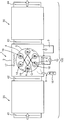
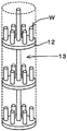
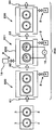
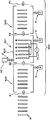
- FIG. 1 is a perspective view showing an overall configuration of an inline-type plasma CVD apparatus according to a first embodiment of the present invention. It is a top view of the in-line type plasma CVD apparatus shown in FIG. It is the perspective view which showed the example of installation of the base material to the autorotation table of the said plasma CVD apparatus. It is the perspective view which showed the example of installation of the base material to the autorotation table of the said plasma CVD apparatus. It is a top view for demonstrating the operation state of the in-line type plasma CVD apparatus shown in FIG. It is a side view for demonstrating the operation state of the in-line type plasma CVD apparatus shown in FIG.
- the in-line type has a load lock chamber (preliminary exhaust chamber), and the substrate is exchanged between the outside of the apparatus (atmospheric pressure) and the film forming chamber (vacuum pressure) through this chamber.
- This is a general term for the system of a device having a mechanism that keeps the film forming chamber in a vacuum state at all times including when the substrate is replaced, and also includes a load lock type, an inter-back type, and a multi-chamber type.
- the target of the film forming process in the plasma CVD apparatus 100 is the substrate W.
- FIG. 1 is a perspective view showing an overall configuration of a plasma CVD apparatus 100 according to the first embodiment of the present invention
- FIG. 2 is a top view thereof.
- the plasma CVD apparatus 100 includes a film formation chamber 1 having a plasma CVD mechanism, a load lock chamber 20 that is another compartment disposed on the upstream side of the film formation chamber 1, and a downstream side of the film formation chamber 1.
- a load lock chamber (compartment) 30 which is another compartment arranged. Here, upstream and downstream are in the direction of transport of the substrate W.
- a gate valve 41 is provided at the inlet of the load lock chamber 20, and a gate valve 42 is provided between the outlet of the load lock chamber 20 and the inlet of the film forming chamber 1, and the outlet of the film forming chamber 1 and the inlet of the load lock chamber 30.
- a gate valve 43 and a gate valve 44 at the outlet of the load lock chamber 30 are respectively installed between the two. 1 shows only the gate valve 44, the plasma CVD apparatus 100 is provided with four gate valves 41 to 44 (in other words, gates 41 to 44) as shown in FIG.
- the base material W is divided into two groups. At least in the film forming chamber 1, a vacuum chamber 2 described later is grounded, the two groups are insulated from the vacuum chamber 2, and the groups are also insulated from each other. Thus, each group can have an independent potential. Details of this will be described later.
- the load lock chamber 20 includes a gate valve 41 serving as a door for carrying the substrate W and a vacuum exhaust mechanism.
- the substrate W and the substrate table are carried into the load lock chamber 20 from the outside of the plasma CVD apparatus 100 with the gate valve 41 opened (the gate valve 42 is closed at this time) and opened to the atmosphere. Thereafter, when the gate valve 41 is closed (the gate valve 42 is kept closed at this time), the inside of the load lock chamber 20 can be evacuated to a vacuum.
- the gate valve 42 between the film formation chamber 1 and the vacuum chamber is previously opened (the gate valve 41 at this time).
- 43 is in a closed state), and the substrate W and the substrate table are transferred to the film forming chamber 1 in a vacuum state.
- the plasma CVD apparatus 100 includes a transfer mechanism for transferring the substrate W and the substrate table between the chambers.
- the gate valve 42 is closed, the atmosphere is introduced into the load lock chamber 20, and the load lock chamber 20 is brought to atmospheric pressure. As a result, the base material W and the base material table of the next lot can be received.
- the film forming chamber 1 includes a vacuum chamber 2, a vacuum pump 3 that is a vacuum exhaust means for evacuating the inside of the vacuum chamber 2, and a vacuum that is evacuated by the vacuum pump 3.
- a gas supply unit 9 for supplying a source gas into the chamber 2 and an AC power supply type plasma generation power source 10 for generating plasma in the process gas supplied into the vacuum chamber 2 are provided.
- the two groups of base materials W are connected to both electrodes of the plasma generation power source 10, and glow discharge is generated by the voltage applied between the two groups of base materials W to form a film.
- a downstream load lock chamber 30 is connected to the film forming chamber 1 via a gate valve 43.
- the load lock chamber 30 includes a gate valve 44 serving as a door for carrying out the substrate W and a vacuum exhaust mechanism.
- a gate valve 44 serving as a door for carrying out the substrate W and a vacuum exhaust mechanism.
- the plasma CVD apparatus 100 includes a transfer mechanism for transferring the substrate W and the substrate table between the chambers.
- the gate valve 44 is closed and the interior of the load lock chamber 30 is evacuated to a vacuum.
- the load lock chamber 30 is ready to receive the lot of the substrate W and the substrate table from the film forming chamber 1.
- the above-described configuration of the plasma CVD apparatus 100 according to the first embodiment is a normal so-called in-line type, except that AC power is applied to the base material W divided into two groups, which is a feature of the present invention described later.
- This is the same as the film forming apparatus. Therefore, the plasma CVD apparatus 100 has a general advantage of the in-line type film forming apparatus, that is, the film forming chamber is less likely to be exposed to the atmosphere and can be stably covered, and can be processed with a short tact time. It has advantages such as mass production.
- the plasma CVD apparatus 100 has a disadvantage of a normal in-line film forming apparatus, that is, a load lock chamber 20 for cleaning a film deposited on the inner wall surface of the film forming chamber 1 that is less exposed to the atmosphere.
- the film forming chamber 1 sandwiched between the load lock chambers 30 has the disadvantage of having to be open to the atmosphere by contriving the structure of the film forming chamber 1.
- the configuration of the film forming chamber 1 of the plasma CVD apparatus 100 will be described in detail.
- the configuration of the film forming chamber 1 in the plasma CVD apparatus 100 will be described with reference to FIGS. 1 to 4B.
- the vacuum chamber 2 is a casing whose inside can be hermetically sealed from the outside.
- the vacuum pump 3 is provided on the side of the vacuum chamber 2 and exhausts the gas in the vacuum chamber 2 to the outside to bring the inside of the vacuum chamber 2 into a low pressure state.
- the vacuum pump 3 can reduce the pressure in the vacuum chamber 2 to a vacuum state.
- the plasma CVD apparatus 100 further includes a substrate table.
- a plurality of substrates W can be mounted on the substrate table, and the substrate W can be processed inside the vacuum chamber 2 in the mounted state.
- the base material table has a mechanism for causing the base material W mounted on the base material table to undergo planetary rotation, that is, to revolve while rotating.
- the base material table according to this embodiment includes six rotation tables 4 and a revolving table 5 on which these rotation tables 4 are mounted.
- the substrate table can be further transferred using a table carriage 50.
- the table carriage 50 is a transfer mechanism that transfers the substrate W together with the substrate table, and has a plurality of wheels 51.
- the substrate table can be moved in the horizontal direction in the plasma CVD apparatus 100 while being mounted on the table carriage 50.
- the table carriage 50 according to the first embodiment is load-locked from the outside of the plasma CVD apparatus 100 to the load lock chamber 20, from the load lock chamber 20 to the film forming chamber 1, and from the film forming chamber 1 to the load lock chamber 30.
- the chamber 30 is sequentially moved from the chamber 30 to the outside of the plasma CVD apparatus 100.
- a rotation introducing mechanism provided at the lower part of the film formation chamber 1 is connected to the table carriage 50.
- This rotation introducing mechanism has a shaft portion 14 and a rotation driving portion 15 shown in FIG. 4B.
- the rotation drive unit 15 rotationally drives the shaft unit 14 and the revolution table 5 of the base material table connected thereto.
- the planetary rotation mechanism incorporated in the base material table rotates while rotating the rotation table 4 on the rotation table 5.
- the base material W formed by the plasma CVD apparatus 100 according to the first embodiment is preferably arranged in a vertically long cylindrical space in order to enable uniform film formation.
- the film may be formed non-uniformly as it is.
- the film can be uniformly formed by closing the opening of the missing part with the cover 11 as necessary. Become.
- the installation jig 13 includes a plurality of disks 12 arranged in the vertical direction, and has an overall shape that fits in a cylindrical space.
- the base material W can be stacked in multiple stages in the vertical direction by being placed on each of the disks 12.
- the base material W has a shape other than the above shape
- a fixing jig corresponding to the shape is appropriately manufactured and the jig and the base material are accommodated in the cylindrical space.
- 3A and 3B may be referred to as a base set (work set). As will be described later, for each base material set, distribution to any one of the first group 18 connected to one pole of the plasma generating power supply 10 and the second group 19 connected to the other pole is performed. Is made.
- the rotation table 4 is, for example, a circular mounting table having a horizontal upper surface, and holds the base material W arranged on the upper surface or above while rotating about the rotation axis.
- the rotation table 4 can be supplied with power, and the supplied voltage is also applied to the substrate W.
- the substrate table of the plasma CVD apparatus 100 shown in FIGS. 1, 2, and 4B has a total of six rotation tables 4. These six rotation tables 4 are arranged on the revolution table 5 so as to be arranged on one circle in a plan view.
- the vacuum chamber 2 is provided with a gas supply unit 9 that supplies a process gas including a raw material gas into the vacuum chamber 2.
- the gas supply unit 9 supplies a predetermined amount of raw material gas necessary for forming the CVD film and assist gas for assisting film formation from the cylinder 16 into the vacuum chamber 2.
- hydrocarbons acetylene, ethylene, methane, ethane, benzene, toluene, etc.
- a source gas is used, and an inert gas such as argon or helium may be added as an assist gas if necessary.
- a silicon oxide-based CVD film SiOx film, SiOC film, SiNx film, SiCN film
- a silicon-based organic compound monosilane, TMS, TEOS, HMDSO, etc.
- a raw material containing silicon such as silane
- a reactive gas such as oxygen, nitrogen, or ammonia
- an inert gas such as argon as an assist gas, if necessary
- a TiOx film, an AlOx film, an AlN film, or the like can be formed in addition to those described above.
- a small amount of additive source gas may be mixed with the main source gas.
- a film containing Si in DLC can be formed by adding a small amount of a silicon-based organic compound gas using hydrocarbon as a main source gas.
- a small amount of a raw material gas containing metal for example, TTIP (titanium isopropoxide) or TDMAT (tetradimethylaminotitanium) is used as a main raw material gas.
- a film containing a metal can be formed in DLC.
- the plasma generating power source 10 and the power supply from the plasma generating power source 10 to the substrate W which are characteristic configurations of the film forming chamber 1 of the plasma CVD apparatus 100 according to the first embodiment, will be described.
- the plasma generation power source 10 is used for generating glow discharge in the process gas supplied into the vacuum chamber 2 to generate plasma, and supplies AC power.
- the AC power supplied from the plasma generating power source 10 may be not only AC whose current and voltage change positively and negatively according to a sine wave waveform, but also rectangular wave AC that switches between positive and negative according to a pulsed waveform.
- a continuous pulse group having the same polarity or an alternating sine wave alternating with a rectangular wave can be used.
- the voltage waveform during actual plasma generation may be distorted due to the influence of plasma generation.
- the zero level of the AC voltage shifts, and when the potential of each electrode with respect to the ground potential is measured, 80 to 95% of the applied voltage is applied to the negative electrode and 5 to 20% of the applied voltage is applied to the positive electrode. Is often observed.
- the frequency of alternating current supplied from the plasma generating power supply 10 is preferably 1 kHz to 100 MHz. This is because when the frequency is less than 1 kHz, the film is likely to be charged up, and when it exceeds 100 MHz, it is difficult to electrically feed the inside of the chamber.
- the range of 10 kHz to 400 kHz is preferable in view of easy supply of power to the substrate W and the availability of a power source.
- a frequency of 1 kHz to 1 MHz is preferable.
- the AC voltage supplied from the plasma generation power supply 10 is preferably 300 to 3000 V, which is a peak value and is necessary for maintaining glow discharge. Further, the AC power supplied from the plasma generating power supply 10 varies depending on the surface area of the substrate W, but it is preferable that the power density per unit area is about 0.05 to 5 W / cm 2 .
- a glow discharge is generated between the electrodes, and the generated glow discharge causes a vacuum chamber.
- the process gas supplied into 2 is decomposed to generate plasma.
- these gas components decomposed by the plasma are deposited on the electrode surface, whereby a CVD film is formed. That is, if the substrate W is used for either of the pair of electrodes, a CVD film can be formed on the surface of the substrate W.
- half of the plurality of rotation tables 4 are connected to one pole of the plasma generation power source 10. Belongs to group 18 of 1.
- the remaining half of the plurality of rotation tables 4 belong to the second group 19 connected to the other electrode of the plasma generation power source 10. Plasma may be generated between the substrate W held on the rotation table 4 of the first group 18 and the substrate W held on the rotation table 4 of the second group 19 having different polarities. Is possible.
- the first group 18 of the revolution tables 4 includes three revolution tables 4 indicated by “A” in FIG. 2.
- the second group 19 includes three rotation tables 4 indicated by “B” in FIG. That is, the number of rotation tables 4 belonging to the first group 18 and the number of rotation tables 4 belonging to the second group 19 are the same.
- rotation tables 4 belonging to the second group 19 are provided on both sides of the rotation tables 4 belonging to the first group 18, and are further adjacent to the rotation tables 4 belonging to the second group 19.
- the rotation table 4 belonging to the first group 18 is provided. That is, the rotation table 4 belonging to the first group 18 and the rotation table 4 belonging to the second group 19 are arranged so that they are alternately arranged (alternately) one by one around the revolution axis Q of the revolution table 5. Yes.
- the plasma generating power source 10 has a pair of electrodes. All of the three rotation tables 4 belonging to the first group 18 are connected to one electrode of the plasma generation power source 10. All three rotation tables 4 belonging to the second group 19 are connected to the other electrode of the plasma generation power source 10. That is, during voltage application, the rotation table 4 belonging to the first group 18 and the rotation table 4 belonging to the second group 19 always have opposite polarities.
- a brush mechanism (not shown) may be provided on each of the revolution axis Q and the rotation axis P, and a voltage of each polarity may be applied through the brush mechanism.
- the revolution shaft Q and the rotation shaft P are held freely during rotation through a bearing mechanism, but a voltage may be applied through this bearing mechanism.
- FIGS. 1 and 2 a CVD film is actually formed using a plasma CVD apparatus 100 in which six rotation tables 4 are arranged on the revolution table 5 at intervals of 60 ° about the revolution axis Q.
- the operation state in the case of filming will be described with reference to FIGS. 4A and 4B.
- 4A is a plan view of the plasma CVD apparatus 100
- FIG. 4B is a side view of the plasma CVD apparatus 100.
- the base material W is set on the rotation table 4.
- the substrate W may be directly fixed on the rotation table 4 or may be placed on the rotation table 4 via the installation jig 13.
- the rotation table 4 constitutes a base material table together with the revolution table 5. Further, the base material table can move in the plasma CVD apparatus 100 while being mounted on the table carriage 50.
- the substrate table rotating mechanism on the bottom surface of the load lock chamber 20 rises in the load lock chamber 20 as in the film formation chamber 1, and the substrate table on the table carriage 50 is raised. This makes it possible to rotate the substrate table. If the rotation of the substrate table is unnecessary, the load lock chamber 20 does not need a rotation mechanism for the substrate table.
- the gate valve 42 between the load lock chamber 20 and the film formation chamber 1 that has been evacuated in advance is opened, and the table carriage 50 on which the substrate W is mounted moves to the film formation chamber 1.
- the gate valve 42 is closed and the film formation chamber 1 is evacuated.
- the rotation mechanism of the substrate table at the bottom of the film forming chamber 1 can be raised and combined with the substrate table on the table carriage 50 to rotate the substrate table.
- the substrate table is electrically connected to the plasma generating power source 10.
- the gas supply unit 9 supplies an inert gas such as Ar or a gas such as H 2 or O 2 into the vacuum chamber 2, and the plasma generation power supply 10 supplies power to the base material W.
- glow discharge for surface cleaning is generated (ion bombardment treatment).
- the gas supply unit 9 supplies the process gas into the vacuum chamber 2, thereby maintaining the pressure in the vacuum chamber 2 at a pressure of 0.1 to 1000 Pa suitable for film formation.
- the plasma generation power source 10 supplies alternating current power to the rotation table 4 belonging to each of the groups 18 and 19 to belong to the base material W of the rotation table 4 belonging to the first group 18 and the second group 19. Glow discharge is generated between the rotating table 4 and the base material W, thereby generating plasma necessary for film formation between the base materials W.
- the suitable value of the pressure during film formation varies depending on the type of CVD film (process gas or reactive gas) to be formed, but generally a pressure of about 0.1 Pa to 1000 Pa is preferable. As described above, a pressure of about 0.1 Pa to 1000 Pa makes it possible to generate a stable glow discharge and to form a film at a good film formation rate. Furthermore, the pressure during film formation is preferably 100 Pa or less from the viewpoint of suppressing the generation of powder accompanying the reaction in the gas.
- the AC voltage supplied from the plasma generating power source 10 is preferably between 300 V and 3000 V (the peak value of the voltage between both electrodes) necessary for maintaining glow discharge. Further, the AC output power supplied from the plasma generation power source 10 is preferably about 0.05 to 5 W / cm 2 in terms of power per unit area.
- the base material is rotated and revolved together with the rotation table 4, so that the base materials W adjacent to each other in the circumferential direction (adjacent base materials W). During this period, a stable glow discharge is generated, and a CVD film having a uniform film thickness can be formed on the surface of the substrate W. In these processes, the gate valve 42 and the gate valve 43 are kept closed.
- the base material W of the rotation table 4 belonging to the first group 18 acts as a working electrode and a CVD film is formed on the base W side
- the base of the rotation table 4 belonging to the second group 19 is formed.
- the material W becomes a counter electrode (opposite electrode). If the positive and negative of the plasma generation power supply 10 are switched, the base material W of the rotation table 4 belonging to the second group 19 becomes the working electrode, and the base material W of the rotation table 4 belonging to the first group 18 becomes the counter electrode. .
- the film forming chamber 1 related to the in-line type plasma CVD apparatus is required to process a large number of base materials without being opened to the atmosphere, the film is not deposited thickly on the casing of the vacuum chamber 2.
- the configuration of the plasma CVD apparatus 100 according to the first embodiment is very effective.
- the plasma CVD apparatus 100 can include a number of compartments that perform different processes as follows.
- Load lock chamber evacuation 2) Heating chamber: Preheating of substrate W 3) Pretreatment chamber: Adhesion improvement processing such as etching of substrate W 4) Intermediate layer deposition chamber: Adhesion by sputtering method, etc. Intermediate layer formation for improvement 5) Film formation chamber: Film formation by plasma CVD dividing the substrate into two groups 6) Cooling chamber: Cooling 7) Load lock chamber: Open to atmosphere
- a plasma CVD apparatus 200 according to the second embodiment of the present invention shown in FIGS. 5A to 5D will be described below.
- the plasma CVD apparatus 200 according to the second embodiment is different from the plasma CVD apparatus 100 according to the first embodiment described above in the arrangement of the base material W on the base material table.
- the second embodiment is the same as the first embodiment, and therefore, the same parts as those described above are not repeated here.
- FIG. 5A shows a plasma CVD apparatus 200 according to the second embodiment.
- FIG. 5A corresponds to FIG. 4A.
- this plasma CVD apparatus 200 includes a film forming chamber 201 having a plasma CVD mechanism, which has a vacuum chamber 202, a load lock chamber 220 disposed upstream thereof, and a downstream thereof. And a load lock chamber 230 disposed on the side.
- a pair of rotating base material tables 4 are provided on a table carriage, and base materials W are respectively provided on these base material tables 4. It is installed.
- the pair of substrate tables are insulated from each other and from the vacuum chamber 202, and the substrates W on each table constitute a group.
- the film forming chamber 201, the load lock chamber 220, and the load lock chamber 230 are large enough to accommodate these substrate tables.
- plasma is generated between the groups of the base materials W on the base material tables, and the base material W is formed.
- the base material table may have a mechanism for planetary rotation of the base materials W as shown in FIG. 5D.
- a plasma CVD apparatus 300 according to the third embodiment of the present invention shown in FIG. 6A will be described.
- the plasma CVD apparatus 300 differs from the plasma CVD apparatus 100 according to the first embodiment described above in the arrangement of the base material W.
- the second embodiment is the same as the first embodiment, and therefore, the same parts as those described above are not repeated here.
- FIG. 6A shows a plasma CVD apparatus 300 according to the third embodiment.
- FIG. 6A is a plan view for explaining the operating state of the in-line type plasma CVD apparatus corresponding to FIG. 4A.
- a plasma CVD apparatus 300 includes a film formation chamber 301 having a plasma CVD mechanism, which includes a vacuum chamber 302, a load lock chamber 320 disposed on the upstream side thereof, and a downstream side thereof. And a load lock chamber 330 disposed in the.
- this plasma CVD apparatus 300 at least one substrate W is mounted on each of the pair of substrate holders 313.
- Each of the substrate holders 313 has a flat plate shape as shown in FIG. 6B, whereby one or more substrates W are fixed.
- Nine base materials W are mounted on the base material holder 313 shown in FIG. 6B.
- the base materials W mounted on one base material holder form one group.
- the pair of substrate holders 313 are insulated from each other at least in the film forming chamber 301 and also from the vacuum chamber 302, and can have potentials independent of each other.
- the pair of substrate holders 313 are disposed so as to face each other. In detail, it arrange
- the pair of base material holders 313 arranged in this manner and mounted with the base material W are carried into the load lock chamber 320, and then the inside of the load lock chamber 320 is evacuated to a vacuum state.
- the load lock chamber 320 is heated in advance by a heater installed in the load lock chamber 320 as necessary.
- the gate valve 42 between the load lock 320 chamber and the film forming chamber 301 is opened, and a pair of substrate holders 313 loaded with the substrate W are carried into the film forming chamber 1. Thereafter, the gate valve 42 is closed. Thereafter, the load lock chamber 320 is again opened to the atmosphere to prepare for receiving the next processed material.
- the film formation of the base material W carried into the film formation chamber 301 proceeds as follows.
- a process gas film forming raw material gas, reaction gas, auxiliary gas
- the AC plasma generation power supply 10 supplies high-frequency AC power to the pair of substrate holders 313.
- an alternating voltage is applied between the base material groups fixed to the base material holders 313, a glow discharge is generated between the two base materials, that is, between the pair of base material holders 313, A film is formed on the substrate W.
- the gate valve 43 between the load lock chamber 330 and the film formation chamber 301 is opened, and the substrate W is transferred from the film formation chamber 301 to the load lock chamber 330 together with the substrate holder 313.
- the gate valve 43 between the chambers 301 and 330 is closed, and the film forming chamber 301 again waits for the substrate W to be loaded from the load lock chamber 20.
- the load lock chamber 330 After a predetermined cooling time of the base material W, the atmospheric pressure or inert gas is introduced and the atmospheric pressure is reached. Then, the gate valve 44 is opened, and the base material W is unloaded from the load lock chamber 330 together with the base material holder 313. Thereby, the film forming process is completed. After closing the gate valve 44, the load lock chamber 330 is evacuated again and waits for the transfer of the next lot from the film forming chamber 301.
- film formation occurs on the base material and the base material holder, but hardly occurs on the wall surface of the film forming chamber. Since the base material and the base material holder are carried out for each lot, film formation in the film forming chamber can be kept to a minimum. As a result, even when film formation is performed on a large number of lots, the film formation chamber is not contaminated, and scattering of film flakes causing defects and process fluctuations associated with the formation of insulating films do not occur.
- the plasma CVD apparatus 400 according to the fourth embodiment is a so-called “interback” apparatus that does not include the downstream load lock chamber 330 in the plasma CVD apparatus 300 according to the third embodiment described above.
- the second embodiment is the same as the third embodiment, and therefore, the same parts as those described above are not repeated here.
- FIG. 7 shows a plasma CVD apparatus 400 according to the fourth embodiment.
- FIG. 7 corresponds to FIG. 6A.
- the plasma CVD apparatus 400 includes a film formation chamber 401 (vacuum chamber 402) provided with a plasma CVD mechanism and a load lock chamber 320 disposed on the upstream side thereof. Is not provided. For this reason, the film formation chamber 401 (vacuum chamber 402) does not have an opening on the downstream side.
- the base material W and the base material holder 313 are fed back to the upstream load lock chamber 320, and It is unloaded from the plasma CVD apparatus 400 in the atmospheric state.
- the number of compartments is small, and the equipment cost can be suppressed.
- a plasma CVD apparatus 500 according to the fifth embodiment of the present invention shown in FIG. 8A will be described.
- the plasma CVD apparatus 500 according to the fifth embodiment is different from the plasma CVD apparatus 100 according to the first embodiment described above in the arrangement of the base material W.
- the second embodiment is the same as the first embodiment, and therefore, the same parts as those described above are not repeated here.
- FIG. 8A shows a plasma CVD apparatus 500 according to the fifth embodiment.
- FIG. 8A corresponds to FIG. 4A.
- the plasma CVD apparatus 500 includes a film forming chamber 501 having a plasma CVD mechanism, which includes a vacuum chamber 502, a load lock chamber 520 disposed on the upstream side thereof, and a load lock disposed on the downstream side thereof.
- a plurality of flat or substantially flat base materials W as shown in FIG. 8B are processed. These base materials W are arranged in multiple layers at intervals. These base materials W are classified into another group every other one. In other words, every other substrate W arranged in multiple layers is electrically connected so as to have the same potential, and is insulated from another group and the vacuum chamber at least in the film formation chamber 501.
- flat substrate holders 513 are arranged in multiple layers at intervals, and the substrate W can be attached to both surfaces of each substrate holder 513.
- the base material W stacked in multiple layers at intervals or the base material holder 513 on which the base material W is set is carried into the plasma CVD apparatus 500.
- the film formation of the base material W carried into the film formation chamber 501 proceeds as follows.
- Process gas film forming raw material gas, reactive gas, auxiliary gas
- Process gas is supplied to the space between the substrates W or the substrate holders 513 in the film forming chamber 501 that has been evacuated, whereby the pressure in the space is increased. Is maintained at a predetermined pressure.
- the AC plasma generation power supply 10 supplies high-frequency AC power to the substrate W or the substrate holder 513 arranged in multiple layers.
- an AC voltage is applied between the A group or B group base materials W (or the base material W fixed to the base material holder 513), and the two groups of base materials W (or the two group bases) are applied.
- a glow discharge occurs between the material holders 513 and a film is formed on the substrate W.
- plasma is generated in a space between the substrates W (or between the substrate holders 513) stacked in multiple layers. Thereby, it is possible to form a film on both surfaces of the substrate W or both surfaces of the substrate holder 513.
- a plasma CVD apparatus 600 according to the sixth embodiment of the present invention shown in FIG. 9 will be described.
- the plasma CVD apparatus 600 according to the sixth embodiment differs from the plasma CVD apparatus according to the above-described embodiments in the arrangement of the compartments and the operation of the substrate table.
- it is the same as the other embodiments described above, and therefore, the same parts as those described above will not be repeated here.
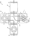
- FIG. 9 is a plan view of a plasma CVD apparatus 600 according to the sixth embodiment.
- the plasma CVD apparatus 600 includes a transfer chamber 610 disposed at a central position when viewed from above, and a plurality of chambers disposed around the transfer chamber 610, that is, a load lock chamber disposed on the left side and upstream of the drawing. 20, an intermediate layer film forming chamber 40 disposed on the upper side to form an intermediate layer, a film forming chamber 1 disposed on the lower side and having a vacuum chamber 2, on the right side of the figure and disposed on the downstream side
- the load lock chamber 30 is provided.
- the load lock chamber 20 is provided with a gate valve 65 that is a door for carrying in the substrate W
- the load lock chamber 30 is provided with a gate valve 66 that is a door for carrying out the substrate W.
- a gate valve is disposed between the transfer chamber 610 and the surrounding chambers. Specifically, a gate valve 61 is provided between the transfer chamber 610 and the load lock chamber 20, a gate valve 62 is provided between the transfer chamber 610 and the film forming chamber 1, and a film is formed between the transfer chamber 610 and the intermediate layer. A gate valve 63 is provided between the chamber 40 and a gate valve 64 is provided between the transfer chamber 610 and the load lock chamber 30 so as to be openable and closable. These gate valves make it possible to maintain the transfer chamber 610, the film formation chamber 1, and the intermediate layer film formation chamber 40 in an evacuated state during the operation of the plasma CVD apparatus 600.
- the base material W is mounted on a revolution table 5 on which six rotation tables 4 are arranged, as in the first embodiment.
- the substrate W is carried from the outside of the plasma CVD apparatus 600 to the upstream load lock chamber 20 while being mounted on the revolution table 5, and passes through the transfer chamber 610 to form the intermediate layer deposition chamber 40, the formation layer.
- the film chamber 1 is sequentially transferred to the vacuum chamber 2 and the downstream load lock chamber 30, and is carried out of the plasma CVD apparatus 600 from the downstream load lock chamber 30.
- the transfer order of the revolving table 5 is shown by white arrows in FIG.
- the transfer mechanism for the revolution table 5 is the same as or similar to the table carriage 50 shown in the first embodiment.
- the substrate W is mounted on the revolution table 5 on which the six rotation tables 4 are arranged as in the first embodiment, but the form of the table and the mounting form of the substrate W are as follows. The form shown in the other embodiments described above may be used.
- the film formation process in the plasma CVD apparatus 600 after intermediate layer film formation is performed through vacuum evacuation, film formation by plasma CVD, cooling, and taking out the substrate W to the atmosphere are sequentially performed.
- the base material W mounted on the revolution table 5 is processed as follows. In the initial state, the gate valves 61 to 66 are closed, and the transfer chamber 610, the film formation chamber 1, and the intermediate layer film formation chamber 40 are in a vacuum state.
- the gate valve 65 is opened, and the revolving table 5 on which the base material W is mounted is carried into the load lock chamber 20. Thereafter, the gate valve 65 is closed and exhausted until the load lock chamber 20 is in a vacuum state.
- the gate valve 61 and the gate valve 62 are opened, and the revolving table 5 on which the substrate W is mounted moves to the intermediate layer film forming chamber 40 via the transfer chamber 610.
- the gate valve 61 is closed.
- the load lock chamber 20 is opened to the atmosphere after the gate valve 61 is closed, and the gate valve 65 is opened to wait for the substrate W to be loaded next.
- the film supply source (sputter evaporation source) 6 operates to form an intermediate layer on the surface of the substrate W as a base of the CVD layer.
- the gate valve 62 and the gate valve 63 are opened, and the revolving table 5 on which the substrate W is mounted enters the film formation chamber 1 via the transfer chamber 610. Moving.
- the intermediate layer deposition chamber 40 waits for the substrate W to be transferred next from the load lock chamber 20.
- the two groups of base materials W mounted on the revolution table 5 are connected to both electrodes of the plasma generation power source 10, and film formation is performed while the process gas is being introduced. Done.
- the gate valve 63 and the gate valve 64 are opened, and the revolving table 5 on which the substrate W is mounted moves to the load lock chamber 30 via the transfer chamber 610. .
- the film forming chamber 1 waits for the substrate W to be transferred next from the intermediate layer film forming chamber 40.
- the gate valve 64 In the load lock chamber 30, after the gate valve 64 is closed, it waits for the two groups of base materials W mounted on the revolution table 5 to be cooled to an appropriate temperature. After the substrate W is cooled to an appropriate temperature, the atmosphere is introduced into the load lock chamber 30, the gate valve 66 is opened, and the revolving table 5 on which the substrate W is mounted is carried out of the load lock chamber 30. .
- the CVD film is formed on the base material W and the revolution table 5, but is hardly formed on the wall surface of the film forming chamber 1. Since the base material W and the base material holder are carried out to the outside of the plasma CVD apparatus 600 for each lot, film formation in the film forming chamber 1 can be kept to a minimum. As a result, even when film formation is performed on a large number of lots, the film formation chamber 1 is not contaminated, and scattering of film flakes causing defects and process fluctuations associated with formation of an insulating film do not occur.
- the film formation chamber 1 can be maintained in a vacuum state and a continuous film formation process can be performed, which enables efficient processing of a large number of lots.
- the ability to suppress 1 contamination is a very effective measure for stably operating the plasma CVD apparatus 600 for a long time.
- a plasma CVD apparatus 700 according to the seventh embodiment of the present invention shown in FIGS. 10A and 10B will be described.
- the plasma CVD apparatus 700 according to the seventh embodiment is different from the plasma CVD apparatus according to the above-described embodiment in the arrangement of the compartments and the operation of the substrate table. Other than that, it is the same as the other embodiments described above, and therefore, the same parts as those described above will not be repeated here.
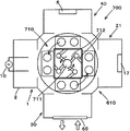
- FIG. 10A and 10B show a plasma CVD apparatus 700 according to the seventh embodiment.
- FIG. 10A is a plan view showing a state in which an arm 712 of a rotary transfer mechanism 710, which will be described later, is extended and processing is performed in the compartment
- FIG. 10B is a view of shrinking the arm 712 to transfer the substrate W from the compartment to the compartment. It is a top view which shows the state currently rotatingly transferred.
- FIG. 10C is a perspective view showing the partition plate 720 and the table 730 attached to the tip of the arm 712.
- a transfer chamber 610 disposed in the center and a plurality of chambers disposed around the transfer chamber 610 are disposed. And a separate chamber.
- a transfer chamber 610 is disposed at the center, and a heating chamber 21 is disposed on the right side, that is, the upstream side in the drawing, and an intermediate layer is formed on the upper side.
- the film forming chamber 40 is disposed, the vacuum chamber 2 of the film forming chamber 1 is disposed on the left side, that is, the downstream side, and the load lock chamber 30 is disposed on the lower side.
- the load lock chamber 30 is provided with a gate valve 65 which is a door for carrying in and carrying out the base material W.
- the arrangement of the compartments is different from the plasma CVD apparatus 700 and the plasma CVD apparatus 600. Furthermore, the following configurations are different.
- a rotational transfer mechanism 710 is disposed in the transfer chamber 610.
- This rotary transfer mechanism 710 has a rotatable central shaft 711 and four extendable arms 712 arranged at intervals of 90 ° around the center shaft 711, and a partition plate 720 is attached to the tip of this arm 712. It has been.
- FIG. 10A by extending each arm 712, each partition plate 720 can close each of the four compartment openings, and each of the four compartments has an independent atmosphere. Is possible.
- the partition plate 720 is provided with a table 730 on which the substrate W can be mounted. Further, as shown in FIG. 10B, in a state where the arm 712 is contracted, the four partition plates 720 and the table 730 can be rotated around the central axis 711 (in FIG. 10, the rotation is counterclockwise). .
- the base material W is mounted on a table 730 in which two rotation tables 4 are arranged.
- the substrate W is mounted on the rotation table 4 on the table 730 and is carried into the load lock chamber 30 from the outside of the plasma CVD apparatus 600.
- the substrate W is sequentially transferred to the heating chamber 21, the intermediate layer deposition chamber 40, the deposition chamber 1 (vacuum chamber 2), and the original load lock chamber 30 by a rotation transfer mechanism 710 provided in the transfer chamber 610.
- the load lock chamber 30 is carried out of the plasma CVD apparatus 700.
- the transfer order of the revolving table 5 is indicated by white arrows in FIG. 10A.
- two rotation tables 4 are arranged on the table 730, and the base material W is mounted on each rotation table 4.
- the table form and the base material W mounting form are different from those described above.
- the form shown in the form may be used.
- FIG. 10A shows an initial state. In this initial state, it is assumed that the gate valve 65 is in a closed state and that the substrate W for which the film forming process has been completed exists in the load lock chamber 30.
- the atmosphere is introduced into the load lock chamber 30 in a state where the load lock chamber 30 is separated from other compartments by the partition plate 720. Thereafter, the gate valve 65 is opened, the inside of the load lock chamber 30 is once opened to the atmosphere, and the substrate W after the film forming process is removed from the table 730. The next base material W is mounted on the table 730 and carried into the load lock chamber 30. Thereafter, the gate valve 65 is closed and exhausted until the load lock chamber 30 is in a vacuum state.
- the central shaft 711 rotates 90 ° counterclockwise with the arm 712 of the rotary transfer mechanism 710 contracted.
- the arm 712 of the rotation transfer mechanism 710 extends to transfer the table 730 to the heating chamber 21.
- the partition plate 720 makes the heating chamber 21 independent from other compartments (all four compartments are independent). Thereafter, the temperature of the heater 17 installed in the heating chamber 21 is increased while the rotating table 4 rotates, and the substrate W is heated.
- the central shaft 711 rotates 90 ° counterclockwise with the arm 712 of the rotary transfer mechanism 710 contracted.
- the arm 712 of the rotation transfer mechanism 710 extends to transfer the table 730 to the intermediate layer deposition chamber 40.
- the partition plate 720 makes the intermediate layer deposition chamber 40 independent from other compartments.
- the film supply source (sputter evaporation source) 6 is operated while the rotation table 4 is rotated to form an intermediate layer on the surface of the substrate W as a base of the CVD layer.
- the central shaft 711 rotates 90 ° counterclockwise with the arm 712 of the rotary transfer mechanism 710 contracted.
- the arm 712 of the rotation transfer mechanism 710 extends to transfer the table 730 to the film forming chamber 1.
- the partition plate 720 makes the film forming chamber 1 independent from other compartments.
- the two groups of base materials W are respectively connected to both electrodes of the plasma generation power source 10, and film formation is performed while introducing a process gas.
- the arm 712 of the rotary transfer mechanism 710 When film formation of the CVD layer in the film formation chamber 1 is completed, the arm 712 of the rotary transfer mechanism 710 is contracted to rotate the central shaft 711 by 90 ° counterclockwise. After completion of the rotation, the arm 712 of the rotation transfer mechanism 710 extends to transfer the table 730 to the load lock chamber 30. At this time, the partition plate 720 makes the load lock chamber 30 independent from other compartments. After this, it waits for the two groups of substrates W to be cooled to an appropriate temperature. After the substrate W is cooled to an appropriate temperature, the atmosphere is introduced into the load lock chamber 30, the gate valve 65 is opened, and the substrate W is carried out of the load lock chamber 30.
- the film formation process (evacuation ⁇ heating ⁇ intermediate layer formation ⁇ CVD layer formation by plasma CVD ⁇ cooling) performed with the gate valve 65 closed is in a state where all four compartments are in vacuum.
- the arm 712 contracts, the four partition plates 720 are drawn near the center of the transfer chamber 610 with the base material W mounted on the table 730, and in this state, the central shaft 711 rotates counterclockwise. It can be rotated 90 °. Thereafter, when the arm 712 is extended, each substrate W can be transferred to a compartment in which the next process of the film forming process is performed.
- Such a film forming process can be performed simultaneously with the base material W stored in each of the four compartments. In this way, the processing efficiency is greatly improved.
- the CVD film is hardly formed on the wall surface of the film forming chamber 1, so that the film formation in the film forming chamber 1 is minimized. Can be maintained.
- the film formation chamber 1 is not contaminated, and scattering of film flakes causing defects and process fluctuations associated with formation of an insulating film do not occur.
- the suppression of contamination of the film forming chamber 1 in this way is a very effective measure for operating the plasma CVD apparatus 700 stably and with high efficiency for a long time.
- the present invention is not limited to the above-described embodiments, and the shape, structure, material, combination, and the like of each member can be appropriately changed without changing the essence of the invention. Further, in the embodiment disclosed this time, matters that are not explicitly disclosed, for example, operating conditions and operating conditions, various parameters, dimensions, weights, volumes, and the like of a component deviate from a range that a person skilled in the art normally performs. However, matters that can be easily assumed by those skilled in the art are employed.
- an in-line type plasma CVD apparatus is difficult to deposit a CVD film on a portion other than a substrate, can be stably operated without cleaning over a long period of time, and has a high production efficiency.
- a high-pressure plasma CVD apparatus is provided.
- This in-line type plasma CVD apparatus includes a film formation chamber and a compartment different from the film formation chamber, and the substrate is transported between the film formation chamber and the compartment.
- the film forming chamber includes a vacuum chamber, a pump that exhausts air in the vacuum chamber, a gas supply unit that supplies a source gas into the vacuum chamber, and plasma is supplied to the source gas supplied into the vacuum chamber.
- An AC type plasma generating power source to be generated.
- the base material is divided into two groups, and any one of a first group connected to one electrode of the plasma generating power source and a second group connected to the other electrode of the plasma generating power source. Belongs to.
- the two groups of base materials can be configured to be flat base materials arranged opposite to each other.
- the two groups of base materials are flat base materials fixed on alternately spaced holders, or flat base materials alternately spaced.
- the two groups of substrates or substrate holders can be configured to belong to different groups alternately.
- the two groups of substrates can be configured to be mounted on a substrate holder that rotates during film formation.
- the two groups of substrates can be configured to be mounted on substrate holders that revolve and revolve during film formation.
- the two groups of base materials are mounted on a base holder that rotates and revolves, and the number of rotation tables belonging to the first group and that of the second group are the same. It can comprise so that it may be arranged by turns one by one around the revolution axis.
Landscapes
- Chemical & Material Sciences (AREA)
- Engineering & Computer Science (AREA)
- Physics & Mathematics (AREA)
- Plasma & Fusion (AREA)
- General Chemical & Material Sciences (AREA)
- Chemical Kinetics & Catalysis (AREA)
- Materials Engineering (AREA)
- Mechanical Engineering (AREA)
- Metallurgy (AREA)
- Organic Chemistry (AREA)
- Analytical Chemistry (AREA)
- Inorganic Chemistry (AREA)
- Health & Medical Sciences (AREA)
- Epidemiology (AREA)
- Public Health (AREA)
- Chemical Vapour Deposition (AREA)
Abstract
Priority Applications (3)
| Application Number | Priority Date | Filing Date | Title |
|---|---|---|---|
| CN201380068470.5A CN104903491A (zh) | 2012-12-26 | 2013-12-12 | 连续式等离子体化学气相沉积装置 |
| US14/440,728 US20150329968A1 (en) | 2012-12-26 | 2013-12-12 | In-line plasma cvd apparatus |
| EP13868944.3A EP2940183A4 (fr) | 2012-12-26 | 2013-12-12 | Dispositif de dépôt chimique en phase vapeur assisté par plasma en ligne |
Applications Claiming Priority (2)
| Application Number | Priority Date | Filing Date | Title |
|---|---|---|---|
| JP2012-282954 | 2012-12-26 | ||
| JP2012282954A JP2014125651A (ja) | 2012-12-26 | 2012-12-26 | インライン式プラズマcvd装置 |
Publications (1)
| Publication Number | Publication Date |
|---|---|
| WO2014103228A1 true WO2014103228A1 (fr) | 2014-07-03 |
Family
ID=51020352
Family Applications (1)
| Application Number | Title | Priority Date | Filing Date |
|---|---|---|---|
| PCT/JP2013/007338 Ceased WO2014103228A1 (fr) | 2012-12-26 | 2013-12-12 | Dispositif de dépôt chimique en phase vapeur assisté par plasma en ligne |
Country Status (6)
| Country | Link |
|---|---|
| US (1) | US20150329968A1 (fr) |
| EP (1) | EP2940183A4 (fr) |
| JP (1) | JP2014125651A (fr) |
| KR (1) | KR20150085085A (fr) |
| CN (1) | CN104903491A (fr) |
| WO (1) | WO2014103228A1 (fr) |
Families Citing this family (14)
| Publication number | Priority date | Publication date | Assignee | Title |
|---|---|---|---|---|
| BR102014025243B1 (pt) * | 2014-10-09 | 2022-09-27 | Mahle Metal Leve S/A | Anel de pistão para motores de combustão interna, processo para obtenção de anel de pistão e motor de combustão interna |
| BR102016007169B1 (pt) * | 2016-03-31 | 2023-01-10 | Mahle International Gmbh | Anel de pistão para motores de combustão interna, processo para obtenção de anel de pistão e motor de combustão interna |
| US11339477B2 (en) * | 2016-11-30 | 2022-05-24 | Jiangsu Favored Nanotechnology Co., LTD | Plasma polymerization coating apparatus and process |
| CN106637140B (zh) * | 2016-11-30 | 2018-08-10 | 江苏菲沃泰纳米科技有限公司 | 一种纳米镀膜设备行星回转货架装置 |
| CN106756888B (zh) | 2016-11-30 | 2018-07-13 | 江苏菲沃泰纳米科技有限公司 | 一种纳米镀膜设备旋转货架装置 |
| CN108690974A (zh) * | 2017-04-11 | 2018-10-23 | *杰有限公司 | 连续式沉积装置及连续式沉积方法 |
| CN109778151B (zh) * | 2017-11-15 | 2020-11-13 | 黄信翔 | 运用载具采逐片连续生产的化学沉积方法及设备 |
| JP6987722B2 (ja) * | 2018-09-10 | 2022-01-05 | 株式会社神戸製鋼所 | 熱フィラメントcvd装置 |
| CN109440086A (zh) * | 2018-12-14 | 2019-03-08 | 宁波易天地信远密封技术有限公司 | 一种制备高温螺栓石墨烯涂层的设备及其使用方法 |
| US11555247B2 (en) * | 2019-09-20 | 2023-01-17 | Jiangsu Favored Nanotechnology Co., Ltd. | Coating apparatus and movable electrode arrangement, movable support arrangement, and application thereof |
| CN113337809A (zh) * | 2020-02-14 | 2021-09-03 | 株式会社新柯隆 | 薄膜形成装置 |
| CN111286713B (zh) * | 2020-02-17 | 2020-10-02 | 北京科技大学 | 一种金刚石微粉的高效率处理方法与装置 |
| WO2022205480A1 (fr) * | 2021-04-02 | 2022-10-06 | 眉山博雅新材料有限公司 | Procédé de préparation de cristal composite, et système |
| TWI748922B (zh) * | 2021-05-18 | 2021-12-01 | 黃信翔 | 化學處理槽設備 |
Citations (9)
| Publication number | Priority date | Publication date | Assignee | Title |
|---|---|---|---|---|
| JPS6247486A (ja) * | 1985-08-27 | 1987-03-02 | Hitachi Ltd | 電子写真用感光体の製造装置 |
| JPH02138475A (ja) * | 1988-08-04 | 1990-05-28 | Canon Inc | マイクロ波プラズマcvd装置 |
| JPH05295551A (ja) | 1992-04-22 | 1993-11-09 | Shimadzu Corp | インライン式プラズマcvd装置 |
| JPH07297142A (ja) * | 1994-04-26 | 1995-11-10 | Canon Inc | 堆積膜形成装置及び堆積膜形成方法 |
| JP2004323883A (ja) * | 2003-04-22 | 2004-11-18 | Kobe Steel Ltd | 物理的蒸着装置 |
| JP2007308758A (ja) * | 2006-05-18 | 2007-11-29 | Denso Corp | 成膜装置及び成膜方法 |
| JP2013014818A (ja) * | 2011-07-06 | 2013-01-24 | Kobe Steel Ltd | プラズマcvd装置 |
| JP2013028851A (ja) * | 2011-07-29 | 2013-02-07 | Kobe Steel Ltd | プラズマcvd装置 |
| JP2013044047A (ja) * | 2011-08-26 | 2013-03-04 | Kobe Steel Ltd | 真空成膜装置 |
Family Cites Families (14)
| Publication number | Priority date | Publication date | Assignee | Title |
|---|---|---|---|---|
| JPS57186321A (en) * | 1981-05-12 | 1982-11-16 | Fuji Electric Corp Res & Dev Ltd | Producing method for amorphous silicon film |
| JPH0620156B2 (ja) * | 1983-06-08 | 1994-03-16 | 工業技術院長 | 太陽電池製造装置 |
| JPS62174383A (ja) * | 1986-01-28 | 1987-07-31 | Mitsubishi Chem Ind Ltd | 薄膜堆積装置 |
| JPH05209279A (ja) * | 1991-10-29 | 1993-08-20 | Canon Inc | 金属膜形成装置および金属膜形成法 |
| JP3155413B2 (ja) * | 1992-10-23 | 2001-04-09 | キヤノン株式会社 | 光受容部材の形成方法、該方法による光受容部材および堆積膜の形成装置 |
| JPH0967676A (ja) * | 1995-08-28 | 1997-03-11 | Canon Inc | 高周波プラズマcvd法による堆積膜形成装置及び堆積膜形成方法 |
| JP4089113B2 (ja) * | 1999-12-28 | 2008-05-28 | 株式会社Ihi | 薄膜作成装置 |
| JP4000830B2 (ja) * | 2001-04-27 | 2007-10-31 | コニカミノルタホールディングス株式会社 | プラズマ放電処理装置 |
| DE60226718D1 (de) * | 2002-07-08 | 2008-07-03 | Galileo Vacuum Systems S R L | Vorrichtung zur chargenweisen Vakuumbeschichtung von Gegenständen |
| US6896775B2 (en) * | 2002-10-29 | 2005-05-24 | Zond, Inc. | High-power pulsed magnetically enhanced plasma processing |
| JP2009059900A (ja) * | 2007-08-31 | 2009-03-19 | Hitachi Kokusai Electric Inc | 基板処理装置 |
| JP5036582B2 (ja) * | 2008-01-31 | 2012-09-26 | 京セラ株式会社 | 堆積膜形成方法および装置 |
| JP2009267153A (ja) * | 2008-04-25 | 2009-11-12 | Hitachi Kokusai Electric Inc | 基板処理装置および半導体装置の製造方法 |
| WO2012012394A1 (fr) * | 2010-07-23 | 2012-01-26 | First Solar, Inc | Système de dépôt en ligne |
-
2012
- 2012-12-26 JP JP2012282954A patent/JP2014125651A/ja active Pending
-
2013
- 2013-12-12 US US14/440,728 patent/US20150329968A1/en not_active Abandoned
- 2013-12-12 EP EP13868944.3A patent/EP2940183A4/fr not_active Withdrawn
- 2013-12-12 CN CN201380068470.5A patent/CN104903491A/zh active Pending
- 2013-12-12 KR KR1020157016558A patent/KR20150085085A/ko not_active Ceased
- 2013-12-12 WO PCT/JP2013/007338 patent/WO2014103228A1/fr not_active Ceased
Patent Citations (9)
| Publication number | Priority date | Publication date | Assignee | Title |
|---|---|---|---|---|
| JPS6247486A (ja) * | 1985-08-27 | 1987-03-02 | Hitachi Ltd | 電子写真用感光体の製造装置 |
| JPH02138475A (ja) * | 1988-08-04 | 1990-05-28 | Canon Inc | マイクロ波プラズマcvd装置 |
| JPH05295551A (ja) | 1992-04-22 | 1993-11-09 | Shimadzu Corp | インライン式プラズマcvd装置 |
| JPH07297142A (ja) * | 1994-04-26 | 1995-11-10 | Canon Inc | 堆積膜形成装置及び堆積膜形成方法 |
| JP2004323883A (ja) * | 2003-04-22 | 2004-11-18 | Kobe Steel Ltd | 物理的蒸着装置 |
| JP2007308758A (ja) * | 2006-05-18 | 2007-11-29 | Denso Corp | 成膜装置及び成膜方法 |
| JP2013014818A (ja) * | 2011-07-06 | 2013-01-24 | Kobe Steel Ltd | プラズマcvd装置 |
| JP2013028851A (ja) * | 2011-07-29 | 2013-02-07 | Kobe Steel Ltd | プラズマcvd装置 |
| JP2013044047A (ja) * | 2011-08-26 | 2013-03-04 | Kobe Steel Ltd | 真空成膜装置 |
Non-Patent Citations (1)
| Title |
|---|
| See also references of EP2940183A4 |
Also Published As
| Publication number | Publication date |
|---|---|
| EP2940183A4 (fr) | 2016-09-07 |
| JP2014125651A (ja) | 2014-07-07 |
| KR20150085085A (ko) | 2015-07-22 |
| US20150329968A1 (en) | 2015-11-19 |
| EP2940183A1 (fr) | 2015-11-04 |
| CN104903491A (zh) | 2015-09-09 |
Similar Documents
| Publication | Publication Date | Title |
|---|---|---|
| WO2014103228A1 (fr) | Dispositif de dépôt chimique en phase vapeur assisté par plasma en ligne | |
| CN103649370B (zh) | 真空成膜装置 | |
| US20140318454A1 (en) | Plasma cvd apparatus | |
| CA2509952A1 (fr) | Depot de couches active par plasma | |
| EP3717674A1 (fr) | Appareil de dépôt, procédé de revêtement d'un substrat souple et substrat souple muni d'un revêtement | |
| TW201901733A (zh) | 用於旋轉基座的電漿源 | |
| WO2022070922A1 (fr) | Dispositif de dépôt de film et procédé de dépôt de film | |
| JP5634962B2 (ja) | 真空成膜装置 | |
| CN102230163A (zh) | 镀膜装置 | |
| JP2008069402A (ja) | スパッタリング装置及びスパッタリング方法 | |
| CN101962754B (zh) | 镀膜装置 | |
| JP5634954B2 (ja) | プラズマcvd装置 | |
| WO2014103318A1 (fr) | Procédé de formation de film de protection à l'aide d'un procédé cvd assisté par plasma | |
| JP6768087B2 (ja) | フレキシブル基板を被覆するための堆積装置、フレキシブル基板を被覆する方法、及び被覆を有するフレキシブル基板 | |
| JP3735462B2 (ja) | 金属酸化物光学薄膜の形成方法および成膜装置 | |
| KR101413981B1 (ko) | 플라즈마 발생장치 및 이를 포함하는 박막증착장치 | |
| JP6005536B2 (ja) | アーク蒸発源を備えたプラズマcvd装置 | |
| JP7186234B2 (ja) | 堆積装置、フレキシブル基板をコーティングする方法、及びコーティングを有するフレキシブル基板 | |
| WO2020170577A1 (fr) | Appareil de formation de film par pulvérisation, procédé de formation de film par pulvérisation associé, et film mince composite | |
| TWI841863B (zh) | 表面處理裝置及表面處理方法 | |
| KR100502000B1 (ko) | 플라스틱 제품의 진공증착 코팅장치 | |
| KR20120061013A (ko) | 리니어 cvd 소스 및 전자빔 스퍼터를 이용한 입체상 중합체의 금속박막 형성장치 및 형성방법 | |
| KR101384980B1 (ko) | 플라즈마 발생장치 및 이를 포함하는 박막증착장치 | |
| JP3180557U (ja) | 薄膜作製装置 | |
| CN117940604A (zh) | 表面处理装置以及表面处理方法 |
Legal Events
| Date | Code | Title | Description |
|---|---|---|---|
| 121 | Ep: the epo has been informed by wipo that ep was designated in this application |
Ref document number: 13868944 Country of ref document: EP Kind code of ref document: A1 |
|
| WWE | Wipo information: entry into national phase |
Ref document number: 14440728 Country of ref document: US |
|
| REEP | Request for entry into the european phase |
Ref document number: 2013868944 Country of ref document: EP |
|
| WWE | Wipo information: entry into national phase |
Ref document number: 2013868944 Country of ref document: EP |
|
| ENP | Entry into the national phase |
Ref document number: 20157016558 Country of ref document: KR Kind code of ref document: A |
|
| NENP | Non-entry into the national phase |
Ref country code: DE |