WO2014103265A1 - Amplificateur de puissance - Google Patents
Amplificateur de puissance Download PDFInfo
- Publication number
- WO2014103265A1 WO2014103265A1 PCT/JP2013/007492 JP2013007492W WO2014103265A1 WO 2014103265 A1 WO2014103265 A1 WO 2014103265A1 JP 2013007492 W JP2013007492 W JP 2013007492W WO 2014103265 A1 WO2014103265 A1 WO 2014103265A1
- Authority
- WO
- WIPO (PCT)
- Prior art keywords
- current
- group
- power amplifier
- switches
- current sources
- Prior art date
- Legal status (The legal status is an assumption and is not a legal conclusion. Google has not performed a legal analysis and makes no representation as to the accuracy of the status listed.)
- Ceased
Links
Images





Classifications
-
- H—ELECTRICITY
- H03—ELECTRONIC CIRCUITRY
- H03F—AMPLIFIERS
- H03F3/00—Amplifiers with only discharge tubes or only semiconductor devices as amplifying elements
- H03F3/20—Power amplifiers, e.g. Class B amplifiers, Class C amplifiers
- H03F3/21—Power amplifiers, e.g. Class B amplifiers, Class C amplifiers with semiconductor devices only
- H03F3/211—Power amplifiers, e.g. Class B amplifiers, Class C amplifiers with semiconductor devices only using a combination of several amplifiers
-
- H—ELECTRICITY
- H03—ELECTRONIC CIRCUITRY
- H03F—AMPLIFIERS
- H03F3/00—Amplifiers with only discharge tubes or only semiconductor devices as amplifying elements
- H03F3/20—Power amplifiers, e.g. Class B amplifiers, Class C amplifiers
- H03F3/21—Power amplifiers, e.g. Class B amplifiers, Class C amplifiers with semiconductor devices only
- H03F3/217—Class D power amplifiers; Switching amplifiers
- H03F3/2178—Class D power amplifiers; Switching amplifiers using more than one switch or switching amplifier in parallel or in series
-
- H—ELECTRICITY
- H03—ELECTRONIC CIRCUITRY
- H03F—AMPLIFIERS
- H03F3/00—Amplifiers with only discharge tubes or only semiconductor devices as amplifying elements
- H03F3/20—Power amplifiers, e.g. Class B amplifiers, Class C amplifiers
- H03F3/24—Power amplifiers, e.g. Class B amplifiers, Class C amplifiers of transmitter output stages
- H03F3/245—Power amplifiers, e.g. Class B amplifiers, Class C amplifiers of transmitter output stages with semiconductor devices only
-
- H—ELECTRICITY
- H03—ELECTRONIC CIRCUITRY
- H03F—AMPLIFIERS
- H03F2200/00—Indexing scheme relating to amplifiers
- H03F2200/18—Indexing scheme relating to amplifiers the bias of the gate of a FET being controlled by a control signal
-
- H—ELECTRICITY
- H03—ELECTRONIC CIRCUITRY
- H03F—AMPLIFIERS
- H03F2200/00—Indexing scheme relating to amplifiers
- H03F2200/432—Two or more amplifiers of different type are coupled in parallel at the input or output, e.g. a class D and a linear amplifier, a class B and a class A amplifier
-
- H—ELECTRICITY
- H03—ELECTRONIC CIRCUITRY
- H03F—AMPLIFIERS
- H03F2203/00—Indexing scheme relating to amplifiers with only discharge tubes or only semiconductor devices as amplifying elements covered by H03F3/00
- H03F2203/20—Indexing scheme relating to power amplifiers, e.g. Class B amplifiers, Class C amplifiers
- H03F2203/21—Indexing scheme relating to power amplifiers, e.g. Class B amplifiers, Class C amplifiers with semiconductor devices only
- H03F2203/211—Indexing scheme relating to power amplifiers, e.g. Class B amplifiers, Class C amplifiers with semiconductor devices only using a combination of several amplifiers
- H03F2203/21109—An input signal being distributed by switching to a plurality of paralleled power amplifiers
-
- H—ELECTRICITY
- H03—ELECTRONIC CIRCUITRY
- H03F—AMPLIFIERS
- H03F2203/00—Indexing scheme relating to amplifiers with only discharge tubes or only semiconductor devices as amplifying elements covered by H03F3/00
- H03F2203/20—Indexing scheme relating to power amplifiers, e.g. Class B amplifiers, Class C amplifiers
- H03F2203/21—Indexing scheme relating to power amplifiers, e.g. Class B amplifiers, Class C amplifiers with semiconductor devices only
- H03F2203/211—Indexing scheme relating to power amplifiers, e.g. Class B amplifiers, Class C amplifiers with semiconductor devices only using a combination of several amplifiers
- H03F2203/21136—An input signal of a power amplifier being on/off switched
-
- H—ELECTRICITY
- H03—ELECTRONIC CIRCUITRY
- H03F—AMPLIFIERS
- H03F2203/00—Indexing scheme relating to amplifiers with only discharge tubes or only semiconductor devices as amplifying elements covered by H03F3/00
- H03F2203/20—Indexing scheme relating to power amplifiers, e.g. Class B amplifiers, Class C amplifiers
- H03F2203/21—Indexing scheme relating to power amplifiers, e.g. Class B amplifiers, Class C amplifiers with semiconductor devices only
- H03F2203/211—Indexing scheme relating to power amplifiers, e.g. Class B amplifiers, Class C amplifiers with semiconductor devices only using a combination of several amplifiers
- H03F2203/21145—Output signals are combined by switching a plurality of paralleled power amplifiers to a common output
-
- H—ELECTRICITY
- H03—ELECTRONIC CIRCUITRY
- H03F—AMPLIFIERS
- H03F2203/00—Indexing scheme relating to amplifiers with only discharge tubes or only semiconductor devices as amplifying elements covered by H03F3/00
- H03F2203/20—Indexing scheme relating to power amplifiers, e.g. Class B amplifiers, Class C amplifiers
- H03F2203/21—Indexing scheme relating to power amplifiers, e.g. Class B amplifiers, Class C amplifiers with semiconductor devices only
- H03F2203/211—Indexing scheme relating to power amplifiers, e.g. Class B amplifiers, Class C amplifiers with semiconductor devices only using a combination of several amplifiers
- H03F2203/21184—Indexing scheme relating to power amplifiers, e.g. Class B amplifiers, Class C amplifiers with semiconductor devices only using a combination of several amplifiers the supply current of a power amplifier being continuously measured, e.g. by a resistor, a current mirror, to produce a controlling signal
-
- H—ELECTRICITY
- H03—ELECTRONIC CIRCUITRY
- H03F—AMPLIFIERS
- H03F3/00—Amplifiers with only discharge tubes or only semiconductor devices as amplifying elements
- H03F3/04—Amplifiers with only discharge tubes or only semiconductor devices as amplifying elements with semiconductor devices only
-
- H—ELECTRICITY
- H03—ELECTRONIC CIRCUITRY
- H03F—AMPLIFIERS
- H03F3/00—Amplifiers with only discharge tubes or only semiconductor devices as amplifying elements
- H03F3/34—DC amplifiers in which all stages are DC-coupled
- H03F3/343—DC amplifiers in which all stages are DC-coupled with semiconductor devices only
- H03F3/345—DC amplifiers in which all stages are DC-coupled with semiconductor devices only with field-effect devices
Definitions
- the present invention relates to a power amplifier.
- a power amplifier as a circuit that outputs a large amplitude signal to radiate radio waves from an antenna.
- the output of the power amplifier is a signal that is close to the pulse waveform and includes harmonic components.
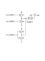
- FIG. 12 is a circuit diagram of the power amplifier described in Patent Document 1
- FIG. 13 is a timing chart showing signal waveforms of respective parts of the power amplifier of FIG.
- the power amplifier of FIG. 12 includes an output of an inverter composed of an N channel type MOS transistor 1001 and a P channel type MOS transistor 1002, and an inverter composed of an N channel type MOS transistor 1003 and a P channel type MOS transistor 1004.
- the output signal is synthesized from the output.
- the timing signals A10, B10, and C10 to the respective parts are set independently in duty ratio and phase, thereby suppressing the odd harmonics by bringing the output waveform closer to a sine wave.
- the power amplifier of FIG. 12 requires a timing generation circuit that generates a plurality of timing signals A10, B10, and C10 having different duty ratios in order to suppress harmonics.
- the timing generation circuit is a circuit in which logic circuits such as an AND circuit or an OR circuit are combined. For this reason, in the timing generation circuit, the higher the signal frequency, the greater the influence of delay due to elements and wiring, and the timing of rising and falling of the timing signal deviates from ideal. Therefore, the power amplifier of FIG. 12 has a problem that the amount of suppression of odd-order harmonics deteriorates due to timing signal deviation.
- An object of the present invention is to provide a power amplifier that can easily suppress odd-order harmonics even when the frequency is high.
- a power amplifier includes n (n is a natural number of 3 or more) current sources for supplying a predetermined current, n switches for opening and closing current paths of the n current sources, a timing signal generator for outputting n timing signals for turning on / off each of the n switches, wherein the n timing signals are signals having the same duty ratio and different phases.
- n is a natural number of 3 or more
- n switches for opening and closing current paths of the n current sources
- a timing signal generator for outputting n timing signals for turning on / off each of the n switches, wherein the n timing signals are signals having the same duty ratio and different phases.
- a configuration is adopted in which a signal whose power is amplified based on the current flowing through the n current sources is output.
- Configuration diagram of a power amplifier according to Embodiment 1 of the present invention Timing chart showing operation of power amplifier in embodiment 1 of the present invention
- Conceptual diagram of a power amplifier according to Embodiment 1 of the present invention The block diagram of the modification of Embodiment 1 of this invention Schematic diagram illustrating the size of the MOS transistor of FIG.
- Configuration diagram of power amplifier according to Embodiment 2 of the present invention Timing chart showing operation of power amplifier in embodiment 2 of the present invention
- Configuration diagram of power amplifier in Embodiment 3 of the present invention Timing chart showing operation of power amplifier in embodiment 3 of the present invention
- Configuration of conventional power amplifier Configuration diagram of first example of conventional inverter type power amplifier
- Configuration diagram of second example of conventional inverter type power amplifier Timing chart showing operation of second example of conventional inverter type power amplifier
- FIG. 1 is a configuration diagram of a power amplifier according to Embodiment 1 of the present invention.
- the power amplifier includes a reference current source 108, a plurality of NMOS transistors (N-channel Metal-Oxide-Semiconductor Field-Effect Transistors) 100 to 103 constituting a current mirror circuit. , A plurality of NMOS transistors 104 to 107 as switches, a pull-up coil 109, a band-pass filter 110, and a timing signal generator 114.
- the power amplifier has an output terminal connected to the antenna 111 and outputs a large-amplitude current to the antenna 111.
- the reference current source 108 and the NMOS transistors 100, 101, 102, and 103 constitute a current mirror circuit.
- the reference current source 108 is a constant current source, for example.
- the NMOS transistors 101, 102, and 103 transfer the current flowing through the transfer source NMOS transistor 100 at a predetermined mirror ratio and flow through the NMOS transistor 101 when a voltage of a certain level or higher is applied between the drain and the source.
- These three sets of current mirror circuits ((100, 101), (100, 102), (100, 103)) correspond to three current sources.
- the drain terminals of the NMOS transistors 101, 102, and 103 are connected to the pull-up terminal of the coil 109 and the input terminal of the band pass filter 110.
- the other end of the band pass filter 110 is an output terminal of the power amplifier, and this output terminal is connected to the antenna 111.
- NMOS transistors 105, 106, and 107 are switches that are turned on / off by timing signals A, B, and C sent from the timing signal generator 114.
- the NMOS transistors 105, 106, and 107 are respectively connected between the source terminals of the NMOS transistors 101, 102, and 103 that pass a transfer current and the ground, and open and close these current paths.
- the NMOS transistor 104 of the transfer source circuit is a dummy switch for making the characteristics of the transfer destination and the transfer source the same, and is always turned on.
- NMOS transistors 101, 102 and 103 the ratio of the current flowing in itself 1: 2 1/2: to be 1, the W / L ratio of the NMOS transistors 101, 102, and 103 1: 2 1/2: 1 Formed.
- W represents the gate width of the transistor
- L represents the gate length.
- the timing signal generator 114 generates timing signals A, B, and C for turning on / off the NMOS transistors 105, 106, and 107 that are switches.
- the timing signal generator 114 modulates the frequency of the timing signals A, B, and C according to the input signal, thereby modulating the frequency of the output current of the power amplifier.
- the coil 109 has a sufficiently small resistance for direct current and a sufficiently large resistance for high frequency. During operation of the power amplifier, the coil 109 supplies a direct current to the circuit from the power supply line VDD. The summed output current IT flowing through the NMOS transistors 101, 102, 103 flows through the coil 109 only in the DC component, and the high frequency component is output to the antenna 111 via the band pass filter 110.
- FIG. 2 is a timing chart showing the operation of the power amplifier according to the first embodiment.
- the timing signal A, the timing signal B, and the timing signal C are all signals having a duty ratio of 50% and a phase difference of 45 degrees.
- the timing signal A is a signal that rises at a phase of 0 degree
- the timing signal B rises at a phase of -45 degrees
- the timing signal C rises at a phase of -90 degrees.
- the timing signal A, the timing signal B, and the timing signal C have the same high level voltage value.
- the output currents IA, IB, and IC flowing through the drain terminals of the NMOS transistors 101, 102, and 103 have waveforms that have a predetermined current value during the high-level period of the timing signals A, B, and C, respectively.
- the W / L ratio of the NMOS transistors 101, 102, 103 is set to 1: 2 1/2 : 1
- the magnitudes of the output currents IA, IB, IC are 1: 2 1/2. : 1.
- the output current IT is a sum of the output currents IA, IB and IC, and a high frequency component is output to the antenna 111 via the band pass filter 110.
- the relationship between the third and fifth harmonics of the output currents IA, IB, and IC is that the phase of the timing signal A, timing signal B, and timing signal C is shifted by 45 degrees, so the output current IA and the output current IC are added.
- the relationship between the current and the output current IB is reversed.
- the amplitude of the output current IB is 21/2 times that of the output current IA, it is equal to the amplitude of the current obtained by adding the output current IA and the output current IC. Therefore, the third and fifth harmonics of the output currents IA, IB and IC cancel each other. When the waveform of the output current IT is viewed in the spectrum, it can be seen that the third and fifth harmonic components are suppressed.
- the power amplifier according to the first embodiment since the power amplifier according to the first embodiment has an open drain configuration, large power can be output by setting a large voltage amplitude of the output signal.
- FIG. 1 The configuration specifically shown in FIG. 1 can be variously changed.
- FIG. 3 is a conceptual diagram of the power amplifier according to the first embodiment of the present invention.
- the power amplifier of FIG. 1 uses three sets of current mirror circuits ((100, 101), (100, 102), (100, 103)) as three current sources. As shown, various current sources 301, 302, 303 having similar functions may be used. 1 uses three NMOS transistors 105, 106, and 107 as three switches. For example, various elements 304, 305, and 306 having similar functions such as bipolar transistors are used. May be.
- FIG. 4 is a configuration diagram of a current amplifier according to a modification of the first embodiment.
- the current amount of the reference current source 108 is fixed.
- the current amount of the reference current source 108 can be adjusted by a current value control signal. Also good.
- the amplitude of the output current T can be changed. The change in amplitude can be used for signal level switching or amplitude modulation of a transmission signal.
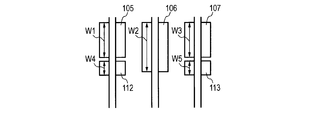
- FIG. 5 is a schematic diagram for explaining the size of the NMOS transistor of FIG.
- the NMOS transistors 104, 105, 106, and 107 that are switches should be designed to have a channel size that matches the ratio of the current values in order to make the current densities of the currents flowing through the NMOS transistors 104, 105, 106, and 107 the same.
- the gate widths W1, W2, and W3 of the NMOS transistors 105, 106, and 107 are set to 1: 2 1/2 : 1 (in accordance with the current ratio 1: 2 1/2 : 1.
- the gate length should be constant).
- the gate loads (parasitic capacitances) of the NMOS transistors 105, 106, and 107 that are switches are not constant. Therefore, when the timing signals A, B, and C are generated under the same conditions, the rising and falling waveforms of the timing signals A, B, and C change, and the NMOS transistors 105, 106, and 107 are turned on / off. There is a risk of errors in timing.
- the configuration of FIG. 5 is a configuration having load adjustment MOS transistors 112 and 113 of a size that fills the size difference in correspondence with the small size NMOS transistors 105 and 107.
- the gate terminals of the NMOS transistors 105 and 107 and the load adjustment MOS transistors 112 and 113 are connected to each other.
- the source terminals and drain terminals of the load adjustment MOS transistors 112 and 113 are connected to the same potential point (for example, ground) so that no current flows through the load adjustment MOS transistors 112 and 113.
- the gate widths W4 and W5 of the load adjustment MOS transistors 112 and 113 may be set as W1 + W4 ⁇ W2 ⁇ W3 + W5, for example, with the same gate length as the NMOS transistors 105, 106, and 107.
- the loads (capacitances) of the three gate lines of the NMOS transistors 105, 106, and 107 as viewed from the timing signal generation unit 114 are substantially equal.
- the timing signals A, B, and C generated under the same conditions can turn on / off the NMOS transistors 105, 106, and 107 without timing errors.
- FIG. 6 is a configuration diagram of the power amplifier according to the second embodiment of the present invention.
- the same components as those in FIG. 6 are identical to FIG. 6, the same components as those in FIG.
- the power amplifier according to the second embodiment has the same configuration as that of the non-inverting unit (corresponding to the first group) 120 which is a part of the circuit of FIG. And an inversion unit (corresponding to the second group) 430 operating in the opposite phase, capacitors 410 and 419, and a balun 420.
- the inverting unit 430 includes three NMOS transistors 401, 402, and 403 that constitute a current mirror circuit, three NMOS transistors 405, 406, and 407 that are switches, and a coil 418 for pull-up. These have the same configuration as that of the non-inverting unit 120 except that they operate in opposite phases.
- the reference current source 108 and the NMOS transistor 100 through which the transfer source reference current flows are shared by the inversion unit 430 and the non-inversion unit 120. That is, the gate terminals of the NMOS transistors 401, 402, and 403, which are current sources in the inverting unit 430, are connected to the gate terminal of the NMOS transistor 100 that supplies the reference current.
- Capacitors 410 and 419 connect the output terminals of both the non-inverting unit 120 and the inverting unit 430 in a high frequency manner.
- a high-frequency component of the differential current between the output current T4a of the non-inverting unit 120 and the output current T4b of the inverting unit 430 flows through the signal line connecting the capacitors 410 and 419.
- the reason why the capacitors 410 and 419 are connected to the output terminals of both the non-inverting unit 120 and the inverting unit 430 is to make the configurations of the non-inverting unit 120 and the inverting unit 430 symmetrical.
- a balun (balanced-unbalanced converter) 420 is configured to couple a signal line through which a differential current flows between the non-inverting unit 120 and the inverting unit 430 and an input signal line of the bandpass filter 110 in a high frequency manner.
- the output signals of 120 and inverting unit 430 are sent to band pass filter 110.
- the timing signal generator 114 turns on / off the NMOS transistors 105, 106, 107 of the non-inverting unit 120, and turns on / off the NMOS transistors 405, 406, 407 of the inverting unit 430. Signals D, E, and F are generated.
- the drain terminals of the NMOS transistors 401, 402, and 403 are connected to the other terminal of the pull-up coil 418 whose one terminal is connected to the power supply line VDD and one terminal of the capacitor 419.
- the other terminal of the capacitor 419 is connected to one terminal on the balanced side of the balun 420.
- the other terminal of the capacitor 410 having one terminal connected to the drain terminals of the NMOS transistors 101, 102, and 103 is connected to the other terminal on the balanced side of the balun 420.
- the input terminal of the band pass filter 110 is connected to the unbalanced terminal of the balun 420, and the antenna 111 is connected to the output terminal of the band pass filter 110.
- the NMOS transistors 101, 102, 103, 401, 402, and 403 have a W / L ratio so that a current ratio flowing through the NMOS transistors 101, 102, 103, 401, 402, and 403 is 1: 2 1/2 : 1: 1: 2 1/2 : 1. Is formed to 1: 2 1/2 : 1: 1: 2 1/2 : 1.
- W represents the gate width of the transistor
- L represents the gate length.
- FIG. 7 is a timing chart showing the operation of the power amplifier according to the second embodiment.
- Timing signal A, timing signal B, timing signal C, timing signal D, timing signal E, and timing signal F all have a duty ratio of 50%, and the phase relationship is as follows.
- Timing signal A phase timing signal D phase + 180 degrees
- Timing signal B phase timing signal E phase + 180 degrees
- Timing signal C phase timing signal F phase + 180 degrees
- Timing signal A, timing signal B, timing signal C, timing signal D, timing signal E, and timing signal F are signals for turning on / off NMOS transistors 105, 106, 107, 405, 406, and 407, in order.
- the phase is shifted by 45 degrees.
- the timing signal A is 0 degree
- the timing signal B is -45 degrees
- the timing signal C is -90 degrees
- the timing signal D is -180 degrees
- the timing signal E is -225 degrees
- the timing signal F is -270 degrees. Is off.
- the currents flowing through the drain terminals of the NMOS transistors 101, 102, 103, 401, 402, and 403 are output current IA, output current IB, output current IC, output current ID, output current IE, and output current. It becomes a waveform like IF.
- the W / L ratio of the NMOS transistor is set to 1: 2 1/2 : 1: 1: 2 1/2 : 1, the current is also 1: 2 1/2 : 1: 1: 2. 1/2 : 1.
- the output current T4a is the sum of the currents of the NMOS transistors 101, 102, and 103
- the output current T4b is the sum of the currents of the NMOS transistors 401, 402, and 403.
- the output current T4c is a waveform after being converted from a balanced signal to an unbalanced signal by the balun 420.
- the waveform of the output current T4c is seen in the spectrum, the third-order and fifth-order harmonic components are suppressed as in the first embodiment, and the even-order harmonic components are suppressed by the differentiation.
- even-order harmonic components can be suppressed by differentiation.
- the non-inverting unit 120 and the inverting unit 430 that operate in opposite phases have the same configuration, the relative variation of elements between them is reduced, thereby suppressing even-order harmonic components satisfactorily. be able to.
- the output of the power can be increased by the differentiation as compared with the inverter type power amplifier using the NMOS transistor and the PMOS (P channel type MOS) transistor.
- FIG. 8 is a configuration diagram of the power amplifier according to the third embodiment of the present invention.
- the same components as those in FIG. 8 are identical to FIG. 8 and the same components as those in FIG. 8.
- the power amplifier according to the third embodiment is obtained by adding a harmonic suppression circuit 610 for suppressing the secondary harmonic component in addition to the same configuration as that of FIG.
- the harmonic suppression circuit 610 includes a plurality of sets of NMOS transistors 612, 613, 614, 615, and a switch group 621. Although only two sets of NMOS transistors 612, 613, 614, 615 and switches 616, 617 of the switch group 621 are illustrated in FIG. 8, a large number of sets, such as 4, 8, 16, 32, are provided. May be. Moreover, it is good also as only one set.
- NMOS transistors (corresponding to current sources for suppressing harmonics) 612 and 613 are connected to the NMOS transistor 100 through which the reference current flows and the gate terminals of each other to constitute a current mirror circuit.
- the NMOS transistors 614 and 615 flow a corrective current for suppressing harmonics, and the current value is smaller than the current flowing through the NMOS transistors 101, 102, and 103.
- NMOS transistors (corresponding to harmonic suppression switches) 614 and 615 are connected between the source terminals of the NMOS transistors 612 and 613 serving as current sources and the ground, and function as switches for opening and closing the current path.
- the switch group (corresponding to the number switching means) 621 includes a plurality of switches 616 and 617 that individually switch between the operation and non-operation of the plurality of sets of NMOS transistors 612, 613, 614, and 615. Specifically, the switches 616 and 617 open and close the signal lines that send the timing signal K to the gate terminals of the NMOS transistors 614 and 615, respectively. The plurality of switches 616 and 617 are switched by a switch switching control signal. When the switches 616 and 617 are open, the gate terminals of the NMOS transistors 614 and 615 are connected to the ground so that the voltage at the gate terminals does not become unstable.
- the timing signal generator 114 generates a timing signal K in addition to the timing signals A to C.
- the timing signal generation unit 114 outputs the timing signal K to the harmonic suppression circuit 610.
- the timing signal K corresponds to a harmonic suppression timing signal.
- the specific connection and configuration of the harmonic suppression circuit 610 are as follows.
- the drain terminals of the NMOS transistors 612 and 613 are connected to the input terminal of the band pass filter 110.
- the output currents IG and IH flowing through the NMOS transistors 612 and 613 are added to the summed output current (IA + IB + IC) of the NMOS transistors 101, 102, and 103 to correct the output current T6 of the power amplifier.
- the currents flowing through the plurality of NMOS transistors 612 and 613 of the harmonic suppression circuit 610 are set to increase in order of powers of 2, for example. For example, in the case of four, it is set to increase at 1: 2: 4: 8. With such a setting, the current value applied from the harmonic suppression circuit 610 to the output current T6 is switched in multiple stages at regular intervals by individually switching the operation / non-operation of the plurality of NMOS transistors 612 and 613. Can do.
- the W / L ratio of the plurality of NMOS transistors 612 and 613 is set to a ratio that increases in order of a power of 2.
- the W / L ratio of the NMOS transistors 612 and 613 is set independently of the W / L ratio of the NMOS transistors 101, 102, and 103 that output most of the output current of the power amplifier. That is, the current amplitudes Y and S in FIG. 9 are set independently.
- the current amplitude S is sufficiently smaller than the current amplitude Y.
- the timing signals G and H for turning on / off the NMOS transistors 612 and 613 are selected to be output / stopped by switching the switches 616 and 617.
- the amount of current corrected by the harmonic suppression circuit 610 is changed, and the amount of current for removing harmonics is selected according to the content of the second harmonic that varies at each time point or for each individual device. be able to.
- the correction current harmonic suppression circuit 610 can be switched in two 4 stages.
- Timing signals G and H are signals sent from the timing signals K generated by the timing signal generator 114 to the gate terminals of the NMOS transistors 614 and 615 through the switches 616 and 617. Therefore, these timing signals G and H are in-phase signals.
- FIG. 9 is a timing chart showing the operation of the power amplifier according to the third embodiment.
- Timing signal A, timing signal B, timing signal C, timing signal G, and timing signal H are signals for turning on / off NMOS transistors 105, 106, 107, 614, and 615, and have the same amplitude. But the phase and frequency are different.
- Timing signal A, timing signal B, and timing signal C are signals having the same frequency and sequentially shifted in phase by 45 degrees.
- Timing signals G and H are signals having the same phase and a duty ratio of 50%.
- the phases of the timing signal G and the timing signal H are set so that the output current IG and the output current IH are opposite in phase to the harmonic of twice the signal obtained by adding the output current IA, the output current IB, and the output current IC. Is done.
- the rising phase of the timing signal A is 0 degree
- the rising phase of the timing signal B is -45 degrees
- the rising phase of the timing signal C is -90 degrees
- the rising phase of the timing signal G is 0 degrees
- the rising phase of the timing signal H Is 0 degrees.
- the frequency of the timing signal G and the timing signal H is twice the frequency of the timing signal A, the timing signal B, and the timing signal C.
- the output current IA, the output current IB, the output current IC, the output current IG, and the output current IH flowing through the drain terminals of the NMOS transistors 101, 102, 103, 612, and 613 have waveforms as shown in FIG. Since the W / L ratios of the NMOS transistors 101, 102, 103, 612, and 613 are set to Y: ( 21/2 ⁇ Y): Y: S: (2 ⁇ S), the current is also Y :( 2 1/2 ⁇ Y): Y: S: (2 ⁇ S). Here, the Y value and the S value are set independently.
- the output current T6 has a waveform obtained by adding the currents of the NMOS transistors 101, 102, 103, 612, and 613.
- the waveform of the output current T6 is seen in the spectrum, the third-order and fifth-order harmonic components are suppressed in the same manner as in the first embodiment, and a signal having the opposite phase of the double harmonic is added. It can be seen that the second-order harmonic component is suppressed.
- the open drain configuration can output higher power than an inverter type power amplifier using an NMOS transistor and a PMOS transistor.
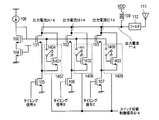
- FIG. 14 is a configuration diagram of the power amplifier according to the fourth embodiment of the present invention.
- the power amplifier according to the fourth embodiment has fine adjustment circuits 1407, 1408, 1409 in order to improve the degradation of the suppression amount of the harmonic component due to element variation in addition to the configuration similar to FIG. 1. Is added.
- Fine adjustment circuits 1407, 1408, 1409 are composed of NMOS transistors 1401, 1402, 1403 and switches 1404, 1405, 1406.
- the switches 1404, 1405, and 1406 When the switches 1404, 1405, and 1406 are on, the NMOS transistor 100 through which the reference current flows and the gate terminals of each other are connected to form a current mirror circuit.
- the switches 1404, 1405, and 1406 When the switches 1404, 1405, and 1406 are off, the gate terminals of the NMOS transistors 1401, 1402, and 1403 are connected to the ground so that the voltage at the gate terminals does not become unstable. Further, by turning on / off the switches 1404, 1405, and 1406, the currents flowing through the output currents IA14, IB14, and IC14 can be adjusted. Individual switches are independently switched by a switch switching control signal S14.
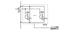
- FIG. 15 shows a case where a plurality of transistors and switches are used in the fine adjustment circuit 1407 in FIG.
- the fine adjustment circuit 1407a is configured such that the transistor 1401a is connected in parallel to the NMOS transistor 1401, and the switches 1404 and 1404a are connected to the respective gates.
- the W / L ratio of the NMOS transistors 1401 and 1401a is set to a ratio that increases in order of a power of 2, so that each switch can be turned on / off independently.
- the amount of current corrected by the fine adjustment circuit 1407a can be changed, and the amount of current for removing harmonics can be selected in accordance with the content of harmonics varying at each time point or for each individual device.
- the correction current of the fine adjustment circuit 1407a can be switched in 24 stages by a 4-bit switch switching control signal S15.
- the fine adjustment circuit 1407 of FIG. 14 has been described as an example. However, when the adjustment range is large and the adjustment accuracy is high, the fine adjustment circuits 1408 and 1409 are similarly provided with a plurality of transistors of the fine adjustment circuit and switched by a switch. To be able to.
- the current amplitude of the constant current source can be finely adjusted, and the current amplitude error due to element variation and the constant current source are turned on / off. It is possible to improve deterioration of the suppression amount of the harmonic component due to the phase error of the control signal.
- Each block used in the description of the above embodiment is typically realized as an IC which is an integrated circuit. These may be individually made into one chip, or may be made into one chip so as to include a part or all of them. Although referred to here as an IC, it may be referred to as an LSI, a system LSI, a super LSI, or an ultra LSI depending on the degree of integration.
- the method of circuit integration is not limited to IC, and may be realized by a dedicated circuit.
- An FPGA Field Programmable Gate Array
- a reconfigurable processor that can reconfigure the connection and setting of circuit cells inside the LSI may be used.
- the present invention is useful, for example, for a power amplifier that drives an antenna.
Landscapes
- Engineering & Computer Science (AREA)
- Power Engineering (AREA)
- Amplifiers (AREA)
- Logic Circuits (AREA)
Abstract
Priority Applications (2)
| Application Number | Priority Date | Filing Date | Title |
|---|---|---|---|
| JP2014554129A JP6496550B2 (ja) | 2012-12-25 | 2013-12-19 | 電力増幅器 |
| US14/379,651 US9490758B2 (en) | 2012-12-25 | 2013-12-19 | Power amplifier |
Applications Claiming Priority (2)
| Application Number | Priority Date | Filing Date | Title |
|---|---|---|---|
| JP2012-280974 | 2012-12-25 | ||
| JP2012280974 | 2012-12-25 |
Publications (1)
| Publication Number | Publication Date |
|---|---|
| WO2014103265A1 true WO2014103265A1 (fr) | 2014-07-03 |
Family
ID=51020385
Family Applications (1)
| Application Number | Title | Priority Date | Filing Date |
|---|---|---|---|
| PCT/JP2013/007492 Ceased WO2014103265A1 (fr) | 2012-12-25 | 2013-12-19 | Amplificateur de puissance |
Country Status (3)
| Country | Link |
|---|---|
| US (1) | US9490758B2 (fr) |
| JP (1) | JP6496550B2 (fr) |
| WO (1) | WO2014103265A1 (fr) |
Cited By (4)
| Publication number | Priority date | Publication date | Assignee | Title |
|---|---|---|---|---|
| JP2017028661A (ja) * | 2015-07-28 | 2017-02-02 | 日本電信電話株式会社 | 無線発振回路及び無線端末 |
| JP2019504583A (ja) * | 2015-12-14 | 2019-02-14 | パントロニクス アーゲー | Rfidのための正弦波出力を伴う高電圧デジタル電力増幅器 |
| US11025211B2 (en) | 2019-03-14 | 2021-06-01 | Kabushiki Kaisha Toshiba | Amplification apparatus and transmission apparatus |
| US11139782B2 (en) | 2019-03-13 | 2021-10-05 | Kabushiki Kaisha Toshiba | Amplification apparatus and transmission apparatus |
Families Citing this family (3)
| Publication number | Priority date | Publication date | Assignee | Title |
|---|---|---|---|---|
| KR102155371B1 (ko) * | 2013-09-09 | 2020-09-11 | 삼성전자주식회사 | 고조파 노이즈 제거를 위한 무선 전력 전송 방법 및 장치 |
| EP3667913B1 (fr) * | 2018-12-13 | 2026-01-21 | Stichting IMEC Nederland | Générateur et procédé de balayage d'amplitude |
| CN117639690B (zh) * | 2023-11-24 | 2025-02-14 | 珠海晶通科技有限公司 | 射频功率放大器及其工作方法 |
Citations (8)
| Publication number | Priority date | Publication date | Assignee | Title |
|---|---|---|---|---|
| JPH04256882A (ja) * | 1991-02-08 | 1992-09-11 | Furuno Electric Co Ltd | パルスレーダ |
| JP2000323966A (ja) * | 1998-09-11 | 2000-11-24 | Advantest Corp | 波形発生装置、半導体試験装置、および半導体デバイス |
| US20020180547A1 (en) * | 2001-05-23 | 2002-12-05 | Staszewski Robert B. | Efficient pulse amplitude modulation transmit modulation |
| JP2003143023A (ja) * | 2001-11-05 | 2003-05-16 | Nec Corp | 送信機 |
| JP2004363887A (ja) * | 2003-06-04 | 2004-12-24 | Casio Comput Co Ltd | 電流生成供給回路 |
| JP2011041105A (ja) * | 2009-08-14 | 2011-02-24 | Semiconductor Technology Academic Research Center | 高周波信号生成回路 |
| JP2011234348A (ja) * | 2010-04-29 | 2011-11-17 | Mediatek Singapore Pte Ltd | Rf−dacの改善された振幅分解能のための集積回路、通信ユニット及び方法 |
| JP2012069616A (ja) * | 2010-09-22 | 2012-04-05 | Casio Comput Co Ltd | カレントミラー回路、電流生成回路及び発光装置 |
Family Cites Families (13)
| Publication number | Priority date | Publication date | Assignee | Title |
|---|---|---|---|---|
| JP3039791B2 (ja) * | 1990-06-08 | 2000-05-08 | 富士通株式会社 | Daコンバータ |
| JP3499813B2 (ja) * | 2000-08-29 | 2004-02-23 | Necマイクロシステム株式会社 | 電流セル型デジタル・アナログ変換器 |
| JP2002094378A (ja) * | 2000-09-13 | 2002-03-29 | Fujitsu Ltd | D/aコンバータ |
| KR100742063B1 (ko) | 2003-05-26 | 2007-07-23 | 가시오게산키 가부시키가이샤 | 전류생성공급회로 및 표시장치 |
| US7532065B2 (en) * | 2005-07-12 | 2009-05-12 | Agere Systems Inc. | Analog amplifier having DC offset cancellation circuit and method of offset cancellation for analog amplifiers |
| EP1931027A4 (fr) * | 2005-09-30 | 2009-11-11 | Fujitsu Ltd | Amplificateur à gain variable et son procédé de commande |
| US8115540B2 (en) | 2006-09-14 | 2012-02-14 | Nec Corporation | Amplifying apparatus, method of output control and control program |
| US7924096B2 (en) * | 2009-03-06 | 2011-04-12 | Analog Devices, Inc. | Input buffer with impedance cancellation |
| ES2381533T3 (es) * | 2009-05-12 | 2012-05-29 | St-Ericsson Sa | Amplificador de RF con filtro digital para transmisor polar |
| KR20100129575A (ko) * | 2009-06-01 | 2010-12-09 | 삼성전자주식회사 | 비반전 증폭기 및 그것을 포함한 전압 공급 회로 |
| JP2012023431A (ja) * | 2010-07-12 | 2012-02-02 | Renesas Electronics Corp | 正弦波発生回路 |
| KR101419806B1 (ko) * | 2010-11-19 | 2014-07-17 | 한국전자통신연구원 | 고정 대역폭을 갖는 가변 이득 증폭기 |
| US8525586B2 (en) * | 2011-08-15 | 2013-09-03 | Mediatek Inc. | Gain stage with DC offset compensation and method thereof |
-
2013
- 2013-12-19 WO PCT/JP2013/007492 patent/WO2014103265A1/fr not_active Ceased
- 2013-12-19 US US14/379,651 patent/US9490758B2/en not_active Expired - Fee Related
- 2013-12-19 JP JP2014554129A patent/JP6496550B2/ja not_active Expired - Fee Related
Patent Citations (8)
| Publication number | Priority date | Publication date | Assignee | Title |
|---|---|---|---|---|
| JPH04256882A (ja) * | 1991-02-08 | 1992-09-11 | Furuno Electric Co Ltd | パルスレーダ |
| JP2000323966A (ja) * | 1998-09-11 | 2000-11-24 | Advantest Corp | 波形発生装置、半導体試験装置、および半導体デバイス |
| US20020180547A1 (en) * | 2001-05-23 | 2002-12-05 | Staszewski Robert B. | Efficient pulse amplitude modulation transmit modulation |
| JP2003143023A (ja) * | 2001-11-05 | 2003-05-16 | Nec Corp | 送信機 |
| JP2004363887A (ja) * | 2003-06-04 | 2004-12-24 | Casio Comput Co Ltd | 電流生成供給回路 |
| JP2011041105A (ja) * | 2009-08-14 | 2011-02-24 | Semiconductor Technology Academic Research Center | 高周波信号生成回路 |
| JP2011234348A (ja) * | 2010-04-29 | 2011-11-17 | Mediatek Singapore Pte Ltd | Rf−dacの改善された振幅分解能のための集積回路、通信ユニット及び方法 |
| JP2012069616A (ja) * | 2010-09-22 | 2012-04-05 | Casio Comput Co Ltd | カレントミラー回路、電流生成回路及び発光装置 |
Cited By (4)
| Publication number | Priority date | Publication date | Assignee | Title |
|---|---|---|---|---|
| JP2017028661A (ja) * | 2015-07-28 | 2017-02-02 | 日本電信電話株式会社 | 無線発振回路及び無線端末 |
| JP2019504583A (ja) * | 2015-12-14 | 2019-02-14 | パントロニクス アーゲー | Rfidのための正弦波出力を伴う高電圧デジタル電力増幅器 |
| US11139782B2 (en) | 2019-03-13 | 2021-10-05 | Kabushiki Kaisha Toshiba | Amplification apparatus and transmission apparatus |
| US11025211B2 (en) | 2019-03-14 | 2021-06-01 | Kabushiki Kaisha Toshiba | Amplification apparatus and transmission apparatus |
Also Published As
| Publication number | Publication date |
|---|---|
| US20150015338A1 (en) | 2015-01-15 |
| JP6496550B2 (ja) | 2019-04-03 |
| US9490758B2 (en) | 2016-11-08 |
| JPWO2014103265A1 (ja) | 2017-01-12 |
Similar Documents
| Publication | Publication Date | Title |
|---|---|---|
| JP6496550B2 (ja) | 電力増幅器 | |
| US9641141B1 (en) | Harmonics suppression circuit for a switch-mode power amplifier | |
| US8749275B2 (en) | Differential circuit | |
| US20190158075A1 (en) | Harmonic multiplier architecture | |
| CN102204401A (zh) | 具有针对无线应用的可切换输出的无源发射机架构 | |
| US11683015B2 (en) | Class-D amplifier with deadtime distortion compensation | |
| TW201541857A (zh) | 用於切換電路和切換放大器的停滯時間電路 | |
| JP5778688B2 (ja) | 高耐圧反転型チャージポンプ | |
| US9503022B2 (en) | Balanced up-conversion mixer | |
| JP6328028B2 (ja) | 送信装置及び送信方法 | |
| US20080122536A1 (en) | Three-stage amplifier | |
| JP6240081B2 (ja) | 増幅器 | |
| US8111181B2 (en) | Single-ended polar transmitting circuit with current salvaging and substantially constant bandwidth | |
| JP2012147239A (ja) | 電流スイッチ回路およびda変換器 | |
| JP6254014B2 (ja) | ハーモニックリジェクション電力増幅器 | |
| US8543078B2 (en) | Harmonic mixer circuit | |
| JP2023126671A (ja) | ドライバ回路 | |
| US11387786B2 (en) | Amplifier | |
| US20140009139A1 (en) | Differential current source and differential current mirror circuit | |
| JP4991915B2 (ja) | 周波数変換回路、信号処理回路及び受信機 | |
| JP4520177B2 (ja) | 信号処理回路 | |
| KR101004902B1 (ko) | 스택구조의 능동 발룬 | |
| US8354874B1 (en) | Kickback cancellation in class B type circuits using AC coupling | |
| TW202606200A (zh) | 適應高輸出電壓擺幅的射頻放大器 | |
| EL KHADIRI et al. | Design of class-D audio power amplifiers in 130 nm SOI-BCD technology for automotive applications |
Legal Events
| Date | Code | Title | Description |
|---|---|---|---|
| ENP | Entry into the national phase |
Ref document number: 2014554129 Country of ref document: JP Kind code of ref document: A |
|
| WWE | Wipo information: entry into national phase |
Ref document number: 14379651 Country of ref document: US |
|
| 121 | Ep: the epo has been informed by wipo that ep was designated in this application |
Ref document number: 13869403 Country of ref document: EP Kind code of ref document: A1 |
|
| NENP | Non-entry into the national phase |
Ref country code: DE |
|
| 122 | Ep: pct application non-entry in european phase |
Ref document number: 13869403 Country of ref document: EP Kind code of ref document: A1 |