WO2014115330A1 - Dispositif laser, dispositif de modulation optique et élément semi-conducteur optique - Google Patents
Dispositif laser, dispositif de modulation optique et élément semi-conducteur optique Download PDFInfo
- Publication number
- WO2014115330A1 WO2014115330A1 PCT/JP2013/051761 JP2013051761W WO2014115330A1 WO 2014115330 A1 WO2014115330 A1 WO 2014115330A1 JP 2013051761 W JP2013051761 W JP 2013051761W WO 2014115330 A1 WO2014115330 A1 WO 2014115330A1
- Authority
- WO
- WIPO (PCT)
- Prior art keywords
- waveguide
- optical
- gain
- gain waveguide
- laser
- Prior art date
- Legal status (The legal status is an assumption and is not a legal conclusion. Google has not performed a legal analysis and makes no representation as to the accuracy of the status listed.)
- Ceased
Links
Images






Classifications
-
- H—ELECTRICITY
- H01—ELECTRIC ELEMENTS
- H01S—DEVICES USING THE PROCESS OF LIGHT AMPLIFICATION BY STIMULATED EMISSION OF RADIATION [LASER] TO AMPLIFY OR GENERATE LIGHT; DEVICES USING STIMULATED EMISSION OF ELECTROMAGNETIC RADIATION IN WAVE RANGES OTHER THAN OPTICAL
- H01S5/00—Semiconductor lasers
- H01S5/50—Amplifier structures not provided for in groups H01S5/02 - H01S5/30
- H01S5/5045—Amplifier structures not provided for in groups H01S5/02 - H01S5/30 the arrangement having a frequency filtering function
-
- H—ELECTRICITY
- H01—ELECTRIC ELEMENTS
- H01S—DEVICES USING THE PROCESS OF LIGHT AMPLIFICATION BY STIMULATED EMISSION OF RADIATION [LASER] TO AMPLIFY OR GENERATE LIGHT; DEVICES USING STIMULATED EMISSION OF ELECTROMAGNETIC RADIATION IN WAVE RANGES OTHER THAN OPTICAL
- H01S5/00—Semiconductor lasers
- H01S5/02—Structural details or components not essential to laser action
- H01S5/028—Coatings ; Treatment of the laser facets, e.g. etching, passivation layers or reflecting layers
- H01S5/0287—Facet reflectivity
-
- G—PHYSICS
- G02—OPTICS
- G02B—OPTICAL ELEMENTS, SYSTEMS OR APPARATUS
- G02B6/00—Light guides; Structural details of arrangements comprising light guides and other optical elements, e.g. couplings
- G02B6/10—Light guides; Structural details of arrangements comprising light guides and other optical elements, e.g. couplings of the optical waveguide type
- G02B6/12—Light guides; Structural details of arrangements comprising light guides and other optical elements, e.g. couplings of the optical waveguide type of the integrated circuit kind
- G02B6/122—Basic optical elements, e.g. light-guiding paths
- G02B6/124—Geodesic lenses or integrated gratings
-
- H—ELECTRICITY
- H01—ELECTRIC ELEMENTS
- H01S—DEVICES USING THE PROCESS OF LIGHT AMPLIFICATION BY STIMULATED EMISSION OF RADIATION [LASER] TO AMPLIFY OR GENERATE LIGHT; DEVICES USING STIMULATED EMISSION OF ELECTROMAGNETIC RADIATION IN WAVE RANGES OTHER THAN OPTICAL
- H01S3/00—Lasers, i.e. devices using stimulated emission of electromagnetic radiation in the infrared, visible or ultraviolet wave range
- H01S3/05—Construction or shape of optical resonators; Accommodation of active medium therein; Shape of active medium
- H01S3/06—Construction or shape of active medium
- H01S3/063—Waveguide lasers, i.e. whereby the dimensions of the waveguide are of the order of the light wavelength
- H01S3/067—Fibre lasers
- H01S3/06708—Constructional details of the fibre, e.g. compositions, cross-section, shape or tapering
- H01S3/06716—Fibre compositions or doping with active elements
-
- H—ELECTRICITY
- H01—ELECTRIC ELEMENTS
- H01S—DEVICES USING THE PROCESS OF LIGHT AMPLIFICATION BY STIMULATED EMISSION OF RADIATION [LASER] TO AMPLIFY OR GENERATE LIGHT; DEVICES USING STIMULATED EMISSION OF ELECTROMAGNETIC RADIATION IN WAVE RANGES OTHER THAN OPTICAL
- H01S3/00—Lasers, i.e. devices using stimulated emission of electromagnetic radiation in the infrared, visible or ultraviolet wave range
- H01S3/05—Construction or shape of optical resonators; Accommodation of active medium therein; Shape of active medium
- H01S3/06—Construction or shape of active medium
- H01S3/063—Waveguide lasers, i.e. whereby the dimensions of the waveguide are of the order of the light wavelength
- H01S3/067—Fibre lasers
- H01S3/0675—Resonators including a grating structure, e.g. distributed Bragg reflectors [DBR] or distributed feedback [DFB] fibre lasers
-
- H—ELECTRICITY
- H01—ELECTRIC ELEMENTS
- H01S—DEVICES USING THE PROCESS OF LIGHT AMPLIFICATION BY STIMULATED EMISSION OF RADIATION [LASER] TO AMPLIFY OR GENERATE LIGHT; DEVICES USING STIMULATED EMISSION OF ELECTROMAGNETIC RADIATION IN WAVE RANGES OTHER THAN OPTICAL
- H01S3/00—Lasers, i.e. devices using stimulated emission of electromagnetic radiation in the infrared, visible or ultraviolet wave range
- H01S3/05—Construction or shape of optical resonators; Accommodation of active medium therein; Shape of active medium
- H01S3/06—Construction or shape of active medium
- H01S3/063—Waveguide lasers, i.e. whereby the dimensions of the waveguide are of the order of the light wavelength
- H01S3/067—Fibre lasers
- H01S3/06791—Fibre ring lasers
-
- H—ELECTRICITY
- H01—ELECTRIC ELEMENTS
- H01S—DEVICES USING THE PROCESS OF LIGHT AMPLIFICATION BY STIMULATED EMISSION OF RADIATION [LASER] TO AMPLIFY OR GENERATE LIGHT; DEVICES USING STIMULATED EMISSION OF ELECTROMAGNETIC RADIATION IN WAVE RANGES OTHER THAN OPTICAL
- H01S3/00—Lasers, i.e. devices using stimulated emission of electromagnetic radiation in the infrared, visible or ultraviolet wave range
- H01S3/05—Construction or shape of optical resonators; Accommodation of active medium therein; Shape of active medium
- H01S3/08—Construction or shape of optical resonators or components thereof
- H01S3/08004—Construction or shape of optical resonators or components thereof incorporating a dispersive element, e.g. a prism for wavelength selection
-
- H—ELECTRICITY
- H01—ELECTRIC ELEMENTS
- H01S—DEVICES USING THE PROCESS OF LIGHT AMPLIFICATION BY STIMULATED EMISSION OF RADIATION [LASER] TO AMPLIFY OR GENERATE LIGHT; DEVICES USING STIMULATED EMISSION OF ELECTROMAGNETIC RADIATION IN WAVE RANGES OTHER THAN OPTICAL
- H01S3/00—Lasers, i.e. devices using stimulated emission of electromagnetic radiation in the infrared, visible or ultraviolet wave range
- H01S3/10—Controlling the intensity, frequency, phase, polarisation or direction of the emitted radiation, e.g. switching, gating, modulating or demodulating
- H01S3/106—Controlling the intensity, frequency, phase, polarisation or direction of the emitted radiation, e.g. switching, gating, modulating or demodulating by controlling devices placed within the cavity
-
- H—ELECTRICITY
- H01—ELECTRIC ELEMENTS
- H01S—DEVICES USING THE PROCESS OF LIGHT AMPLIFICATION BY STIMULATED EMISSION OF RADIATION [LASER] TO AMPLIFY OR GENERATE LIGHT; DEVICES USING STIMULATED EMISSION OF ELECTROMAGNETIC RADIATION IN WAVE RANGES OTHER THAN OPTICAL
- H01S5/00—Semiconductor lasers
- H01S5/06—Arrangements for controlling the laser output parameters, e.g. by operating on the active medium
- H01S5/068—Stabilisation of laser output parameters
- H01S5/0683—Stabilisation of laser output parameters by monitoring the optical output parameters
- H01S5/0687—Stabilising the frequency of the laser
-
- H—ELECTRICITY
- H01—ELECTRIC ELEMENTS
- H01S—DEVICES USING THE PROCESS OF LIGHT AMPLIFICATION BY STIMULATED EMISSION OF RADIATION [LASER] TO AMPLIFY OR GENERATE LIGHT; DEVICES USING STIMULATED EMISSION OF ELECTROMAGNETIC RADIATION IN WAVE RANGES OTHER THAN OPTICAL
- H01S5/00—Semiconductor lasers
- H01S5/10—Construction or shape of the optical resonator, e.g. extended or external cavity, coupled cavities, bent-guide, varying width, thickness or composition of the active region
- H01S5/12—Construction or shape of the optical resonator, e.g. extended or external cavity, coupled cavities, bent-guide, varying width, thickness or composition of the active region the resonator having a periodic structure, e.g. in distributed feedback [DFB] lasers
- H01S5/125—Distributed Bragg reflector [DBR] lasers
-
- H—ELECTRICITY
- H01—ELECTRIC ELEMENTS
- H01S—DEVICES USING THE PROCESS OF LIGHT AMPLIFICATION BY STIMULATED EMISSION OF RADIATION [LASER] TO AMPLIFY OR GENERATE LIGHT; DEVICES USING STIMULATED EMISSION OF ELECTROMAGNETIC RADIATION IN WAVE RANGES OTHER THAN OPTICAL
- H01S5/00—Semiconductor lasers
- H01S5/10—Construction or shape of the optical resonator, e.g. extended or external cavity, coupled cavities, bent-guide, varying width, thickness or composition of the active region
- H01S5/14—External cavity lasers
-
- H—ELECTRICITY
- H01—ELECTRIC ELEMENTS
- H01S—DEVICES USING THE PROCESS OF LIGHT AMPLIFICATION BY STIMULATED EMISSION OF RADIATION [LASER] TO AMPLIFY OR GENERATE LIGHT; DEVICES USING STIMULATED EMISSION OF ELECTROMAGNETIC RADIATION IN WAVE RANGES OTHER THAN OPTICAL
- H01S5/00—Semiconductor lasers
- H01S5/10—Construction or shape of the optical resonator, e.g. extended or external cavity, coupled cavities, bent-guide, varying width, thickness or composition of the active region
- H01S5/14—External cavity lasers
- H01S5/141—External cavity lasers using a wavelength selective device, e.g. a grating or etalon
-
- H—ELECTRICITY
- H01—ELECTRIC ELEMENTS
- H01S—DEVICES USING THE PROCESS OF LIGHT AMPLIFICATION BY STIMULATED EMISSION OF RADIATION [LASER] TO AMPLIFY OR GENERATE LIGHT; DEVICES USING STIMULATED EMISSION OF ELECTROMAGNETIC RADIATION IN WAVE RANGES OTHER THAN OPTICAL
- H01S5/00—Semiconductor lasers
- H01S5/10—Construction or shape of the optical resonator, e.g. extended or external cavity, coupled cavities, bent-guide, varying width, thickness or composition of the active region
- H01S5/14—External cavity lasers
- H01S5/146—External cavity lasers using a fiber as external cavity
-
- H—ELECTRICITY
- H01—ELECTRIC ELEMENTS
- H01S—DEVICES USING THE PROCESS OF LIGHT AMPLIFICATION BY STIMULATED EMISSION OF RADIATION [LASER] TO AMPLIFY OR GENERATE LIGHT; DEVICES USING STIMULATED EMISSION OF ELECTROMAGNETIC RADIATION IN WAVE RANGES OTHER THAN OPTICAL
- H01S5/00—Semiconductor lasers
- H01S5/50—Amplifier structures not provided for in groups H01S5/02 - H01S5/30
- H01S5/5081—Amplifier structures not provided for in groups H01S5/02 - H01S5/30 specifically standing wave amplifiers
-
- G—PHYSICS
- G02—OPTICS
- G02B—OPTICAL ELEMENTS, SYSTEMS OR APPARATUS
- G02B6/00—Light guides; Structural details of arrangements comprising light guides and other optical elements, e.g. couplings
- G02B6/10—Light guides; Structural details of arrangements comprising light guides and other optical elements, e.g. couplings of the optical waveguide type
- G02B6/12—Light guides; Structural details of arrangements comprising light guides and other optical elements, e.g. couplings of the optical waveguide type of the integrated circuit kind
- G02B6/12007—Light guides; Structural details of arrangements comprising light guides and other optical elements, e.g. couplings of the optical waveguide type of the integrated circuit kind forming wavelength selective elements, e.g. multiplexer, demultiplexer
-
- G—PHYSICS
- G02—OPTICS
- G02B—OPTICAL ELEMENTS, SYSTEMS OR APPARATUS
- G02B6/00—Light guides; Structural details of arrangements comprising light guides and other optical elements, e.g. couplings
- G02B6/24—Coupling light guides
- G02B6/26—Optical coupling means
- G02B6/28—Optical coupling means having data bus means, i.e. plural waveguides interconnected and providing an inherently bidirectional system by mixing and splitting signals
- G02B6/293—Optical coupling means having data bus means, i.e. plural waveguides interconnected and providing an inherently bidirectional system by mixing and splitting signals with wavelength selective means
- G02B6/29331—Optical coupling means having data bus means, i.e. plural waveguides interconnected and providing an inherently bidirectional system by mixing and splitting signals with wavelength selective means operating by evanescent wave coupling
- G02B6/29335—Evanescent coupling to a resonator cavity, i.e. between a waveguide mode and a resonant mode of the cavity
- G02B6/29338—Loop resonators
-
- H—ELECTRICITY
- H01—ELECTRIC ELEMENTS
- H01S—DEVICES USING THE PROCESS OF LIGHT AMPLIFICATION BY STIMULATED EMISSION OF RADIATION [LASER] TO AMPLIFY OR GENERATE LIGHT; DEVICES USING STIMULATED EMISSION OF ELECTROMAGNETIC RADIATION IN WAVE RANGES OTHER THAN OPTICAL
- H01S5/00—Semiconductor lasers
- H01S5/10—Construction or shape of the optical resonator, e.g. extended or external cavity, coupled cavities, bent-guide, varying width, thickness or composition of the active region
- H01S5/1028—Coupling to elements in the cavity, e.g. coupling to waveguides adjacent the active region, e.g. forward coupled [DFC] structures
- H01S5/1032—Coupling to elements comprising an optical axis that is not aligned with the optical axis of the active region
Definitions
- the present invention relates to a laser device, a light modulation device, and an optical semiconductor element.
- a laser device As a light source for optical fiber communication and optical interconnect, a laser device having a structure in which an optical semiconductor element made of a compound semiconductor and a silicon (Si) optical waveguide are integrated in a hybrid manner has been proposed. Such a laser device is characterized in that it can be operated with low power consumption and can be miniaturized.
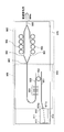
- a light modulation device using such a laser device there is a structure in which a laser device 900 and a ring assist light modulator 960 are combined as shown in FIG.
- the laser device 900 includes an optical semiconductor element 910 called SOA (Semiconductor Optical Amplifier) and a wavelength selective reflection element 950 in which an optical waveguide is formed.
- SOA semiconductor Optical Amplifier
- a gain waveguide 911 is formed in the optical semiconductor element 910, an antireflection film 912 is formed on one surface of the end face of the gain waveguide 911 from which light is emitted, and an end face of the gain waveguide 911 is formed.
- a highly reflective film 913 is formed on the other surface.
- the wavelength selective reflection element 950 includes a first optical waveguide 951, a ring resonator 952, a second optical waveguide 953, and a wavelength selective reflection mirror 954 formed in the second optical waveguide 953.
- the optical semiconductor element 910 and the wavelength selective reflection element 950 include an output end 911a of the gain waveguide 911 on one surface of the optical semiconductor element 910 and an incident end 951a of light in the first optical waveguide 951 of the wavelength selective reflection element 950. And are installed so as to face each other.
- the ring assist optical modulator 960 is provided with a first modulator optical waveguide 961 and a second modulator optical waveguide 962.
- the first modulator optical waveguide 961 and the second modulator optical waveguide 962 are connected by an optical waveguide 965 on the light incident side and an optical waveguide 966 on the light output side.
- a plurality of ring resonators 963 are provided in the vicinity of the side portion of the first modulator optical waveguide 961, and a plurality of ring resonances are provided in the vicinity of the side portion of the second modulator optical waveguide 962.
- a container 964 is provided.
- a resonator is formed by a high reflection film 913 formed on the other surface of the optical semiconductor element 910, a ring resonator 952 and a wavelength selective reflection mirror 954 formed on the wavelength selective reflection element 950. Is done. Therefore, in this laser device 900, light is emitted by passing a current or the like through the optical semiconductor element 910, and the light emitted from the optical semiconductor element 910 is laser-oscillated by a resonator or the like to be emitted from the second optical waveguide 953. The laser beam is emitted from the end 953a.
- the laser light emitted from the wavelength selective reflection element 950 enters the ring assist light modulator 960, propagates through the incident-side optical waveguide 965, and then propagates through the first modulator optical waveguide 961 and the second laser light. Is once branched into a laser beam propagating through the modulator optical waveguide 962.
- the phase of the propagating light can be modulated by applying a voltage to the first modulator optical waveguide 961 or the second modulator optical waveguide 962. Thereafter, the laser light propagating through the first modulator optical waveguide 961 and the laser light propagating through the second modulator optical waveguide 962 are combined in the output-side optical waveguide 966 and output from the output-side optical waveguide 966.
- the light is emitted from the end 966a. Since the laser light emitted from the emission end 966a of the optical waveguide 966 is obtained by coupling and interfering with the phase modulated in the first modulator optical waveguide 961 or the second modulator optical waveguide 962. The light is emitted as modulated signal light whose light intensity is modulated.
- the wavelength selective reflection element 950 and the ring assist light modulator 960 are formed on the same silicon substrate 970.
- the operating wavelength band capable of efficiently performing optical modulation is as narrow as about 1 nm near the resonance wavelength of the ring waveguide. It is required to match the resonance wavelength of the ring of the ring assist light modulator 960.
- the ring resonator 952 in the wavelength selective reflection element 950 and the ring resonators 963 and 964 in the ring assist light modulator 960 are formed to have the same structure.
- the wavelength selective reflection element 950 selects one of the transmission center wavelengths of the ring resonator 952 that periodically exists by the wavelength selective reflection mirror 954, thereby determining the oscillation wavelength of the laser light. .
- the ring resonator 952 and the ring resonators 963 and 964 are formed to have the same period length.
- the transmission wavelengths of the ring resonator 952 and the ring resonators 963 and 964 automatically match, the laser light having the operating wavelength in the ring assist light modulator 960 can be emitted without performing special control.
- the light can be emitted from the laser device 900.
- the wavelength selective reflection element 950 and the ring assist light modulator 960 are formed on the same silicon substrate 970, the operation is hindered even if a temperature change occurs in the silicon substrate 970. Absent.
- the temperature of the silicon substrate 970 rises or falls as a whole, and therefore the wavelength shift occurs similarly in the ring resonator 952 and the ring resonators 963 and 964. Therefore, stable operation can be maintained even when the temperature of the silicon substrate changes.
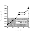
- FIG. 4 shows the relationship between the amount of current for driving the optical semiconductor element 910 obtained based on FIG. 3 and the peak wavelength.
- the driving current of the optical semiconductor element 910 is relatively low, the oscillation wavelength in the laser device 900 is within the operating wavelength band of the ring assist optical modulator 960, so that efficient optical modulation is possible.
- the drive current of the optical semiconductor element 910 is increased, the oscillation wavelength in the laser device 900 is independently shifted to the long wavelength side.
- efficient light modulation cannot be performed. .
- the optical semiconductor element in a laser apparatus having an optical semiconductor element formed of a compound semiconductor material and a wavelength selective reflection element including an optical waveguide, includes a first gain waveguide and , A second gain waveguide, a DBR waveguide formed between the first gain waveguide and the second gain waveguide, and a first current flowing through the first gain waveguide.
- An anti-reflection film is formed on an element end face to which the second gain waveguide is connected, and an electrode and a second electrode for passing a current through the second gain waveguide.
- the optical waveguide in the wavelength selective reflection element reflects light having a predetermined wavelength out of incident light, and the first gain waveguide and the wavelength selective reflector are optically coupled.
- the first gain waveguide as a gain medium, It characterized by having a laser resonator formed by the road and said wavelength selective reflective element.
- a first gain waveguide formed of a compound semiconductor material a second gain waveguide formed of a compound semiconductor material, and the first gain
- a DBR waveguide formed of a compound semiconductor material a first electrode for passing a current through the first gain waveguide, and the second gain guide between the waveguide and the second gain waveguide.
- an end face to which the first gain waveguide is connected and an end face to which the second gain waveguide is connected are both non-reflective.
- a film is formed.
- the disclosed laser device it is possible to increase the intensity of the laser beam without shifting the wavelength.
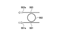
- the first optical waveguide 981 corresponds to the first optical waveguide 951 in the wavelength selective reflection element 950 shown in FIG. 2, and the ring resonator 982 corresponds to the ring resonator 952.
- the second optical waveguide 983 corresponds to the second optical waveguide 953.
- the entrance end, the exit end, and the entrance / exit end of the optical waveguide may be described as the end face of the optical waveguide.
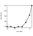
- the shift amount of the peak wavelength rapidly increases above a certain intensity.
- Such a sudden increase in the shift amount of the peak wavelength is considered to be caused by the temperature around the ring resonator 982 rising due to the incident light, and the transmission center wavelength in the ring resonator 982 being shifted. . Therefore, also in the laser apparatus 900 using the wavelength selective reflection element 950 having the same structure as that shown in FIG. 5, the transmission center wavelength of the ring resonator is shifted for the same reason, and the transmission of the ring resonator is performed. It is assumed that the wavelength of the laser light determined by the center wavelength shifts. Therefore, even if the output of the laser beam emitted from the laser device is increased, it is considered that no peak shift occurs if the intensity of the laser beam incident on the wavelength selective reflection element 950 does not increase.
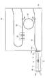
- FIG. 7 shows the structure of the laser device in this embodiment.
- the laser device in the present embodiment has an optical semiconductor element 10 and a wavelength selective reflection element 50.
- the optical semiconductor element 10 includes a gain waveguide made of a compound semiconductor material.
- the optical semiconductor element 10 has a first gain waveguide 11 on one side and a second gain waveguide 12 on the other side.
- a DBR (Distributed Bragg Reflector) waveguide 13 is provided between the first gain waveguide 11 and the second gain waveguide 12.
- An antireflection film 14 is formed on one surface of the optical semiconductor element 10 which is the end surface of the first gain waveguide 11, and light opposite to the one surface which is the end surface of the second gain waveguide 12.
- An antireflection film 15 is formed on the other surface of the semiconductor element 10. Note that the end face of the first gain waveguide 11 becomes the entrance / exit end 11 a of the first gain waveguide 11, and the end face of the second gain waveguide 12 becomes the exit end 12 a of the second gain waveguide 12. Become.
- the wavelength selective reflection element 50 is formed in the first optical waveguide 51, the ring resonator 52, the second optical waveguide 53, and the second optical waveguide 53, and serves as a wavelength selective reflection mirror that reflects only a specific wavelength. And a DBR waveguide 54.
- the first optical waveguide 51, the ring resonator 52, the second optical waveguide 53, and the DBR waveguide 54 are formed on a silicon substrate 70, and are formed by, for example, a silicon optical waveguide surrounded by silicon oxide or the like. Has been.
- the optical waveguides such as the first optical waveguide 51, the ring resonator 52, the second optical waveguide 53, and the DBR waveguide 54 are formed by processing an SOI (Silicon on Insulator) substrate or the like.
- SOI Silicon on Insulator
- a silicon oxide layer in an SOI substrate is used as a lower clad
- an optical waveguide is formed by processing a silicon layer on the silicon oxide layer
- a silicon oxide layer is formed on the formed optical waveguide. It has a structure in which a clad is formed.
- the optical semiconductor element 10 and the wavelength selective reflection element 50 are an incident / exit end 11a of the first gain waveguide 11 in the optical semiconductor element 10 and an incident / exit end of light of the first optical waveguide 51 in the wavelength selective reflection element 50. It is installed so as to face 51a.
- a resonator is formed by the DBR waveguide 13 in the optical semiconductor element 10 and the ring resonator 52 and the DBR waveguide 54 in the wavelength selective reflection element 50.
- light is emitted by passing a current through a region where the first gain waveguide 11 of the optical semiconductor element 10 is formed, and the emitted light is laser-oscillated using a resonator. And is amplified in the second gain waveguide 12. Thereby, the light amplified in the second gain waveguide 12 can be emitted as laser light from the emission end 12 a of the second gain waveguide 12 of the optical semiconductor element 10.
- laser light having a resonance wavelength is oscillated in the first gain waveguide 11 and the resonator, and the laser light oscillated in the second gain waveguide 12 is amplified.
- the functions of oscillation and amplification are separated. Therefore, even if the amount of current flowing through the first gain waveguide 11 is fixed, the intensity of the laser light can be increased by increasing the amount of current flowing through the second gain waveguide 12.
- the optical semiconductor can be obtained even if the current amount of the second gain waveguide 12 is changed to increase the intensity of the laser beam emitted from the emission end 12a. Since the intensity of light incident on the wavelength selective reflection element 50 from the element 10 is constant, the transmission center wavelength of the ring resonator inside the wavelength selective reflection element 50 does not shift, and the laser oscillation wavelength does not shift. Therefore, in the laser device according to the present embodiment, even if the intensity of the laser beam emitted from the emission end 12a of the second gain waveguide 12 is increased, the oscillation wavelength does not shift.
- a desired constant wavelength laser beam is emitted from the emission end 12a of the second gain waveguide 12 without depending on the intensity of the emitted laser beam. Can do. Furthermore, if the amount of current flowing through the gain waveguide 1 is fixed to a relatively small value, the light intensity inside the ring resonator decreases, so there is no shift of the transmission center wavelength due to heat generation due to light incidence, and the ring resonator It becomes possible to maintain the original transmission center wavelength.
- FIGS. 9A is a cross-sectional view taken along the alternate long and short dash line 8A-8B in FIG. 8, and FIG. 9B is a cross-sectional view taken along the alternate long and short dash line 8C-8D in FIG.
- FIG. 9C is a cross-sectional view taken along one-dot chain line 8E-8F in FIG.
- the optical semiconductor element 10 has the first gain waveguide 11 formed on one side and the second gain waveguide 12 formed on the other side.
- a DBR waveguide 13 is formed between the first gain waveguide 11 and the second gain waveguide 12.
- the optical semiconductor element 10 is formed on the n-InP substrate 20 by epitaxially growing a semiconductor layer formed of a compound semiconductor material by MOCVD (Metal Organic Chemical Vapor Deposition) or the like.
- MOCVD Metal Organic Chemical Vapor Deposition
- a p-InGaAs / p-InGaAsP contact layer for reducing the contact resistance with the electrode may be placed on the p-InP cladding layer.
- the MQW active layer 22 thus formed forms the first gain waveguide 11 and the second gain waveguide 12.
- the MQW active layer 22 is formed by alternately stacking i-InGaAsP having different compositions, and is formed to have a thickness of 100 nm and a PL (Photoluminescence) wavelength of 1.55 ⁇ m.
- a PL Photoluminescence
- an n-InP clad layer 21, an optical waveguide core layer 24, and a p-InP clad layer 23 are stacked on the n-InP substrate 20.
- the DBR waveguide 13 is formed by the optical waveguide core layer 24 thus formed.
- the optical waveguide core layer 24 is formed of i-InGaAsP having a thickness of 200 nm and a PL wavelength of 1.30 ⁇ m.
- a diffraction grating 25 is formed of n-InGaAsP. The coupling coefficient and period of the diffraction grating are adjusted so as to select one of the resonant wavelengths generated periodically in the ring waveguide inside the wavelength selective reflection element 50 at a wavelength near 1.55 ⁇ m.
- the first gain waveguide 11, the second gain waveguide 12, and the DBR waveguide 13 have a mesa structure with a width of 1.5 ⁇ m, and both sides of the mesa structure have high resistance doped with Fe as an impurity element.
- the SI-InP layer 29 is formed. Note that the first gain waveguide 11, the second gain waveguide 12, and the DBR waveguide 13 of the optical semiconductor element 10 according to the present embodiment are identical in n-type by using a bad joint growth technique by MOCVD. It can be formed on the InP substrate 20
- the formed first gain waveguide 11 has a length of about 400 ⁇ m
- the second gain waveguide 12 has a length of about 600 ⁇ m
- the DBR waveguide 13 has a length of about 600 ⁇ m.
- the coupling coefficient ⁇ in the DBR waveguide 13 is formed to be 100 cm ⁇ 1, and the reflectance in the DBR waveguide 13 is about 60%.
- a lower electrode 26 serving as a common electrode is formed on the back surface of the n-InP substrate 20 in a region where the first gain waveguide 11, the second gain waveguide 12, and the DBR waveguide 13 are formed.
- a first upper electrode 27 is formed on the p-InP cladding layer 23 in the region where the first gain waveguide 11 is formed, and the region where the second gain waveguide 12 is formed.
- a second upper electrode 28 is formed on the p-InP cladding layer 23 in FIG. In this way, the first upper electrode 27 is formed in the region where the first gain waveguide 11 is formed, and the second upper electrode 28 is formed in the region where the second gain waveguide 12 is formed. Different currents can be injected independently between the first gain waveguide 11 and the second gain waveguide 12.
- the first upper electrode 27 and the second upper electrode 28 are made of Ti / Pt / Au.
- the first gain waveguide 11 and the second gain waveguide 12 are in the vicinity of one surface of the optical semiconductor element 10 and the normal of the other surface in the vicinity of the end face.
- each is formed so as to be inclined by about 7 °.
- the wavelength selective reflection element 50 is formed using an SOI substrate in which a silicon oxide layer and a silicon layer are sequentially laminated on a silicon substrate 70.
- This SOI substrate is formed by sequentially laminating a silicon oxide layer having a thickness of about 3 ⁇ m and a silicon layer having a thickness of about 300 nm on a silicon substrate.
- the wavelength selective reflection element 50 is formed by applying a photoresist on a silicon layer of an SOI substrate and performing exposure and development with an exposure apparatus to form a resist pattern (not shown). This resist pattern is formed on a region where the first optical waveguide 51, the ring resonator 52, the second optical waveguide 53, and the wavelength selective reflection mirror 54 are formed.
- the first optical waveguide 51, the ring resonator 52, the second optical waveguide 53, and the optical waveguide that becomes the wavelength selective reflection mirror 54 are formed of silicon.
- the first optical waveguide 51, the ring resonator 52, the second optical waveguide 53, and the optical waveguide serving as the DBR waveguide 54 are formed by rib waveguides.
- a slab region having a thickness of about 50 nm is formed around a core region having a width of about 500 nm and a thickness of about 300 ⁇ m.
- an upper clad is formed by forming a silicon oxide layer having a thickness of about 2 ⁇ m on the optical waveguide made of silicon. Thereby, the wavelength selective reflection element 50 can be formed.
- the first optical waveguide 51, the ring resonator 52, the second optical waveguide 53, and the DBR waveguide 54 are not only rib cores but also slab regions, and only the core region.
- a so-called channel waveguide having a formed structure may be used.
- the ring resonator 52 is formed so as to have a radius of 8 ⁇ m.
- the gap G1 between the first optical waveguide 51 and the ring resonator 52 and the second optical waveguide 53 and the ring resonance are formed.
- the gap G2 with the vessel 52 is formed to be about 300 nm.
- the DBR waveguide 54 is formed by forming a side diffraction grating having a length of about 3 ⁇ m and a pitch of about 300 nm on the side wall of the optical waveguide in the region where the length of the second optical waveguide 53 is about 500 ⁇ m. Has been.
- the reflection wavelength band of the DBR waveguide 54 is made to coincide with the reflection wavelength band of the DBR waveguide of the optical semiconductor element 10 so that the same wavelength among the periodic transmission wavelengths of the ring resonator is reflected.
- the wavelength selective reflection element 50 is formed so that the end surfaces of the first optical waveguide 51 and the second optical waveguide 53 are inclined by about 15 ° with respect to the normal line of the end surface. Furthermore, it is formed so as to have a tapered shape in which the width of the tip portion becomes narrow.
- the input / output end 11a of the first gain waveguide 11 in the optical semiconductor element 10 and the input / output end 51a of the first optical waveguide 51 in the wavelength selective reflection element 50 are aligned.
- the optical semiconductor element 10 and the wavelength selective reflection element 50 are fixed.
- the optical semiconductor element 10 and the wavelength selective reflection element 50 are embedded with a refractive index matching resin material (not shown) between the aligned optical semiconductor element 10 and the wavelength selective reflection element 50. It is fixed by.
- the laser device in this embodiment can be manufactured.
- laser light having a resonance wavelength is oscillated in the first gain waveguide 11 and the resonator, and the laser light oscillated in the second gain waveguide 12 is amplified.
- the functions of light oscillation and amplification are separated. Therefore, by fixing the amount of current flowing through the first gain waveguide 11 and increasing the amount of current flowing through the second gain waveguide 12, the laser emitted without causing a shift in the oscillation wavelength of the laser It becomes possible to increase the intensity of light.
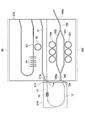
- the present embodiment is a light modulation device, and as shown in FIG. 10, a ring assist light modulator is provided on the end face side of the optical semiconductor element 12a from which the laser light in the laser device in the first embodiment is emitted. 160 is provided. Specifically, the wavelength selective reflection element 50 and the ring assist light modulator 160 are formed on the same silicon substrate 170. In the silicon substrate 170, the wavelength selective reflection element 50, the ring assist light modulator 160, A groove 171 is formed between them. In the present embodiment, the optical semiconductor element 10 in the first embodiment is installed in the groove portion 171.
- the optical semiconductor element 10 and the wavelength selective reflection element 50 are the input / output end 11 a of the first gain waveguide 11 of the optical semiconductor element 10 and the first optical waveguide 51 of the wavelength selective reflection element 50. Is aligned with the incident / exit end 51a.
- the optical semiconductor element 10 and the ring assist optical modulator 160 include an emission end 12a of the second gain waveguide 12 of the optical semiconductor element 10 and an incident end 165a of the optical waveguide 165 in the ring assist optical modulator 160. Alignment has been made. As described above, the optical semiconductor element 10 is installed on the silicon substrate 170 in a state where the wavelength selective reflection element 50 and the ring assist light modulator 160 are aligned.
- the ring assist light modulator 160 has a first modulation optical waveguide 161 and a second modulation optical waveguide 162.
- the first modulation optical waveguide 161 and the second modulation optical waveguide 162 are connected by an optical waveguide 165 on the light incident side, and are connected by an optical waveguide 166 on the light emission side.
- a plurality of ring resonators 163 are provided in the vicinity of the side portion of the first modulation optical waveguide 161, and a plurality of ring resonators 164 are provided in the vicinity of the side portion of the second modulation optical waveguide 162. Is provided.
- the laser light emitted from the emission end 12 a of the second gain waveguide 12 of the optical semiconductor element 10 enters from the incident end 165 a of the optical waveguide 165 in the ring assist light modulator 160 and propagates through the optical waveguide 165. Thereafter, the laser beam is branched into a laser beam propagating through the first modulation optical waveguide 161 and a laser beam propagating through the second modulation optical waveguide 162.
- the ring assist light modulator 160 by applying a voltage to the first modulation optical waveguide 161 or the second modulation optical waveguide 162, the phase of the laser light propagating to each can be modulated.
- the laser light propagating through the first modulation optical waveguide 161 and the laser light propagating through the second modulation optical waveguide 162 are combined in the optical waveguide 166 and emitted from the emission end 166 a of the optical waveguide 166.
- the laser light emitted from the emission end 166a of the optical waveguide 166 is obtained by combining those modulated in phase in the first modulation optical waveguide 161 or the second modulation optical waveguide 162, 2 Depending on the phase difference between the two modulation optical waveguides 161 and 162, the light is emitted as modulated signal light whose light intensity is modulated.
- the ring resonator 52 in the wavelength selective reflection element 50 and the ring resonator 163 and the ring resonator 164 in the ring assist light modulator 160 are formed to have the same shape. By forming them in the same shape as described above, the resonance wavelength of the ring resonator 52 in the wavelength selective reflection element 50 and the operating wavelength in the ring assist light modulator 160 can be made coincident with each other without being affected by a temperature change or the like.
- the oscillation wavelength of the laser can be matched with the operating wavelength of the modulator.
- the current value of the first gain waveguide 11a of the semiconductor element 10 is fixed at a relatively low value, and the current value of the second gain waveguide is increased, thereby increasing the semiconductor value. Even when the optical output on the 12a end face side of the element 10 is increased, it is possible to suppress the shift of the transmission center wavelength of the ring resonator 52 of the wavelength selective reflection element 50 so that the laser oscillation wavelength does not change. It becomes. As a result, the operating wavelength of the modulator does not deviate from the oscillation wavelength of the laser, and the laser light intensity can be increased.
- the first modulator optical waveguide 161, the second modulator optical waveguide 162, the optical waveguides 165 and 166, and the plurality of ring resonators 163 and 164 in the ring assist optical modulator 160 are the first modulator optical waveguide 161 in the wavelength selective reflection element 50. It is formed with the same structure as the one optical waveguide 51 and the like. Accordingly, the first modulator optical waveguide 161, the second modulator optical waveguide 162, the optical waveguides 165 and 166, and the plurality of ring resonators 163 and 164 in the ring assist optical modulator 160 are included in the first wavelength selective reflection element 50. 1 optical waveguide 51 and the like can be formed simultaneously.
- the optical semiconductor element 10 is installed on the silicon substrate 170 so that the upper surface of the optical waveguide such as the first optical waveguide 51 is on the upper side.
- a flip chip mounting structure may be used so as to be on the lower side.
- the position of the optical waveguide can be precisely controlled by the thickness of the epitaxial growth from the core portion to the upper clad portion of the optical waveguide. Optical coupling with the optical semiconductor element 10 becomes possible.
- the present embodiment is an optical modulation device, and as shown in FIG. 11, an input / output end 11 a of the first gain waveguide 11 and an output end 12 a of the second gain waveguide 12 in the optical semiconductor element 210 are provided. Both are provided on one surface side of the same optical semiconductor element 210. Therefore, in the present embodiment, as shown in FIG. 11, the second gain waveguide 12 is formed in a curved shape and has a U shape. In the present embodiment, an antireflection film 214 is formed on one surface of the optical semiconductor element 210.
- the wavelength selective reflection element 50 and the ring assist light modulator 160 are formed on the same silicon substrate 270. Therefore, the incident / exit end 51a of the first optical waveguide 51 of the wavelength selective reflection element 50 and the incident end 165a of the optical waveguide 165 in the ring assist optical modulator 160 are formed on the same side surface in the silicon substrate 270. ing.
- the wavelength selective reflection element 50 and the ring assist light modulator 160 are formed on the same surface side with respect to the optical semiconductor element 210, it is not necessary to form a groove or the like, and the light modulation device can be downsized. Can do. Furthermore, since the ring resonator 52 and the ring resonators 163 and 164 can be formed at closer positions, the influence of wavelength shift due to temperature change can be further reduced.
- this embodiment may have a structure in which light is folded inside the optical semiconductor element by disposing a reflective 2 ⁇ 2 multimode interference waveguide near the end face of the optical semiconductor element. In this case, since it is not necessary to bend the second gain waveguide 12, the optical semiconductor element 210 can be further reduced in size.
- the present embodiment is a laser device, and as shown in FIG. 12, the wavelength selective reflection element 350 is not provided with the DBR waveguide 54 as in the first embodiment, but has a wavelength dependency.
- This is a structure provided with a loop mirror 355 having a very small amount.
- the loop mirror 355 has a feature that a reflection mirror having a high reflectance can be formed regardless of the wavelength by forming a loop-shaped optical waveguide without forming an end face or the like. It is promising as a reflecting mirror applied to an element using a silicon waveguide that is expected to be integrated with density. Therefore, in the laser device according to the present embodiment, among the periodic transmission wavelengths in the ring resonator 52 of the wavelength selective reflection element 350, the wavelength selected in the DBR waveguide 13 of the semiconductor element 10 becomes the resonance wavelength.
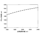
- FIG. 13 shows the relationship between the optical waveguide width and the Bragg wavelength in the DBR waveguide 54 formed of silicon in the wavelength selective reflection element 50 according to the first embodiment or the like.
- FIG. 14 shows the relationship between the optical waveguide width and the Bragg wavelength in the DBR waveguide 13 formed of a compound semiconductor in the optical semiconductor element 10. As shown in FIGS. 13 and 14, the dependence of the Bragg wavelength on the width of the optical waveguide is shown in FIG. 14 for the DBR waveguide 54 formed in the wavelength selective reflection element 50 shown in FIG. It is larger than the DBR waveguide 13 formed in the optical semiconductor element 10. That is, the dependence of the optical waveguide width on the Bragg wavelength is such that the DBR waveguide 54 formed in the wavelength selective reflection element 50 shown in FIG.
- the DBR waveguide 13 has the DBR formed in the optical semiconductor element 10 shown in FIG. It is larger than the waveguide 13. For this reason, in the DBR waveguide 54 and the like, when the width of the optical waveguide is formed differently due to a manufacturing error or the like, the selected wavelength may be largely shifted from the desired wavelength. However, in the present embodiment, the function of selecting one of the resonance wavelengths of the ring resonator is provided in the DBR waveguide 13 of the semiconductor element 10, not in the loop mirror 355 inside the wavelength selective reflection element 350. Thus, the resonance wavelength can be more precisely set to a desired value, so that the uniformity of the oscillation wavelength of the laser beam can be further improved.
- the laser device in the present embodiment can be used in the light modulation devices in the second and third embodiments in the same manner as the laser device in the first embodiment.
- optical semiconductor element 11 first gain waveguide 11a input / output end 12 second gain waveguide 12a output end 13 DBR waveguide 14 antireflection film 15 antireflection film 20 n-InP substrate 21 n-InP clad layer 22 MQW Active layer 23 p-InP cladding layer 24 Optical waveguide core layer 25 Diffraction grating 26 Lower electrode 27 First upper electrode 28 Second upper electrode 29 SI-InP layer 50 Wavelength selective reflection element 51 First optical waveguide 51a Incoming and outgoing End 52 Ring resonator 53 Third optical waveguide 54 Wavelength selective reflector (DBR waveguide) 70 Silicon substrate 160 Ring assist optical modulator 161 First modulator optical waveguide 162 Second modulator optical waveguide 163 Ring resonator 164 Ring resonator 165 Optical waveguide 165a Incoming end 166 Optical waveguide 166a Outgoing end 170 Silicon substrate
Landscapes
- Physics & Mathematics (AREA)
- Electromagnetism (AREA)
- Optics & Photonics (AREA)
- General Physics & Mathematics (AREA)
- Condensed Matter Physics & Semiconductors (AREA)
- Engineering & Computer Science (AREA)
- Plasma & Fusion (AREA)
- Microelectronics & Electronic Packaging (AREA)
- Semiconductor Lasers (AREA)
- Optical Integrated Circuits (AREA)
- Optical Modulation, Optical Deflection, Nonlinear Optics, Optical Demodulation, Optical Logic Elements (AREA)
- Optical Couplings Of Light Guides (AREA)
Abstract
La présente invention concerne un dispositif laser comportant un élément semi-conducteur optique formé d'un matériau à base de composé semi-conducteur et comportant un élément réfléchissant à sélection de longueur d'onde qui comprend un guide d'ondes optique, caractérisé en ce que l'élément semi-conducteur optique possède un premier guide d'ondes à gain, un second guide d'ondes à gain, un guide d'ondes à DBR formé entre le premier guide d'ondes à gain et le second guide d'ondes à gain, une première électrode permettant le passage d'un courant électrique à travers le premier guide d'ondes à gain, et une seconde électrode permettant le passage d'un courant électrique à travers le second guide d'ondes, un film antireflet étant formé sur la surface d'extrémité de l'élément connectée au second guide d'ondes à gain, le guide d'ondes optique de l'élément réfléchissant à sélection de longueur d'onde réfléchissant une lumière de longueur d'onde donnée en tant que partie de lumière incidente, le premier guide d'ondes à gain et l'élément réfléchissant à sélection de longueur d'onde étant couplés optiquement, le premier guide d'ondes à gain constituant un milieu de gain, et un résonateur laser étant formé par le guide d'ondes à DBR et par l'élément réfléchissant à sélection de longueur d'onde.
Priority Applications (4)
| Application Number | Priority Date | Filing Date | Title |
|---|---|---|---|
| PCT/JP2013/051761 WO2014115330A1 (fr) | 2013-01-28 | 2013-01-28 | Dispositif laser, dispositif de modulation optique et élément semi-conducteur optique |
| CN201380070494.4A CN104937791B (zh) | 2013-01-28 | 2013-01-28 | 激光装置、光调制装置以及光半导体元件 |
| JP2014558408A JP6020601B2 (ja) | 2013-01-28 | 2013-01-28 | レーザ装置、光変調装置及び光半導体素子 |
| US14/747,651 US9312663B2 (en) | 2013-01-28 | 2015-06-23 | Laser device, light modulation device, and optical semiconductor device |
Applications Claiming Priority (1)
| Application Number | Priority Date | Filing Date | Title |
|---|---|---|---|
| PCT/JP2013/051761 WO2014115330A1 (fr) | 2013-01-28 | 2013-01-28 | Dispositif laser, dispositif de modulation optique et élément semi-conducteur optique |
Related Child Applications (1)
| Application Number | Title | Priority Date | Filing Date |
|---|---|---|---|
| US14/747,651 Continuation US9312663B2 (en) | 2013-01-28 | 2015-06-23 | Laser device, light modulation device, and optical semiconductor device |
Publications (1)
| Publication Number | Publication Date |
|---|---|
| WO2014115330A1 true WO2014115330A1 (fr) | 2014-07-31 |
Family
ID=51227143
Family Applications (1)
| Application Number | Title | Priority Date | Filing Date |
|---|---|---|---|
| PCT/JP2013/051761 Ceased WO2014115330A1 (fr) | 2013-01-28 | 2013-01-28 | Dispositif laser, dispositif de modulation optique et élément semi-conducteur optique |
Country Status (4)
| Country | Link |
|---|---|
| US (1) | US9312663B2 (fr) |
| JP (1) | JP6020601B2 (fr) |
| CN (1) | CN104937791B (fr) |
| WO (1) | WO2014115330A1 (fr) |
Cited By (8)
| Publication number | Priority date | Publication date | Assignee | Title |
|---|---|---|---|---|
| JP2016102926A (ja) * | 2014-11-28 | 2016-06-02 | 富士通株式会社 | 波長可変レーザ及び波長可変レーザモジュール |
| JP2016213379A (ja) * | 2015-05-12 | 2016-12-15 | 富士通株式会社 | 多波長レーザ光源及び波長多重通信システム |
| JP2017003670A (ja) * | 2015-06-05 | 2017-01-05 | 日本電信電話株式会社 | ハイブリッド集積型光送信器 |
| JP2018532277A (ja) * | 2015-10-28 | 2018-11-01 | ロックリー フォトニクス リミテッドRockley Photonics Limited | 離散波長可変レーザ |
| EP3358684A4 (fr) * | 2015-09-29 | 2019-08-21 | Nippon Telegraph and Telephone Corporation | Dispositif laser à semi-conducteur |
| JP2021150309A (ja) * | 2020-03-16 | 2021-09-27 | 株式会社デンソー | レーザ光源 |
| JPWO2022137330A1 (fr) * | 2020-12-22 | 2022-06-30 | ||
| JP2022129390A (ja) * | 2021-02-24 | 2022-09-05 | 浜松ホトニクス株式会社 | 外部共振型レーザモジュール |
Families Citing this family (11)
| Publication number | Priority date | Publication date | Assignee | Title |
|---|---|---|---|---|
| US9739940B2 (en) * | 2015-03-12 | 2017-08-22 | Medlumics S.L. | Bidirectional photonic integrated circuit with suppressed reflection |
| FR3046850B1 (fr) * | 2016-01-15 | 2018-01-26 | Universite De Strasbourg | Guide optique ameliore et systeme optique comportant un tel guide optique |
| US9608406B1 (en) * | 2016-01-22 | 2017-03-28 | Oracle International Corporation | Wavelength control of a dual-ring laser |
| JPWO2017138649A1 (ja) * | 2016-02-12 | 2018-12-13 | 古河電気工業株式会社 | レーザモジュール |
| US20180006433A1 (en) * | 2016-06-29 | 2018-01-04 | Mellanox Technologies Silicon Photonics Inc. | Laser chip with multiple outputs on common side |
| JP7039948B2 (ja) | 2017-11-17 | 2022-03-23 | 株式会社デンソー | 測距センサ |
| CN107887785B (zh) * | 2017-12-04 | 2020-06-16 | 电子科技大学 | 一种光纤与波导谐振环复合的单频光纤激光器 |
| EP3764489A4 (fr) * | 2018-04-09 | 2021-03-24 | Huawei Technologies Co., Ltd. | Laser à longueur d'onde accordable |
| TWI712274B (zh) * | 2019-09-12 | 2020-12-01 | 源傑科技股份有限公司 | 電光調制裝置 |
| JP7259699B2 (ja) * | 2019-10-29 | 2023-04-18 | 住友電気工業株式会社 | 半導体光素子 |
| WO2025019813A1 (fr) * | 2023-07-20 | 2025-01-23 | University Of Southern California | Guide d'ondes de génération de faisceau de troie utilisant des points de lagrange |
Citations (5)
| Publication number | Priority date | Publication date | Assignee | Title |
|---|---|---|---|---|
| JP2003508927A (ja) * | 1999-08-31 | 2003-03-04 | コーニング・インコーポレーテッド | 一体化された変調器を有する波長固定外部共振器レーザ |
| JP2003174223A (ja) * | 2001-09-28 | 2003-06-20 | Furukawa Electric Co Ltd:The | 半導体レーザ装置、半導体レーザモジュールおよび半導体レーザ制御方法 |
| JP2010027664A (ja) * | 2008-07-15 | 2010-02-04 | Fujitsu Ltd | 光半導体装置 |
| JP2010239007A (ja) * | 2009-03-31 | 2010-10-21 | Opnext Japan Inc | 半導体レーザ素子 |
| JP2011253930A (ja) * | 2010-06-02 | 2011-12-15 | Fujitsu Ltd | 半導体光装置 |
Family Cites Families (7)
| Publication number | Priority date | Publication date | Assignee | Title |
|---|---|---|---|---|
| US6704338B2 (en) * | 2001-09-28 | 2004-03-09 | Furukawa Electric Co., Ltd. | Semiconductor laser device, semiconductor laser module, and semiconductor laser control method |
| JP4378936B2 (ja) * | 2002-11-06 | 2009-12-09 | 住友電気工業株式会社 | 半導体レーザ |
| JP5233090B2 (ja) * | 2006-07-28 | 2013-07-10 | 沖電気工業株式会社 | キャリア抑圧光パルス列発生方法及びこの方法を実現するモード同期半導体レーザ |
| US20090092159A1 (en) | 2007-05-28 | 2009-04-09 | Sumitomo Electric Industries, Ltd. | Semiconductor light-emitting device with tunable emission wavelength |
| JP2009059729A (ja) | 2007-08-29 | 2009-03-19 | Sumitomo Electric Ind Ltd | 半導体発光素子 |
| KR100987793B1 (ko) * | 2008-10-10 | 2010-10-13 | 한국전자통신연구원 | 반사형 반도체 광 증폭기 및 이를 이용하는 광신호 처리방법 |
| US8737446B2 (en) * | 2010-03-25 | 2014-05-27 | Sumitomo Electric Industries, Ltd. | Semiconductor laser |
-
2013
- 2013-01-28 WO PCT/JP2013/051761 patent/WO2014115330A1/fr not_active Ceased
- 2013-01-28 JP JP2014558408A patent/JP6020601B2/ja active Active
- 2013-01-28 CN CN201380070494.4A patent/CN104937791B/zh not_active Expired - Fee Related
-
2015
- 2015-06-23 US US14/747,651 patent/US9312663B2/en active Active
Patent Citations (5)
| Publication number | Priority date | Publication date | Assignee | Title |
|---|---|---|---|---|
| JP2003508927A (ja) * | 1999-08-31 | 2003-03-04 | コーニング・インコーポレーテッド | 一体化された変調器を有する波長固定外部共振器レーザ |
| JP2003174223A (ja) * | 2001-09-28 | 2003-06-20 | Furukawa Electric Co Ltd:The | 半導体レーザ装置、半導体レーザモジュールおよび半導体レーザ制御方法 |
| JP2010027664A (ja) * | 2008-07-15 | 2010-02-04 | Fujitsu Ltd | 光半導体装置 |
| JP2010239007A (ja) * | 2009-03-31 | 2010-10-21 | Opnext Japan Inc | 半導体レーザ素子 |
| JP2011253930A (ja) * | 2010-06-02 | 2011-12-15 | Fujitsu Ltd | 半導体光装置 |
Cited By (15)
| Publication number | Priority date | Publication date | Assignee | Title |
|---|---|---|---|---|
| US9722397B2 (en) | 2014-11-28 | 2017-08-01 | Fujitsu Limited | Tunable laser and tunable laser module |
| JP2016102926A (ja) * | 2014-11-28 | 2016-06-02 | 富士通株式会社 | 波長可変レーザ及び波長可変レーザモジュール |
| JP2016213379A (ja) * | 2015-05-12 | 2016-12-15 | 富士通株式会社 | 多波長レーザ光源及び波長多重通信システム |
| JP2017003670A (ja) * | 2015-06-05 | 2017-01-05 | 日本電信電話株式会社 | ハイブリッド集積型光送信器 |
| EP3358684A4 (fr) * | 2015-09-29 | 2019-08-21 | Nippon Telegraph and Telephone Corporation | Dispositif laser à semi-conducteur |
| JP7108538B2 (ja) | 2015-10-28 | 2022-07-28 | ロックリー フォトニクス リミテッド | マルチセクションデジタルスーパーモード分布ブラッグ反射器及び離散波長可変レーザ |
| JP2018532277A (ja) * | 2015-10-28 | 2018-11-01 | ロックリー フォトニクス リミテッドRockley Photonics Limited | 離散波長可変レーザ |
| JP2021150309A (ja) * | 2020-03-16 | 2021-09-27 | 株式会社デンソー | レーザ光源 |
| JP7437682B2 (ja) | 2020-03-16 | 2024-02-26 | 株式会社デンソー | レーザ光源 |
| JPWO2022137330A1 (fr) * | 2020-12-22 | 2022-06-30 | ||
| JP7586194B2 (ja) | 2020-12-22 | 2024-11-19 | 日本電信電話株式会社 | 波長可変レーザ |
| JP2022129390A (ja) * | 2021-02-24 | 2022-09-05 | 浜松ホトニクス株式会社 | 外部共振型レーザモジュール |
| US20220337033A1 (en) * | 2021-02-24 | 2022-10-20 | Hamamatsu Photonics K.K. | External resonance-type laser module |
| JP7758599B2 (ja) | 2021-02-24 | 2025-10-22 | 浜松ホトニクス株式会社 | 外部共振型レーザモジュール |
| US12525768B2 (en) * | 2021-02-24 | 2026-01-13 | Hamamatsu Photonics K.K. | External resonance-type laser module |
Also Published As
| Publication number | Publication date |
|---|---|
| JP6020601B2 (ja) | 2016-11-02 |
| US20150288148A1 (en) | 2015-10-08 |
| CN104937791B (zh) | 2017-09-22 |
| JPWO2014115330A1 (ja) | 2017-01-26 |
| CN104937791A (zh) | 2015-09-23 |
| US9312663B2 (en) | 2016-04-12 |
Similar Documents
| Publication | Publication Date | Title |
|---|---|---|
| JP6020601B2 (ja) | レーザ装置、光変調装置及び光半導体素子 | |
| Tran et al. | Ring-resonator based widely-tunable narrow-linewidth Si/InP integrated lasers | |
| CN107431331B (zh) | 波长可变激光元件以及激光模块 | |
| US10680410B2 (en) | External cavity laser | |
| JP5811273B2 (ja) | 光素子、光送信素子、光受信素子、ハイブリッドレーザ、光送信装置 | |
| EP2866067B1 (fr) | Coupleur optique à base de réseau | |
| EP3072188B1 (fr) | Cavité laser à miroir à boucle de sagnac sur plate-forme photonique au silicium | |
| US9130350B2 (en) | Laser device that includes ring resonator | |
| JP5764875B2 (ja) | 半導体光装置 | |
| US9020006B2 (en) | High density laser optics | |
| US9995876B2 (en) | Configurable compact photonic platforms | |
| WO2013021421A1 (fr) | Élément optique à semi-conducteurs | |
| US8576472B2 (en) | Optoelectronic device with controlled temperature dependence of the emission wavelength and method of making same | |
| US7995625B2 (en) | Resonator of hybrid laser diode | |
| JP6247944B2 (ja) | 水平共振器面出射型レーザ素子 | |
| CN111699597B (zh) | 反射滤波器元件以及波长可变激光元件 | |
| WO2016152274A1 (fr) | Élément laser à longueur d'onde variable et module laser | |
| JP2017187690A (ja) | 光素子、光モジュール及び光伝送システム | |
| US20250055254A1 (en) | Semiconductor Laser | |
| JP5034572B2 (ja) | 光源装置 | |
| Lamponi | Hybrid III-V on silicon lasers for telecommunication applications | |
| CN103748748B (zh) | 光半导体元件 | |
| JP2024079265A (ja) | 波長可変レーザ素子およびその製造方法 | |
| Bakir et al. | Group III–V on Silicon: A Brand-New Optoelectronics | |
| CN103748748A (zh) | 光半导体元件 |
Legal Events
| Date | Code | Title | Description |
|---|---|---|---|
| 121 | Ep: the epo has been informed by wipo that ep was designated in this application |
Ref document number: 13872978 Country of ref document: EP Kind code of ref document: A1 |
|
| ENP | Entry into the national phase |
Ref document number: 2014558408 Country of ref document: JP Kind code of ref document: A |
|
| NENP | Non-entry into the national phase |
Ref country code: DE |
|
| 122 | Ep: pct application non-entry in european phase |
Ref document number: 13872978 Country of ref document: EP Kind code of ref document: A1 |