WO2014129507A1 - 検出器、pet装置及びx線ct装置 - Google Patents
検出器、pet装置及びx線ct装置 Download PDFInfo
- Publication number
- WO2014129507A1 WO2014129507A1 PCT/JP2014/053941 JP2014053941W WO2014129507A1 WO 2014129507 A1 WO2014129507 A1 WO 2014129507A1 JP 2014053941 W JP2014053941 W JP 2014053941W WO 2014129507 A1 WO2014129507 A1 WO 2014129507A1
- Authority
- WO
- WIPO (PCT)
- Prior art keywords
- electrode
- semiconductor region
- wiring
- semiconductor
- insulating layer
- Prior art date
- Legal status (The legal status is an assumption and is not a legal conclusion. Google has not performed a legal analysis and makes no representation as to the accuracy of the status listed.)
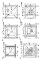
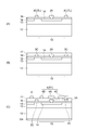
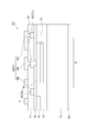
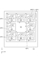
- Ceased
Links
Images



























Classifications
-
- H—ELECTRICITY
- H10—SEMICONDUCTOR DEVICES; ELECTRIC SOLID-STATE DEVICES NOT OTHERWISE PROVIDED FOR
- H10F—INORGANIC SEMICONDUCTOR DEVICES SENSITIVE TO INFRARED RADIATION, LIGHT, ELECTROMAGNETIC RADIATION OF SHORTER WAVELENGTH OR CORPUSCULAR RADIATION
- H10F39/00—Integrated devices, or assemblies of multiple devices, comprising at least one element covered by group H10F30/00, e.g. radiation detectors comprising photodiode arrays
- H10F39/10—Integrated devices
- H10F39/12—Image sensors
- H10F39/18—Complementary metal-oxide-semiconductor [CMOS] image sensors; Photodiode array image sensors
- H10F39/189—X-ray, gamma-ray or corpuscular radiation imagers
- H10F39/1898—Indirect radiation image sensors, e.g. using luminescent members
-
- G—PHYSICS
- G01—MEASURING; TESTING
- G01N—INVESTIGATING OR ANALYSING MATERIALS BY DETERMINING THEIR CHEMICAL OR PHYSICAL PROPERTIES
- G01N23/00—Investigating or analysing materials by the use of wave or particle radiation, e.g. X-rays or neutrons, not covered by groups G01N3/00 – G01N17/00, G01N21/00 or G01N22/00
- G01N23/02—Investigating or analysing materials by the use of wave or particle radiation, e.g. X-rays or neutrons, not covered by groups G01N3/00 – G01N17/00, G01N21/00 or G01N22/00 by transmitting the radiation through the material
- G01N23/04—Investigating or analysing materials by the use of wave or particle radiation, e.g. X-rays or neutrons, not covered by groups G01N3/00 – G01N17/00, G01N21/00 or G01N22/00 by transmitting the radiation through the material and forming images of the material
- G01N23/046—Investigating or analysing materials by the use of wave or particle radiation, e.g. X-rays or neutrons, not covered by groups G01N3/00 – G01N17/00, G01N21/00 or G01N22/00 by transmitting the radiation through the material and forming images of the material using tomography, e.g. computed tomography [CT]
-
- G—PHYSICS
- G01—MEASURING; TESTING
- G01T—MEASUREMENT OF NUCLEAR OR X-RADIATION
- G01T1/00—Measuring X-radiation, gamma radiation, corpuscular radiation, or cosmic radiation
- G01T1/16—Measuring radiation intensity
- G01T1/24—Measuring radiation intensity with semiconductor detectors
- G01T1/241—Electrode arrangements, e.g. continuous or parallel strips or the like
-
- G—PHYSICS
- G01—MEASURING; TESTING
- G01T—MEASUREMENT OF NUCLEAR OR X-RADIATION
- G01T1/00—Measuring X-radiation, gamma radiation, corpuscular radiation, or cosmic radiation
- G01T1/29—Measurement performed on radiation beams, e.g. position or section of the beam; Measurement of spatial distribution of radiation
- G01T1/2914—Measurement of spatial distribution of radiation
- G01T1/2985—In depth localisation, e.g. using positron emitters; Tomographic imaging (longitudinal and transverse section imaging; apparatus for radiation diagnosis sequentially in different planes, steroscopic radiation diagnosis)
-
- H—ELECTRICITY
- H10—SEMICONDUCTOR DEVICES; ELECTRIC SOLID-STATE DEVICES NOT OTHERWISE PROVIDED FOR
- H10F—INORGANIC SEMICONDUCTOR DEVICES SENSITIVE TO INFRARED RADIATION, LIGHT, ELECTROMAGNETIC RADIATION OF SHORTER WAVELENGTH OR CORPUSCULAR RADIATION
- H10F30/00—Individual radiation-sensitive semiconductor devices in which radiation controls the flow of current through the devices, e.g. photodetectors
- H10F30/20—Individual radiation-sensitive semiconductor devices in which radiation controls the flow of current through the devices, e.g. photodetectors the devices having potential barriers, e.g. phototransistors
- H10F30/29—Individual radiation-sensitive semiconductor devices in which radiation controls the flow of current through the devices, e.g. photodetectors the devices having potential barriers, e.g. phototransistors the devices being sensitive to radiation having very short wavelengths, e.g. X-rays, gamma-rays or corpuscular radiation
-
- H—ELECTRICITY
- H10—SEMICONDUCTOR DEVICES; ELECTRIC SOLID-STATE DEVICES NOT OTHERWISE PROVIDED FOR
- H10F—INORGANIC SEMICONDUCTOR DEVICES SENSITIVE TO INFRARED RADIATION, LIGHT, ELECTROMAGNETIC RADIATION OF SHORTER WAVELENGTH OR CORPUSCULAR RADIATION
- H10F39/00—Integrated devices, or assemblies of multiple devices, comprising at least one element covered by group H10F30/00, e.g. radiation detectors comprising photodiode arrays
- H10F39/10—Integrated devices
- H10F39/12—Image sensors
- H10F39/18—Complementary metal-oxide-semiconductor [CMOS] image sensors; Photodiode array image sensors
- H10F39/189—X-ray, gamma-ray or corpuscular radiation imagers
- H10F39/1895—X-ray, gamma-ray or corpuscular radiation imagers of the hybrid type
-
- H—ELECTRICITY
- H10—SEMICONDUCTOR DEVICES; ELECTRIC SOLID-STATE DEVICES NOT OTHERWISE PROVIDED FOR
- H10F—INORGANIC SEMICONDUCTOR DEVICES SENSITIVE TO INFRARED RADIATION, LIGHT, ELECTROMAGNETIC RADIATION OF SHORTER WAVELENGTH OR CORPUSCULAR RADIATION
- H10F39/00—Integrated devices, or assemblies of multiple devices, comprising at least one element covered by group H10F30/00, e.g. radiation detectors comprising photodiode arrays
- H10F39/80—Constructional details of image sensors
- H10F39/804—Containers or encapsulations
-
- H—ELECTRICITY
- H10—SEMICONDUCTOR DEVICES; ELECTRIC SOLID-STATE DEVICES NOT OTHERWISE PROVIDED FOR
- H10F—INORGANIC SEMICONDUCTOR DEVICES SENSITIVE TO INFRARED RADIATION, LIGHT, ELECTROMAGNETIC RADIATION OF SHORTER WAVELENGTH OR CORPUSCULAR RADIATION
- H10F39/00—Integrated devices, or assemblies of multiple devices, comprising at least one element covered by group H10F30/00, e.g. radiation detectors comprising photodiode arrays
- H10F39/80—Constructional details of image sensors
- H10F39/809—Constructional details of image sensors of hybrid image sensors
-
- H—ELECTRICITY
- H10—SEMICONDUCTOR DEVICES; ELECTRIC SOLID-STATE DEVICES NOT OTHERWISE PROVIDED FOR
- H10F—INORGANIC SEMICONDUCTOR DEVICES SENSITIVE TO INFRARED RADIATION, LIGHT, ELECTROMAGNETIC RADIATION OF SHORTER WAVELENGTH OR CORPUSCULAR RADIATION
- H10F39/00—Integrated devices, or assemblies of multiple devices, comprising at least one element covered by group H10F30/00, e.g. radiation detectors comprising photodiode arrays
- H10F39/80—Constructional details of image sensors
- H10F39/811—Interconnections
-
- H—ELECTRICITY
- H10—SEMICONDUCTOR DEVICES; ELECTRIC SOLID-STATE DEVICES NOT OTHERWISE PROVIDED FOR
- H10F—INORGANIC SEMICONDUCTOR DEVICES SENSITIVE TO INFRARED RADIATION, LIGHT, ELECTROMAGNETIC RADIATION OF SHORTER WAVELENGTH OR CORPUSCULAR RADIATION
- H10F77/00—Constructional details of devices covered by this subclass
- H10F77/20—Electrodes
- H10F77/206—Electrodes for devices having potential barriers
-
- H—ELECTRICITY
- H10—SEMICONDUCTOR DEVICES; ELECTRIC SOLID-STATE DEVICES NOT OTHERWISE PROVIDED FOR
- H10W—GENERIC PACKAGES, INTERCONNECTIONS, CONNECTORS OR OTHER CONSTRUCTIONAL DETAILS OF DEVICES COVERED BY CLASS H10
- H10W72/00—Interconnections or connectors in packages
- H10W72/20—Bump connectors, e.g. solder bumps or copper pillars; Dummy bumps; Thermal bumps
Definitions
- the present invention relates to a detector, a PET apparatus using the same, and an X-ray CT apparatus.
- An X-ray CT (Computed Tomography) apparatus irradiates X-rays from outside the living body and detects X-rays transmitted through the living body with a detector.
- the CT apparatus includes a ring-shaped gantry (stand), a cradle (bed), and a computer for operation.
- An X-ray source and a plurality of detectors are arranged inside the gantry, and imaging is performed while these rotate in the gantry.
- a positron CT apparatus Pulsitron Emission Tomography: PET apparatus introduces a drug labeled with an isotope that emits positrons (positrons) into a living body, and detects ⁇ rays resulting from the drug with a plurality of detectors.
- the PET apparatus also includes a ring-shaped gantry (stand), a cradle (sleeper), and a computer for operation, and a plurality of detectors arranged around the living body are built in the gantry.
- An efficient detector of X-rays or ⁇ -rays can be configured by combining a scintillator and a photodetector.
- CT / PET apparatus in which an X-ray CT apparatus and a PET apparatus are combined, and a combined diagnostic apparatus in which an MRI (magnetic resonance imaging) apparatus is combined with these are also considered.
- the photodetector (photodiode array) applied to the diagnostic apparatus as described above is described in, for example, Patent Document 1 and Patent Document 2.
- a photodiode array such as SiPM (Silicon Photo Multiplier) or PPD (Pixelated Photon Detector)
- APDs active photodiodes
- SiPM Silicon Photo Multiplier
- PPD Physical Photon Detector
- Non-Patent Document 1 A current flows through a pixel where an avalanche occurs in the APD, but a voltage drop occurs in a quenching resistance of about several hundred k ⁇ connected in series to the pixel. Due to this voltage drop, the voltage applied to the amplification region of the APD is lowered, and the multiplication action due to the electron avalanche is terminated. Thus, one pulse signal is output from the APD by the incidence of one photon.
- Several improvements have been made on the structure of the photodiode (see Non-Patent Document 1).
- the conventional detector has a problem that characteristics such as time resolution in the whole detector are insufficient.
- the present invention has been made in view of such problems, and an object of the present invention is to provide a detector capable of improving the above characteristics, and a PET apparatus and an X-ray CT apparatus using the detector.
- a detector according to the present invention includes a wiring board, a plurality of semiconductor chips that are two-dimensionally spaced apart from each other, and each of the semiconductor chips and the semiconductor chips.
- a detector comprising a first and a second bump electrode disposed between a wiring substrate and each of the semiconductor chips having a plurality of photodetecting portions arranged two-dimensionally.
- each of the photodetecting portions is a first conductivity type first semiconductor region.
- An APD comprising a second semiconductor region of a second conductivity type configured to output carriers, and the quenching resistor electrically connected to the second semiconductor region of the APD, the first bump electrode Electrically connects the through electrode and the wiring board, and the second bump electrode electrically connects the first semiconductor region of the APD and the wiring board.
- a bias voltage that operates in the Geiger mode is applied to both ends of an APD (avalanche photodiode) included in each light detection unit via first and second bump electrodes.
- Carriers generated in a plurality of APDs by the incidence of light (energy rays) flow to the common electrode on the semiconductor substrate through the respective quenching resistors, and pass from the common electrode through the through electrode and the first bump electrode. It reaches the wiring board and is taken out to the outside.
- the APD having the structure has a carrier transmission path shortening structure using a through electrode or the like, the wiring resistance is reduced. Therefore, the transmission speed of the carrier from the APD, that is, the time resolution is improved.
- the time resolution is improved, so that more accurate photon detection can be performed.
- Bonding to the wiring board via the bump electrodes reduces the characteristic variation for each semiconductor chip.
- the gap can alleviate the influence of the warpage of the wiring board caused by the expansion / contraction of the wiring board on the semiconductor chip. That is, characteristics such as time resolution, crosstalk, and resistance to temperature change as a whole detector are remarkably improved.
- a scintillator is located on the surface of each of the semiconductor chips via an insulator.
- the scintillator generates light having a wavelength longer than these in response to incidence of radiation such as X-rays or ⁇ -rays incident thereon.
- radiation such as X-rays or ⁇ -rays incident thereon.
- the APD is made of Si, the sensitivity of visible light and infrared light can be improved.
- the insulator is made of a glass plate or a resin and protects the surface of the APD, and the light from the scintillator can be slightly diffused before reaching the APD.
- the resin can also have an adhesion function between the scintillator and the semiconductor chip.
- each of the light detection units includes a surface electrode that is electrically connected to the second semiconductor region and surrounds the second semiconductor region along an outer edge thereof.
- Carriers generated in response to the incidence of light on the first and second semiconductor regions reach the common electrode from the second semiconductor region through the surface electrode, quenching resistor, and readout wiring in this order.
- the surface electrode can generate a constant electric field at the outer edge of the second semiconductor region, and can improve the output stability of the APD.
- a distance from the reference plane to the readout wiring is larger than a distance from the reference plane to the surface electrode, and the readout wiring is adjacent to the readout plane. It is located between the APDs. Since the readout wiring is formed in an upper layer than the surface electrode, the spatial restriction by the surface electrode is released, and the width and the like can be widened. Therefore, the time constant is reduced and the signal readout speed is increased. Can be improved.
- the quenching resistor is continuous with the second contact electrode. Carriers generated in the pn junction by the incidence of photons flow to the quenching resistance via the first contact electrode and the second contact electrode, and via the readout wiring, common electrode, and through electrode connected to the quenching resistance, It reaches the wiring board.
- the space required for the connection between the quenching resistor and the first contact electrode can be minimized by arranging the second contact electrode at a position overlapping the first contact electrode.
- the first contact electrode and the second contact electrode are inevitably not on the same plane but have different height positions, and the quenching resistance continuously extends from the second contact electrode.
- wiring in the light detection unit can be omitted, and the aperture ratio of the light detection unit can be significantly increased.
- the second contact electrode and the quenching resistor include SiCr. Since SiCr has a high light transmittance, even if a quenching resistance exists in the light detection unit, an incident photon passes through the quenching resistance, so that an effective aperture ratio can be increased.
- the PET apparatus includes a cradle and a gantry having an opening where the cradle is located, and a plurality of the detectors described above are arranged so as to surround the opening of the gantry.
- a subject is placed in the cradle. Since the detector is arranged so as to surround the opening of the gantry, the ⁇ rays emitted from the subject can be detected by a plurality of detectors, and the subject is processed by image processing of the detection signal. It is possible to obtain an image related to the internal information. In this PET apparatus, since the overall characteristics of the detector are remarkably improved, it is possible to acquire a high-quality image.
- the X-ray CT apparatus includes a cradle and a gantry having an opening in which the cradle is positioned and having an X-ray source that emits X-rays in the opening, and the X-ray from the X-ray source is incident
- a plurality of the above-described detectors are arranged at a position to be operated.
- a subject is placed in a cradle located within the opening of the gantry, and the subject is irradiated with X-rays from an X-ray source.
- X-rays transmitted through the subject can be detected by a plurality of detectors, and an image relating to the internal information of the subject can be obtained by subjecting the detection signal to image processing.
- this X-ray CT apparatus since the overall characteristics of the detector are remarkably improved, it is possible to acquire a high-quality image.
- Characteristics of the entire detector of the present invention such as time resolution can be improved, and a PET apparatus and an X-ray CT apparatus using the detector can obtain a high-quality image, so that the apparatus characteristics can be improved. It becomes.
- FIG. 1 is a schematic diagram of a subject diagnostic apparatus such as a PET apparatus / CT apparatus.
- FIG. 2 is a block diagram of the PET apparatus.
- FIG. 3 is a block diagram of the X-ray CT apparatus.
- FIG. 4 is a perspective view of the detector D.
- FIG. 5 is a diagram for explaining the interval between the detection chips S in the detector D.
- FIG. 6 is a perspective view of the detector D '.
- FIG. 7 is a perspective view of the detector D ′′.
- FIG. 8 is a perspective view of the detection chip S.
- FIG. FIG. 9 is a perspective view of the detection chip S.
- FIG. FIG. 10 is a plan view of the semiconductor chip S1.
- FIG. 10 is a plan view of the semiconductor chip S1.
- FIG. 11 is an enlarged view of the periphery of the common electrode of the semiconductor chip S1.
- FIG. 12 is a circuit diagram of the detector.
- FIG. 13 is a plan view of the photodetecting portion around the common electrode.
- FIG. 14 is a sectional view of the periphery of the common electrode.
- FIG. 15 is a bottom view of the semiconductor chip S1 of FIG.
- FIG. 16 is a bottom view of the improved semiconductor chip S1.
- FIG. 17 is a perspective view (A) and a bottom view (B) of the basic components of the wiring board.
- FIG. 18 is a plan view (A) and a bottom view (B) of the wiring board.
- FIG. 19 is a plan view (A) and a bottom view (B) of the wiring board.
- FIG. 19 is a plan view (A) and a bottom view (B) of the wiring board.
- FIG. 20 is a cross-sectional view of the periphery of the common electrode.
- FIG. 21 is a bottom view of the semiconductor chip S1 of FIG.
- FIG. 22 is a bottom view of the semiconductor chip S1 according to the improvement.
- FIG. 23 is a perspective view (A) and a bottom view (B) of the basic components of the wiring board.
- FIG. 24 is a plan view (A) and a bottom view (B) of the wiring board.
- FIG. 25 is a bottom view of the wiring board.
- FIG. 26 is a plan view (A) and a bottom view (B) of the wiring board.
- FIG. 27 is a plan view of the semiconductor chip S1.
- FIG. 28 is a bottom view of the semiconductor chip S1 shown in FIG.
- FIG. 29 is a bottom view of the improved semiconductor chip S1.
- FIG. 30 is a diagram for explaining a manufacturing method of the detector.
- FIG. 31 is a diagram for explaining a manufacturing method of the detector.
- FIG. 32 is a graph showing the relationship between the number of photons incident simultaneously and the signal intensity (au).
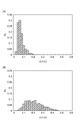
- Figure 33 is a variation [Delta] V (V) and the relative frequency of the operating voltage graph showing the relationship (product number ratio) F R ((A) discrete arrays, (B) a monolithic array).
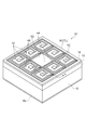
- FIG. 34 is a perspective view of the photodiode array.
- FIG. 35 is a vertical sectional view of the photodiode array taken along the line AA.
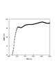
- FIG. 36 is a graph showing the relationship between the wavelength (nm) of incident light to SiCr and the transmittance (%).
- FIG. 37 shows (A) light detectors (50 ⁇ m spaced), (B) light detectors (25 ⁇ m spaced), (C) light detectors (20 ⁇ m spaced), (D) light detectors (15 ⁇ m spaced). : Type A), (E) Photodetectors (15 ⁇ m spacing: Type B), (F) Light detectors (10 ⁇ m spaced).
- FIG. 38 is a graph showing the relationship between the wavelength (nm) of incident light and the detection efficiency (%) of photons.
- FIG. 39 is a graph showing the relationship between the output of the photodiode and time.
- FIG. 40 is a diagram for explaining a photodiode manufacturing method.
- FIG. 41 is a longitudinal sectional view of a photodiode array in which the structure of the substrate is changed.
- FIG. 42 is a plan view of the photodiode array.
- FIG. 43 is a plan view of the photodiode array.
- FIG. 44 is a cross-sectional view of the photodiode array.
- FIG. 45 is a diagram illustrating a connection relationship between electrodes and wirings.
- FIG. 46 is a diagram illustrating a connection relationship between electrodes and wirings.
- FIG. 47 is a partial plan view of a photodiode array (first example).
- FIG. 48 is a cross-sectional view of the photodiode array (first example) taken along the line AA.
- FIG. 49 is a partial plan view of a photodiode array (second example).
- FIG. 50 is a cross-sectional view of the photodiode array (second example) taken along the line AA.
- FIG. 51 is a partial plan view of a photodiode array (third example).
- FIG. 52 is a cross-sectional view of the photodiode array (third example) taken along the line AA.
- FIG. 53 is a diagram showing a connection relationship between electrodes and wirings.
- FIG. 54 is a partial plan view of a photodiode array (fourth example).
- FIG. 55 is a cross-sectional view of the photodiode array (fourth example) taken along the line AA.
- FIG. 56 is a partial plan view of a photodiode array (fifth example).
- FIG. 57 is a cross-sectional view of the photodiode array (fifth example) taken along the line AA.
- FIG. 58 is a partial plan view of a photodiode array (sixth example).
- FIG. 59 is a cross-sectional view of the photodiode array (sixth example) taken along the line AA.
- FIG. 60 is a partial plan view of a photodiode array (seventh example).
- FIG. 61 is a cross-sectional view of the photodiode array (seventh example) taken along the line AA.
- FIG. 62 is a longitudinal sectional view of a photodiode array in which the structure of the substrate is changed.
- FIG. 63 is a plan view of the photodiode array.
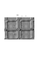
- FIG. 64 is a view showing an SEM photograph of the surface of the photodiode array.
- FIG. 65 is a view showing an SEM photograph of a cross section of the photodiode array.
- FIG. 66 is a plan view of a part of the photodiode array.
- 67 is a cross-sectional view of the photodiode array (second example) shown in FIG. 66 taken along the line AA.
- FIG. 68 is a graph (Example) showing the distance tp (ps) from the distance from each photodiode to the electrode pad (common electrode) and the reference of the signal transmission time.
- FIG. 69 is a graph (comparative example) showing the distance tp (ps) from the reference of the distance from each photodiode to the electrode pad (common electrode) and the signal transmission time.
- FIG. 70 is a graph showing the relationship between the voltage Vover and FWHM (ps).
- FIG. 71 is a graph showing the relationship between time t ⁇ (ps) and the number of counts.
- FIG. 72 is a diagram for explaining laser beam irradiation.
- FIG. 73 is a graph showing the relationship between time t ⁇ (ns) and output OUT (au).
- FIG. 74 is a cross-sectional view of the periphery of the common electrode.
- FIG. 75 is a sectional view of the periphery of the common electrode.
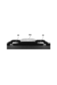
- FIG. 76 is a photograph showing a perspective configuration of the detector.
- the detector the PET apparatus, and the X-ray CT apparatus according to the embodiment will be described. Note that the same reference numerals are used for the same elements or elements having the same function, and redundant description is omitted.
- FIG. 1 is a schematic diagram of a subject diagnostic apparatus such as a PET apparatus / CT apparatus.
- the subject diagnosis apparatus includes a cradle 101, a gantry 102 having an opening in which the cradle 101 is located, and a control device 103.
- the control device 103 controls the drive motor 104 that moves the cradle 101 by a drive motor control signal, and changes the relative position of the cradle 101 with respect to the gantry 102.
- a subject 105 to be diagnosed is arranged on the cradle 101.
- the subject 105 is transported into the opening of the gantry 102 by the drive of the drive motor 104.
- the drive motor 104 may move the cradle 101, but may move the gantry 102.
- a plurality of detection devices 106 are arranged so as to surround the opening of the gantry 102.
- Each of the detection devices 106 includes a plurality of detectors D (see FIGS. 2 and 3).
- a control signal for controlling the detection device 106 is output from the control device 103 to the gantry 102, and a detection signal from the detection device 106 is input to the control device 103 from the gantry 102.
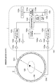
- FIG. 2 is a block diagram of a PET apparatus having the structure of FIG.
- a plurality of detectors D are arranged in a ring shape so as to surround the opening of the gantry.
- the subject 105 is injected with a radioactive isotope (RI) (positron emitting nuclide) that emits positrons (positrons).
- RI radioactive isotope
- Positrons combine with negative electrons in the body to generate annihilation radiation ( ⁇ rays). That is, ⁇ rays are emitted from the subject 105.
- the detector D detects the emitted ⁇ -rays, image-processes the detection signal by the image processing circuit 103g in the control device 103, and creates an image relating to internal information of the subject 105, that is, a tomographic image.
- the RI used in the PET apparatus is an element existing in the living body, such as carbon, oxygen, fluorine, and nitrogen.
- Gamma rays emitted from the subject 105 can be detected by a plurality of detectors D.
- this PET apparatus since the overall characteristics of the detector D are remarkably improved, it is possible to acquire a high-quality image.
- the detector D will be described later.
- ⁇ rays are emitted in one direction and in the opposite direction.
- the plurality of detectors D are arranged in a ring shape, and ⁇ -rays are incident on a specific detector D (n) and a detector D (k) facing the RI position across the RI position.
- n, k, and N are natural numbers.
- the TOF-PET apparatus includes a radiation detector array (detection apparatus 106) including a plurality of detectors D, a plurality of preamplifiers 103a and 103a ′, a plurality of sum amplifiers 103b and 103b ′, an energy discriminating circuit 103e, and a timing extraction. Circuits 103c and 103c ′ and a coincidence counting circuit 103f are provided.
- the subject 105 is disposed substantially at the center of the radiation detector array (detection device 106).
- a gamma ray pair is emitted from the subject 105.
- Gamma ray pairs are emitted in opposite directions.
- the plurality of detectors D are arranged on a circumference with the subject 105 as a substantial center.
- the detector D includes a scintillator that converts radiation ( ⁇ rays, X-rays) into fluorescence, and a photodetector that detects fluorescence.
- One detector D to which ⁇ rays are incident is connected to a plurality of preamplifiers 103a (one is representatively shown in the drawing), and each of the preamplifiers 103a is connected to both the sum amplifier 103b and the sum amplifier 103b2.
- the preamplifier 103a amplifies the output signal from the photodetector D at high speed, and the sum amplifiers 103b and 103b2 each output a logical sum of the output signals of the preamplifier 103a.
- the other detector D to which the ⁇ -rays enter is connected to a plurality of preamplifiers 103a ′ (one is representatively shown in the drawing), and each of the preamplifiers 103a ′ is a sum amplifier 103b ′ and a sum amplifier 103b2 ′. Connected to both.
- the preamplifier 103a ' amplifies the output signal from the photodetector D at high speed, and the sum amplifiers 103b' and 103b2 'each output a logical sum of the output signals of the preamplifier 103a'.
- the energy discriminating circuit 103e is connected to the sum amplifiers 103b2 and 103b2 '.
- the energy discriminating circuit 103e discriminates a signal equal to or higher than a predetermined threshold (hereinafter referred to as threshold SH) as a signal due to incidence of ⁇ rays, and outputs the discrimination result to the coincidence counting circuit 103f. That is, the operation result of the logical sum operation by the sum amplifiers 103b2 and 103b2 ′ is output to the energy discriminating circuit 103e. It is determined whether the signal is a signal, and the determination result is output to the coincidence counting circuit 103f.
- a predetermined threshold hereinafter referred to as threshold SH
- the threshold value SH is set in the vicinity of 511 keV, which is the photon energy of a pair of ⁇ rays generated with the annihilation of an electron / positron pair, for example.
- 511 keV is the photon energy of a pair of ⁇ rays generated with the annihilation of an electron / positron pair, for example.
- the energy discriminating circuit 103e includes a circuit that integrates signals output from the preamplifiers 103a and 103a 'via the sum amplifiers 103b2 and 103b2', and shapes a waveform so that the amplitude is proportional to the energy.
- Timing extraction circuits 103c and 103c ' output a first timing signal and a second timing signal based on signals output from the sum amplifiers 103b and 103b', respectively.
- the first and second timing signals are input to the coincidence counting circuit 103f.
- a timing extraction method a leading edge method or a constant fraction method can be used.
- the coincidence counting circuit 103f is connected to the energy discriminating circuit 103e and the timing extracting circuits 103c and 103c '.
- the coincidence circuit 103f determines whether or not the ⁇ -ray pair detected by the detectors D (n) and D (k) is a ⁇ -ray pair generated with the annihilation of the same electron / positron pair. This determination is made based on whether or not ⁇ rays have been detected by the other detector D (k) during a certain time before and after the detection time at which ⁇ rays have been detected by one detector D (n). . If it is detected under this condition, it can be determined that the pair of ⁇ -rays generated with the annihilation of the same electron / positron pair.
- the signals determined by the energy discriminating circuit 103e to have an energy level equal to or higher than the threshold value SH are Adopt as data.
- the true data is input to the image processing circuit 103g to create a tomographic image that is an image related to the internal information of the subject.
- the created image is stored in the storage device 103k and can be displayed on the display 103h.
- the storage device 103k stores a program for performing image processing and the like, and the program operates according to a command from a central processing unit (CPU) 103i.
- CPU central processing unit
- a series of operations necessary for inspection output of control signal (ON / OFF of detector) to detector D, control of drive motor, capture of detection signal from detector D, image processing after simultaneous counting, created image Storage in the storage device and display on the display
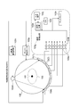
- FIG. 3 is a block diagram of an X-ray CT apparatus having the structure of FIG.
- the X-ray CT apparatus also includes a cradle and a gantry having the above-described structure, and the gantry includes an X-ray source 103m that emits X-rays.
- a plurality of detectors D are arranged at positions where X-rays from the X-ray source 103m are incident, and a detection device 106 is configured.
- a subject 105 is placed on the cradle 101 located in the opening of the gantry 102 in FIG. 1, and the subject 105 is irradiated with X-rays from an X-ray source 103m.
- X-rays transmitted through the subject 105 are detected by a plurality of detectors D, and an image relating to internal information of the subject 105, that is, a computer tomographic image, can be obtained by performing image processing on the detection signals.
- the control apparatus 103 can superimpose the image obtained by the PET apparatus and the image obtained by the X-ray CT apparatus.
- the detector D since the detector D whose overall characteristics are remarkably improved is used, it is possible to acquire a high-quality image.
- the subject 105 is arranged at the center of the detection device 106 arranged in a ring shape.
- the detection device 106 rotates around the rotation axis AX.
- the subject 105 is irradiated with X-rays, and the X-rays transmitted therethrough are incident on a plurality of detectors D (n).
- the output of each detector is input to the image processing circuit 103g via the preamplifier 103a and the sum amplifier 103b.
- the control device 103 of the X-ray CT apparatus includes a display 103h, a CPU 103i, a storage device 103k, and an input device 103j that function in the same manner as the PET apparatus.
- the program stored in the storage device 103k is activated, the X-ray source drive circuit 103n is controlled, and a drive signal is output from the drive circuit to the X-ray source 103m.
- the X-rays are emitted from the X-ray source 103m.
- the program stored in the storage device 103k is activated, the gantry drive motor 103p is driven, the detection device 106 is rotated around the rotation axis AX, and a control signal (detector ON / OFF) is detected by the detector.
- the detector D is turned ON, and the detection signal is input to the image processing circuit 103g via the preamplifier 103a and the sum amplifier 103b.
- the image processing circuit 103g creates a computer tomographic image in accordance with the tomographic image creation program input to the storage device 103k.
- the created image is stored in the storage device 103k and can be displayed on the display 103h.
- the storage device 103k stores a program for performing image processing and the like, and the program operates according to a command from the central processing unit (CPU) 103i.
- a series of operations necessary for inspection output of control signals (ON / OFF of detector) to detector D, control of various drive motors, capture of detection signals from detector D, image processing of detection signals, created image Storage in the storage device and display on the display) can be performed by the input device 103j.
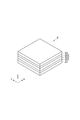
- FIG. 4 is a perspective view of the detector D.
- FIG. 4 is a perspective view of the detector D.
- the detector D includes a wiring board 20 and a plurality of detection chips S (semiconductor chips S1) arranged and fixed on the wiring board 20 so as to be two-dimensionally spaced from each other.
- a first bump electrode BE and a second bump electrode B2 are interposed between each detection chip S (semiconductor chip S1) and the wiring board 20.
- 4 ⁇ 4 detection chips S are arranged, but as long as there are a plurality of detection chips S, other numbers can naturally be employed.
- an XYZ three-dimensional orthogonal coordinate system is shown, but the opening center (subject 105) of the gantry is located on the extended line in the + Z direction.
- ⁇ -rays or X-rays travel in the negative direction of the Z-axis and enter the detection chip S, and the output signal is input to the wiring board 20 via the bump electrodes, and the output from the wiring board 20 is the aforementioned. Input to the preamplifier.
- FIG. 5 is a diagram for explaining the interval between the detection chips S in the detector D.
- the detection chip S is arranged at a distance d1 in both the X-axis direction and the Y-direction.
- the detection chip S is provided with a scintillator on the semiconductor chip S1, but the scintillator is not shown in the figure.
- the semiconductor chip S1 has a semiconductor region 14 serving as a detection channel on the surface side.
- the semiconductor region 14 is a region on the surface side of a region that forms a pn junction with the semiconductor substrate in the semiconductor chip S1.
- d2 be the minimum value of the separation distance of the semiconductor regions 14 between the adjacent semiconductor chips S1.
- One semiconductor chip S1 has a plurality of semiconductor detection regions 14 in a two-dimensional shape. However, when a group of semiconductor regions 14 is one detection channel and a single detection channel is provided, a detector is provided. D constitutes a discrete array.
- one semiconductor chip S1 includes a plurality of detection channels, a monolithic array is configured.
- high-concentration impurities (the same conductivity type as that of the semiconductor substrate: N-type) are added to the side surfaces of the semiconductor chip to form an impurity-added region IS.
- high-concentration impurities the same conductivity type as that of the semiconductor substrate: N-type
- the separation distance between the detection channels in the case of the monolithic array (the minimum value of the distance between the semiconductor regions 14 in the adjacent detection channels) can be set equal to the distance d1. In this case, there is an advantage that the separation distances of all the semiconductor regions 14 are equal.
- FIG. 6 is a perspective view of the detector D '.
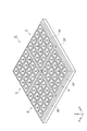
- a plurality of wiring boards 20 shown in FIG. 4 are arranged and fixed on the main wiring board or the support board 20 ′, and 8 ⁇ 8 detection chips S are arranged as a whole. By adopting such a configuration, an increase in the size of the detector can be achieved.
- FIG. 7 is a perspective view of the detector D ′′.
- FIG. 76 is a photograph showing a perspective configuration of a detector in which a plurality of detection chips are arranged, and a detector having a larger area could be prototyped.
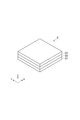
- FIG. 8 is a perspective view of the detection chip S.
- a scintillator S3 is provided on the semiconductor chip S1 via an adhesive layer S2.
- the adhesive layer S2 is a resin such as Epo-Tek301 (trademark) manufactured by Epoxy Technologies.
- the scintillator S3 includes Lu 2 -x Y x SiO 5 : Ce (LYSO), gadolinium aluminum gallium garnet (GAGG), NaI (TI), Pr: LuAG, LaBr 2 , LaBr 3 , and (Lu x Tb 1-x- y Ce y ) 3 Al 5 O 12 (that is, LuTAG), at least one selected from the group consisting of two or a mixture of any two or more thereof.
- the Lu composition ratio “x” is in the range of 0.5 to 1.5
- the Ce composition ratio “y” is in the range of 0.01 to 0.15.
- FIG. 9 is a perspective view of a detection chip S having another structure.
- a glass plate S22 is provided on the semiconductor chip S1 via an adhesive layer S21.
- a scintillator S3 is provided on the glass plate S22 via an adhesive layer S23.
- the materials for the adhesive layer and scintillator are as described above. The radiation incident on the scintillator S3 is converted into fluorescence by the scintillator S3, and enters the semiconductor chip S1 through the adhesive layer S23, the glass plate S22, and the adhesive layer S21.
- the scintillator S3 is located on the surface of each semiconductor chip S1 via the insulators (S2, S21, S22, S23).
- the scintillator S3 generates light having a longer wavelength than these in accordance with the incidence of radiation such as X-rays or ⁇ -rays incident thereon.
- radiation such as X-rays or ⁇ -rays incident thereon.
- the insulator is made of a glass plate or a resin, and protects the surface of the APD, and the light from the scintillator can be slightly diffused before reaching the APD.
- the resin can also have an adhesion function between the scintillator and the semiconductor chip.
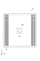
- FIG. 10 is a plan view of the semiconductor chip S1.
- a plurality of light detection units 10 are arranged on the surface of the semiconductor chip S1 along the X axis and the Y axis.
- a common electrode E3 for collecting signals from the respective light detection units 10 is arranged in the central part of the semiconductor chip S1.
- the light detection part 10 is formed on the whole surface of the semiconductor chip S1, the light detection part 10 is illustrated only in the vicinity of both ends for the sake of clarity of the common electrode.
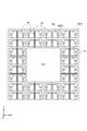
- FIG. 11 is an enlarged view of the common electrode peripheral portion (region RS1 in FIG. 10) of the semiconductor chip S1.
- the light detection unit 10 includes an APD and a quenching resistor R1 (resistance layer) connected to one end (anode) of the APD.
- the quenching resistor R1 is connected to the common electrode E3 via the readout wiring TL. That is, all the APDs in the plurality of light detection units 10 are all connected to the common electrode E3 via the quenching resistor R1 and the readout wiring TL.
- FIG. 12 is a circuit diagram of the detector.
- the semiconductor chip S1 includes one or a plurality of photodiode arrays PDA.
- the photodiode array PDA includes a plurality of light detection units 10 (APD, quenching resistor R1).
- APD light detection units 10
- each APD is operated in the Geiger mode.
- a reverse voltage (reverse bias voltage) larger than the breakdown voltage of the APD is applied between the anode / cathode of the APD. That is, the ( ⁇ ) potential V1 is applied to the anode and the (+) potential V2 is applied to the cathode.
- the polarities of these potentials are relative, and one of the potentials can be a ground potential.
- the wiring board 20 may be provided with a signal processing unit SP for processing a signal from the photodiode array PDA.
- the signal processing unit SP constitutes an ASIC (Application Specific Integrated Circuit).
- the signal processing unit SP can include a CMOS circuit that converts an output signal from the photodiode array PDA (channel) into a digital pulse.
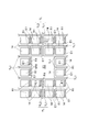
- FIG. 13 is a plan view of the light detection portion around the common electrode.
- the APD has electrodes E1 arranged on the main surface side of the semiconductor substrate.
- the electrode E1 is electrically connected to the second semiconductor region 14.
- the first semiconductor region located immediately below the second semiconductor region 14 is electrically connected to the electrode E1 through the second semiconductor region 14.
- a readout wiring (signal line) TL and a common electrode E3 are formed via an insulating layer.
- the common electrode E3 is located in the central region of each channel (photodiode array PDA).
- the readout wiring TL includes a plurality of signal lines TL1 and a plurality of signal lines TL2. Each signal line TL1 extends in the Y-axis direction between adjacent APDs in plan view. Each readout wiring TL2 extends between adjacent APDs in the X-axis direction, and electrically connects the plurality of readout wirings TL1.
- the read wiring TL2 is connected to the common electrode E3.
- the read line TL1 is electrically connected to the common electrode E3 via the read line TL2, except for the line directly connected to the common electrode E3.
- the photodiode array PDA has a quenching resistor R1 formed on the semiconductor substrate outside the second semiconductor region 14 via an insulating layer for each APD. That is, the quenching resistor R1 is arranged on the main surface side of the semiconductor substrate. The quenching resistor R1 has one end connected to the electrode E1 and the other end connected to the readout wiring TL1.
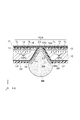
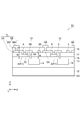
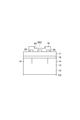
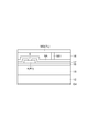
- FIG. 14 is a sectional view of the periphery of the common electrode.
- the semiconductor region 12 constituting the semiconductor substrate includes a main surface 1Na and a main surface 1Nb facing each other.
- the semiconductor region 12 is an N-type (first conductivity type) semiconductor substrate made of Si.
- Each photodiode array PDA includes a plurality of APDs formed in the semiconductor region 12.
- the anode of the APD is a P-type semiconductor region 13 (14), and the cathode is an N-type semiconductor region 12.
- Avalanche multiplication is performed in a region near the pn junction interface of the first semiconductor region 13, and the amplified electron group flows toward an electrode formed on the back surface of the semiconductor region 12. That is, when a photon is incident on any pixel (avalanche photodiode APD) of the photodiode array PDA, the photon is multiplied and extracted as a signal from the electrode E3 (through electrode TE).
- a quenching resistor R1 is connected in series to each APD.
- One APD constitutes one pixel in each photodiode array PDA.
- Each APD is connected in parallel with each other in series with the quenching resistor R1, and a reverse bias voltage is applied from the power source.
- Each APD has a P-type (second conductivity type) first semiconductor region 13 and a P-type (second conductivity type) second semiconductor region 14.
- the first semiconductor region 13 is formed on the main surface 1Na side of the semiconductor region 12.
- the second semiconductor region 14 is formed in the first semiconductor region 13 and has a higher impurity concentration than the first semiconductor region 14.
- the planar shape of the second semiconductor region 14 is, for example, a polygon (in this embodiment, a quadrangle).
- the first semiconductor region 13 is deeper than the second semiconductor region 14.
- the semiconductor region 12 has an N-type (first conductivity type) semiconductor region 1PC.
- the semiconductor region 1PC is formed on the main surface 1Na side of the semiconductor region 12.
- the semiconductor region 1PC prevents the PN junction formed between the N-type semiconductor region 12 and the P-type first semiconductor region 13 from being exposed to the through hole TH in which the through electrode TE is disposed.
- the semiconductor region 1PC is formed at a position corresponding to the through hole TH (through electrode TE).
- the insulating layer 16 is formed on the surface of the second semiconductor region 14, and the common electrode E3 and the readout wiring TL are formed thereon.
- the common electrode E3 and the readout wiring TL are covered with an insulating layer 17.
- the back surface 1Nb of the semiconductor region 12 is covered with an insulating layer L3.
- the insulation L3 has an opening, and the through electrode TE passes through the opening.
- the common electrode E3 is in contact with and electrically connected to the through electrode TE, and the first bump electrode BE is in contact with the through electrode TE through the under bump metal BM.
- the inner surface of the through hole TH provided in the semiconductor region 12 is covered with the insulating layer L2, and the insulating layer L2 is continuous with the insulating layer L3.
- the through electrode TE and the insulating layer L3 are covered with a passivation film (protective film) PF.
- An electroless plating method can be used as a method for forming the UBM.
- a method for forming the bump electrode BE a method of mounting a solder ball or a printing method can be used.
- each semiconductor chip includes a semiconductor region 12 having a plurality of photodetecting portions 10 arranged two-dimensionally, an insulating layer 16 formed on the surface of the semiconductor region 12, and the insulating layer 16
- the common electrode E3 disposed in the first electrode, the quenching resistor R1 of each of the light detection units 10 and the common electrode E3, and the common electrode E3 through the through hole TH of the semiconductor region 12 from the common electrode E3.
- a through electrode TE extending on the back surface of the semiconductor region 12.
- Each photodiode array PDA includes a through electrode TE.
- the through electrode TE is provided for each individual photodiode array PDA, that is, for each individual channel.
- the through electrode TE is formed to penetrate the semiconductor region 12 from the main surface 1Na side to the main surface 1Nb side. That is, the through electrode TE is disposed in the through hole TH that penetrates the semiconductor region 12.
- the insulating layer L2 is also formed in the through hole TH. Therefore, the through electrode TE is disposed in the through hole TH via the insulating layer L2.
- the through electrode TE has one end connected to the common electrode E3, and connects the readout wiring TL and the through electrode TE.
- Each photodetection unit 10 includes an APD, and each APD forms a first conductivity type semiconductor region 12 (first semiconductor region) and a pn junction with the semiconductor region 12 and outputs carriers.
- a second semiconductor region (13, 14) of the second conductivity type is provided.
- a quenching resistor R1 is electrically connected to the second semiconductor region 14 of the APD.
- the first bump electrode BE electrically connects the through electrode TE and the wiring substrate 20, and the second bump electrode B2 (see FIG. 15 and the like) is connected to the semiconductor region 12 (first semiconductor region) of the APD and the wiring.
- the substrate 20 is electrically connected.
- the quenching resistor R1 has a higher resistivity than the electrode E1 and the common electrode E3 to which it is connected.
- Quenching resistor R1 is made of, for example, polysilicon.
- a CVD (Chemical Vapor Deposition) method can be used as a method of forming the quenching resistor R1.
- SiCr, NiCr, TaNi, FeCr, etc. are mentioned as a resistor which comprises quenching resistance R1.
- the electrodes E1, E3 and the through electrode TE are made of a metal such as aluminum.
- the semiconductor substrate is made of Si, AuGe / Ni or the like is often used as the electrode material in addition to aluminum.
- a sputtering method can be used as a method for forming the electrodes E1, E3 and the through electrode TE.
- a Group 3 element such as B is used as the P-type impurity, and a Group 5 element such as N, P, or As is used as the N-type impurity. Even if N-type and P-type semiconductors are substituted for each other to form an element, the element can function.
- a diffusion method or an ion implantation method can be used as a method for adding these impurities.
- SiO 2 or SiN can be used as a material of the above-described insulating layer.
- a method for forming the insulating layer when each insulating layer is made of SiO 2 , a thermal oxidation method or a sputtering method can be used. .
- an APD is formed by forming a pn junction between the N-type semiconductor region 12 and the P-type first semiconductor region 13.
- the semiconductor region 12 is directly connected to the back surface of the substrate 1N or electrically connected to an electrode (not shown) formed on the back surface.
- the first semiconductor region 13 is connected to the wiring substrate 20 through the second semiconductor region 14, the electrode E1, the quenching resistor R1, the readout wiring TL, the common electrode E3, the through electrode TE, and the bump electrode BE in this order.
- the back surface of the semiconductor region 12 is connected to the wiring substrate 20 via the bump electrode B2.
- the quenching resistor R1 is connected in series with the APD.
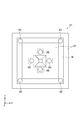
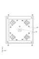
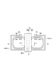
- FIG. 15 is a bottom view of the semiconductor chip S1 of FIG.
- the second bump electrode B2 is disposed in this exposed region. In the center of the semiconductor region 12, the first bump electrode BE is located.
- the second bump electrode B ⁇ b> 2 is disposed at a position corresponding to the four corners of the rectangular semiconductor region 12.
- FIG. 16 is a bottom view of the semiconductor chip S1 according to the improvement.
- this structure is such that a conductive film M is formed on the back surface of the semiconductor region 12 exposed by removing the passivation film PF, and a bump electrode B2 is disposed on the conductive film M.
- the other points are the same.
- the shape of the conductive film M is rectangular, and the material can be the same as the electrode material. Note that solder can be used as the material of the bump electrode.
- a bias voltage that operates in the Geiger mode is applied to both ends of the APD included in each light detection unit 10 via the first bump electrode BE and the second bump electrode B2.
- Carriers generated in the plurality of APDs due to the incidence of light (energy rays) flow to the common electrode E3 on the semiconductor region 12 through the respective quenching resistors R1, and from the common electrode E3 to the through electrode TE and the first electrode. It reaches the wiring board 20 through the bump electrode BE and is taken out to the outside.
- the APD having the structure has a carrier transmission path shortening structure using a through electrode or the like, the wiring resistance is reduced. Therefore, the transmission speed of the carrier from the APD, that is, the time resolution is improved.
- the time resolution is improved, so that more accurate photon detection can be performed. In another semiconductor chip, it is not guaranteed that the same time resolution is obtained due to a manufacturing error or the like.
- a semiconductor chip having a product characteristic within a certain range is selected and wiring is performed. Bonding to the substrate via the bump electrode reduces the characteristic variation for each semiconductor chip.
- the two-dimensionally arranged semiconductor chips S1 are separated from each other, the influence of light incident on a specific semiconductor chip leaking to other semiconductor chips and causing crosstalk is suppressed, and between the semiconductor chips.
- This gap can alleviate the influence of the warping of the wiring board due to the expansion / contraction of the wiring board 20 on the semiconductor chip. That is, characteristics such as time resolution, crosstalk, and resistance to temperature change as a whole detector are remarkably improved.
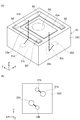
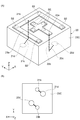
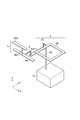
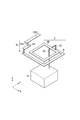
- FIG. 17 is a perspective view (A) and a bottom view (B) of the basic components of the wiring board.
- the wiring substrate 20 is provided on the surface of the insulating substrate 20C, and includes an electrode 20a that contacts the first bump electrode BE and an electrode 21a that contacts the four second bump electrodes B2.
- an electrode pad 20d that is electrically connected to the electrode 20a is provided via a through electrode 20b that passes through the inside of the insulating substrate 20C.
- the through electrode 20b and the electrode pad 20d are connected via the connection electrode 20c.
- an electrode pad 21d that is electrically connected to the electrode 21a is provided via a through electrode 21b that passes through the inside of the insulating substrate 20C.
- the through electrode 21b and the electrode pad 21d are connected via the connection electrode 21c.
- the electrodes provided on the insulating substrate 20C are all printed wiring patterns.
- the shape of the first electrode 20a on the surface is a quadrangle, and the second electrode 21a is adjacent to and surrounds the three sides of the first electrode 20a.
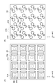
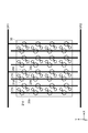
- FIG. 18 is a plan view (A) and a bottom view (B) of the wiring board.
- This wiring board 20 is obtained by arranging a plurality of wiring patterns shown in FIG. 17 along the X axis and the Y axis.
- the left two rows of the second electrodes 21a are arranged so that the lower side is open, but the right two rows of the second electrodes 21a have an axis parallel to the thickness of the wiring board. It is rotated 180 ° in the center and is arranged so that the upper side is open.
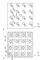
- FIG. 19 is a plan view (A) and a bottom view (B) of the wiring board.
- the wiring board 20 has a plurality of wiring patterns shown in FIG. 17 arranged along the X axis and the Y axis, and at the same time, the second electrodes 21a adjacent to each other in the X axis direction are continuously arranged. This is the electrode 210a.
- the electrode 210a extends along the Y axis, and all the second electrodes 21a are electrically connected on the surface side. In this case, there is an advantage that the structure is simplified because the through electrode 210d may be provided directly below one of the electrodes 210a and exposed on the back surface.
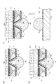
- FIG. 20 is a cross-sectional view of the periphery of the common electrode.
- the first bump electrode BE is disposed in the through hole provided in the semiconductor region 12, but may be provided at a position different from this.
- the through electrode TE is located on the insulating layer L3 on the back surface of the semiconductor substrate along the inner surface of the through hole.
- a contact hole is formed in the insulating layer L3 to expose the through electrode TE, and the first bump electrode BE can be provided on the exposed surface via the amber bump electrode metal BM.
- the under bump metal BM can be provided so as to contact the through electrode TE in the removed region by removing the passivation film PF at the bottom of the through hole TH.
- a bump electrode can also be arranged on the bottom under bump metal BM.
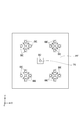
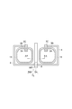
- FIG. 21 is a bottom view of the semiconductor chip S1 of FIG.
- the second bump electrode B2 is disposed in this exposed region.
- Four first bump electrodes BE are located around the center of the semiconductor region 12.
- the second bump electrode B ⁇ b> 2 is disposed at a position corresponding to the four corners of the rectangular semiconductor region 12.
- the first bump electrode BE is provided so that the opening shape is adjacent to each side of the rectangular through hole.
- the shape of the through hole is a square pyramid.
- FIG. 22 is a bottom view of the semiconductor chip S1 according to the improvement.
- this structure is such that a conductive film M is formed on the back surface of the semiconductor region 12 exposed by removing the passivation film PF, and a bump electrode B2 is disposed on the conductive film M.
- the other points are the same.
- the shape of the conductive film M is rectangular, and the material can be the same as the electrode material. Note that solder can be used as the material of the bump electrode.
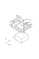
- FIG. 23 is a perspective view (A) and a bottom view (B) of the basic components of the wiring board.
- the wiring substrate 20 is provided on the surface of the insulating substrate 20C and includes an electrode 20a that contacts the four first bump electrodes BE and an electrode 21a that contacts the four second bump electrodes B2.
- an electrode pad 20d that is electrically connected to the electrode 20a is provided via a through electrode 20b that passes through the inside of the insulating substrate 20C.
- the through electrode 20b and the electrode pad 20d are connected via the connection electrode 20c.
- an electrode pad 21d that is electrically connected to the electrode 21a is provided via a through electrode 21b that passes through the inside of the insulating substrate 20C.
- the through electrode 21b and the electrode pad 21d are connected via the connection electrode 21c.
- the electrodes provided on the insulating substrate 20C are all printed wiring patterns.
- the shape of the first electrode 20a on the surface is a cruciform shape, and the second electrode 21a is adjacent to the first electrode 20a and has a substantially U-shape with one end open while surrounding the first electrode 20a.
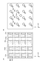
- FIG. 24 is a plan view (A) and a bottom view (B) of the wiring board.
- This wiring board 20 is obtained by arranging a plurality of wiring patterns shown in FIG. 23 along the X axis and the Y axis.
- the left two rows of the second electrodes 21a are arranged so that the lower side is open, but the right two rows of the second electrodes 21a have an axis parallel to the thickness of the wiring board. It is rotated 180 ° in the center and is arranged so that the upper side is open.
- FIG. 25 is a bottom view of the wiring board.
- the wiring SR1 that connects the electrode pads 20d and the wiring SR2 that connects the electrode pads 21d may be provided. Thereby, the output from each 1st bump electrode BE can be output outside via wiring SR1, and the output from 2nd bump electrode B2 can be output outside via wiring SR2.
- FIG. 26 is a plan view (A) and a bottom view (B) of the wiring board.
- the wiring board 20 has a plurality of wiring patterns shown in FIG. 23 arranged along the X axis and the Y axis, and at the same time, the second electrodes 21a adjacent to each other in the X axis direction are continuously arranged. This is the electrode 210a.
- the electrode 210a extends along the Y axis, and all the second electrodes 21a are electrically connected on the surface side. In this case, there is an advantage that the structure is simplified because the through electrode 210d may be provided directly below one of the electrodes 210a and exposed on the back surface.
- FIG. 27 is a plan view of the semiconductor chip S1.
- a plurality of light detection units 10 are arranged on the surface of the semiconductor chip S1 along the X axis and the Y axis.
- a plurality of common electrodes E3 from which signals from the respective light detection units 10 are collected are arranged in the central part of the semiconductor chip S1.
- the light detection part 10 is formed on the whole surface of the semiconductor chip S1, the light detection part 10 is illustrated only in the vicinity of both ends for the sake of clarity of the common electrode.
- each common electrode E3 is shown in the semiconductor chip S1.
- the cross-sectional structure of the peripheral region RS1 of each common electrode E3 is the same as that shown in FIG.
- FIG. 28 is a bottom view of the semiconductor chip S1 shown in FIG.
- the number of first bump electrodes BE is four for each common electrode, but the one used in FIG. 14 is adopted. In this case, the number of first bump electrodes BE is one for each common electrode.
- Second bump electrodes B2 are arranged at five locations in the exposed region.
- the second bump electrodes B2 are disposed at positions corresponding to the four corners and the center of the rectangular semiconductor region 12.
- Four first bump electrodes BE are located at locations corresponding to the four common electrodes in the semiconductor region 12.
- FIG. 29 is a bottom view of the semiconductor chip S1 according to the improvement.
- the semiconductor chip S1 is different from that shown in FIG. 28 in that the second bump electrode B2 is provided only at one central position of the semiconductor chip S1, and the other configuration is that shown in FIG. Is the same.
- first semiconductor region 13, second semiconductor region 14, insulating layer 16, quenching resistor R1, electrodes E1, E3, and signal line TL) corresponding to each channel (photodiode array PDA) were formed.
- a semiconductor region 12 is prepared.
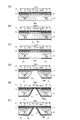
- the insulating layer 17 is formed on the main surface 1Na side of the semiconductor region 12, and then the semiconductor region 12 is thinned from the main surface 1Nb side (see FIG. 30A).
- Insulating layer 17 is made of SiO 2.
- a CVD (Chemical Vapor Deposition) method can be used.
- a mechanical polishing method or a chemical polishing method can be used as a thinning method of the semiconductor region 12.
- an insulating layer L3 is formed on the back surface 1Nb side of the prepared semiconductor region 12 (see FIG. 30B).
- Insulating layer L3 is made of SiO 2.
- a CVD (Chemical Vapor Deposition) method can be used as a method of forming the insulating layer L3.
- a region where the through hole TH is formed in the insulating layer L3 is removed (see FIG. 30C).
- a dry etching method can be used as a method for removing the insulating layer L3.
- a through hole TH for arranging the through electrode TE is formed in the semiconductor region 12 (see FIG. 30D).
- a dry etching method and a wet etching method can be appropriately selected and applied.
- the insulating layer 16 functions as an etching stop layer. Since an undercut occurs in the insulating layer L3 when the through hole is formed by alkali etching, the insulating layer L3 is etched by a dry etching method. At this time, the insulating layer 16 is also etched at the same time.
- a part of the insulating layer L2 is removed to expose the electrode E3 (FIG. 30E). reference).
- a dry etching method can be used as a method for removing the insulating layer L1 and the insulating layer L2.
- the through electrode TE is formed (see FIG. 30F)).
- the through electrode TE can be formed by sputtering.
- a passivation film PF having an opening formed at a position corresponding to the bump electrode BE is formed on the main surface 1Nb side of the semiconductor region 12, and then the bump electrode BE is formed (see FIG. 31G). Thereby, a semiconductor chip is obtained.
- an under bump metal BM is formed in a region exposed from the passivation film PF in the through electrode TE.
- the BM is made of a material that is electrically and physically connected to the bump electrode BE.
- an electroless plating method can be used.
- a method for forming the bump electrode BE a method of mounting a solder ball or a printing method can be used.
- the glass substrate S22 is bonded to the semiconductor chip S1 through an optical adhesive (see FIG. 31 (H)). Thereby, the glass substrate S22 and the semiconductor chip S1 are optically connected.
- the glass substrate S22 is also prepared in the form of a glass substrate base material including a plurality of glass substrates. The step of bonding the glass substrate S22 and the semiconductor chip S1 may be performed after the insulating layer L3 is formed in the semiconductor region 12. In addition, when it is not necessary to use the glass substrate S22, it can be omitted.
- the laminated body composed of the glass substrate S22 (glass substrate base material) and the semiconductor chip S1 (semiconductor wafer) is cut by dicing. Thereby, the side surface of the semiconductor region 12 and the side surface 30c of the glass substrate S22 are flush with each other.
- the bumps are connected to the semiconductor photodetector 10 with the glass substrate S22 facing and the mounting substrate 20 prepared separately (see FIG. 31I). By these processes, the detection chip S is obtained.
- a bump electrode BE is formed at a position corresponding to the electrode 20a on the main surface 20U side, and a signal extraction electrode is formed on the opposite surface 20D.
- the photodiode array PDA When the photodiode array PDA is used as one channel and a plurality of channels are provided, a detection chip with a large area can be realized.
- a through electrode TE that is electrically connected to the signal line TL and penetrates from the main surface 1Na side to the main surface 1Nb side is formed in the semiconductor region 12 for each channel, and the through electrode TE and the electrode of the wiring substrate 20 are bumped. It is electrically connected via an electrode.
- the detection chip S includes a glass substrate S22 arranged on the main surface 1Na side of the semiconductor region 12. Thereby, the mechanical strength of the semiconductor region 12 can be increased by the glass substrate S22.
- the side surface of the semiconductor region 12 and the side surface of the glass substrate S22 are flush with each other. Thereby, dead space can be reduced.
- the main surface 30b of the glass substrate S22 is flat. Thereby, the scintillator can be installed on the glass substrate S22 very easily.
- the through electrode TE is located in the central region of each channel. Thereby, in each channel, the wiring distance from each APD to the penetration electrode TE can be shortened.
- the semiconductor chip S1 is disposed on the main surface 1Na side of the semiconductor region 12, and includes a common electrode E3 that connects the signal line TL and the through electrode TE. Thereby, the signal line TL and the through electrode TE can be reliably electrically connected.
- the through electrode TE may be located in a region between each channel (photodiode array PDA). In this case, it is possible to prevent a decrease in the aperture ratio in each channel.
- the bump electrode BE may be disposed outside the through hole TH.
- a plurality of bump electrodes (four bump electrodes in this example) BE are formed for one through electrode TE.
- the bump electrode BE can be disposed on an electrode portion that is continuous with the through electrode TE and is disposed on the main surface 1Nb side of the semiconductor region 12.
- the shape of the semiconductor regions 13 and 14 is not limited to the shape described above, and may be other shapes (for example, a circular shape). Further, the number (number of rows and number of columns) and arrangement of APDs (second semiconductor regions 14) are not limited to those described above. Further, the number and arrangement of channels (PDA) are not limited to those described above.
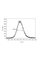
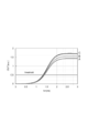
- Figure 32 is a graph showing the relationship between the number of photons N P and the signal intensity I S (a.u.) incident simultaneously.
- the cell pitch is the distance between the centers of the adjacent light detection units 10.
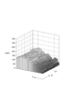
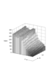
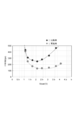
- Figure 33 is a graph voltage variation ⁇ V (V) and shows the relationship between relative frequency F R ((A) discrete arrays, (B) a monolithic array).
- the relative frequency F R denotes the number of occurrences of the voltage variation ⁇ V in the array.
- a common bias potential is applied to the cathode of the APD of the semiconductor chip, and the applied voltage is common to all APDs.
- the voltage gain variation is large in the monolithic array type in which 3 ⁇ 3 mm active channels 4 rows and 4 columns are arranged on the same semiconductor chip.
- the voltage variation of all 16 channels (semiconductor chips) averages 0.21 V (FIG. 33B).
- FIG. 34 is a perspective view of the photodiode array
- FIG. 35 is a vertical cross-sectional view of the photodiode array along the line AA.
- This photodiode array has a light receiving region on the surface side of a semiconductor substrate made of Si.
- the light receiving area includes a plurality of light detection units 10, and these light detection units 10 are two-dimensionally arranged in a matrix.
- the light detection units 10 in 3 rows and 3 columns are arranged, and these constitute a light receiving region, but the number of the light detection units 10 may be larger or smaller, A one-dimensionally arranged configuration is also possible.
- a signal reading wiring pattern (upper surface electrode) 3C (reading wiring TL) is arranged in a lattice pattern.
- FIG. 34 the illustration of the insulating layer 17 shown in FIG. 35 is omitted so that the internal structure can be understood.
- a light detection region is defined in the opening of the grid-like wiring pattern 3C.
- the light detection unit 10 is disposed in the light detection region, and the output of the light detection unit 10 is connected to the wiring pattern 3C.
- the lower surface electrode E4 is provided on the back surface of the substrate as required, but may not be used when the contact resistance between the bump electrode provided on the back surface and the semiconductor substrate is small. Therefore, if the drive voltage of the photodetection unit 10 is applied between the wiring pattern 3C that is the upper surface electrode and the lower surface electrode E4, the light detection output can be taken out from the wiring pattern 3C.
- the p-type semiconductor region constituting this constitutes an anode
- the n-type semiconductor region constitutes a cathode.
- the drive voltage is a reverse bias voltage applied to a photodiode formed by an internal pn junction in the light detection unit 10.
- This drive voltage is set to be equal to or higher than the breakdown voltage of the photodiode, an avalanche breakdown occurs in the photodiode, and the photodiode operates in the Geiger mode. That is, each photodiode is an avalanche photodiode (APD). Even when a forward bias voltage is applied to the photodiode, the photodiode has a light detection function.
- a resistor portion (quenching resistor R1) 4 electrically connected to one end of the photodiode is disposed on the substrate surface.
- One end of the resistor section 4 constitutes a contact electrode 4A that is electrically connected to one end of the photodiode via a contact electrode made of another material located immediately below this, and the other end is used for signal readout.
- a contact electrode 4C is formed in contact with and electrically connected to the wiring pattern 3C. That is, the resistance part 4 in each photodetection part 10 is connected to the contact electrode 4A connected to the photodiode, the resistance layer 4B extending in a curve continuously to the contact electrode 4A, and the terminal part of the resistance layer 4B.
- a contact electrode 4C is provided. Note that the contact electrode 4A, the resistance layer 4B, and the contact electrode 4C are composed of resistance layers of the same resistance material, and these are continuous.
- the resistance portion 4 extends in a curved manner from an electrical connection point with the photodiode, and is connected to the signal reading wiring pattern 3C. Since the resistance value of the resistance unit 4 is proportional to its length, the resistance value can be increased by extending the resistance unit 4 in a curved line. In addition, the presence of the resistance portion 4 can stabilize the surface level of the semiconductor region existing thereunder and stabilize the output.
- the wiring pattern 3C includes a shape surrounding the individual light detection units 10, but the shape of the wiring pattern 3C is not limited to this, and for example, two or more light detection units 10 or a shape surrounding one or more rows of the light detection units 10 (see FIG. 42).
- FIG. 42 a plurality of rows of photodetecting portions are grouped into one group, and a wiring pattern 3C (reading wiring TL) extends therebetween.
- the surface level of the semiconductor region 14 can be further stabilized by disposing the resistance layer 4B so as to cover the edge of the semiconductor region 14 in each photodetector. More specifically, the resistance layer 4B is disposed on the outline of the semiconductor region 14 as viewed from the thickness direction.
- one end of the photodiode included in the light detection unit 10 is connected to the wiring pattern 3C having the same potential at all positions, and the other end is connected to the lower surface electrode E4 that applies the substrate potential. That is, the photodiodes in all the light detection units 10 are connected in parallel.
- a common electrode E3 is provided on the surface of the semiconductor chip S1, and all the readout wirings TL are connected to the common electrode E3.
- the cross-sectional structure around the common electrode E3 and the structure of the wiring board disposed under the bump electrode are the same as those described above.
- each contact electrode 4A is located at the center of each photodetection region surrounded by the wiring pattern 3C.
- the two-dimensional pattern of the resistance portion 4B includes a shape extending so as to rotate around the contact electrode 4A.
- each of the light detection units 10 includes a first conductivity type (n-type) first semiconductor region (layer) 12 and a second conductivity type that forms a pn junction with the first semiconductor region 12.
- a p-type second semiconductor region semiconductor layer 13 and high impurity concentration region 14 is provided.
- the first contact electrode 3A is in contact with the high impurity concentration region (semiconductor region) 14 in the second semiconductor region.
- the high impurity concentration region 14 is a diffusion region (semiconductor region) formed by diffusing impurities into the semiconductor layer 13, and has a higher impurity concentration than the semiconductor layer 13.
- a p-type semiconductor layer 13 is formed on the n-type first semiconductor region 12, and a p-type high-concentration impurity region 14 is formed on the surface side of the semiconductor layer 13. . Therefore, the pn junction constituting the photodiode is formed between the first semiconductor region 12 and the semiconductor layer 13.
- the layer structure of the semiconductor substrate As the layer structure of the semiconductor substrate, a structure in which the conductivity type is reversed from the above can be adopted. That is, in the (type 2) structure, the n-type semiconductor layer 13 is formed on the p-type first semiconductor region 12, and the n-type high-concentration impurity region 14 is formed on the surface side of the semiconductor layer 13. Formed.
- the pn junction interface can be formed on the surface layer side.
- the n-type semiconductor layer 13 is formed on the n-type first semiconductor region 12, and the p-type high-concentration impurity region 14 is formed on the surface side of the semiconductor layer 13. It becomes a structure to be.
- the pn junction is formed at the interface between the semiconductor layer 13 and the semiconductor region 14.
- the conductivity type can be reversed. That is, in the (type 4) structure, the p-type semiconductor layer 13 is formed on the p-type first semiconductor region 12, and the n-type high concentration impurity region 14 is formed on the surface side of the semiconductor layer 13. It becomes a structure.
- FIG. 41 can also be employed as the structure of the semiconductor substrate.
- FIG. 41 is a longitudinal sectional view of a photodiode array in which the structure of the substrate is changed.
- This structure is different from the structure of type 1 to type 4 described above in that the semiconductor region 15 is disposed immediately below the semiconductor region 14, and the other points are the same.
- the semiconductor region 15 has the same conductivity type as the semiconductor region 14 or a different conductivity type. Those having the same conductivity type are referred to as (Type 1S) to (Type 4S), and those having different conductivity types are referred to as (Type 1D) to (Type 4D).
- the impurity concentration in the semiconductor region 15 is smaller than the impurity concentration in the semiconductor region 14. Further, B (boron) can be adopted as the p-type impurity, and P (phosphorus) or As (arsenic) can be adopted as the n-type impurity.
- the preferred ranges of the conductivity type, impurity concentration, and thickness of each layer in the semiconductor structure described above are as follows.
- Semiconductor region 14 (conductivity type / impurity concentration / thickness) (P-type / 1 ⁇ 10 18 to 1 ⁇ 10 20 cm ⁇ 3 / 10 to 1000 nm)
- Semiconductor region 15 (conductivity type / impurity concentration / thickness) (P-type / 1 ⁇ 10 14 to 1 ⁇ 10 17 cm ⁇ 3 / 2 to 50 ⁇ m) (Type 2S)
- the parameters of the semiconductor regions 12, 13, and 14 are the same as those of the type 2.
- Semiconductor region 15 (conductivity type / impurity concentration / thickness) (N-type / 1 ⁇ 10 14 to 1 ⁇ 10 17 cm ⁇ 3 / 2 to 50 ⁇ m) (Type 3S)
- the parameters of the semiconductor regions 12, 13, and 14 are the same as those of the type 3.
- Semiconductor region 15 (conductivity type / impurity concentration / thickness) (P-type / 1 ⁇ 10 14 to 1 ⁇ 10 17 cm ⁇ 3 / 2 to 50 ⁇ m) (Type 4S)
- the parameters of the semiconductor regions 12, 13 and 14 are the same as type 4.
- Semiconductor region 15 (conductivity type / impurity concentration / thickness) (N-type / 1 ⁇ 10 14 to 1 ⁇ 10 17 cm ⁇ 3 / 2 to 50 ⁇ m) (Type 1D)
- the parameters of the semiconductor regions 12, 13, and 14 are the same as those of the type 1.
- Semiconductor region 15 (conductivity type / impurity concentration / thickness) (N-type / 1 ⁇ 10 14 to 1 ⁇ 10 17 cm ⁇ 3 / 2 to 50 ⁇ m) (Type 2D)
- the parameters of the semiconductor regions 12, 13, and 14 are the same as those of the type 2.
- Semiconductor region 15 (conductivity type / impurity concentration / thickness) (P-type / 1 ⁇ 10 14 to 1 ⁇ 10 17 cm ⁇ 3 / 2 to 50 ⁇ m) (Type 3D)
- the parameters of the semiconductor regions 12, 13, and 14 are the same as those of the type 3.
- Semiconductor region 15 (conductivity type / impurity concentration / thickness) (N-type / 1 ⁇ 10 14 to 1 ⁇ 10 17 cm ⁇ 3 / 2 to 50 ⁇ m) (Type 4D)
- the parameters of the semiconductor regions 12, 13 and 14 are the same as type 4.
- Semiconductor region 15 (conductivity type / impurity concentration / thickness) (P-type / 1 ⁇ 10 14 to 1 ⁇ 10 17 cm ⁇ 3 / 2 to 50 ⁇ m)
- the lowermost semiconductor region 12 constitutes a semiconductor substrate having a large thickness.
- the light detection unit 10 may further include a semiconductor substrate below, in this case.
- the semiconductor region 12 has a thinner thickness than such an additional semiconductor substrate.
- the semiconductor region 13 can be formed on the semiconductor region 12 by an epitaxial growth method, but may be formed by impurity diffusion or ion implantation with respect to the substrate.
- the semiconductor regions 14 and 15 can be formed by impurity diffusion or ion implantation with respect to the semiconductor region 13.
- Each light detection unit 10 includes an insulating layer 16 formed on the surface of the semiconductor substrate.
- the surfaces of the semiconductor region 13 and the semiconductor region 14 are covered with an insulating layer 16.
- the insulating layer 16 has a contact hole, and a contact electrode 3A is formed in the contact hole.
- the contact electrode 3A in this example is made of the same material as the wiring pattern 3C and is formed on the insulating layer 16 by the same process.
- the contact electrode 3A and the wiring pattern 3C are made of metal, specifically, aluminum (Al).
- Other low resistance metal materials Au, Ag, Cu
- the alloy for example, a compound containing some of metal elements such as Al, Ag, Au, Ge, Ni, Cr and Ti can be used.
- An upper insulating layer 17 is formed on the lower insulating layer 16 and the first contact electrode 3A.
- the insulating layers 16 and 17 are made of an inorganic insulator having high heat resistance such as SiO 2 or silicon nitride (SiNx).
- the insulating layer 17 has a contact hole arranged coaxially with the first contact electrode 3A, and the second contact electrode 4A is formed in the contact hole. Therefore, the first contact electrode 3A and the second contact electrode 4A are arranged coaxially.
- the second contact electrode 4A contains a material different from that of the first contact electrode 3A.
- the second contact electrode 4A is a part of the resistance portion 4 and has a higher resistivity than the first contact electrode 3A.
- the second contact electrode 4A is disposed at a position overlapping the first contact electrode 3A, and is in contact with the first contact electrode 3A. In the second contact electrode 4A, the resistance layer 4B is continuous.
- the second contact electrode 4A By arranging the second contact electrode 4A coaxially at a position overlapping the first contact electrode 3A, the space required for connection between the resistance layer 4B and the first contact electrode 3A can be minimized.
- the first contact electrode 3A and the second contact electrode 4A are inevitably not on the same plane but have different height positions, and the resistance layer 4B extends continuously from the second contact electrode 4A. It becomes. Thereby, the wiring in the photodetection unit 10 can be omitted, and the aperture ratio of the photodetection unit can be remarkably increased.
- the contact electrode 4C is located at the end of the resistance layer 4B.
- the contact electrode 4 ⁇ / b> C is also a part of the resistance portion 4.
- a wiring pattern 3C formed on the insulating layer 16 is located immediately below the contact electrode 4C, and the contact electrode 4C is in contact with and connected to the wiring pattern 3C.
- Carriers generated in the pn junction by the incidence of photons flow to the resistance layer 4B through the first contact electrode 3A and the second contact electrode 4A, and the wiring pattern 3C connected to the resistance layer 4B through the contact electrode 4C. Through the outside.
- the contact electrodes 4A and 4C and the resistance layer 4B are made of the same resistance material, but they may be made of different materials.
- a semiconductor alone or an alloy or a compound containing a semiconductor and a metal in an appropriate ratio can be used as the resistance material.
- the resistor there are NiCr, TaNi, FeCr and the like in addition to SiCr.
- the contact electrodes 4A and 4C and the resistance layer 4B are preferably made of SiCr. Since SiCr has a high light transmittance, even if a resistance layer is present in the light detection unit 10, an incident photon is transmitted through the resistance layer 4B, so that an effective aperture ratio can be increased. It should be noted that SiCr has a small variation in resistance value within the wafer surface and can be easily thinned if it is about 1 ⁇ m. Further, the sheet resistance can be increased. The sheet resistance of polysilicon is 1 to 30 (k ⁇ / sq.), While SiCr is 1 to 50 (k ⁇ / sq.). That is, if SiCr is used, a high resistance value can be realized with a small size.
- the thickness of the resistance layer 4B is preferably 3 nm or more and 50 nm or less. When the value is not less than the lower limit value, the uniformity of the resistance layer can be ensured. When the value is not more than the upper limit value, the photons can be sufficiently transmitted.
- FIG. 36 is a graph showing the relationship between the wavelength (nm) of light incident on SiCr constituting the resistance layer and the transmittance (%).
- the thickness of this SiCr layer is 20 nm.
- SiCr has a transmittance of 80% or more with respect to light having a wavelength of 400 nm or more.
- Light having a wavelength of less than 400 nm tends to be blocked.
- a small spectral peak is shown for light having a wavelength of 400 nm or more and less than 500 nm. This means that even when light having a wavelength of 500 nm or more is blocked by a filter, light having a wavelength of 400 nm or more and less than 500 nm can be selectively transmitted. If such a filter is not combined, light having a wavelength of 400 nm or more and at least a wavelength of 1200 nm can be transmitted with a transmittance of 80% or more.
- the above photodiode array was manufactured.
- -Semiconductor region 12 Conduction type: n-type (impurity: Sb (antimony)) Impurity concentration: 5.0 ⁇ 10 11 cm ⁇ 3 Thickness: 650 ⁇ m -Semiconductor region 13: Conduction type: p-type (impurity: B (boron)) Impurity concentration: 1.0 ⁇ 10 14 cm ⁇ 3 Thickness: 30 ⁇ m Semiconductor region 14: Conduction type: p-type (impurity: B (boron)) Impurity concentration: 1.0 ⁇ 10 18 cm ⁇ 3 Thickness: 1000nm Insulating layer 16: SiO 2 (thickness: 1000 nm) Insulating layer 17: SiO 2 (thickness: 2000 nm) Contact electrode 3A: Material: Aluminum (Al) Contact hole diameter: 2.0 ⁇ m -Wiring pattern 3C: Material: Aluminum (Al) Thickness:
- Resistance part 4 Material: SiCr (Contact electrode 4A) Contact hole diameter: 1.0 ⁇ m (Resistance layer 4B) Resistance layer 4B thickness: 20 nm Resistance layer 4B width W1: 1.0 to 3.0 ⁇ m Resistance layer 4B length L1: 10-50 ⁇ m Resistance value of resistance unit 4: 200 to 500 k ⁇ (Contact electrode 4C) Contact hole diameter: 1.0 ⁇ m
- FIG. 37 shows (A) light detectors (50 ⁇ m spaced), (B) light detectors (25 ⁇ m spaced), (C) light detectors (20 ⁇ m spaced), (D) light detectors (15 ⁇ m spaced). : Type A), (E) Photodetectors (15 ⁇ m spacing: Type B), (F) Light detectors (10 ⁇ m spaced).
- the parameters of the structure in FIG. 37A are as follows.
- the length of the resistance layer 4B is the length of the center line in the width direction.
- the shape of the resistance layer 4B is formed in an annular shape along the inner surface of the grid-like wiring pattern 3C as a whole.
- the resistance layer 4B has two paths from the position of the second contact electrode 4A to the contact electrode 4C for signal output. That is, the resistance layer 4B includes a resistance layer 4B1 having a relatively short length and a resistance layer 4B2 having a relatively long length.
- the resistance value of the resistance layer 4B is given by the combined resistance of the resistance layers 4B1 and 4B2 having different lengths.
- Contact electrodes 4C are arranged at intersections of the grid-like wiring pattern 3C. Therefore, the contact electrode 4C is located at four locations on the diagonal line of the light detection region, and the intersection of these diagonal lines becomes the center (center of gravity) G of the light detection region (light detection unit).
- the distance X between the centers G of the adjacent photodetectors 10 is 50 ⁇ m.
- the resistance layers 4B1 and 4B2 have a generally rectangular ring shape as a whole, but the shape at the corners is smoothly bent.
- the curvature centers O of the outer edges of the corners of the resistance layers 4B1 and 4B2 are located on the diagonal line passing through the center G, the curvature radius R is 5.0 ⁇ m, and both ends of the arc of the outer edge are directed toward the curvature center O.
- the angle ⁇ formed by the two extending strings is 8 °.
- the curvature radius R is set to 2 to 10 ⁇ m in order to avoid electric field concentration, and the angle ⁇ is set to 3 to 14 °.
- the carriers taken out from the second contact electrode 4A reach the contact electrode 4C through the resistance layer 4B, and are taken out to the outside through the wiring pattern 3C.
- the shape of the resistance layer 4B is formed in a shape in which a part of the ring is missing along the inner surface of the grid-like wiring pattern 3C as a whole.
- the resistance layer 4B has one path from the position of the second contact electrode 4A to the contact electrode 4C for signal output.
- Contact electrodes 4C are arranged at intersections of the grid-like wiring pattern 3C. Therefore, the contact electrode 4C is located at four locations on the diagonal line of the light detection region, and the intersection of these diagonal lines becomes the center (center of gravity) G of the light detection region (light detection unit).
- the distance X between the centers G of the light detection units 10 adjacent in the horizontal direction is 25 ⁇ m.
- the resistance layer 4B has three corners constituting a part of the ring shape, but the shape at each corner is smoothly bent.
- the center of curvature O of the outer edge of the corner of the resistance layer 4B is located on the diagonal line passing through the center G, the radius of curvature R is 5.0 ⁇ m, and extends from both ends of the arc of the outer edge toward the center of curvature O 2.
- the angle ⁇ formed by the two strings is 8 °.
- the radius of curvature R is set to 2 to 10 ⁇ m, and the angle ⁇ is set to 6 to 37 °.
- the carriers taken out from the second contact electrode 4A reach the contact electrode 4C through the resistance layer 4B, and are taken out to the outside through the wiring pattern 3C.
- the distance X between the centers G of the adjacent photodetectors 10 is 20 ⁇ m.
- the contact electrode 4A detects the light with respect to the width W1 of the resistive layer 4B.
- the ratio of protruding toward the inside of the region is larger than that in FIG.
- the centers of the contact electrodes 4A and 4C are recessed.
- the distance between the wiring pattern 3C adjacent to the contact electrode 4C and the center position of the contact electrode 4A is larger than the distance from the wiring pattern 3C to the inner edge line of the resistance layer 4B.
- the resistance layer 4B has three corners constituting a part of the ring shape, but the shape at each corner is smoothly bent.
- the center of curvature O of the outer edge of the corner of the resistance layer 4B is located on the diagonal line passing through the center G, the radius of curvature R is 3.0 ⁇ m, and extends from both ends of the arc of the outer edge toward the center of curvature O 2.
- the angle ⁇ formed by the two strings is 13 °.
- the curvature radius R is set to 2 to 5 ⁇ m in order to avoid electric field concentration, and the angle ⁇ is set to 8 to 23 °.
- the carriers taken out from the second contact electrode 4A reach the contact electrode 4C through the resistance layer 4B, and are taken out to the outside through the wiring pattern 3C.
- the contact electrode 4A is arranged at the center of the photodetection region, and the resistance layer 4B is continuous to the positive direction rotation region 4Ba extending rightward from the center and the positive direction rotation region 4Ba.
- a reverse rotation region 4Bb extending while rotating counterclockwise.
- the clockwise rotation is defined as the forward rotation.
- the parameters of the structure in this example are as follows.
- the width W0 of the wiring pattern 3C 1.2 ⁇ m
- the area S of the light detection region S 132 ⁇ m 2
- the width W1 of the resistance layer 4B 1.0 ⁇ m
- the length L1 of the resistance layer 4B 78 ⁇ m
- Contact electrodes 4C are arranged at the intersections of the grid-like wiring pattern 3C, and the contact electrodes 4C are located at four positions on the diagonal lines of the light detection region.
- the intersections of these diagonal lines are the light detection regions (light It becomes the center (center of gravity) G of the detector.
- the distance X between the centers G of the adjacent photodetectors 10 is 15 ⁇ m.
- the resistance layer 4B includes the forward direction rotation region 4Ba and the reverse direction rotation region 4Bb.
- the resistance layer 4B has one path from the position of the second contact electrode 4A to the signal output contact electrode 4C, but is formed by the regions 4Ba and 4Bb having different rotation directions.
- the direction of the magnetic field at the center G is reversed. That is, the influence of the magnetic field formed by the progress of the detected electrons has a structure that cancels out at the center position, and the influence of the self-formed magnetic field on the detection output is reduced.
- the forward rotation region 4Ba has three corners that bend gently, but the curvature centers Oa1, Oa2, and Oa3 of the outer edges of the corners are located on the diagonal line passing through the center G.
- Each curvature radius Ra is 2.0 ⁇ m
- an angle ⁇ a formed by two strings extending from both ends of each outer edge arc toward each curvature center Oa1, Oa2, Oa3 is 19 °.
- the curvature radius Ra of the corner is set to 2 to 5 ⁇ m to avoid electric field concentration, and the angle ⁇ a is set to 19 to 58 °.
- the reverse rotation region 4Bb also has three corners that are gently bent, and each corner has the same shape except for the direction.
- the curvature center Ob of the outer edge of the corner is located on the diagonal line passing through the center G
- the curvature radius Rb is 2.0 ⁇ m
- the respective curvature centers from both ends of the arc of the outer edge is 8 °.
- the curvature radius Rb of the corner is set to 2 to 5 ⁇ m to avoid electric field concentration, and the angle ⁇ b is set to 8 to 23 °.
- angle ⁇ a is set to be larger than the angle ⁇ b because the forward direction rotation region 4Ba is located inside the reverse direction rotation region 4Bb.
- the minimum value D1 of the separation distance is set to 0.6 to 2.0 ⁇ m.
- the carriers taken out from the second contact electrode 4A reach the contact electrode 4C through the resistance layer 4B, and are taken out to the outside through the wiring pattern 3C.
- the contact electrode 4A is disposed at the center of the photodetection region, and the resistance layer 4B includes a rotation region extending while rotating in one direction from the center.
- the resistance layer 4B includes a rotation region extending while rotating in one direction from the center.
- Contact electrodes 4C are arranged at the intersections of the grid-like wiring pattern 3C, and the contact electrodes 4C are located at four positions on the diagonal lines of the light detection region.
- the intersections of these diagonal lines are the light detection regions (light It becomes the center (center of gravity) G of the detector.
- the distance X between the centers G of the adjacent photodetectors 10 is 15 ⁇ m.
- the resistance layer 4B has three corners that are gently bent, and the center of curvature O of the outer edge of each corner is located on the diagonal line passing through the center G, and each radius of curvature is R is 2.0 ⁇ m, and the angle ⁇ formed by the two chords extending from both ends of the arc of each outer edge toward the center of curvature O is 8 °.
- the radius of curvature R of the corner is set to 2 to 5 ⁇ m in order to avoid electric field concentration, and the angle ⁇ is set to 8 to 23 °.
- the carriers taken out from the second contact electrode 4A reach the contact electrode 4C through the resistance layer 4B, and are taken out to the outside through the wiring pattern 3C.
- the carrier taken out from the second contact electrode 4A reaches the contact electrode 4C through the resistance layer 4B, and is taken out to the outside through the wiring pattern 3C.
- the width W1 of the resistance layer 4B is smaller than the width W0 of the wiring pattern 3C, and a sufficient resistance value can be obtained although the resistance portion 4 is miniaturized. It has a configuration.
- FIG. 38 is a graph showing the relationship between the wavelength (nm) of incident light and the photon detection efficiency (%) in the photodiode described above.
- the graph shows data of the structure of FIG. 37A (50 ⁇ m interval), the structure of FIG. 37D (15 ⁇ m interval), and the structure of FIG. 37F (10 ⁇ m interval). Note that the number of light detection units included in one photodiode array is 400, 4489, and 1000, respectively.
- the reverse bias voltage to the photodiode was 74V and operated in Geiger mode. The breakdown voltage is 71V.
- the photon detection efficiency (PDE) (%) the larger the light detection region, the smaller the shadow region due to the resistance layer, and the higher the detection efficiency.
- the area of the photodetection region when the adjacent interval of the photodetection region is 50 ⁇ m is about 1/25 of the area of the photodetection region when it is 10 ⁇ m, but the detection efficiency is 30% or more. Is maintained. Similarly, in the case of 15 ⁇ m, relatively high detection efficiency is maintained.
- spectral peak positions exist in the wavelength range of 400 nm to 500 nm.
- the detection efficiency is 44% or more in the case of photodiodes at intervals of 50 ⁇ m, and the detection efficiency is 36% or more in the case of photodiodes at intervals of 15 ⁇ m. In the case of a diode, the detection efficiency is 17% or more.
- a small annular wiring pattern (aluminum) was formed.
- the annular wiring pattern (extended electrode) is located on the outline of the semiconductor region 14 and has a function of stabilizing the level in the light detection region.
- the detection efficiency (%) has a wavelength of 400 nm to 500 nm. In the range, the minimum was 28% and the maximum was 36%.
- the position of the first contact electrode and the connection position of the annular wiring pattern of the resistor are shifted.
- a small annular wiring pattern (aluminum) was formed.
- the annular wiring pattern (extended electrode) is located on the outline of the semiconductor region 14 and has a function of stabilizing the level in the light detection region.
- the detection efficiency %) has a wavelength of 400 nm to 500 nm. In the range, the minimum was 18% and the maximum was 26%.
- the position of the first contact electrode is shifted from the connection position of the annular wiring pattern of the resistor.
- the resistance layer 4B has a high light transmittance while achieving the same surface level stabilization function as that of the annular wiring pattern, and is added like polysilicon. Since a typical resistor is not used, the light detection sensitivity can be remarkably improved.
- FIG. 39 is a graph showing the relationship between the output from the photodiode (Geiger mode) and time.
- the output video of the oscilloscope is shown, the vertical axis indicates the output intensity of the photodiode, one interval on the vertical axis indicates 50 mV, and one interval on the horizontal axis indicates 5 (ns). .
- a plurality of data having different peak intensity voltages are shown. This is due to the difference in the number of photons incident on the photodiode, and the output intensity increases as the number of photons increases.
- the recovery time ( ⁇ ) of the output signal of the photodiode is 37% of the intensity peak value from the time when the intensity peak value of the output from the light detection unit 10 is given when the photon is incident on the light detection unit 10. It is defined by the period until the time when the output from the unit 10 becomes.
- the recovery time ( ⁇ ) is 5.0 ns.
- the recovery time ( ⁇ ) is 4.3 ns when the bias voltage to the photodiode is 73V. is there.
- the recovery time ( ⁇ ) is 2.3 ns or less when the bias voltage to the photodiode is 73V. Can do.
- the aperture ratio is 60%
- the junction capacitance Cj 80 fF
- the gain 7.5 ⁇ 10 5
- the recovery time 13 ns Pixel number density (400 / mm 2 ) and photon detection efficiency is 36% at the maximum.
- the aperture ratio is 35%
- the junction capacitance Cj 11 fF
- the gain 2.0 ⁇ 10 5
- the recovery time 4.3 ns The pixel number density (4489 / mm 2 ) and the maximum photon detection efficiency are 26%.
- the structure of the embodiment it is possible to reduce the junction capacitance Cj and shorten the recovery time while achieving the same aperture ratio as that of the comparative example 1.
- the dynamic range can be improved.
- the recovery time ( ⁇ ) is remarkably shortened.
- the recovery time ( ⁇ ) can be set to 10 ns or less if the interval X between the light detection parts is 15 ⁇ m or less. If the interval X is 10 ⁇ m or less, the recovery time ( ⁇ ) is further shortened. This is a significant improvement that could not be achieved previously.
- the size (pixel size) of the light detection unit 10 affects the pulse recovery time.
- the number of cells is 400 when the pixel size is 50 ⁇ m, 2500 when the pixel size is 20 ⁇ m, 4489 when 15 ⁇ m, and 10,000 when 10 ⁇ m.
- the pixel size can be selected according to the desired resolution and dynamic range.
- the gain at the operating voltage is 7.5 ⁇ 10 5 , 2.4 ⁇ 10 5 , 2.0 ⁇ 10 5 , and 1.0 ⁇ 10 5 .
- the light detection efficiency (PDE) at a wavelength of 420 nm can be 51%, 43%, 38%, and 19%.
- the semiconductor chip size or active channel (a collection region of a plurality of light detection units electrically separated from adjacent elements) is used.
- the size is preferably about 1 ⁇ 1 mm.
- a wide dynamic range is required when energy decomposing X-rays of 10 to 140 keV / mm 2 .
- the number of pixels is preferably about 4500 to 10,000, and a pitch of 10 to 15 mm is preferable.
- a pixel size of about 3 ⁇ 3 mm is suitable for detecting the center of gravity, and about 3600 pixels are sufficient for receiving light emitted from the scintillator.
- a large area chip of about 6 ⁇ 6 mm can be adopted. Pixel pitch with high temporal resolution and high detection efficiency. A large one of 50 ⁇ m or more is suitable.
- the width of the dead space along the outer edge of the semiconductor chip becomes uniform.
- the gap between channels when the semiconductor chips are two-dimensionally arranged can be made uniform, and the alignment when fixing the scintillator on the light receiving surface is facilitated.
- FIG. 40 is a diagram for explaining a method of manufacturing the photodiode array shown in FIGS. 34 and 35.
- a semiconductor region 13 is formed on a semiconductor region (semiconductor substrate) 12 by an epitaxial growth method, an impurity diffusion method, or an ion implantation method.
- the semiconductor region 12 is a (100) Si semiconductor substrate formed by the CZ method or the FZ method, but a semiconductor substrate having another plane orientation can also be used.
- the Si epitaxial growth method for example, gaseous silicon tetrachloride (SiCl 4 ) and trichlorosilane (trichlorosilane, SiHCl 3 ) are used as raw materials, and these are formed on the substrate surface at a growth temperature of 1200 ° C. Flow gas.
- an impurity corresponding to the conductivity type of the semiconductor region 13 is diffused into the semiconductor region 12 with gas or solid.
- an impurity corresponding to the conductivity type of the semiconductor region 13 is ion implanted into the semiconductor region 12.
- the semiconductor region 14 is formed in the region on the surface side of the semiconductor region 13.
- an impurity diffusion method or an ion implantation method can be used.
- the diffusion method when diborane (B 2 H 6 ) is used as the impurity raw material, the diffusion temperature can be set to 1200 ° C.
- a resist pattern having an opening is formed on the semiconductor region 13 by a photolithography technique, and then an impurity is added using the resist pattern as a mask.
- the impurity may be added by ion implantation after forming the grid-like wiring pattern 3C and using this as a mask through the insulating layer 16.
- the insulating layer 16 is formed on the semiconductor substrate.
- the insulating layer 16 can be formed using a Si thermal oxidation method.
- the oxidation temperature is 1000 ° C., for example.
- the insulating layer 16 made of SiO 2 is formed.
- the insulating layer 16 can be formed by a CVD method.
- a contact hole is formed at a position on the semiconductor region 14 in the insulating layer 16.
- a resist pattern having an opening is formed on the insulating layer 16 by photolithography, and then the insulating layer 16 is etched using the resist pattern as a mask.
- the etching method in addition to the dry etching method, wet etching with an etching solution containing an HF aqueous solution can be used.
- the first contact electrode 3A and the wiring pattern 3C are formed on the insulating layer 16 by vapor deposition.
- a predetermined resist pattern is formed on the insulating layer 16 by photolithography, and then an electrode material is deposited on the insulating layer 16 using the resist pattern as a mask.
- a sputtering method can be used instead of the vapor deposition method.
- a common electrode E3 is also formed on the insulating layer 16 by the same method simultaneously with the wiring pattern 3C.
- an insulating layer 17 is formed over the insulating layer 16.
- the insulating layer 17 can be formed using a sputtering method or a plasma CVD method.
- a plasma CVD method tetraethoxysilane (TEOS) and oxygen gas are used as raw material gases, and the growth temperature is set to about 200 ° C. to grow the insulating layer 17.
- the thickness of the insulating layer 17 is preferably set to such a thickness that the surface is flattened, and is preferably larger than the height from the surface of the insulating layer 16 to the upper surface of the wiring pattern 3C.
- the resistance portion 4 is formed on the insulating layer 17.
- a predetermined resist pattern is formed on the insulating layer 17 by a photolithography technique, and then, using this resist pattern as a mask, a resistance material is used on the insulating layer 17 by sputtering or vapor deposition. And accumulate.
- the resistor is made of SiCr
- a sputtering method is used.
- SiCr having a composition ratio of Si and Cr of 70% / 30% can be used, and the thickness is set to 3 to 50 nm. Can do.
- a through hole is formed from the back surface of the semiconductor substrate in the same step as FIGS. 30 and 31, and the surface of the through hole is covered with an insulating layer, and then connected to the common electrode E3.
- a through electrode is formed, and a bump electrode is brought into contact with the through electrode.
- first and second bump electrodes are formed on the back surface of the semiconductor substrate, and are bonded to the wiring substrate via the bump electrodes.
- the semiconductor region 15 may be formed on the surface side of the semiconductor region 13 by using an impurity diffusion method or an ion implantation method before the formation of the semiconductor region 14. That's fine.
- impurity diffusion method impurities corresponding to the conductivity type of the semiconductor region 15 are diffused into the semiconductor region 13 with gas or solid.
- ion implantation method an impurity corresponding to the conductivity type of the semiconductor region 15 is ion implanted into the semiconductor region 13.
- the glass plate or resin adhesive layer is provided on the semiconductor chip and the scintillator is disposed on the semiconductor chip, as in the structure before FIG. A chip is formed.
- the first contact electrode 3A that contacts the second semiconductor region 14 and a material different from the first contact electrode 3A are provided at a position overlapping the first contact electrode 3A.
- a second contact electrode 4A that is in contact with the first contact electrode 3A, and the quenching resistance R1 (resistance portion 4 (resistance layer 4B)) is continuous with the second contact electrode 4A.
- Carriers generated at the pn junction by the incidence of photons flow to the quenching resistor R1 via the first contact electrode 3A and the second contact electrode 4A, and are connected to the readout wiring TL, the common electrode E3, and the through-holes connected to the quenching resistor.
- the wiring board 20 is reached via the electrode TE and the first bump electrode BE (FIGS. 14 and 20).
- the second contact electrode 4A By disposing the second contact electrode 4A so as to overlap the first contact electrode 3A, the space required for connection between the quenching resistor and the first contact electrode 3A can be minimized.
- the first contact electrode 3A and the second contact electrode 4A are not necessarily on the same plane, but have different height positions, and the quenching resistance continuously extends from the second contact electrode 4A. It becomes. Thereby, the wiring in the photodetection unit 10 can be omitted, and the aperture ratio of the photodetection unit can be remarkably increased.
- the second contact electrode 4A and the quenching resistor include SiCr, and since SiCr has a high light transmittance, even if a quenching resistor is present in the light detection unit 10, incident photons are not generated. Since it penetrates the quenching layer, the effective aperture ratio can be increased.
- the planar shape of the resistance layer 4B is an annular shape, a partial ring shape, or a spiral shape, but this is a meandering shape such as a square wave, a triangular wave, or a sine wave. May be.
- the quenching resistance value Rq can be determined by adjusting the resistivity, thickness, width and length. Since the resistivity, width, and thickness are limited by process conditions, it is reasonable to adjust the resistance value Rq by changing the length. In order to obtain the same recovery time ⁇ , the resistance layer 4B is set shorter as the pixel size is larger, and the resistance layer 4B is set longer as the pixel size is smaller.
- the RC constant value is set to an optimum value (2 to 20 ns) according to the device.
- the gain depends on the junction capacitance Cj and the applied voltage, and the structure of the embodiment reduces the gain by reducing the junction capacitance Cj.
- the noise component of the photodiode array includes an after pulse and a pseudo output signal due to optical crosstalk.
- An after pulse is a pulse in which a part of electrons and holes generated by avalanche multiplication is trapped in an impurity level, etc., and is emitted later after a certain time interval, resulting in avalanche multiplication again. is there.
- Optical crosstalk is due to a pulse generated by avalanche multiplication caused by a pair of electrons and holes generated when a photon generated at low probability during avalanche multiplication enters and is absorbed by an adjacent pixel. Both are noise components that cause the output for one photon to be multiple pulses instead of one pulse.
- the junction capacitance Cj that is, the gain
- the total number of electron-hole pairs generated by avalanche multiplication decreases, so the probability of occurrence of pulses due to after pulses and optical crosstalk decreases.
- the effect of noise reduction can be obtained.
- the voltage recovery time is longer, and the smaller the gain, the shorter the recovery time.
- the voltage recovery time is shortened, and the photon count rate can be improved.
- FIG. 43 is a plan view of the photodiode array.
- the photodiode array includes a semiconductor substrate 100 having a plurality of light detection units 10.
- the photodiode array includes a light receiving region in which the light detection unit 10 is two-dimensionally arranged, and a common electrode E3 provided in a region surrounded by the light detection unit 10 of the semiconductor substrate 100.
- a signal from each photodiode APD is read out through the common electrode E3.
- the photodiode of this embodiment is an avalanche photodiode (APD) that operates in Geiger mode.
- the light detection units 10 are arranged in a matrix along the X-axis direction and the Y-axis direction.
- the thickness direction of the semiconductor substrate 100 is the Z-axis direction, and the XYZ axes constitute an orthogonal coordinate system.
- the light detection units 10 in 3 rows and 3 columns are arranged, and these constitute the light receiving region, but the number of the light detection units 10 may be larger or smaller, A one-dimensionally arranged configuration is also possible.
- the common electrode E3 is disposed at the center of the plurality of light detection units 10.
- Each light detection unit 10 includes an APD, a connection electrode 3, a quenching resistor 4, and a connection wiring 6.
- One end of the APD is connected to the connection electrode 3, and the connection electrode 3 is connected to the readout wiring (wiring pattern) 5 ⁇ / b> B ⁇ b> 2 serving as the above-described readout wiring TL through the quenching resistor 4 and the connection wiring 6 in order.
- the readout wiring 5B2 is located between adjacent APDs and is present at the boundary position between the light detection units 10.
- the readout wiring 5B2 forms a lattice pattern, and one light detection unit 10 is arranged in one opening pattern.
- the read wiring 5B2 can adopt patterns of various shapes.
- a plurality of light detection units 10 may be arranged in one opening of the pattern of the readout wiring 5B2.
- One row or a plurality of examples of the light detection units 10 may be arranged in one opening pattern.
- the former two characteristics can be improved by reducing the time constant in the signal transmission path. This is because if the time constant is decreased, the signal transmission speed increases and the difference for each photodiode also decreases. If the width of the readout wiring is increased, the time constant becomes smaller.
- the latter characteristic can be improved by improving the aperture ratio of each photodiode, but generally the aperture ratio decreases if the width of the readout wiring is increased.
- the readout wiring 5B2 is arranged on the upper layer side than the surface electrode 3B, which is the main part of the connection electrode 3, and the aperture ratio decreases even if the width of the readout wiring is widened.
- the structure was not.
- FIG. 44 is a cross-sectional view of the photodiode array
- FIG. 45 is a diagram showing the connection relationship between electrodes and wirings.
- each photodetecting section 10 includes a first conductivity type (n-type) first semiconductor region (layer) 12 and a second conductivity type (a pn junction that forms a pn junction with the first semiconductor region 12).
- a p-type second semiconductor region semiconductor layer 13 and high impurity concentration region 14
- the semiconductor region 14 or a region immediately below the semiconductor region 14 generates a carrier at the pn junction, and thus functions as a photosensitive region and outputs a carrier.
- a reverse bias voltage is applied to the photodiode.
- Carriers that are relatively attracted to a negative potential are holes, and carriers that are relatively attracted to a positive potential are electrons. If the reverse bias voltage is greater than the APD breakdown voltage, the APD operates in Geiger mode. The bias voltage is applied between the common electrode E3 and a back electrode E4 provided on the back surface of the semiconductor substrate (first semiconductor region 12) as necessary.
- the first contact electrode 3A (see FIG. 45) is in contact with the high impurity concentration region (semiconductor region) 14 in the second semiconductor region.
- the high impurity concentration region 14 is a diffusion region (semiconductor region) formed by diffusing impurities into the semiconductor layer 13, and has a higher impurity concentration than the semiconductor layer 13.
- a p-type semiconductor layer 13 is formed on the n-type first semiconductor region 12, and a p-type high-concentration impurity region 14 is formed on the surface side of the semiconductor layer 13. . Therefore, the pn junction constituting the photodiode is formed between the first semiconductor region 12 and the semiconductor layer 13.
- the layer structure of the semiconductor substrate As the layer structure of the semiconductor substrate, a structure in which the conductivity type is reversed from the above can be adopted. That is, in the (type 2) structure, the n-type semiconductor layer 13 is formed on the p-type first semiconductor region 12, and the n-type high-concentration impurity region 14 is formed on the surface side of the semiconductor layer 13. Formed.
- the pn junction interface can be formed on the surface layer side.
- the n-type semiconductor layer 13 is formed on the n-type first semiconductor region 12, and the p-type high-concentration impurity region 14 is formed on the surface side of the semiconductor layer 13. It becomes a structure to be.
- the pn junction is formed at the interface between the semiconductor layer 13 and the semiconductor region 14.
- the conductivity type can be reversed. That is, in the (type 4) structure, the p-type semiconductor layer 13 is formed on the p-type first semiconductor region 12, and the n-type high concentration impurity region 14 is formed on the surface side of the semiconductor layer 13. It becomes a structure.
- the first contact electrode 3A is in contact with the semiconductor region 14, the annular electrode 3B is continuous with the first contact electrode, and the annular electrode 3B is quenched via the second contact electrode 3C.
- the resistor (resistive layer) 4 is connected. That is, the connection electrode 3 including the first contact electrode 3 ⁇ / b> A, the annular surface electrode 3 ⁇ / b> B, and the second contact electrode 3 ⁇ / b> C electrically connects the semiconductor region 4 and one end of the quenching resistor 4.
- the first insulating layer 16 is formed on the semiconductor regions 13 and 14, and the quenching resistor 4 is formed on the first insulating layer 16.
- a second insulating layer 17 is formed so as to cover the quenching resistor 4 and the first insulating layer 16.
- a contact hole through which the first contact electrode 3A (FIG. 45) penetrates is formed in the first insulating layers 16 and 17, and a contact hole through which the second contact electrode 3C (FIG. 45) penetrates in the second insulating layer 17. Is formed.
- the connection wiring 6 is in contact with and electrically connected to the other end of the quenching resistor 4.
- connection wiring 6 is composed of a contact electrode penetrating a contact hole provided in the second insulating layer 17 and a connection portion that crawls on the second insulating layer 17, and the connection portion is an auxiliary read wiring (lower layer read wiring) 5A. It is continuous.
- a third insulating layer 18 is formed on the auxiliary read wiring 5A, the surface electrode 3B, and the second insulating layer.
- the first to third insulating layers 16, 17, and 18 are made of an inorganic insulator having high heat resistance such as SiO 2 or silicon nitride (SiNx).
- the read wiring 5B2 is formed on the third insulating layer 18.
- the connection wiring 5B includes a contact electrode 5B1 penetrating through a contact hole provided in the third insulating layer 18, and a readout wiring 5B2 that is continuous with the contact electrode 5B1 and is located on the third insulating layer 18. It consists of.
- the auxiliary read wiring 5A and the read wiring 5B2 are arranged in parallel with a separation in the thickness direction, and both ends are electrically connected to the common electrode E3.
- the insulating layer 18 is formed on the insulating layer 17 in the cross-sectional structure around the common electrode E3. Further, the common electrode E3 and the readout wiring 5B2 (TL) are formed on the insulating layer 18, and the corresponding insulating layers 16, 17, 18 are removed until the through hole TH reaches the back surface of the common electrode E3. However, the other points are the same.
- an insulator such as a glass plate, an adhesive layer, or a resin is disposed as described above, and a scintillator is bonded thereon.
- the common electrode E3 may be formed on the second insulating layer 17. In this case, the common electrode E3 is formed on the region where the third insulating layer 18 is removed at the end of the read wiring 5B2.
- the auxiliary readout wiring 5A and readout wiring 5B2 are connected to this.
- the readout wiring 5B2 is connected to the common electrode E3, and the contact provided on the third insulating layer 18 at the end of the auxiliary readout wiring 5A.
- the auxiliary readout wiring 5A is connected to the common electrode E3 through the hole.
- the annular surface electrode 3B is located on the second insulating layer 17 and is provided along the outer edge of the semiconductor region 14 as viewed from the Z-axis direction.
- the surface electrode 3B improves the stability of the photodiode output by generating a constant electric field at the outer edge of the semiconductor region 14 (boundary with the semiconductor region 13).
- a distance tb from the reference plane to the read wiring 5B2 is a distance ta from the reference plane to the surface electrode 3B. Bigger than. This is because the third insulating layer 18 is interposed between the read wiring 5B2 and the second insulating layer 17.
- the degree of freedom in designing the width of the readout wiring 5B2 can be increased without reducing the aperture ratio of the photodiode.
- the width of the readout wiring 5B2 can be increased, the resistance value per unit length can be reduced, the parasitic capacitance can be reduced, and the signal transmission speed can be improved.
- the APD includes a semiconductor region 14 and a region immediately below the semiconductor region 14, and includes semiconductor regions 13 and 12.
- the read wiring 5B2 is formed in a region between the semiconductor regions 14 (APD). Even if the width of the readout wiring 5B2 is increased, the aperture ratio does not decrease until the exposed region of the semiconductor region 14 is covered, and the signal output can be increased.
- the photodiode array described above is a photodiode array including a plurality of photodetectors 10 each having an APD that operates in Geiger mode.
- Each photodetector 10 includes a semiconductor region 14 that outputs a carrier.
- a surface electrode 3B that is electrically connected to the semiconductor region 14 and surrounds the semiconductor region 14 along the outer edge thereof, and a quenching resistor 4 that connects the surface electrode 3B and the readout wiring 5B2. ing.
- a distance tb from the reference plane to the readout wiring 5B2 is larger than a distance ta from the reference plane to the surface electrode 3B, and the readout wiring 5B2 is Located between adjacent APDs. According to this photodiode array, characteristics such as signal readout speed can be improved.
- a ring-shaped surface electrode 3B is used. However, this may be partially cut off.
- the shape of the quenching resistor 4 is shown as extending linearly in the above, various shapes are conceivable.
- FIG. 46 is a diagram showing a connection relationship between electrodes and wirings.
- the quenching resistor 4 of this example extends so as to surround the outer surface of the surface electrode 3B, and has a ring shape that is cut off in the middle.
- One end of the quenching resistor 4 is electrically connected to the semiconductor region 14 via the connection electrode 3.
- the other end of the quenching resistor 4 is connected to the auxiliary readout wiring 5A through the connection wiring 6, and the auxiliary readout wiring 5A is electrically connected to the readout wiring 5B2 through the contact electrode 5B1.
- the quenching resistance 4 since the quenching resistance 4 is lengthened, the resistance value can be increased.
- the longitudinal cross-sectional structure along the carrier passage path has a portion where the connection wiring 6 extends horizontally. It is the same as that shown in FIG. 44 except that it is directly connected to the lower surface of the auxiliary readout wiring 5A.
- FIG. 47 is a partial plan view of a photodiode array (first example), and FIG. 48 is a cross-sectional view taken along line AA of the photodiode array (first example) shown in FIG.
- the readout wiring 5B2 extends between the adjacent semiconductor regions 14, and the width of the readout wiring 5B2 is larger than the separation distance between the adjacent surface electrodes 3B.
- the auxiliary read wiring 5A has the same width as the read wiring 5B2, and these extend in parallel.
- the surface of the third insulating layer 18 is a lower surface electrode. Due to the shape of 3B, it will have irregularities.
- the surface of the third insulating layer 18 is also deformed with irregularities, but such deformation is not shown in FIG.
- the wiring resistance can be reduced, the time constant can be reduced, and the signal readout speed can be improved.
- FIG. 49 is a partial plan view of a photodiode array (second example), and FIG. 50 is a cross-sectional view taken along line AA of the photodiode array (second example) shown in FIG.
- the structure of the second example is the structure shown in FIG. 46, in which the readout wiring 5B2 extends between the adjacent semiconductor regions 14, and the width of the readout wiring 5B2 is close to the separation distance between the adjacent surface electrodes 3B.
- the auxiliary readout wiring 5A has a narrower width than the readout wiring 5B2, and these extend in parallel.
- the surface of the third insulating layer 18 is a lower surface electrode as shown in FIG. Due to the shape of 3B, it will have irregularities.
- the surface of the third insulating layer 18 is also deformed with irregularities, but such deformation is not shown in FIG.
- the wiring resistance can be reduced, the time constant can be reduced, and the signal readout speed can be improved. Furthermore, since the width of the readout wiring 5B2 is wide, the wiring resistance can be greatly reduced.
- the readout wiring Since 5B is formed on a flat surface, there is an effect that disconnection due to a step on the surface is suppressed.
- the thicknesses of the surface electrode 3B and the auxiliary readout wiring 5A are both 0.6 ⁇ m to 3.0 ⁇ m.
- FIG. 51 is a partial plan view of a photodiode array (third example), and FIG. 52 is a cross-sectional view of the photodiode array (third example) shown in FIG. .
- the structure of the third example is the structure shown in FIG. 46, in which the readout wiring 5B2 extends between the adjacent semiconductor regions 14, and the width of the readout wiring 5B2 is the separation distance (outer edge) between the adjacent surface electrodes 3B. It is a case where it is larger than the minimum value of the separation distance between them.
- the width of the read wiring 5B2 is equal to or smaller than the minimum value of the separation distance between the inner edges of the adjacent surface electrodes 3B.
- the auxiliary readout wiring 5A has a narrower width than the readout wiring 5B2, and these extend in parallel.
- the surface of the third insulating layer 18 is flattened as shown in FIG.
- the wiring resistance can be reduced, the time constant can be reduced, and the signal readout speed can be improved.
- the width of the read wiring 5B2 is significantly widened, the wiring resistance is further reduced.
- FIG. 53 is a diagram showing a connection relationship between electrodes and wirings.
- the difference from the structure shown in FIG. 46 is that the auxiliary readout wiring 5A is not directly connected to the common electrode, but is used only to connect the connection wiring 6 and the contact electrode 5B1. Yes, the other points are the same. That is, the auxiliary readout wiring 5A is not electrically connected to the common electrode without passing through the readout wiring 5B2. An example using such a structure will be described below.
- FIG. 54 is a partial plan view of a photodiode array (fourth example), and FIG. 55 is a cross-sectional view of the photodiode array (fourth example) shown in FIG. .
- the readout wiring 5B2 extends between the adjacent semiconductor regions 14, and the width of the readout wiring 5B2 is larger than the separation distance between the adjacent surface electrodes 3B.
- the auxiliary readout wiring 5A has the same width as the readout wiring 5B2, and has a slight portion extending in parallel, but is interrupted on the way to the common electrode.
- the surface of the third insulating layer 18 is a lower surface electrode. Due to the shape of 3B, it will have irregularities. Since the auxiliary read wiring 5 ⁇ / b> A does not substantially exist, the unevenness due to this is not substantially present on the surface of the third insulating layer 18.
- the thickness and width can be freely designed, the wiring resistance can be reduced, the time constant can be reduced, and the signal readout speed can be improved.
- FIG. 56 is a partial plan view of a photodiode array (fifth example), and FIG. 57 is a cross-sectional view of the photodiode array (fifth example) shown in FIG. .
- the readout wiring 5B2 extends between the adjacent semiconductor regions 14, and the width of the readout wiring 5B2 is close to the separation distance between the adjacent surface electrodes 3B.
- the auxiliary readout wiring 5A has the same width as the readout wiring 5B2, and has a portion extending in parallel, but is interrupted on the way to the common electrode E3.
- the surface of the third insulating layer 18 is a lower surface electrode. Due to the shape of 3B, it will have irregularities. Since the auxiliary read wiring 5 ⁇ / b> A does not substantially exist, the unevenness due to this is not substantially present on the surface of the third insulating layer 18.
- the width of the readout wiring 5B2 is wide, the wiring resistance can be reduced, the time constant can be reduced, and the signal readout speed can be improved.
- the auxiliary read wiring 5A does not substantially exist, there is no step in the third insulating layer 18 due to this, and there is an effect that disconnection of the read wiring 5B2 due to this step is suppressed.
- the thickness of the third insulating layer 18 can be made sufficiently thick, or the surface can be polished to flatten the surface.
- the range of the thickness of the third insulating layer 18 and the range of the thickness of the surface electrode 3B that can be planarized are the same as those described in the second example.
- FIG. 58 is a partial plan view of a photodiode array (sixth example), and FIG. 59 is a cross-sectional view of the photodiode array (sixth example) shown in FIG. .
- the structure of the sixth example is the structure shown in FIG. 53, in which the readout wiring 5B2 extends between the adjacent semiconductor regions 14, and the width of the readout wiring 5B2 is the separation distance (outer edge) between the adjacent surface electrodes 3B. It is a case where it is larger than the minimum value of the separation distance between them.
- the width of the read wiring 5B2 is equal to or smaller than the minimum value of the separation distance between the inner edges of the adjacent surface electrodes 3B.
- the auxiliary readout wiring 5A has the same width as the readout wiring 5B2 and has a portion extending in parallel, but is interrupted on the way to the common electrode.
- the thickness of the third insulating layer 18 is sufficiently thick or surface polishing is performed, the surface of the third insulating layer 18 is flattened as shown in FIG.
- the width of the readout wiring 5B2 is sufficiently wide, the wiring resistance can be reduced, the time constant can be reduced, and the signal readout speed can be improved. Further, the auxiliary read wiring 5A is not substantially present, and the surface of the third insulating layer 18 is flattened, so that there is no step in the third insulating layer 18, and the read wiring 5B2 caused by this step is not present. There is an effect that disconnection is suppressed.
- FIG. 60 is a partial plan view of a photodiode array (seventh example), and FIG. 61 is a cross-sectional view of the photodiode array (seventh example) shown in FIG. .
- the structure of the seventh example is obtained by improving the aperture ratio of the photodiode by reducing the separation distance of the semiconductor region 14 instead of reducing the width of the readout wiring 5B2 in the structure of the sixth example.
- Other points are the same as in the sixth example.
- the contact electrode 5B1 may be provided outside the region surrounded by the quenching resistor 4.
- the width of the readout wiring 5B2 is sufficiently wide, the wiring resistance can be reduced, the time constant can be reduced, and the signal readout speed can be improved.
- the auxiliary read wiring 5A is not substantially present, and the surface of the third insulating layer 18 is flattened, so that there is no step in the third insulating layer 18, and the read wiring 5B2 caused by this step is not present. There is an effect that disconnection is suppressed. Further, since the aperture ratio of the photodiode is improved, there is an advantage that the output signal is increased.
- the structure shown in FIG. 62 can be adopted as the structure of the semiconductor substrate.
- FIG. 62 is a longitudinal sectional view of a photodiode array in which the structure of the substrate is changed.
- the changed points are indicated by solid lines, and the remaining points are indicated by alternate long and short dash lines.
- This structure is the same as the structure of type 1 to type 4 described in FIG. 43 and subsequent drawings, except that the semiconductor region 15 is arranged immediately below the semiconductor region 14, and the other points are the same.
- the semiconductor region 15 has the same conductivity type as the semiconductor region 14 or a different conductivity type. Those having the same conductivity type are referred to as (Type 1S) to (Type 4S), and those having different conductivity types are referred to as (Type 1D) to (Type 4D).
- the impurity concentration in the semiconductor region 15 is smaller than the impurity concentration in the semiconductor region 14. Further, B (boron) can be adopted as the p-type impurity, and P (phosphorus), As (arsenic) or Sb (antimony) can be adopted as the n-type impurity.
- the lowermost semiconductor region 12 constitutes a semiconductor substrate having a large thickness.
- the light detection unit 10 may further include a semiconductor substrate below, in this case.
- the semiconductor region 12 has a thinner thickness than such an additional semiconductor substrate.
- the semiconductor region 13 can be formed on the semiconductor region 12 by an epitaxial growth method, but may be formed by impurity diffusion or ion implantation with respect to the substrate.
- the semiconductor regions 14 and 15 can be formed by impurity diffusion or ion implantation with respect to the semiconductor region 13.
- FIG. 63 is a plan view of the photodiode array. This example has an electrode pattern of the type shown in FIG. On the surface, a grid-like readout electrode (readout wiring) 5B2 and a common electrode E3 connected to the readout electrode 5B2 are formed, and the light detection unit 10 is located in each opening of the grid. .
- Each photodetection section 10 has a connection electrode 3 connected to the semiconductor region 14 (see FIG. 45), and the connection electrode 3 is connected to the readout wiring 5B2 via the quenching resistor 4. .
- the vertical cross-sectional structure along the carrier traveling path of the photodiode array is as shown in FIG. 44, but the above-described types 1 to 4 (types 1S to 4S, 1D to 4D) may be adopted. Is possible.
- the upper layer readout wiring 5B2 is essential, but the lower layer auxiliary readout wiring 5A may be used, but may be omitted.
- the structures of the first to seventh examples described above can be applied as the structure of the readout wiring 5B2 and the auxiliary readout wiring 5A.
- the cross-sectional structure around the common electrode E3, the structure for attaching the scintillator to the semiconductor chip, the structure for fixing the detection chip composed of these to the wiring board, and the like are the same as described above.
- FIG. 64 is a diagram showing an SEM (scanning electron microscope) photograph of the surface of such a photodiode array
- FIG. 65 is a diagram showing an SEM photograph of a section of the photodiode array (a section taken along line AA). is there.
- This example shows the structure of the fifth example, and the auxiliary read electrode 5A is not substantially used.
- FIG. 64 it is observed that the quenching resistor 4 connected to the surface electrode 3B exists due to the change in the surface shape of the third insulating layer 18, and the readout wiring 5B2 extends alongside the quenching resistor 4. Is observed.
- FIG. 65 shows that the readout electrode 5B2 is present in an upper layer than the surface electrode 3B.
- FIG. 66 is a plan view of a part of the photodiode array.
- This example has an electrode pattern having the structure shown in FIG. On the surface, a grid-shaped readout electrode 5B2 having a rectangular opening is formed, and a plurality of light detection units 10 are located in each opening of the grid.
- This structure shows the photodiode array of the second example.
- Each of the light detection units 10 includes an avalanche photodiode having a semiconductor region 14 that outputs carriers, and the surface electrode 3B is electrically connected to the semiconductor region 14 and has a semiconductor region along its outer edge. 14 is enclosed.
- the surface electrode 3B and the readout wiring 5B2 are connected by a quenching resistor 4.
- Two photodetecting units 10 adjacent in the horizontal direction are connected to one readout wiring 5B2 extending in the vertical direction via a common connection wiring (contact electrode) 6, and these photodetecting units 10 are connected to each other.
- FIG. 67 is a cross-sectional view taken along the line AA of the photodiode array (second example) shown in FIG.
- a semiconductor region 13 is formed on the semiconductor layer 12, and a first insulating layer 16 is formed on the semiconductor region 13.
- a quenching resistor 4 is formed on the first insulating layer 16, and a second insulating layer 17 is formed thereon.
- An auxiliary read wiring 5A is provided on the second insulating layer 17 through a contact hole of the second insulating layer 17, and a third insulating layer 18 is formed on the auxiliary read wiring 5A.
- a contact electrode 5B1 is provided in the contact hole provided in the third insulating layer 18, and the lower auxiliary read wiring 5A and the upper read wiring 5B2 are physically and electrically connected.
- this example is the photodiode array of the fifth example described above. Note that the wiring connection structure of this example can be applied to any of the structures of the first to seventh examples.
- the contact electrode 5B1 can be disposed immediately above the quenching resistor 4, and the quenching resistor 4 and the readout wiring 5B2 can be directly connected by the contact electrode 5B1. is there. Thus, a structure in which the auxiliary read wiring 5A is completely omitted is possible.
- the photodiode array described above includes an insulating layer 18 formed on the quenching resistor 4, and the readout wiring 5B 2 is provided in the insulating layer 18.
- the quenching resistor 4 is electrically connected to the quenching resistor 4 through the contact hole, and the quenching resistor 4 and the common electrode are electrically connected.
- the constituent material of the semiconductor regions 12, 13, and 14 constituting the semiconductor substrate is Si as described above and contains a desired impurity.
- the constituent material of the insulating layers 16, 17, and 18 is SiO 2 or silicon nitride, respectively.
- the constituent materials of the connection electrode 3, the connection wiring 6, the auxiliary connection wiring 5A, the connection wiring 5B (readout wiring 5B2, contact electrode) common electrode and the through electrode are each a metal, preferably Al, Cu, Au, Cr, Ag. Or a metal such as Fe, or an alloy containing two or more of these metals.
- the constituent material of the quenching resistor 4 is a material having a higher resistivity than the readout wiring 5B2, and is polysilicon, SiCr, NiCr, or TaNi.
- SiO 2 is used as the constituent material of the insulating layers 16, 17, and 18, and the connection electrode 3, the connection wiring 6, the auxiliary connection wiring 5A, the connection wiring 5B (reading wiring 5B2, contact electrode) and the common are used.
- Al is used as the constituent material of the electrode E3, and polysilicon is used as the constituent material of the quenching resistor 4.
- the semiconductor region 13 is formed on the semiconductor region (semiconductor substrate) 12 by an epitaxial growth method, an impurity diffusion method, or an ion implantation method.
- the semiconductor region 12 is preferably a (100) Si semiconductor substrate formed by the CZ method or the FZ method, but a semiconductor substrate having another plane orientation can also be used.
- the Si epitaxial growth method for example, gaseous silicon tetrachloride (SiCl 4 ) and trichlorosilane (trichlorosilane, SiHCl 3 ) are used as raw materials, and these are formed on the substrate surface at a growth temperature of 1200 ° C. Flow gas.
- an impurity corresponding to the conductivity type of the semiconductor region 13 is diffused into the semiconductor region 12 with gas or solid.
- an impurity corresponding to the conductivity type of the semiconductor region 13 is ion implanted into the semiconductor region 12.
- the semiconductor region 14 is formed in the region on the surface side of the semiconductor region 13.
- an impurity diffusion method or an ion implantation method can be used.
- the diffusion method when diborane (B 2 H 6 ) is used as the impurity raw material, the diffusion temperature can be set to 1200 ° C.
- a resist pattern having an opening is formed on the semiconductor region 13 by a photolithography technique, and then an impurity is added using the resist pattern as a mask.
- the impurity may be added by ion implantation after forming the grid-like wiring pattern 3C and using this as a mask through the insulating layer 16.
- the insulating layer 16 is formed on the semiconductor substrate.
- the insulating layer 16 can be formed using a Si thermal oxidation method.
- the oxidation temperature is 1000 ° C., for example.
- the insulating layer 16 made of SiO 2 is formed.
- the insulating layer 16 can be formed by a CVD method.
- a mask is formed at a desired position in the insulating layer 16 using resist patterning by photolithography, and a resistive material is deposited in the opening of the resist using the mask, and a quenching resistance is formed in the opening. 4 is formed and the resist is removed.
- the resistive material can be deposited using sputtering methods that target this. For example, polysilicon is used as the resistance material to form polysilicon quenching resistance 4.
- the insulating layer 17 is formed on the insulating layer 16.
- the insulating layer 17 can be formed using a sputtering method or a plasma CVD method.
- a plasma CVD method tetraethoxysilane (TEOS) and oxygen gas are used as raw material gases, and the growth temperature is set to about 200 ° C. to grow the insulating layer 17.
- the thickness of the insulating layer 17 is preferably set to such a thickness that the surface is flattened, and is preferably larger than the height from the surface of the insulating layer 16 to the upper surface of the wiring pattern 3C. Thereby, the insulating layer 17 made of SiO 2 is formed.
- a contact hole is formed at a position on the semiconductor region 14 in the insulating layer 17 and the insulating layer 16.
- a resist pattern having an opening is formed on the insulating layer 17 by photolithography, and then the insulating layer 17 and the insulating layer 16 are etched using the resist pattern as a mask.
- the etching method in addition to the dry etching method, wet etching with an etching solution containing an HF aqueous solution can be used.
- a mask is formed on the insulating layer 17 at a desired position by using a resist patterning by photolithography technique, and the mask is used to deposit in the resist opening.
- the first contact electrode 3A, the surface electrode 3B, the second contact electrode 3C, the connection wiring 6 and the auxiliary readout electrode 5A are formed at the same time, and the resist is removed after these are formed.
- aluminum is used as a vapor deposition material, but a sputtering method or the like can also be used.
- the insulating layer 18 is formed on the insulating layer 17.
- the formation method of the insulating layer 18 is the same as that of the insulating layer 17.
- a mask is formed at a desired position of the insulating layer 18 using resist patterning by photolithography, and the insulating layer 18 is etched using this mask to form a contact hole.
- a mask is formed at a desired position of the insulating layer 18 using resist patterning by photolithography, and the insulating layer 18 is etched using this mask to form a contact hole.
- remove As the etching method for forming the contact hole, in addition to the dry etching method, wet etching with an etching solution containing an HF aqueous solution can be used.
- the contact electrode 5B1 is formed, and at the same time, the readout wiring 5B2 continuous to the contact electrode 5B1 is formed.
- a mask is formed at a desired position of the insulating layer 18 by using resist patterning by a photolithography technique, and the contact electrode 5B1 and the readout in the opening of the mask.
- a wiring 5B2 is deposited.
- the deposition method an evaporation method or a sputtering method can be used.
- the semiconductor region 15 may be formed on the surface side of the semiconductor region 13 by using the impurity diffusion method or the ion implantation method before the formation of the semiconductor region 14. That's fine.
- impurities corresponding to the conductivity type of the semiconductor region 15 are diffused into the semiconductor region 13 with gas or solid.
- the ion implantation method an impurity corresponding to the conductivity type of the semiconductor region 15 is ion implanted into the semiconductor region 13.
- the common electrode E3 when the common electrode E3 is formed on the second insulating layer 17, it can be formed simultaneously with the surface electrode 3B by patterning of the resist.
- the common electrode E3 is formed on the third insulating layer 18 and the auxiliary read wiring 5A is connected to the common electrode E3, the auxiliary read wiring 5A and the common electrode E3 are connected to the third insulating layer 18. After the contact hole is formed, the contact electrode and the common electrode in the contact hole may be formed simultaneously with the formation of the readout wiring 5B2.
- planar shape of the quenching resistor 4 is annular, but this may be a partial shape of a ring or a spiral shape.
- the characteristics of the photodiode array according to the example were evaluated as follows.
- FIG. 68 shows the distance from each photodiode (pixel) as a base point to an electrode pad (considered as a common electrode E3) provided at one end on the surface of the semiconductor chip, and the difference from the carrier signal transmission time reference. It is a graph (Example) which shows tp (ps). The time difference tp is a transmission time from the reference time. Five photodiodes are arranged around the photodiode as the base point, the number of base points in the X-axis direction is 12, and the number of base points in the Y-axis direction is 18, and in the graph, each base point is The average value of the surrounding photodiode output is shown as one data.
- the photodiode chip has a size of 5 mm ⁇ 5 mm, and the foremost position in the graph is the origin on the XY plane, and 100 photos in the X axis direction and 100 photos in the Y axis direction of the light receiving area.
- a diode is arranged.
- the electrode pad regarded as the common electrode E3 is provided at the position of E3 existing on the right side of the graph.
- the signal transmission time difference tp (ps) from each photodiode to the electrode pad tends to become longer as the distance from the electrode pad increases, but the time differences tp are all as short as 160 ps or less, and the in-plane variation is small.
- FIG. 69 is a graph (comparative example) showing the distance from each photodiode to the electrode pad and the difference tp (ps) from the carrier signal transmission time reference.
- the comparative example in the first example described above, only the lower auxiliary readout wiring 5A is used for signal transmission, and the upper readout wiring 5B2 is not formed.
- the width of one auxiliary read wiring 5A in the comparative example is 2 ⁇ m.
- the difference in signal transmission time tp (ps) from each photodiode to the electrode pad tends to increase as the distance from the electrode pad E3 increases. However, the majority of the time difference tp exceeds 160 ps and exceeds 300 ps at the maximum. In-plane variation is also large.
- FIG. 70 is a graph showing the relationship between the voltage Vover and the FWHM (ps) indicating the variation of the output pulse arrival time
- FIG. 71 is a graph showing the relationship between the arrival time t ⁇ (ps) and the count number.
- a reverse bias voltage (70 + Vover) that is larger than the breakdown voltage (70V) of the photodiodes by the voltage Vover is applied to each photodiode.
- the full width at half maximum (FWHM) is 200 ps or less, and is reduced to 130 ps at the minimum. Is 220 ps or more.
- the measuring method of this FWHM is as follows. By forming the two-layer metal wiring, the wiring resistance can be reduced and high time resolution can be achieved. Note that the time variation can be further improved by forming not only one semiconductor chip or each active channel but also a plurality of common electrodes and through holes.
- FIG. 71 is a graph in which the number of pulse signal counts (number of pulses) for each time t ⁇ from when the laser beam is emitted until the carrier reaches the electrode pad is a histogram.
- the number of pulses with the arrival time t ⁇ in the vicinity of 2040 (ps) is the largest, and the arrival time is normally distributed with this time as a peak. The smaller the FWHM of this graph, the less the arrival time varies.
- the graphs of FIGS. 68 and 69 are obtained using the method of FIGS. 72 and 73 below.
- FIG. 72 is a diagram for explaining the laser beam irradiation
- FIG. 73 shows the relationship between the time t ⁇ (ns) until the carrier reaches the electrode pad from the laser beam emission timing and the output OUT (au). It is a graph (simulation).
- a laser beam having a diameter of 1 mm is irradiated to the photodiode group of the embodiment existing at a position A, an intermediate position B, and a close position C far from the electrode pad, and the laser beam is indicated by an arrow in the figure.
- the average values of outputs from the far position A, the middle position B, and the near position C after scanning are shown in the graph of FIG.
- the photodiode array is a photodiode array including a plurality of photodetectors having avalanche photodiodes operating in Geiger mode, and each photodetector 10 outputs a carrier.
- An avalanche photodiode PD having a semiconductor region 14 to be connected, a surface electrode 3B electrically connected to the semiconductor region 14 and surrounding the semiconductor region 14 along an outer edge thereof, and a surface electrode 3B and a readout wiring 5B2 (TL).
- the distance tb from the reference plane to the readout wiring 5B2 is the distance ta from the reference plane to the surface electrode 3B.
- the readout wiring 5B2 is larger than the adjacent avalanche photodiode PD (semiconductor). It is located in a region 14) therebetween.
- Carriers generated in response to the incidence of light on the semiconductor region 14 are sequentially supplied from the second semiconductor region 14 through the surface electrode 3B, the quenching resistor 4, and the readout wiring 5B2, to the common electrode E3, the through electrode, the bump electrode, To the wiring board. Since the readout wiring 5B2 is formed in an upper layer than the surface electrode 3B, the spatial restriction by the surface electrode 3B can be released, and the width thereof can be widened. Reading speed can be improved.
- the surface electrode can generate a constant electric field at the outer edge of the second semiconductor region 14 and can improve the output stability of the APD.
- the readout wiring 5B2 overlaps a part of the surface electrode 3B (third example, sixth example, seventh example).
- the formation region of the readout wiring 5B2 uses a region on the surface electrode 3B that becomes a dead space with respect to the incidence of light, so that the readout wiring 5B2 can be formed without reducing the aperture ratio of the photodiode.
- the dimensions can be expanded and the resistance value can be reduced.
- the photodiode array is electrically connected to the quenching resistor 4 through a first insulating layer 17 formed on the quenching resistor 4 and a contact hole provided in the first insulating layer 17.
- An auxiliary read wiring 5A and a second insulating layer 18 formed on the auxiliary read wiring 5A are provided, and the read wiring 5B2 is connected to the auxiliary read wiring 5A via a contact hole provided in the second insulating layer 18. They are electrically connected and extend in parallel to the auxiliary read wiring 5A, and are connected to the common electrode E3 together with the auxiliary read wiring 5A (first example, second example, third example).
- the resistance value from the photodiode to the common electrode E3 can be reduced.
- the photodiode array includes an insulating layer 18 formed on the quenching resistor 4, and the readout wiring 5 ⁇ / b> B ⁇ b> 2 is electrically connected to the quenching resistor 4 through a contact hole provided in the insulating layer 18.
- the quenching resistor 4 and the common electrode E3 are electrically connected (first to seventh examples).
- the auxiliary read wiring 5A may not be directly connected to the common electrode (fourth to seventh examples). In these cases, the degree of freedom in designing the readout wiring 5B2 is increased, the time constant can be reduced, and the signal readout speed can be improved.
- the resistance value of the quenching resistor 4 is preferably 100 to 1000 k ⁇ .
- the resistance value of the wiring from the semiconductor region 14 of the photodiode to the common electrode as the electrode pad is preferably as low as possible, but is preferably 20 ⁇ or less, and more preferably 5 ⁇ or less.
- This structure is preferably a symmetric shape because an asymmetric chip having a wire bonding pad requires correction for image reconstruction.
- the shape of the through hole can be a tapered type such as a truncated pyramid shape, a rectangular parallelepiped or a cylindrical type (straight type).
- the inside of the through hole can be hollow, but may be filled with a metal or an insulator.
- One or a plurality of through electrodes may be provided for one active channel.
- the size of the active channel can be 1 ⁇ 1 mm, 3 ⁇ 3 mm, and 6 ⁇ 6, but may be larger or smaller than this.
- the shape does not have to be square, for example, 2 ⁇ 3 mm.
- the cathode can be directly contacted by a bump electrode from the back surface portion of the bulk semiconductor substrate, for example.
Landscapes
- Health & Medical Sciences (AREA)
- Physics & Mathematics (AREA)
- Life Sciences & Earth Sciences (AREA)
- General Physics & Mathematics (AREA)
- High Energy & Nuclear Physics (AREA)
- Molecular Biology (AREA)
- Spectroscopy & Molecular Physics (AREA)
- Radiology & Medical Imaging (AREA)
- Biochemistry (AREA)
- Pulmonology (AREA)
- Engineering & Computer Science (AREA)
- Theoretical Computer Science (AREA)
- Chemical & Material Sciences (AREA)
- Analytical Chemistry (AREA)
- Nuclear Medicine, Radiotherapy & Molecular Imaging (AREA)
- General Health & Medical Sciences (AREA)
- Immunology (AREA)
- Pathology (AREA)
- Measurement Of Radiation (AREA)
- Nuclear Medicine (AREA)
- Solid State Image Pick-Up Elements (AREA)
- Light Receiving Elements (AREA)
Priority Applications (4)
| Application Number | Priority Date | Filing Date | Title |
|---|---|---|---|
| US14/768,843 US10879303B2 (en) | 2013-02-20 | 2014-02-19 | Detector, PET system and X-ray CT system |
| EP14753808.6A EP2960939B1 (de) | 2013-02-20 | 2014-02-19 | Detektor, pet-system und röntgenstrahlen-ct-system |
| CN201480009663.8A CN105009289B (zh) | 2013-02-20 | 2014-02-19 | 检测器、pet装置和x射线ct装置 |
| US15/782,114 US11101315B2 (en) | 2013-02-20 | 2017-10-12 | Detector, PET system and X-ray CT system |
Applications Claiming Priority (2)
| Application Number | Priority Date | Filing Date | Title |
|---|---|---|---|
| JP2013031555A JP5925711B2 (ja) | 2013-02-20 | 2013-02-20 | 検出器、pet装置及びx線ct装置 |
| JP2013-031555 | 2013-02-20 |
Related Child Applications (2)
| Application Number | Title | Priority Date | Filing Date |
|---|---|---|---|
| US14/768,843 A-371-Of-International US10879303B2 (en) | 2013-02-20 | 2014-02-19 | Detector, PET system and X-ray CT system |
| US15/782,114 Continuation US11101315B2 (en) | 2013-02-20 | 2017-10-12 | Detector, PET system and X-ray CT system |
Publications (1)
| Publication Number | Publication Date |
|---|---|
| WO2014129507A1 true WO2014129507A1 (ja) | 2014-08-28 |
Family
ID=51391293
Family Applications (1)
| Application Number | Title | Priority Date | Filing Date |
|---|---|---|---|
| PCT/JP2014/053941 Ceased WO2014129507A1 (ja) | 2013-02-20 | 2014-02-19 | 検出器、pet装置及びx線ct装置 |
Country Status (6)
| Country | Link |
|---|---|
| US (2) | US10879303B2 (de) |
| EP (1) | EP2960939B1 (de) |
| JP (1) | JP5925711B2 (de) |
| CN (1) | CN105009289B (de) |
| TW (1) | TWI638449B (de) |
| WO (1) | WO2014129507A1 (de) |
Cited By (3)
| Publication number | Priority date | Publication date | Assignee | Title |
|---|---|---|---|---|
| US20170047372A1 (en) * | 2014-12-19 | 2017-02-16 | Sensl Technologies Ltd | Semiconductor Photomultiplier |
| CN106576001A (zh) * | 2014-12-24 | 2017-04-19 | 华为技术有限公司 | 一种雪崩光电二极管及光电接收机 |
| US12474491B2 (en) * | 2022-02-14 | 2025-11-18 | Canon Kabushiki Kaisha | Detector for radioactive ray |
Families Citing this family (38)
| Publication number | Priority date | Publication date | Assignee | Title |
|---|---|---|---|---|
| JP5925711B2 (ja) | 2013-02-20 | 2016-05-25 | 浜松ホトニクス株式会社 | 検出器、pet装置及びx線ct装置 |
| GB201322940D0 (en) * | 2013-12-23 | 2014-02-12 | Johnson Matthey Plc | Radiation detection apparatus and method |
| WO2016093140A1 (ja) * | 2014-12-09 | 2016-06-16 | 雫石 誠 | 撮像装置 |
| KR102728850B1 (ko) * | 2015-12-03 | 2024-11-13 | 소니 세미컨덕터 솔루션즈 가부시키가이샤 | 고체 촬상 소자 및 촬상 장치 |
| WO2017110559A1 (ja) * | 2015-12-21 | 2017-06-29 | 浜松ホトニクス株式会社 | 光電変換素子及び光電変換モジュール |
| CA3010845C (en) | 2016-01-07 | 2023-09-19 | Amirhossein Goldan | Selenium photomultiplier and method for fabrication thereof |
| WO2017169220A1 (ja) * | 2016-03-30 | 2017-10-05 | ソニー株式会社 | 受光装置、撮像装置および電子機器 |
| JP6748486B2 (ja) * | 2016-06-08 | 2020-09-02 | 浜松ホトニクス株式会社 | 光検出ユニット、光検出装置、及び、光検出ユニットの製造方法 |
| US11374043B2 (en) | 2016-07-27 | 2022-06-28 | Hamamatsu Photonics K.K. | Photodetection device with matrix array of avalanche diodes |
| CN106981542A (zh) * | 2017-03-29 | 2017-07-25 | 武汉京邦科技有限公司 | 一种半导体光电倍增器件的制造方法 |
| WO2018198242A1 (ja) * | 2017-04-26 | 2018-11-01 | 株式会社ニコン | 検査装置、検査方法および検査対象物の製造方法 |
| JP7057630B2 (ja) * | 2017-06-23 | 2022-04-20 | 浜松ホトニクス株式会社 | 放射線検出装置 |
| JP6938239B2 (ja) * | 2017-06-23 | 2021-09-22 | 浜松ホトニクス株式会社 | 光検出器及び光検出装置 |
| JP6932580B2 (ja) * | 2017-08-04 | 2021-09-08 | ソニーセミコンダクタソリューションズ株式会社 | 固体撮像素子 |
| JP7102119B2 (ja) | 2017-09-29 | 2022-07-19 | キヤノン株式会社 | 半導体装置および機器 |
| JP6626603B2 (ja) | 2017-10-31 | 2019-12-25 | ソニーセミコンダクタソリューションズ株式会社 | 撮像装置及び撮像システム |
| JP2018078304A (ja) * | 2017-12-07 | 2018-05-17 | 株式会社東芝 | 光検出器 |
| CN108470765B (zh) * | 2018-03-21 | 2021-07-23 | 中国人民解放军国防科技大学 | 石墨烯垂直异质结器件及其制备方法 |
| JP7178819B2 (ja) * | 2018-07-18 | 2022-11-28 | 浜松ホトニクス株式会社 | 半導体光検出装置 |
| JP7132796B2 (ja) * | 2018-08-30 | 2022-09-07 | 浜松ホトニクス株式会社 | チェレンコフ検出器、チェレンコフ検出器設定方法およびpet装置 |
| EP3872533B1 (de) * | 2018-10-25 | 2025-12-17 | Kabushiki Kaisha Toshiba | Photonenzählender strahlungsdetektor und strahlenuntersuchungsvorrichtung damit |
| JP7181462B2 (ja) * | 2019-01-17 | 2022-12-01 | 日本電信電話株式会社 | 光検出器 |
| JP7098559B2 (ja) | 2019-03-14 | 2022-07-11 | 株式会社東芝 | 光検出器及びライダー装置 |
| US11374135B2 (en) * | 2019-08-30 | 2022-06-28 | Globalfoundries Singapore Pte. Ltd. | Sensor and method of forming the same |
| JP6839248B1 (ja) * | 2019-09-30 | 2021-03-03 | 浜松ホトニクス株式会社 | 光検出器 |
| JP7353121B2 (ja) | 2019-10-08 | 2023-09-29 | キヤノン株式会社 | 半導体装置および機器 |
| CN110854141A (zh) * | 2019-11-21 | 2020-02-28 | 中国电子科技集团公司第四十四研究所 | 一种单片集成型平衡光电探测器芯片及制作方法 |
| US11508867B2 (en) * | 2020-01-28 | 2022-11-22 | Adaps Photonics Inc. | Single photon avalanche diode device |
| JP2020129674A (ja) * | 2020-04-20 | 2020-08-27 | 株式会社東芝 | 光検出器 |
| US11545518B2 (en) * | 2020-08-11 | 2023-01-03 | Taiwan Semiconductor Manufacturing Co., Ltd. | Image sensor and method for fabricating the same |
| JP7752173B2 (ja) * | 2020-10-21 | 2025-10-09 | ウエスチングハウス・エレクトリック・カンパニー・エルエルシー | 放射性同位体生産をバルクで測定するための装置、システム、及び方法 |
| JP7496293B2 (ja) * | 2020-11-20 | 2024-06-06 | 浜松ホトニクス株式会社 | 検出器 |
| JP7721275B2 (ja) | 2021-01-22 | 2025-08-12 | キヤノン株式会社 | 半導体素子、機器、チップ |
| US11389125B1 (en) * | 2021-02-05 | 2022-07-19 | GE Precision Healthcare LLC | System and method for mitigating trace triggering of channels in x-ray detector |
| JP2022133698A (ja) * | 2021-03-02 | 2022-09-14 | 株式会社東芝 | 半導体装置 |
| JP7449264B2 (ja) * | 2021-08-18 | 2024-03-13 | 株式会社東芝 | 放射線検出器 |
| CN116344665B (zh) * | 2021-12-24 | 2025-11-07 | 无锡华润上华科技有限公司 | 集成有淬灭电阻的单光子雪崩二极管及其制造方法 |
| CN114732426B (zh) * | 2022-04-06 | 2023-04-07 | 四川大学 | 一种三维超快x光ct成像系统及成像方法 |
Citations (5)
| Publication number | Priority date | Publication date | Assignee | Title |
|---|---|---|---|---|
| JPH01205465A (ja) * | 1988-02-10 | 1989-08-17 | Sony Corp | 固体撮像装置及びその製造方法 |
| WO2003096427A1 (fr) * | 2002-05-10 | 2003-11-20 | Hamamatsu Photonics K.K. | Reseau de photodiode d'irradiation de face arriere et procede de production d'un tel reseau |
| US20060175529A1 (en) | 2003-11-06 | 2006-08-10 | Harmon Eric S | Large-area detector |
| EP1755171A1 (de) | 2004-05-05 | 2007-02-21 | DOLGOSHEIN, Boris Anatolievich | Silizium-fotovervielfacher (varianten) und zelle dafür |
| JP2008246206A (ja) * | 2007-03-27 | 2008-10-16 | General Electric Co <Ge> | 半導体式の光電子増倍器及びシンチレータを用いたフォトン計数ct検出器 |
Family Cites Families (33)
| Publication number | Priority date | Publication date | Assignee | Title |
|---|---|---|---|---|
| US5972788A (en) * | 1996-05-22 | 1999-10-26 | International Business Machines Corporation | Method of making flexible interconnections with dual-metal-dual-stud structure |
| US6326256B1 (en) | 1998-12-18 | 2001-12-04 | Texas Instruments Incorporated | Method of producing a laser trimmable thin film resistor in an integrated circuit |
| JP3678065B2 (ja) | 1999-08-19 | 2005-08-03 | 株式会社デンソー | 集積化フォトセンサ |
| US6713768B2 (en) * | 2001-04-16 | 2004-03-30 | Photon Imaging, Inc. | Junction-side illuminated silicon detector arrays |
| GB0216075D0 (en) * | 2002-07-11 | 2002-08-21 | Qinetiq Ltd | Photodetector circuits |
| EP2506305B1 (de) * | 2002-09-24 | 2014-11-05 | Hamamatsu Photonics K. K. | Verfahren zur Herstellung eines Fotodiodenarray |
| JP4414646B2 (ja) | 2002-11-18 | 2010-02-10 | 浜松ホトニクス株式会社 | 光検出装置 |
| JP3977735B2 (ja) * | 2002-12-25 | 2007-09-19 | 浜松ホトニクス株式会社 | 光検出装置 |
| JP4247017B2 (ja) * | 2003-03-10 | 2009-04-02 | 浜松ホトニクス株式会社 | 放射線検出器の製造方法 |
| JP3863873B2 (ja) | 2003-09-30 | 2006-12-27 | 株式会社日立製作所 | 放射線検査装置 |
| US7039888B2 (en) * | 2003-12-04 | 2006-05-02 | Texas Instruments Incorporated | Modeling process for integrated circuit film resistors |
| EP1617473A1 (de) | 2004-07-13 | 2006-01-18 | Koninklijke Philips Electronics N.V. | Elektronisches Bauelement mit ESD Bauelement |
| US7260174B2 (en) | 2004-09-13 | 2007-08-21 | General Electric Company | Direct conversion energy discriminating CT detector with over-ranging correction |
| US7439516B2 (en) | 2004-10-01 | 2008-10-21 | General Electric Company | Module assembly for multiple die back-illuminated diode |
| WO2006097882A2 (en) | 2005-03-16 | 2006-09-21 | Philips Intellectual Property & Standards Gmbh | X-ray detector with in-pixel processing circuits |
| US7283609B2 (en) * | 2005-11-10 | 2007-10-16 | General Electric Company | CT detector photodiode having multiple charge storage devices |
| US7714292B2 (en) * | 2006-02-01 | 2010-05-11 | Koninklijke Philips Electronics N.V. | Geiger mode avalanche photodiode |
| JP2008039884A (ja) * | 2006-08-02 | 2008-02-21 | Konica Minolta Opto Inc | レンズユニットおよび撮像装置 |
| JP5338026B2 (ja) * | 2006-11-20 | 2013-11-13 | 富士電機株式会社 | スイッチング電源用制御icおよびスイッチング電源装置 |
| US7512210B2 (en) * | 2007-03-27 | 2009-03-31 | General Electric Company | Hybrid energy discriminating charge integrating CT detector |
| US7652257B2 (en) | 2007-06-15 | 2010-01-26 | General Electric Company | Structure of a solid state photomultiplier |
| WO2009031074A2 (en) * | 2007-09-04 | 2009-03-12 | Koninklijke Philips Electronics N.V. | Silicon photomultiplier energy resolution |
| ITTO20080045A1 (it) | 2008-01-18 | 2009-07-19 | St Microelectronics Srl | Schiera di fotodiodi operanti in modalita' geiger reciprocamente isolati e relativo procedimento di fabbricazione |
| US8110806B2 (en) * | 2008-10-31 | 2012-02-07 | General Electric Company | Solid-state photomultiplier having improved timing resolution |
| US20100108893A1 (en) * | 2008-11-04 | 2010-05-06 | Array Optronix, Inc. | Devices and Methods for Ultra Thin Photodiode Arrays on Bonded Supports |
| US8114720B2 (en) | 2008-12-25 | 2012-02-14 | Semiconductor Energy Laboratory Co., Ltd. | Semiconductor device and manufacturing method thereof |
| CN102334277B (zh) * | 2009-03-27 | 2014-07-23 | 瑞萨电子株式会社 | 半导体集成电路器件 |
| JP5426282B2 (ja) * | 2009-09-03 | 2014-02-26 | 株式会社東芝 | 画像診断装置 |
| JP5562207B2 (ja) * | 2010-10-29 | 2014-07-30 | 浜松ホトニクス株式会社 | フォトダイオードアレイ |
| IT1402806B1 (it) * | 2010-11-29 | 2013-09-18 | St Microelectronics Srl | Dispositivo fotomoltiplicatore incapsulato di materiale semiconduttore, in particolare per l'utilizzo in macchine per l'esecuzione della tomografia ad emissione di positroni. |
| JP2013089017A (ja) | 2011-10-18 | 2013-05-13 | Ricoh Co Ltd | 情報提供システム、情報提供方法、プログラムおよび端末装置 |
| JP5791461B2 (ja) * | 2011-10-21 | 2015-10-07 | 浜松ホトニクス株式会社 | 光検出装置 |
| JP5925711B2 (ja) | 2013-02-20 | 2016-05-25 | 浜松ホトニクス株式会社 | 検出器、pet装置及びx線ct装置 |
-
2013
- 2013-02-20 JP JP2013031555A patent/JP5925711B2/ja active Active
-
2014
- 2014-02-19 EP EP14753808.6A patent/EP2960939B1/de active Active
- 2014-02-19 CN CN201480009663.8A patent/CN105009289B/zh active Active
- 2014-02-19 WO PCT/JP2014/053941 patent/WO2014129507A1/ja not_active Ceased
- 2014-02-19 US US14/768,843 patent/US10879303B2/en active Active
- 2014-02-20 TW TW103105717A patent/TWI638449B/zh active
-
2017
- 2017-10-12 US US15/782,114 patent/US11101315B2/en active Active
Patent Citations (5)
| Publication number | Priority date | Publication date | Assignee | Title |
|---|---|---|---|---|
| JPH01205465A (ja) * | 1988-02-10 | 1989-08-17 | Sony Corp | 固体撮像装置及びその製造方法 |
| WO2003096427A1 (fr) * | 2002-05-10 | 2003-11-20 | Hamamatsu Photonics K.K. | Reseau de photodiode d'irradiation de face arriere et procede de production d'un tel reseau |
| US20060175529A1 (en) | 2003-11-06 | 2006-08-10 | Harmon Eric S | Large-area detector |
| EP1755171A1 (de) | 2004-05-05 | 2007-02-21 | DOLGOSHEIN, Boris Anatolievich | Silizium-fotovervielfacher (varianten) und zelle dafür |
| JP2008246206A (ja) * | 2007-03-27 | 2008-10-16 | General Electric Co <Ge> | 半導体式の光電子増倍器及びシンチレータを用いたフォトン計数ct検出器 |
Non-Patent Citations (1)
| Title |
|---|
| T. NAGANO; K. YAMAMOTO; K. SATO; N. HOSOKAWA; A. ISHIDA; T. BABA: "Improvement of Multi-Pixel Photon Counter (MPPC", IEEE NUCLEAR SCIENCE SYMPOSIUM AND MEDICAL IMAGING CONFERENCE, CONFERENCE PUBLICATIONS, 2011, pages 1657 - 1659, XP032121917, DOI: doi:10.1109/NSSMIC.2011.6154655 |
Cited By (5)
| Publication number | Priority date | Publication date | Assignee | Title |
|---|---|---|---|---|
| US20170047372A1 (en) * | 2014-12-19 | 2017-02-16 | Sensl Technologies Ltd | Semiconductor Photomultiplier |
| US11056525B2 (en) * | 2014-12-19 | 2021-07-06 | Sensl Technologies Ltd | Semiconductor photomultiplier |
| CN106576001A (zh) * | 2014-12-24 | 2017-04-19 | 华为技术有限公司 | 一种雪崩光电二极管及光电接收机 |
| CN106576001B (zh) * | 2014-12-24 | 2019-06-28 | 华为技术有限公司 | 一种雪崩光电二极管及光电接收机 |
| US12474491B2 (en) * | 2022-02-14 | 2025-11-18 | Canon Kabushiki Kaisha | Detector for radioactive ray |
Also Published As
| Publication number | Publication date |
|---|---|
| TW201448183A (zh) | 2014-12-16 |
| US20180090535A1 (en) | 2018-03-29 |
| JP2014160042A (ja) | 2014-09-04 |
| CN105009289B (zh) | 2018-10-09 |
| JP5925711B2 (ja) | 2016-05-25 |
| EP2960939B1 (de) | 2021-04-28 |
| EP2960939A1 (de) | 2015-12-30 |
| US10879303B2 (en) | 2020-12-29 |
| EP2960939A4 (de) | 2016-10-19 |
| TWI638449B (zh) | 2018-10-11 |
| US20150380457A1 (en) | 2015-12-31 |
| US11101315B2 (en) | 2021-08-24 |
| CN105009289A (zh) | 2015-10-28 |
Similar Documents
| Publication | Publication Date | Title |
|---|---|---|
| JP5925711B2 (ja) | 検出器、pet装置及びx線ct装置 | |
| JP6190915B2 (ja) | 検出器、pet装置及びx線ct装置 | |
| JP6487619B2 (ja) | 検出器 | |
| CN105830232B (zh) | 光检测器 | |
| JP5437791B2 (ja) | (Bi)CMOSプロセスによるアバランシェフォトダイオードの製造方法 | |
| US7521685B2 (en) | Structured scintillator and systems employing structured scintillators | |
| US20100074396A1 (en) | Medical imaging with black silicon photodetector | |
| JP2010503985A (ja) | シンチレーターに基づき空乏化した電子ドリフト領域を持つx線検出集積回路素子 | |
| JP2003294845A (ja) | 放射線検出器及び放射線検査装置 | |
| WO2013012809A1 (en) | Radiation detector modules based on multi-layer cross strip semiconductor detectors | |
| WO2010134493A1 (ja) | 放射線検出素子、及び、放射線検出装置 | |
| US7825384B1 (en) | Quantum detector array | |
| CN116964748A (zh) | 光检测器 | |
| JP3860758B2 (ja) | 放射線検出器 | |
| JP2015125063A (ja) | 放射線検出器 |
Legal Events
| Date | Code | Title | Description |
|---|---|---|---|
| 121 | Ep: the epo has been informed by wipo that ep was designated in this application |
Ref document number: 14753808 Country of ref document: EP Kind code of ref document: A1 |
|
| WWE | Wipo information: entry into national phase |
Ref document number: 14768843 Country of ref document: US |
|
| NENP | Non-entry into the national phase |
Ref country code: DE |
|
| WWE | Wipo information: entry into national phase |
Ref document number: 2014753808 Country of ref document: EP |