WO2014136358A1 - 物理量センサの構造 - Google Patents
物理量センサの構造 Download PDFInfo
- Publication number
- WO2014136358A1 WO2014136358A1 PCT/JP2013/084183 JP2013084183W WO2014136358A1 WO 2014136358 A1 WO2014136358 A1 WO 2014136358A1 JP 2013084183 W JP2013084183 W JP 2013084183W WO 2014136358 A1 WO2014136358 A1 WO 2014136358A1
- Authority
- WO
- WIPO (PCT)
- Prior art keywords
- substrate
- physical quantity
- quantity sensor
- space
- sensor
- Prior art date
- Legal status (The legal status is an assumption and is not a legal conclusion. Google has not performed a legal analysis and makes no representation as to the accuracy of the status listed.)
- Ceased
Links
Images

Classifications
-
- G—PHYSICS
- G01—MEASURING; TESTING
- G01D—MEASURING NOT SPECIALLY ADAPTED FOR A SPECIFIC VARIABLE; ARRANGEMENTS FOR MEASURING TWO OR MORE VARIABLES NOT COVERED IN A SINGLE OTHER SUBCLASS; TARIFF METERING APPARATUS; MEASURING OR TESTING NOT OTHERWISE PROVIDED FOR
- G01D11/00—Component parts of measuring arrangements not specially adapted for a specific variable
- G01D11/24—Housings ; Casings for instruments
- G01D11/245—Housings for sensors
-
- G—PHYSICS
- G01—MEASURING; TESTING
- G01C—MEASURING DISTANCES, LEVELS OR BEARINGS; SURVEYING; NAVIGATION; GYROSCOPIC INSTRUMENTS; PHOTOGRAMMETRY OR VIDEOGRAMMETRY
- G01C19/00—Gyroscopes; Turn-sensitive devices using vibrating masses; Turn-sensitive devices without moving masses; Measuring angular rate using gyroscopic effects
- G01C19/56—Turn-sensitive devices using vibrating masses, e.g. vibratory angular rate sensors based on Coriolis forces
- G01C19/5783—Mountings or housings not specific to any of the devices covered by groups G01C19/5607 - G01C19/5719
-
- G—PHYSICS
- G01—MEASURING; TESTING
- G01P—MEASURING LINEAR OR ANGULAR SPEED, ACCELERATION, DECELERATION, OR SHOCK; INDICATING PRESENCE, ABSENCE, OR DIRECTION, OF MOVEMENT
- G01P1/00—Details of instruments
- G01P1/02—Housings
- G01P1/023—Housings for acceleration measuring devices
Definitions
- the present invention relates to a structure of a physical quantity sensor used for measuring a physical quantity, and more particularly to a structure of a physical quantity sensor for measuring physical quantities such as acceleration and angular velocity.
- the physical quantity sensor has an advantage that a structure with a higher aspect ratio (aperture width / processing depth) can be formed than a semiconductor device, and an ICP (Inductive Coupled Plasma) RIE (Reactive) that can process a groove with a high aspect ratio. It is possible to form a three-dimensional structure and a movable structure made of silicon by a dry etching method using an Ion Etching device, and the processing accuracy is superior to machining. Can be applied.
- ICP Inductive Coupled Plasma
- RIE Reactive
- the structure of a general physical quantity sensor is that a movable mechanism component such as a vibrating body or a movable body is provided on a silicon substrate or glass substrate by MEMS technology, and the cap substrate corresponds to a movable mechanism component such as a vibrating body or a movable body.
- a driving gap is provided at a location, and these substrates are sealed by bonding, bonding or the like.
- the size of these movable mechanism parts is on the order of microns. Due to the influence of air resistance, etc., there is a problem of characteristic degradation, and the sensing unit is operated in a pressure atmosphere corresponding to each movable mechanism part such as each vibrating body or movable body. It is necessary to seal.
- a composite sensor in which an acceleration sensor and an angular velocity sensor are installed on the same substrate is sealed in a pressure atmosphere in which the characteristics of the acceleration sensor and the angular velocity sensor do not deteriorate.
- the sensor unit of the acceleration sensor is sealed with atmospheric pressure
- the sensor unit of the angular velocity sensor is sealed with vacuum, thereby providing a composite sensor that does not deteriorate in characteristics.
- the movable mechanism component is a vibrating body, and when the vibrating body is driven (vibrated) at a specific frequency, a Coriolis force is generated when an angular velocity is applied.
- the vibrator is displaced by this Coriolis force.
- the angular velocity can be detected by detecting the displacement amount of the vibrating body due to the Coriolis force. Since the Coriolis force increases as the driving speed of the vibrating body increases, it is necessary to vibrate the vibrating body at a high frequency and a large amplitude in order to improve the detection sensitivity of the angular velocity sensor.
- the vibrating body manufactured by the MEMS technology is formed with a minute gap, when the vibration atmosphere is atmospheric pressure, the influence of the damping effect of air (sealing gas) becomes large.
- This damping effect adversely affects the vibration of the angular velocity sensor at a high frequency and a large amplitude, and decreases the detection sensitivity of the angular velocity sensor. Therefore, it is possible to obtain an angular velocity sensor having a high frequency and a large amplitude by sealing the sensing portion of the angular velocity sensor in a vacuum atmosphere, which is less affected by the damping effect. Further, the higher the vacuum, the smaller the influence of the damping effect.
- the acceleration sensor is a movable body composed of movable mechanism parts and made of beams or the like, and the movable body is displaced when acceleration is applied.
- the acceleration is detected by detecting the displacement amount of the movable body.
- the acceleration sensor is sealed in the same vacuum atmosphere as that of the angular velocity sensor, the movable body of the acceleration sensor is less affected by the damping effect, so that a phenomenon of continuing to vibrate occurs and the acceleration cannot be detected with high sensitivity. Therefore, the acceleration sensor is sealed in an atmospheric pressure atmosphere having a great damping effect.
- Patent Document 1 is a known example of a composite sensor element in which an acceleration sensor and an angular velocity sensor are combined.
- an acceleration sensor and an angular velocity sensor are integrally formed.
- the angular velocity sensor is sealed in a vacuum, and then a ventilation formed on the cap substrate on the acceleration sensor side.
- a pressure state for suppressing high-frequency vibrations or a damping agent is sealed using a channel, and then the vent channel is sealed with solder or the like.
- a method is described in which the gas vent passage provided in the angular velocity sensor unit is used to block the passage after the desired vacuum state is reached and hold the vacuum. Anodic bonding is applied.
- Patent Document 2 As a publicly known example for maintaining a vacuum atmosphere of a package type electronic component.
- a space formed by an element substrate on which an infrared detection element is disposed and a side wall is defined as a first space
- a space of a getter (adsorbent) substrate disposed on the back surface of the element substrate is defined as a second space.
- the first space is increased by connecting the two spaces with holes.
- the angular velocity sensor portion is a vacuum atmosphere and the acceleration sensor portion is an atmospheric pressure atmosphere. Therefore, as a method for sealing a composite sensor, generally, a substrate to be finally sealed must be bonded by selecting either atmospheric pressure or vacuum. Thereafter, a method is used in which a hole is formed in the acceleration sensor unit or the angular velocity sensor unit, the target pressure atmosphere is set, and then the hole is closed.
- Patent Document 1 describes those methods.
- a structure in which the acceleration sensor is adjusted to atmospheric pressure and the angular velocity sensor is adjusted to a vacuum pressure is good, but the variation in pressure atmosphere, which is the vacuum of the angular velocity sensor unit, is not considered.
- a heater for heating is installed on the outer periphery of the vacuum chamber, and it is pulled by a vacuum pump while baking. This evaporates various gas components (outgas) adhering to the inner wall of the vacuum chamber by heating by baking, and stabilizes the pressure in the vacuum chamber by removing it with a vacuum pump.
- the size of the movable mechanism part of the angular velocity sensor manufactured by the MEMS technology is on the order of microns, and the gap between the drive unit or the detection unit is usually as narrow as 3 ⁇ m or less, and the comb teeth are densely arranged. . Therefore, the space in which the movable mechanism component is formed has a large surface area with respect to the volume.
- the angular velocity sensor when the angular velocity sensor is bonded in vacuum, there is a difference depending on the bonding method, but in general, a small amount of gas is generated during bonding, and a small amount of gas is generated in the long term from the viewpoint of being maintained in a vacuum atmosphere. It can be predicted that the vacuum pressure in the angular velocity sensor decreases due to the generation of gas.
- Patent Document 2 the influence of the pressure atmosphere, that is, the influence of the trace generated gas (outgas) generated in a state maintained in a vacuum or the trace generated gas generated by temperature heating at the time of bonding is described.
- the getter substrate is arranged on the back side of the element substrate to cope with pressure fluctuations.
- the getter substrate has a through wiring structure, the getter can only be arranged inside the through wiring, and the space volume of the getter Is limited.
- the volume of the second space can be expanded only in the height direction because it is disposed on the back surface of the element substrate.
- anisotropic etching of silicon is applied to connect the first space and the second space, it is considered that the infrared detection element must be protected and the process is complicated.
- an object of the present invention is to provide a structure that suppresses variations in the vacuum pressure atmosphere in a physical quantity sensor.
- the physical quantity sensor of the present invention has, for example, the following configuration. That is, in a physical quantity sensor in which a sensing unit for measuring a physical quantity is arranged in a vacuum space, the sensor unit is formed by stacking a plurality of substrates, and a cavity substrate having a space is provided on the upper surface side or the lower surface side of the sensor unit. Provided by bonding, the sensing part is configured to communicate with the space of the cavity substrate through a ventilation path provided in the sensor part.
- Sectional view in which a cavity substrate is arranged on the bottom surface of the present invention Sectional drawing explaining arrangement
- Sectional drawing explaining board deformation by external force Sectional drawing explaining one Example of this invention
- FIG. 1 is a sectional view of a sensor for sensing angular velocity.
- a device substrate 2 is formed on a handle substrate 1 via an oxide film 3a made of SiO2.
- An electrode substrate 4 is disposed above the device layer via a bonding layer 3b.
- a cavity substrate 9 is bonded to the lower surface of the handle substrate 1 via a bonding layer 3c.
- the device substrate 2 is formed with a sensing space 5 in which the pressure atmosphere is a vacuum atmosphere in the space between the handle substrate 1 and the electrode substrate 4 arranged above and below.
- a fixed electrode 7 and a detection electrode 8 are formed in the sensing space 5. This has a plurality of comb teeth formed with a gap of several microns.
- the cavity substrate 9 has the same outer diameter as that of the device substrate, and a cavity space 10 is formed inside. The cavity space communicates with the sensing space 5 of the device substrate through an air passage 11 a formed in the handle substrate 1.
- the space volume of the sensing space 5 in which the pressure atmosphere of the space is vacuum is a volume obtained by adding the cavity space 10 formed in the cavity substrate 9 and has a large space volume.
- the electrical exchange between the device substrate 2 and the outside is such that the fixed electrode 7 of the device substrate is connected to the fixed electrode 7a in a planar manner, and through the through wiring 13 arranged inside the electrode substrate 4, It is connected to the metal electrode 14 formed in.
- the detection electrode 8 is connected to the detection electrode 8a in the plane of the device substrate, and is connected to the metal electrode 14 formed thereon through the through wiring 13 arranged inside the electrode substrate 4. It is.
- the periphery of the through electrode 13 formed inside the electrode substrate 4 is electrically insulated by an oxide film 16 such as SiO 2.
- the electrode substrate ground 15 is an electrode for electrically grounding the electrode substrate.
- the material of the through electrode 13 is preferably Poly-Si doped with phosphorus or the like. This is because Poly-Si is thermally strong and has a linear expansion coefficient equivalent to that of silicon.
- the position of the metal electrode 14 can be routed to an arbitrary position on the surface of the electrode substrate by a metal wiring in a plan view. Furthermore, parts other than the metal electrode part are protected by a protective film of SiN and resin. For the protective film around the metal electrode, the same technique as the protective film of a general semiconductor circuit can be applied.
- the metal wiring material may be provided with chromium or titanium as a base film in consideration of adhesion, and gold may be disposed thereon.
- the wiring material is not limited to the above, and a wiring material such as aluminum may be applied.
- an SOI (Silicon on Insulator) substrate can be applied to the handle substrate 1, the device substrate 2, and the oxide film 3a made of SiO2.
- an SOI wafer is composed of a handle layer, a box layer, and a device layer.
- the Box layer is removed after the device structure is formed to form the movable part. More specifically, the comb-like structure or the like can be floated hollow by removing the Box layer after processing the structure such as the comb-teeth on the device layer by dry etching of deep trench. Therefore, when the Box layer is thickened, the etching rate in the depth direction and the etching rate in the plane direction are equal, and therefore, the portion for fixing the driving comb teeth or the like may be lost during the removal.
- the Box layer is formed of an oxide film made of SiO2, and isotropically etched by a hydrofluoric acid aqueous solution or hydrofluoric acid vapor. For this reason, when the Box layer is thickened, a portion for fixing the driving comb teeth and the like becomes large, so that downsizing becomes difficult, and the Box layer must be formed thin. As a result, the gap between the lower surface of the device layer, that is, the lower surface of the handle substrate 1 and the fixed electrode 7 and the detection electrode 8 in the present invention is as small as several microns. When the volume of the sensing unit 5 is inevitably reduced and a minute gas is generated, there is a possibility that the target pressure cannot be maintained. In the present invention, even when an SOI substrate is applied, the space volume of the sensing unit of the physical quantity can be remarkably increased by connecting the cavity space 10 and the sensing space 5, so that the SOI substrate can be used.
- the cavity substrate is disposed on the lowermost surface in FIG. 1, but when the electrode is pulled out from the handle substrate, the structure shown in FIG. 2 can be applied.
- FIG. 2 The structure of FIG. 2 is the same as that of FIG. 1 in the structure of the device substrate, but the electrode lead is drawn out to the lower surface side of FIG. 2 using the through electrode 13 formed in the handle substrate 1.
- the cavity substrate 9 of the present invention is disposed on the uppermost surface, and communicates with the sensing space 5a of the device substrate 2 through a ventilation path 11a formed in the cap substrate 18. In addition, a large sensing space 5a can be formed on the cap substrate 18.
- the cavity space formed in the cavity substrate 9 of the present invention shown in FIG. 1 and FIG. 2 has a space volume from the point that a range other than the joint portion of the outer peripheral portion can be used as a space and the depth can be adjusted by the substrate thickness. Can be formed large. Therefore, it is possible to provide a physical quantity sensor that can suppress pressure fluctuations, maintain a stable degree of vacuum in the sensing space formed on the device substrate 2, and is excellent in yield.
- the cavity substrate 9 having a space is manufactured by a process different from the manufacturing process of the plurality of substrates on which the sensing units are formed, which are arranged on a different plane from the substrate on which the sensing units are formed. Therefore, it is possible to provide a physical quantity sensor that is inexpensive and excellent in productivity without being a complicated process.
- the physical quantity sensor of the present invention in order to detect a signal and supply electricity, it is electrically connected to an electrode pad such as an LSI and wire bonding or a bump, together with components such as a lead frame and a capacitor. Then, the resin material is applied and molded. In addition, when the pressure sensor is applied, the resin material is removed only in the detection part, and the structure or the structure in which the passage is formed only in the detection part.
- the cavity substrate also serves to protect the sensing space of the device substrate.
- the structure of FIG. 2 it is generally possible to form a large sensing space 5a on the cap substrate 18, but the case where the cavity substrate 9 of the present invention does not exist will be described with reference to FIG.
- FIG. 3 shows an example in which the entire physical quantity sensor is molded with a resin material.
- the resin stress 19 is applied as an external force to the physical quantity sensor.
- the larger the volume of the sensing space 5b of the device substrate 2 is, the thinner the diaphragm portion 20a of the cap substrate becomes, and the diaphragm portion 20a is deformed.
- n the amount of gaseous substance (number of moles)
- R a gas constant
- T the thermodynamic temperature of the gas.
- the structure of FIG. 2 of the present invention is much larger than the sensing volume 5b of FIG. 3 because the volume of the sensing portion 5a is much larger than that of the diaphragm portion 20b.
- the rate of change of the gas pressure P is small.
- the cost of the sensor element varies depending on how many pieces can be obtained from one silicon wafer. That is, the smaller the sensor element, the greater the number of sensor elements acquired from a single silicon wafer, thereby reducing the cost.
- FIG. 4 shows a cross-sectional view of another embodiment of the present invention.
- the volume of the sensing unit 5 c is increased by forming the groove 21 in the handle substrate 1.
- the groove 21 is formed on the handle substrate 1 using photolithography and etching. Thereafter, the device substrate 2 is attached via the thermal oxide film 3a.
- silicon direct bonding is preferable. This is because the influence of the gas generated during bonding is small.
- a silicon wafer or a silicon wafer having an oxide film formed on the surface is subjected to a hydrophilic treatment, and bonded at about room temperature.
- a hydrophilic treatment As a result, the two silicon wafers bonded together by hydrogen bonding are bonded.
- heat treatment is performed at a temperature of 900 to 1100 degrees. Thereby, it is a bonding method in which a siloxane bond state is created and a strong bonding force is obtained.
- the fixed electrode 7 and the detection electrode 8 are formed by a deep digging dry etching apparatus.
- the electrode substrate 4 manufactured by another process is bonded to the bonding portion 3b.
- This bonding can also use silicon direct bonding.
- various metal bonding methods such as eutectic bonding of gold and silicon, eutectic bonding of gold-tin, and eutectic bonding of aluminum and germanium can be applied.
- the air passage 11a is formed by a deep dry etching apparatus, and finally the cavity substrate 9 produced by another process is joined by the joining portion 3c.
- the bonding method in this case is preferably a method having a melting point lower than that of the metal bonding method. This is to prevent peeling at the joint portions 3a and 3b.
- the present invention it is possible to use silicon or glass as the material of the cavity substrate applied to each structure of the physical quantity sensor introduced above. More preferably, the plurality of substrates are all made of a silicon material, so that the linear expansion coefficient of the physical quantity sensor structure becomes the same, so that a sensor having excellent reliability can be provided.
- a glass material having a linear expansion coefficient close to a silicon material such as Pyrex or Tempax may be applied.
- anodic bonding is preferable as the bonding method.
- sensors for measuring a plurality of physical quantities can be mounted on one substrate.
- the device substrate 2 is formed with two sealed spaces. One is a first sensing space 5 in which the pressure atmosphere of the space is a vacuum atmosphere, and the other is a second sensing space 6 having a pressure atmosphere different from the above.
- a fixed electrode 7 and a detection electrode 8 are formed in each sensing space. This has a plurality of comb teeth formed with a gap of several microns.
- the cavity substrate 9 is formed with the same outer diameter as the device substrate, and a cavity space 10 is formed inside. The space communicates with either the ventilation path 11a or 11b formed in the handle substrate 1 and the sensing substrate 5 with the pressure atmosphere in the space of the electrode substrate 4 of the device substrate. Therefore, it can be seen that the space volume of the sensing space 5 in which the pressure atmosphere in the space is vacuum is large.
- the air passage 11b is connected to a space 17 separately provided in the device substrate 2, and is connected to the sensing space 5 by a passage (not shown) provided in the device substrate.
- the plurality of sealed sensing units can be freely arranged depending on the application.
- the outer diameter of the cavity substrate with the same dimensions as the outer diameter of the combined sensor, it is possible to perform dicing processing on the substrate laminated and bonded at the wafer level, and the productivity is excellent.
- an adsorbent 12 such as a getter in the cavity space of the cavity substrate 9. Since the internal pressure can be more stably maintained by the adsorbent, the long-term reliability is also excellent.
- the arrangement of the adsorbent can also be applied to the embodiments described so far.
- the adsorbent is preferably formed on a thin film. This is because the volume of the cavity space is not hindered.
- the adsorbent 12 is active at about 500 degrees, that is, the adsorption effect of a trace gas component can be increased. Therefore, in the present invention in which the adsorbent is arranged, the bonding method of each substrate is preferably a method of bonding at a temperature higher than that.
- dust may be generated from the adsorbent.
- dust may be introduced directly into the sensing space 5 in the ventilation path 11a.
- a mechanism for catching dust inside the device substrate or a nozzle mechanism for preventing dust from entering the sensing space, such as the air passage 11b, may be disposed.
- the sensing part of the substrate on which the device is formed many movable and detecting comb teeth and beams are often formed in micron order, and the surface area of the sensing part is smaller than the sensing part's spatial volume.
- the ratio is large.
- the rate at which minute gas components (outgas) are generated increases. This is because the proportion of generation of minute gas components increases in proportion to the size of the surface area.
- the space formed in the cavity substrate has no structure inside, the ratio of the surface area to the volume is very small compared to the sensing unit. For this reason, the space of the cavity substrate is less likely to generate a minute gas component (outgas).
- the present invention in which the space between the sensing unit and the cavity substrate is communicated with the air passage can contribute to pressure stability.
- the space volume formed in the cavity substrate may be equal to or greater. More specifically, the volume is preferably at least twice as large as the spatial volume of the sensing unit. As the volume of the space increases, the influence of the minute gas component (outgas) and the generated gas in the bonding can be reduced. From the equation (1), the pressure becomes 1 / N when the volume is increased N times. That is, as the volume increases, the pressure fluctuation in the sensing space can be suppressed.
- the ratio of the sensing volume to the surface area of a structure in which comb teeth are formed is about 200 times the value obtained by dividing the surface area by the volume, but the value obtained by dividing the surface area in the cavity space by the volume is about 8 times. It was. Assuming that the minute gas component is generated in proportion to the surface area, it can be seen that the minute gas component generated in the sensing space is extremely larger than the minute gas component generated in the cavity space. Therefore, it can be said that the cavity substrate of the present invention is effective in stabilizing the pressure.
- the cavity space 10 formed in the cavity substrate 9 can be expanded to the area of the sensing space 6, so that a large space can be created.
- the thickness of the cavity substrate can be freely controlled, the overall thickness of the plurality of substrates can be adjusted. Thereby, the total thickness of various different physical quantity sensors can be kept constant. Therefore, it is possible to provide a physical quantity sensor having a uniform height when finally assembling, and it is possible to share a jig or the like applied to the assembly.
- a combination of an acceleration sensor and an angular velocity sensor is preferable.
- the acceleration sensor is sealed near atmospheric pressure, and the sensing portion of the angular velocity sensor is sealed with a vacuum of about 100 Pa.
- the sensing part of the acceleration sensor is sealed at atmospheric pressure or a vacuum degree of about 10,000 to 50,000 Pa.
- the reason why the pressure atmosphere of the acceleration sensor unit is sealed at a vacuum degree of about 10000 to 50000 Pa is that when the temperature rises from the relationship of the above equation (1) due to the bonding temperature in the sealed space, the pressure in the sealed space also increases. To rise. In that case, the case where it peels from a junction part depending on the joining method is assumed. For this reason, it is also necessary to make a reduced pressure state in advance.
- the damping effect may be enhanced by sealing a gas having a large molecular weight such as argon, xenon, or krypton in the sensing space of the acceleration sensor.
- a gas having a large molecular weight such as argon, xenon, or krypton
- an acceleration sensor having a different pressure in the sensing unit can be arranged.
- a high-sensitivity acceleration sensor and a low-sensitivity acceleration sensor can be combined, different accelerations can be measured simultaneously.
- a structure in which a pressure sensor is mounted on a combined sensor and absolute pressure and gauge pressure are measured may be applied.
- the function of the present invention is exhibited if there are at least one air passage formed in the device substrate or the like, but a plurality of air passages may be provided.
- the shape is preferably circular, but can be selected freely such as a rectangle or a rectangle.
- Electrode extraction uses doped low resistance silicon 22 as an electrode.
- the resistance value of the low resistance silicon is preferably 0.01 ⁇ cm or less.
- the periphery of the electrode of the low resistance silicon 22 is insulated by the oxide film 16, and the embedded portion around the electrode is embedded with an embedding material 23 such as poly-Si having no conductivity.
- an angular velocity sensor is arranged in the first sensing space 5 formed in the device substrate 2 and an acceleration sensor is arranged in the second sensing space 6.
- the detection electrode 8 moves in the vertical direction, and the gap with the electrode of the low-resistance silicon 22 changes, whereby the electrostatic force changes, and this is detected as an electrical signal. It has become. Therefore, the gap between the detection electrode and the electrode made of low resistance silicon disposed thereon is as small as several microns.
- An SOI wafer can be applied to the handle substrate 1 and the device substrate 2. Therefore, the spatial volume in the sensing space 5 or 6 becomes very small. Even in such an application example, by providing the cavity substrate of the present invention, it is possible to expand the volume of the cavity space.
- the pressure change in the sensing space can be absorbed and pressure variations can be suppressed.
- there is no space for installing the adsorbent in the sensing space but further pressure variation can be suppressed by installing the adsorbent 12 in the cavity space 10.
- SYMBOLS 1 Fixed board
Landscapes
- Physics & Mathematics (AREA)
- General Physics & Mathematics (AREA)
- Engineering & Computer Science (AREA)
- Radar, Positioning & Navigation (AREA)
- Remote Sensing (AREA)
- Pressure Sensors (AREA)
- Gyroscopes (AREA)
Abstract
物理量センサにおける真空圧力雰囲気のばらつきを抑制するために、物理量を測定するセンシング部を真空の空間に配置した物理量センサにおいて、複数の基板を積層してなるセンサ部を有し、前記センサ部の上面側もしくは下面側に、空間を有するキャビティ基板9が接合によって設けられ、前記センシング部は前記センサ部に設けられた通気路11aを介して前記キャビティ基板の空間と連通する構成とした。
Description
本発明は物理量の測定に用いる物理量センサの構造に係り、特に、加速度、角速度などの物理量を測定するための物理量センサの構造に関する。
近年、MEMS技術における微細化加工技術の発展により、シリコンおよびガラス等の材料を適用した加速度、角速度などの物理量を測定する様々なセンサが提供されている。
物理量センサは、半導体デバイスと比較してアスペクト比(開口幅/加工深さの比)が高い構造体が形成できる利点および高アスペクト比の溝を加工できるICP(Induction Coupled Plasma)方式のRIE(Reactive Ion Etching)装置を適用したドライエッチング法によって加工する方法によって、シリコンからなる立体構造および可動構造を形成することが可能であり、加工精度も機械加工と比較して優れているため各種構造体に適用することができる。
一般的な物理量センサの構造は、シリコン基板、ガラス基板上にMEMS技術によって、振動体または可動体などの可動機構部品を設け、キャップ基板には振動体または可動体などの可動機構部品に対応した箇所に駆動ギャップを設けておき、これらの基板を接合、接着等で封止する。これらの可動機構部品のサイズはミクロンオーダとなっており、空気抵抗等の影響により、特性低下の課題が生じ、各々の振動体または可動体などの可動機構部品に対応した圧力雰囲気でセンシング部を封止する必要がある。
物理量センサの中でも、加速度センサと角速度センサを同一基板上に設置する複合センサは、加速度センサおよび角速度センサの各々が特性低下しない圧力雰囲気で封止する。一般的に加速度センサのセンシング部は大気圧封止、角速度センサのセンシング部は真空封止することで特性低下しない複合センサが提供される。
角速度センサは可動機構部品が振動体であり、前記振動体が固有の周波数で駆動(振動)させている場合に角速度が加わるとコリオリ力が発生する。このコリオリ力によって振動体が変位する。このコリオリ力による振動体の変位量を検出することで角速度を検出することが可能となる。振動体の駆動速度が速いほど、コリオリ力が大きくなるため、角速度センサの検出感度を良好にするためには振動体を高周波数で、かつ、大きな振幅で振動させる必要がある。
しかしながらMEMS技術によって作製した振動体は微小ギャップで形成するため、振動雰囲気が大気圧の場合、空気(封止気体)のダンピング効果の影響が大きくなる。このダンピング効果が角速度センサの高周波数、かつ大振幅での振動に悪影響を与えてしまい、角速度センサの検出感度を低下させる。したがって、ダンピング効果の影響の小さい、すなわち真空雰囲気で角速度センサのセンシング部を封止することで高周波数かつ大振幅できる角速度センサを得ることができる。また、高真空であるほどダンピング効果の影響はさらに小さくなる。
角速度センサの駆動部および検出部を含む空間は安定した真空雰囲気を得ることが重要であり、角速度センサの検出感度を安定させることができる。
一方、加速度センサは可動機構部品がおもり、梁等で構成された可動体であり、加速度が加わると可動体が変位する。この可動体の変位量を検出することで、加速度を検出する。加速度センサを角速度センサと同じ真空雰囲気で封止すると、加速度センサの可動体はダンピング効果の影響が小さくなるため、振動し続ける現象が発生して、加速度を感度良く検出できない。したがって、加速度センサはダンピング効果が大きい、大気圧雰囲気下で封止する。
加速度センサおよび角速度センサを複合化した複合センサ素子の公知例として特許文献1がある。特許文献1には加速度センサと角速度センサが一体で形成されており、各々のセンサ部の雰囲気を変えるために、真空中で角速度センサを封止した後、加速度センサ側のキャップ基板に形成した通気路を用いて高周波振動抑制用の気圧状態、あるいはダンピング剤の封入を行い、その後、前記、通気路をはんだ等で封止している。また、角速度センサ部に設けたガス抜き通路を用いて所望の真空状態となった以降に通路を塞いで真空保持する方法が記載されている。陽極接合が適用されている。
また、パッケージ型電子部品の真空雰囲気を保持する公知例として特許文献2がある。特許文献2には赤外線検出素子が配設される素子基板とサイドウオールとによって形成される空間を第一の空間とし、素子基板の裏面に配置されるゲッタ(吸着材)基板の空間を第二の空間とし、両空間を孔によってつなぐことで、第一の空間を増加させる構造となっている。
加速度センサおよび角速度センサを一体化した複合センサでは、角速度センサ部を真空雰囲気とし、加速度センサ部を大気圧雰囲気としている。そのため、複合センサの封止方法は、一般的に最終的に封止する基板を、大気圧もしくは真空のどちらか一方を選択して接合しなければならない。その後、加速度センサ部もしくは角速度センサ部に孔を形成し、目的の圧力雰囲気にした後、孔を塞ぐ方法が用いられる。
特許文献1には、それらの方法が記載されている。特許文献1では、加速度センサを大気圧下、角速度センサを真空圧力下と調圧する構造は良いが、角速度センサ部の真空である圧力雰囲気のばらつきについて考慮されていない。
一般的に真空チャンバ内の真空圧力を安定させる場合は、真空チャンバの外周に加熱用のヒータを設置して、ベーキングを行いながら真空ポンプで引くことによって行われる。これはベーキングによる加熱によって真空チャンバ内壁に付着した各種のガス成分(アウトガス)を蒸発させ、それを真空ポンプで除去することによって真空チャンバ内の圧力を安定させる。
一方、MEMS技術によって作製された角速度センサの可動機構部品のサイズはミクロンオーダとなっており、駆動部または検出部間のギャップは通常3μm以下と狭く、櫛歯が密に配置された状態である。そのため、可動機構部品が形成された空間は体積に対して、表面積が大きい。
また、角速度センサを真空で接合する場合には接合方法によっても差はあるが、一般的には接合時に微小発生ガスが発生することおよび真空雰囲気で保持されている観点から長期的には微小発生ガスが発生することによって、角速度センサ内の真空圧力は低下することが予測できる。
これらのことを考慮して、特許文献2では圧力雰囲気の影響を、すなわち、真空中に保持した状態で発生する微量発生ガス(アウトガス)または接合時の温度加熱によって発生する微量発生ガスの影響を考慮して、素子基板の裏面にゲッタ基板を配置して圧力変動に対処しているが、ゲッタ基板に貫通配線構造があるため、貫通配線の内側にしかゲッタを配置できず、ゲッタの空間体積が限られている。さらに、素子基板の裏面に配置している点から第二空間の体積は高さ方向にしか広げることはできない。また、第一の空間と第二の空間をつなぐためにシリコンの異方性エッチング適用していることから赤外線検出素子を保護しなければならなくプロセスが複雑であると考えられる。
すなわち、MEMSプロセスによって製造した小型のセンサでは、物理量をセンシングするセンサ内の圧力雰囲気が微量発生ガスまたは接合時に発生するガスによって圧力変動が生じた場合、空間体積が限られているため、安定した圧力雰囲気が得られない可能性がある。
そこで本発明の目的は、物理量センサにおける真空圧力雰囲気のばらつきを抑制する構造を提供することにある。
上記目的を達成するため、本発明の物理量センサは、例えば次の構成かなる。すなわち、物理量を測定するセンシング部を真空の空間に配置した物理量センサにおいて、複数の基板を積層してなるセンサ部を有し、前記センサ部の上面側もしくは下面側に、空間を有するキャビティ基板が接合によって設けられ、前記センシング部は前記センサ部に設けられた通気路を介して前記キャビティ基板の空間と連通する構成からなる。
本発明によれば、物理量センサにおける真空圧力雰囲気のばらつきを抑制することが可能となる。
図1を用いて本発明による物理量センサの構造例を説明する。図1は角速度をセンシングするためのセンサ断面図を示しており、ハンドル基板1にはSiO2からなる酸化膜3aを介してデバイス基板2が形成されている。デバイス層の上部には接合層3bを介して、電極基板4が配置されている。ハンドル基板1の下面にはキャビティ基板9が接合層3cを介して接合されている構造である。
デバイス基板2には、上下に配置したハンドル基板1および電極基板4との空間において、圧力雰囲気が真空雰囲気のセンシング空間5が形成されている。センシング空間5には固定電極7および検出電極8が形成されている。これは数ミクロンのギャップを有して複数の櫛歯が形成されている。キャビティ基板9はデバイス基板と外径寸法が同様の寸法で形成されており、内部にはキャビティ空間10が形成されている。前記キャビティ空間はハンドル基板1に形成した通気路11aを介して、デバイス基板のセンシング空間5と連通している。
そのため、空間の圧力雰囲気が真空のセンシング空間5の空間体積は、キャビティ基板9に形成されたキャビティ空間10を加えた体積となっており、大きな空間体積を有している。
また、デバイス基板2と外部との電気的なやり取りは、デバイス基板の固定電極7は平面的に固定電極7aとつながっており、電極基板4の内部に配置した貫通配線13を介して、その上に形成された金属電極14につながっている。同様に検出電極8は、デバイス基板の平面的に検出電極8aとつながっており、電極基板4の内部に配置した貫通配線13を介して、その上に形成された金属電極14につながっている構造である。
電極基板4の内部に形成された貫通電極13の周囲は、SiO2等の酸化膜16によって電気的に絶縁されている。なお、電極基板のアース15は電極基板を電気的にアースにおとすための電極である。
前記、貫通電極13の材料はリン等がドーピングされたPoly-Siが良い。これはPoly-Siが熱的に強く、線膨張率もシリコンと同等であるためである。
外部との電気的なやり取りは、電極基板4に設置した金属電極14に金のワイヤボンディングを溶着して引き出される。なお、金属電極14の位置は、平面的には金属配線によって電極基板の表面で任意の位置に引き回すことが可能である。さらに金属電極部以外の部分はSiNおよび樹脂の保護膜によって保護ざれている。金属電極周囲の保護膜は、一般的な半導体回路の保護膜と同様の技術を適用することができる。
また、その他に金属配線材料は密着性を考慮して下地膜としてクロムやチタンを配置し、その上に金を配置しても良い。また、熱的な耐熱性を向上させるためにクロムやチタンと金との間に白金やニッケルを配置しても良い。配線材料は前記に限らず、アルミニウム等の配線材料を適用しても良い。
前記の構造では、ハンドル基板1とデバイス基板2およびSiO2からなる酸化膜3aにSOI(Silicon on Insulator)基板を適用することができる。
一般にSOIウエハはハンドル層、Box層、デバイス層から構成されている。Box層は可動部を形成するために、デバイス構造が形成されたあとから除去される。より詳細には、深堀のドライエッチング加工によってデバイス層に櫛歯などの構造体を加工後、Box層を除去することで、櫛歯構造体などを中空に浮かせることができる。そのため、Box層を厚くすると、深さ方向のエッチングと平面方向のエッチング速度が同等であることから、除去する際に、駆動櫛歯等を固定する部分が消失する可能性がある。これはBox層がSiO2からなる酸化膜から形成されているためであり、フッ化水素酸水溶液またはフッ化水素酸の蒸気によって、等方性エッチングされるためである。そのため、Box層を厚くすると、駆動櫛歯等を固定する部分が大きくなるため、小型化が困難となり、Box層を薄く形成しなければならない。その結果、デバイス層の下面、すなわち、本発明におけるハンドル基板1と固定電極7および検出電極8の下面とのギャップは、数ミクロンと小さい。必然的にセンシング部5の体積が小さくなり、微小発生ガスが発生した場合は、目的の圧力に保持できない可能性がある。本発明では、SOI基板を適用した場合でも、キャビティ空間10とセンシング空間5をつなぐことによって、物理量のセンシング部の空間体積は格段に大きくできるため、SOI基板を使用できる。
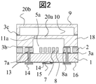
本発明では、前記キャビティ基板は図1では最下面に配置されているが、電極をハンドル基板から引き出す場合は、図2に示す構造を適用することも可能である。
図2の構造は、デバイス基板の構造は図1と同様であるが、電極引き出しをハンドル基板1内に形成した貫通電極13を用いて図2の下面側に引き出している構造である。本発明のキャビティ基板9は最上面に配置されており、キャップ基板18内に形成した通気路11aを介して、デバイス基板2のセンシング空間5aと連通している。また、前記キャップ基板18には大きなセンシング空間5aが形成することも可能である。
図1および図2に示した本発明のキャビティ基板9に作り込むキャビティ空間は、外周部の接合部以外の範囲を空間として利用できる点、深さを基板厚さによって調整できる点から空間体積を大きく形成できる。そのため、圧力変動を抑制することができ、デバイス基板2に形成されたセンシング空間の真空度を安定に保ち、歩留りに優れた物理量センサを提供することができる。
また、空間を有するキャビティ基板9は、センシング部が形成されている基板とは異なる平面に配置されている、センシング部が形成されている複数の基板の製造プロセスとは、別のプロセスで製作することが可能であり、複雑なプロセスとはならず、安価で生産性に優れた物理量センサを提供できる。
本発明の物理量センサの実用的なアセンブル方法では、信号の検出および電気の供給を行うためにLSI等の電極パッドとワイヤボンディングもしくはバンプ等と電気的につなぎこみ、リードフレームおよびコンデンサ等の部品とともに、樹脂材料を適用してモールド成形する。また、圧力センサを適用した場合には、検出部だけ樹脂材料が除かれて構造または検出部だけ通路が形成された構造となっている。
前記のアセンブル方法では、物理量センサの外周部全体に樹脂材料による樹脂応力が印加されるため、物理量センサの構造において変形に弱い部分は好ましくない。
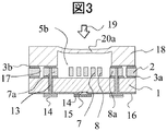
本発明では、前記キャビティ基板はデバイス基板のセンシング空間を保護する役割も存在する。図2の構造では、一般的にキャップ基板18に大きなセンシング空間5aを形成することも可能であるが、本発明のキャビティ基板9が存在しない場合について図3を用いて説明する。
図3は物理量センサ全体を樹脂材料によってモールドを実施した場合を想定した例を示す。この場合、前記のように物理量センサには、樹脂応力19が外力として加わることになる。その時、デバイス基板2のセンシング空間5bの体積は大きいほど、キャップ基板のダイヤフラム部分20aの厚さ薄くなり、ダイヤフラム部分20aは変形することが想定される。
その結果、センシング空間5bの気体の圧力Pは(1)式により、体積Vが減少すると、気体の圧力は増加する。すなわち、センシング空間の圧力ばらつきが大きくなることが予測できる。なお、nは気体の物質量(モル数)、Rは気体定数、Tは気体の熱力学的温度を示す。
PV=nRT ‥‥(1)
PV=nRT ‥‥(1)
そのため、図3に示す構造では、デバイス基板2のセンシング空間5b体積は大きくすることが困難となる。一方、図2に示した本発明では、外部から樹脂応力を外力として加えた場合でも、キャビティ基板のダイヤフラム部分20bは変形することが予測できるが、キャップ基板18のダイヤフラム部分20aは変形することはない。
また、図3の構造と比較して、本発明の図2の構造は、センシング部分5aの体積は、図3のセンシング体積5bと比較して格段に大きいため、ダイヤフラム部分20bが変形した場合でも、(1)式より体積Vが大きい場合には、気体の圧力Pの変化率は小さくなる。
一方、センサエレメントのコストは1枚のシリコンウエハからどのくらいの個数が取得できるかによって変化する。すなわち、センサエレメントを小型化すればするほど、1枚のシリコンウエハから取得するセンサエレメント数が増加し、コストを低減することができる。
微小ガス成分(アウトガス)および接合時に発生するガスによって物理量センサの密閉されたセンシング部の圧力は、目標の圧力と比較して低下するもしくはセンサエレメント間の圧力ばらつきが大きくなる。そのため、前記センシング部の空間体積は広い方が良い。しかし、前記のように低コスト化には小型化が不可欠であり、センサエレメントを大きくすることはできない。本発明ではシリコンウエハの横方向ではなく、縦(積層する厚さ)方向に空間を広げることによって低コストでセンシング部の圧力低下もしくは圧力ばらつきを低減するものである。
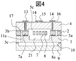
図4に本発明の他の一実施例の断面図を示す。図4の構造では、ハンドル基板1に溝21を形成することによってセンシング部5cの体積を大きくした構造である。
図4の物理量センサの製造プロセスは、はじめにハンドル基板1にフォトリソおよびエッチングを用いて溝21を形成する。その後、熱酸化膜3aを介してデバイス基板2を貼りつける。ここではシリコンの直接接合が好ましい。これは接合時に発生するガスの影響が小さいためである。
シリコンの直接接合は、はじめにシリコンウエハもしくは表面に酸化膜が形成されたシリコンウエハに親水化処理を行い、室温近傍で貼り合わせる。これにより、水素結合によって貼り合わせた2枚のシリコンウエハは結合される。この状態ではまだ、接合強度が弱いため、900度~1100度の温度で加熱処理を行い。それにより、シロキサン結合状態を作り出し強固な結合力が得られる接合方法である。
その後、深掘りのドライエッチング装置によって固定電極7および検出電極8を形成する。次に別プロセスで製作した電極基板4を接合部3bで貼り合わせる。この貼り合わせもシリコンの直接接合を用いることができる。その他に、電気的に導通する金属接合を適用することが可能である。例えば、金とシリコンの共晶接合、金―錫の共晶接合、アルミニウムとゲルマニウムの共晶接合等、各種の金属接合方法を適用できる。その後、通気路11aを深堀のドライエッチング装置によって形成し、最後に別プロセスによって作製したキャビティ基板9を接合部3cで接合する。この場合の接合方法は、前記の金属接合方法よりも融点が低い方法が良い。これは接合部3aおよび3bでの剥離を防止するためである。
本発明では、前記で紹介した物理量センサの各構造に適用するキャビティ基板の材料は、シリコンもしくはガラスを用いることが可能である。より好ましくは複数の基板を、全てシリコン材料で作製することによって物理量センサ構造体の線膨張率が同一となることから信頼性に優れているセンサを提供できる。
一方、パイレックスもしくはテンパックスなどのシリコン材料に線膨張率が近いガラス材料を適用しても良い。この場合の接合法は陽極接合が好ましい。
次にコンバインドセンサの実施例について説明する。
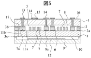
本発明では複数の物理量を測定するセンサを一つの基板に搭載することができる。図5にデバイス基板2には、密閉された2つの空間が形成されている。一方は、空間の圧力雰囲気が真空雰囲気の第一のセンシング空間5であり、もう一方は前記とは異なる圧力雰囲気を有する第二のセンシング空間6である。それぞれのセンシング空間には固定電極7および検出電極8が形成されている。これは数ミクロンのギャップを有して複数の櫛歯が形成されている。キャビティ基板9はデバイス基板と外径が同様の寸法で形成されており、内部にはキャビティ空間10が形成されている。前記空間はハンドル基板1に形成した通気路11aもしくは11bのいずれかの通気路と、デバイス基板の電極基板4は空間の圧力雰囲気が真空のセンシング空間5と連通している。そのため、空間の圧力雰囲気が真空のセンシング空間5の空間体積は大きくなっていることがわかる。
電気的なやり取りは図1で示した方法と同様である。
なお、前記、通気路11bはデバイス基板2に別途設けた空間17とつながっており、デバイス基板内に設けた通路(図示せず)によってセンシング空間5とつながっている。
前記、複数の密閉されたセンシング部には加速度センサ、角速度センサ、圧力センサのうち少なくとも2つ以上を組み合わせることができるため、用途に応じて自由に配置できる。
また、キャビティ基板の外径はコンバインドセンサの外径と同様の寸法で配置することによって、ウエハレベルで積層接合した基板を一括でダイシング加工することが可能であり、生産性にも優れている。
キャビティ基板9のキャビティ空間にゲッタ等の吸着材12を配置することも可能である。吸着材によって内部の圧力をより安定に維持することができるため、長期信頼性にも優れている。なお、吸着材の配置は今までに説明した各実施例にも適用することができる。
前記、吸着材は、薄膜上に形成するのが良い。これは、キャビティ空間の体積を阻害させないためである。吸着材12には500度くらいで活性、すなわち、微量ガス成分の吸着効果を増加させられる。そのため、吸着材を配置した本発明では、各基板の接合方法はそれ以上の温度で接合される方法が良い。
一方、吸着材からごみが発生する場合がある。その場合、通気路11aでは、直接的にセンシング空間5にごみが導入されるおそれがある。そのような場合には、前記通気路11bのように、デバイス基板の内部にごみを捕獲する機構または、ごみがセンシング空間へ進入しにくいノズル機構を配置しても良い。
デバイスが形成されている基板のセンシング部には、多くの可動および検出用の櫛歯および梁がミクロンオーダで形成されている場合が多く、センシング部の空間体積に対して、センシング部の表面積の割合は大きい。その結果、微小ガス成分(アウトガス)が発生する割合が大きくなる。これは表面積の大きさに比例して微小ガス成分が発生する割合が高くなるためである。
一方、キャビティ基板に形成された空間は、内部には構造体はないことから、体積に対する表面積の割合は、センシング部と比較して非常に小さい。そのため、キャビティ基板の空間は微小ガス成分(アウトガス)が発生する割合が小さくなる。
そのため、センシング部とキャビティ基板の空間を通気路によって連通する本発明は圧力の安定に寄与できる。
キャビティ基板に形成された空間体積は同等以上であれば良い。より詳細にはセンシング部の空間体積に対して、少なくとも2倍以上の体積があることが好ましく。空間体積は大きいほど微小ガス成分(アウトガス)および接合における発生ガスの影響を小さくすることが可能となる。これは、前記(1)式より、体積がN倍になると圧力は1/Nとなる。すなわち、体積が大きくなるほど、センシング空間の圧力変動は抑制できる。
一例として櫛歯が形成された構造体のセンシング体積と表面積の割合は、表面積を体積で割った値は約200倍であるが、キャビティ空間における表面積を体積で割った値は約8倍であった。微小ガス成分は表面積に比例して発生するものであると仮定すると、センシング空間で発生する微小ガス成分は、キャビティ空間で発生する微小ガス成分の方が極端に大きいことがわかる。そのため、本発明のキャビティ基板は圧力の安定に効果があると言える。
図5の構造では、キャビティ基板9に形成するキャビティ空間10は、センシング空間6の面積まで広げることが可能であるため、大きな空間を作り出すことができる。
また、キャビティ基板の厚さは自由にコントロールすることができることから、複数基板の全体の厚さを調整することができる。これによって、各種の異なる物理量センサの全体の厚さを一定に保つことができる。そのため、最終的にアセンブルする場合に高さの揃った物理量センサを提供することが可能で、アセンブルに適用する治具等も共通化することが可能となる。
複数の密閉されたセンシング空間の組み合わせでは、加速度センサおよび角速度センサの組合せが好ましい。この構造では加速度センサを大気圧近傍に、角速度センサのセンシング部は100Pa程度の真空で封止する。加速度センサのセンシング部は、大気圧もしくは10000から50000Paくらいの真空度で封止する。角速度センサのセンシング部をキャビティ基板のキャビティ空間とつなぐことによって、角速度センサのセンシング部の真空度を安定に保つことができ、良好な物理量センサを作製できる。
加速度センサ部の圧力雰囲気を10000から50000Paくらいの真空度で封止する理由は、密閉された空間では接合温度によって、前記(1)式の関係から温度が上昇すると、密閉された空間の圧力も上昇する。その場合、接合方法によっては接合部から剥離する場合が想定される。そのため、あらかじめ、減圧状態にすることも必要となる。
前記、加速度センサのセンシング空間には、アルゴン、キセノン、クリプトンなどの分子量が大きな気体を封止することによって、ダンピング効果を高めても良い。
前記コンバインドセンサでは、センシング部の圧力が異なる加速度センサを配置することも可能である。この構造では、高感度の加速度センサおよび低感度の加速度センサを組み合わせることができるため、異なる加速度を同時に計測することが可能となる。
また、圧力センサをコンバインドセンサに搭載して、絶対圧力およびゲージ圧を測定する構造を適用しても良い。
デバイス基板などに形成する通気路は、少なくとも1箇所あれば、本発明の機能を発揮するが、複数本設けても良い。形状は円形が好ましいが、矩形、四角形等、自由に選択することができる。
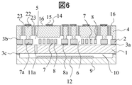
本発明では、他のコンバインドセンサ構造にも適用することができる。図6を用いて説明する。図6の構造は、図5に示した構造において、電極基板4における電極の取り出し方法が異なる。電極引き出しは、ドープされた低抵抗シリコン22を電極として適用している。前記低抵抗シリコンの抵抗値は0.01Ωcm以下が良い。低抵抗シリコン22の電極の周囲は酸化膜16で絶縁されており、その周囲の埋め込み部は導電性がないpoly-Si等の埋め込み材料23で埋め込まれている。
前記の構造ではデバイス基板2に形成された第一のセンシング空間5に角速度センサを、第二のセンシング空間6に加速度センサを配置されている。第一のセンシング空間5では角速度が加わると検出電極8が上下方向に可動し、低抵抗シリコン22の電極とのギャップが変化することによって、静電力が変化し、それを電気信号として検出する構造となっている。そのため、検出電極とその上に配置されている低抵抗シリコンからなる電極とのギャップは数ミクロンと小さい。
また、ハンドル基板1とデバイス基板2にはSOIウエハを適用することができる。
そのため、センシング空間5または6における空間体積は非常に小さくなる。このような適用例においても、本発明のキャビティ基板を付与することによって、キャビティ空間の体積分だけ広げることが可能となる。
そのため、センシング空間5または6における空間体積は非常に小さくなる。このような適用例においても、本発明のキャビティ基板を付与することによって、キャビティ空間の体積分だけ広げることが可能となる。
その結果、センシング空間の圧力変化を吸収でき、圧力ばらつきを抑制できる。
前記の構造では、センシング空間に吸着材を設置するスペースはないが、キャビティ空間10に吸着材12を設置することによっていっそうの圧力ばらつきを抑制できる。
前記の構造では、センシング空間に吸着材を設置するスペースはないが、キャビティ空間10に吸着材12を設置することによっていっそうの圧力ばらつきを抑制できる。
本発明の例を説明したが本発明は上述の例に限定されるものではなく、特許請求の範囲に記載された発明の範囲にて様々な変更が可能であることは、当業者によって容易に理解されよう。
1…固定基板、2…デバイス基板、3…接合部、4…電極基板、5…一番圧力が高真空雰囲気の第一のセンシング空間、6…第二のセンシング空間、7…固定電極、8…検出電極、9…キャビティ基板、10…キャビティ空間、11…通気路、12…吸着材(薄膜ゲッタ)、13…貫通電極、14…金属電極、15…poly-Si、16…酸化膜、17…空間、18…キャップ基板、19…樹脂応力、20…ダイヤフラム、21…溝、22…低抵抗シリコン、23…埋め込み材料
Claims (16)
- 物理量を測定するセンシング部を真空の空間に配置した物理量センサにおいて、
複数の基板を積層してなるセンサ部を有し、
前記センサ部の上面側もしくは下面側に、空間を有するキャビティ基板が接合によって設けられ、
前記センシング部は、前記センサ部に設けられた通気路を介して前記キャビティ基板の空間と連通することを特徴とする物理量センサ。 - 物理量を測定するセンシング部を真空の空間に配置した物理量センサにおいて、
物理量のセンシングを行うセンシング部を有するデバイス基板と、前記デバイス基板を支持するハンドル基板と、前記デバイス基板から電気的導通を行う電極基板と、が積層されており、
前記ハンドル基板に、空間を有するキャビティ基板を接合によって設け、
前記デバイス基板のセンシング部が設けられた空間を前記ハンドル基板に内に形成した通気路を介して前記キャビティ基板の空間に連通することを特徴とする物理量センサ。 - 物理量を測定するセンシング部を複数有し、前記センシング部はそれぞれ密閉された空間に設けられており、前記副巣のセンシング部の各圧力はそれぞれ異なる物理量センサにおいて、
前記センシング部を有するデバイス基板と、前記デバイス基板を支持するハンドル基板と、前記デバイス基板から電気的導通を行う電極基板と、が積層されており、
前記ハンドル基板に、空間を有するキャビティ基板を接合によって設け、
密閉された複数のセンシング部の内、一つのセンシング部が設けられた空間を前記ハンドル基板に内に形成した通気路を介して前記キャビティ基板の空間に連通することを特徴とする物理量センサ。 - 請求項1または2に記載の物理量センサにおいて、
前記センシング部は、加速度センサ、角速度センサ、圧力センサのうちいずれかのセンサであることを特徴とする物理量センサ。 - 請求項3に記載の物理量センサにおいて、
前記複数のセンシング部は、加速度センサ、角速度センサ、圧力センサのうち少なくとも2つ以上を組み合わせたセンサを備えることを特徴とする物理量センサ。 - 請求項1乃至5のいずれかに記載の物理量センサにおいて、
前記キャビティ基板の外径は前記センサの外径と同じであることを特徴とする物理量センサの構造。 - 請求項1乃至6のいずれかに記載の物理量センサにおいて、
前記キャビティ基板にゲッタ等の吸着剤を配置したことを特徴とする物理量センサの構造。 - 請求項1乃至7のいずれかに記載の物理量センサにおいて、
前記デバイス基板のうち圧力が高真空となるセンシング部の空間体積に対して、前記キャビティ基板に形成された空間体積は同等以上であることを特徴とする物理量センサの。 - 請求項1乃至8のいずれかに記載の物理量センサにおいて、
前記ハンドル基板の下面側に空間を形成し、前記キャビティ基板に形成した空間と連通することを特徴とする物理量センサ。 - 請求項1乃至9のいずれかに記載の物理量センサにおいて、
前記キャビティ基板は、シリコンもしくはガラスからなることを特徴とする物理量センサ。 - 請求項10に記載の物理量センサにおいて
前記ハンドル基板および前記デバイス基板は、SOIウエハからなることを特徴とする物理量センサ。 - 請求項3に記載の物理量センサにおいて、
前記複数のセンシング部は、加速度センサと角速度センサからなることを特徴とする物理量センサ。 - 請求項3に記載の物理量センサにおいて、
前記複数のセンシング部は、それぞれセンシング部の内部の圧力が異なる加速度センサからなることを特徴とする物理量センサ。 - 請求項10に記載の物理量センサにおいて、
前記ハンドル基板および前記デバイス基板および前記電極基板をそれぞれシリコン直接接合で封止し、
前記キャビティ基板を金属接合で封止したことを特徴とする物理量センサ。 - 請求項10に記載の物理量センサにおいて、
前記ハンドル基板および前記デバイス基板および前記電極基板をそれぞれシリコン直接接合で封止し、
前記キャビティ基板を陽極接合で封止したことを特徴とする物理量センサ。 - 請求項10に記載の物理量センサにおいて、
前記ハンドル基板および前記デバイス基板をシリコン直接接合で封止し、
前記電極基板を導電性が存在する金属接合で封止したことを特徴とする物理量センサ。
Priority Applications (2)
| Application Number | Priority Date | Filing Date | Title |
|---|---|---|---|
| US14/773,122 US9651408B2 (en) | 2013-03-08 | 2013-12-20 | Structure of physical sensor |
| EP13877142.3A EP2966404A4 (en) | 2013-03-08 | 2013-12-20 | Physical quantity sensor structure |
Applications Claiming Priority (2)
| Application Number | Priority Date | Filing Date | Title |
|---|---|---|---|
| JP2013046092A JP5953252B2 (ja) | 2013-03-08 | 2013-03-08 | 物理量センサの構造 |
| JP2013-046092 | 2013-03-08 |
Publications (1)
| Publication Number | Publication Date |
|---|---|
| WO2014136358A1 true WO2014136358A1 (ja) | 2014-09-12 |
Family
ID=51490898
Family Applications (1)
| Application Number | Title | Priority Date | Filing Date |
|---|---|---|---|
| PCT/JP2013/084183 Ceased WO2014136358A1 (ja) | 2013-03-08 | 2013-12-20 | 物理量センサの構造 |
Country Status (4)
| Country | Link |
|---|---|
| US (1) | US9651408B2 (ja) |
| EP (1) | EP2966404A4 (ja) |
| JP (1) | JP5953252B2 (ja) |
| WO (1) | WO2014136358A1 (ja) |
Families Citing this family (7)
| Publication number | Priority date | Publication date | Assignee | Title |
|---|---|---|---|---|
| JP6750439B2 (ja) * | 2016-09-30 | 2020-09-02 | セイコーエプソン株式会社 | 電子デバイス、電子デバイス装置、電子機器および移動体 |
| US11150092B2 (en) | 2017-01-17 | 2021-10-19 | Panasonic Intellectual Property Management Co., Ltd. | Sensor |
| JP6990997B2 (ja) * | 2017-06-06 | 2022-01-12 | 株式会社日立製作所 | Memsデバイス |
| JP6897703B2 (ja) | 2018-04-24 | 2021-07-07 | 株式会社デンソー | 半導体装置の製造方法 |
| JP7147650B2 (ja) | 2019-03-20 | 2022-10-05 | 株式会社デンソー | 半導体装置およびその製造方法 |
| WO2023021672A1 (ja) | 2021-08-19 | 2023-02-23 | 富士電機株式会社 | センサ装置およびセンサ装置の製造方法 |
| JP2024017550A (ja) * | 2022-07-28 | 2024-02-08 | セイコーエプソン株式会社 | 慣性計測装置、慣性計測装置の製造方法 |
Citations (7)
| Publication number | Priority date | Publication date | Assignee | Title |
|---|---|---|---|---|
| JPH0771965A (ja) * | 1993-07-06 | 1995-03-17 | Tokimec Inc | ジャイロ装置 |
| JPH10206455A (ja) * | 1997-01-21 | 1998-08-07 | Murata Mfg Co Ltd | 減圧封止電子部品の製造方法 |
| JP2002005950A (ja) | 2000-06-23 | 2002-01-09 | Murata Mfg Co Ltd | 複合センサ素子およびその製造方法 |
| WO2006006597A1 (ja) * | 2004-07-12 | 2006-01-19 | Sumitomo Precision Products | 角速度センサ |
| JP2008066521A (ja) | 2006-09-07 | 2008-03-21 | Nissan Motor Co Ltd | パッケージ型電子部品及びパッケージ型電子部品の製造方法 |
| WO2010119573A1 (ja) * | 2009-04-17 | 2010-10-21 | 株式会社日立製作所 | 慣性センサおよびその製造方法 |
| JP2012088319A (ja) * | 2011-11-01 | 2012-05-10 | Denso Corp | 半導体装置およびその製造方法 |
Family Cites Families (10)
| Publication number | Priority date | Publication date | Assignee | Title |
|---|---|---|---|---|
| US5781985A (en) * | 1993-07-06 | 1998-07-21 | Tokimec Inc. | Method of making a gyro apparatus |
| WO2004061983A1 (ja) * | 2002-12-27 | 2004-07-22 | Matsushita Electric Industrial Co., Ltd. | 電子デバイスおよびその製造方法 |
| JP4159895B2 (ja) * | 2003-02-17 | 2008-10-01 | キヤノンアネルバ株式会社 | 静電容量型圧力センサ及びその製造方法 |
| KR100575363B1 (ko) | 2004-04-13 | 2006-05-03 | 재단법인서울대학교산학협력재단 | 미소기계소자의 진공 실장방법 및 이 방법에 의해 진공실장된 미소기계소자 |
| JP5541306B2 (ja) | 2011-05-27 | 2014-07-09 | 株式会社デンソー | 力学量センサ装置およびその製造方法 |
| DE102011085723A1 (de) * | 2011-11-03 | 2013-05-08 | Continental Teves Ag & Co. Ohg | Bauelement und Verfahren zur Herstellung eines Bauelements |
| US9546922B2 (en) * | 2013-08-09 | 2017-01-17 | Continental Automotive Systems, Inc. | Absolute pressure sensor with improved cap bonding boundary |
| US9470593B2 (en) * | 2013-09-12 | 2016-10-18 | Honeywell International Inc. | Media isolated pressure sensor |
| US20150102437A1 (en) * | 2013-10-14 | 2015-04-16 | Freescale Semiconductor, Inc. | Mems sensor device with multi-stimulus sensing and method of fabrication |
| US9463976B2 (en) * | 2014-06-27 | 2016-10-11 | Freescale Semiconductor, Inc. | MEMS fabrication process with two cavities operating at different pressures |
-
2013
- 2013-03-08 JP JP2013046092A patent/JP5953252B2/ja not_active Expired - Fee Related
- 2013-12-20 US US14/773,122 patent/US9651408B2/en not_active Expired - Fee Related
- 2013-12-20 EP EP13877142.3A patent/EP2966404A4/en not_active Withdrawn
- 2013-12-20 WO PCT/JP2013/084183 patent/WO2014136358A1/ja not_active Ceased
Patent Citations (7)
| Publication number | Priority date | Publication date | Assignee | Title |
|---|---|---|---|---|
| JPH0771965A (ja) * | 1993-07-06 | 1995-03-17 | Tokimec Inc | ジャイロ装置 |
| JPH10206455A (ja) * | 1997-01-21 | 1998-08-07 | Murata Mfg Co Ltd | 減圧封止電子部品の製造方法 |
| JP2002005950A (ja) | 2000-06-23 | 2002-01-09 | Murata Mfg Co Ltd | 複合センサ素子およびその製造方法 |
| WO2006006597A1 (ja) * | 2004-07-12 | 2006-01-19 | Sumitomo Precision Products | 角速度センサ |
| JP2008066521A (ja) | 2006-09-07 | 2008-03-21 | Nissan Motor Co Ltd | パッケージ型電子部品及びパッケージ型電子部品の製造方法 |
| WO2010119573A1 (ja) * | 2009-04-17 | 2010-10-21 | 株式会社日立製作所 | 慣性センサおよびその製造方法 |
| JP2012088319A (ja) * | 2011-11-01 | 2012-05-10 | Denso Corp | 半導体装置およびその製造方法 |
Non-Patent Citations (1)
| Title |
|---|
| See also references of EP2966404A4 |
Also Published As
| Publication number | Publication date |
|---|---|
| EP2966404A4 (en) | 2017-03-01 |
| EP2966404A1 (en) | 2016-01-13 |
| JP2014173961A (ja) | 2014-09-22 |
| US9651408B2 (en) | 2017-05-16 |
| US20160003650A1 (en) | 2016-01-07 |
| JP5953252B2 (ja) | 2016-07-20 |
Similar Documents
| Publication | Publication Date | Title |
|---|---|---|
| JP5953252B2 (ja) | 物理量センサの構造 | |
| US8829627B2 (en) | Dynamic quantity sensor device and manufacturing method of the same | |
| JP2015011002A (ja) | 複合センサ | |
| US8186221B2 (en) | Vertically integrated MEMS acceleration transducer | |
| JP5486271B2 (ja) | 加速度センサ、及び加速度センサの製造方法 | |
| US10598689B2 (en) | Out-of plane-accelerometer | |
| EP2414775A1 (en) | Environmentally robust disc resonator gyroscope | |
| JP5732203B2 (ja) | 複合センサの製造方法 | |
| WO2013080238A1 (ja) | 複合センサおよびその製造方法 | |
| CN207265035U (zh) | 一种中心支撑准悬浮式mems芯片封装结构 | |
| CN107512698A (zh) | 一种中心支撑准悬浮式mems芯片封装结构的制作方法 | |
| US20230280366A1 (en) | Physical Quantity Sensor, Inertial Measurement Unit, And Method For Manufacturing Physical Quantity Sensor | |
| CN103420321B (zh) | 混合集成的构件和用于其制造的方法 | |
| CN105388323B (zh) | 振动式传感器装置 | |
| Dao et al. | Simulation and fabrication of a convective gyroscope | |
| EP2873095B1 (en) | Semiconductor secured to substrate via hole in substrate | |
| JP5939168B2 (ja) | 半導体装置 | |
| Schröder et al. | Stress-minimized packaging of inertial sensors using wire bonding | |
| JP6555238B2 (ja) | 力学量センサおよびその製造方法 | |
| JP6643206B2 (ja) | 物理量センサ | |
| JP2018179695A (ja) | 電子装置 | |
| WO2013180696A1 (en) | Device including substrate that absorbs stresses | |
| JPWO2013080238A1 (ja) | 複合センサおよびその製造方法 | |
| WO2018030045A1 (ja) | 力学量センサおよびその製造方法 |
Legal Events
| Date | Code | Title | Description |
|---|---|---|---|
| 121 | Ep: the epo has been informed by wipo that ep was designated in this application |
Ref document number: 13877142 Country of ref document: EP Kind code of ref document: A1 |
|
| WWE | Wipo information: entry into national phase |
Ref document number: 2013877142 Country of ref document: EP |
|
| WWE | Wipo information: entry into national phase |
Ref document number: 14773122 Country of ref document: US |
|
| NENP | Non-entry into the national phase |
Ref country code: DE |