WO2014141398A1 - Procédé de commande pwm et appareil de conversion de puissance l'utilisant - Google Patents
Procédé de commande pwm et appareil de conversion de puissance l'utilisant Download PDFInfo
- Publication number
- WO2014141398A1 WO2014141398A1 PCT/JP2013/056906 JP2013056906W WO2014141398A1 WO 2014141398 A1 WO2014141398 A1 WO 2014141398A1 JP 2013056906 W JP2013056906 W JP 2013056906W WO 2014141398 A1 WO2014141398 A1 WO 2014141398A1
- Authority
- WO
- WIPO (PCT)
- Prior art keywords
- voltage
- phase
- modulation factor
- output
- inverter circuit
- Prior art date
- Legal status (The legal status is an assumption and is not a legal conclusion. Google has not performed a legal analysis and makes no representation as to the accuracy of the status listed.)
- Ceased
Links
Images





Classifications
-
- H—ELECTRICITY
- H02—GENERATION; CONVERSION OR DISTRIBUTION OF ELECTRIC POWER
- H02M—APPARATUS FOR CONVERSION BETWEEN AC AND AC, BETWEEN AC AND DC, OR BETWEEN DC AND DC, AND FOR USE WITH MAINS OR SIMILAR POWER SUPPLY SYSTEMS; CONVERSION OF DC OR AC INPUT POWER INTO SURGE OUTPUT POWER; CONTROL OR REGULATION THEREOF
- H02M7/00—Conversion of AC power input into DC power output; Conversion of DC power input into AC power output
- H02M7/42—Conversion of DC power input into AC power output without possibility of reversal
- H02M7/44—Conversion of DC power input into AC power output without possibility of reversal by static converters
- H02M7/48—Conversion of DC power input into AC power output without possibility of reversal by static converters using discharge tubes with control electrode or semiconductor devices with control electrode
- H02M7/483—Converters with outputs that each can have more than two voltages levels
- H02M7/487—Neutral point clamped inverters
Definitions
- the present invention relates to a PWM (Pulse Width Modulation) control method (control method) of a three-level inverter that converts a DC voltage into a three-phase AC voltage, and a power converter using the same.
- PWM Pulse Width Modulation
- PWM control inverter device power converter using PWM control method
- DC voltage (current) into three-phase AC voltage (current) is motor control, uninterruptible power supply, power conditioner, frequency power converter It is used for such as.
- a triangular wave comparison method sub-harmonic method
- a triangular wave comparison method a triangular wave carrier signal and a sinusoidal voltage command are compared.
- the transistor connected to the high voltage node is turned on, and when the voltage command is low, the low voltage node is set. Turn on the connected transistor.
- a phase voltage corresponding to a three-phase sine wave is obtained.
- the PWM control inverter device there are a two-level inverter and a three-level inverter.
- a two-level inverter which is a typical inverter, inputs a DC voltage + Ed, -Ed to an inverter main circuit, and is positive (+ Ed), negative (-Ed) by a leg circuit composed of two transistors per output phase.
- a three-level inverter inputs a DC voltage + Ed, -Ed and a zero potential obtained by dividing into two by a capacitor to the inverter main circuit, and a leg circuit composed of four transistors per output phase.
- the inverter can output three-stage PWM voltage waveforms of positive (+ Ed), negative ( ⁇ Ed), and 0. Since the change rate of the output voltage due to switching is halved in the 3-level inverter compared to the 2-level inverter, switching is performed by halving the switching voltage of the switch elements constituting the inverter main circuit. Loss can be reduced.
- a two-phase modulation method as a PWM control method for reducing switching loss by stopping transistor switching for a certain period and reducing the number of times the inverter main circuit is switched.
- a zero-phase component signal is added to each phase so that the voltage command given to one phase switching element (switching device) of the three phases becomes the maximum value or the minimum value of the triangular wave carrier. Is fixed to an ON or OFF state for a predetermined period.
- the switching loss of the transistor can be reduced without changing the line voltage of the fundamental wave component.
- the voltage mode is switched every 60 degrees with respect to the phase angle of the output frequency, and control is performed so that each phase is always in an ON or OFF state in order.
- the voltage utilization rate can be increased because the sinusoidal shape of the line voltage is not distorted. It also has features. Note that “3 1/2 ” is the route 3, but is simply simplified as “ ⁇ 3”.
- Patent Document 1 A technique in which a two-phase modulation method is applied to a two-level inverter is disclosed in Patent Document 1. Further, as in the two-phase modulation method, a technique in which a PWM control method for stopping switching of a transistor for a certain period is applied to a three-level inverter is disclosed in Patent Document 2.
- the two-phase modulation method since the two-phase modulation method includes many harmonics in the output phase voltage, it causes harmonic noise. This harmonic also causes a further increase in power loss such as a ground capacitor.
- the modulation factor is high (close to 2 / ⁇ 3), the output voltage jump voltage width and harmonics are small, but when the modulation factor is low, the output voltage jump voltage width, Since the harmonics become large, the adverse effects caused by the zero-phase current and the harmonics become large.
- the present invention solves such problems, and its object is to achieve power loss due to zero-phase voltage (current) of the inverter to which the two-phase modulation method is applied, harmonic noise, and peripheral devices. It is providing the PWM control method which reduces the bad influence on a power converter, and a power converter device using the same.
- the present invention is configured as follows. That is, the PWM control method of the present invention generates a pulse for controlling the switch of the inverter circuit by comparing the first, second and third voltage commands with the carrier triangular wave, and the first, second and third Are obtained by adding a zero-phase signal to the first, second, and third basic sine waves, respectively, and the first, second, and third basic sine waves are 0 to 2 / ⁇ .
- the zero-phase signal is a value obtained by selecting a median value from (1 ⁇ Va), (Va + Vb), and ( ⁇ 1 ⁇ Vb).
- the power conversion device of the present invention includes an inverter circuit composed of a plurality of switching devices that output DC voltage waveforms of three stages of + Ed, 0, and ⁇ Ed using DC voltages + Ed and ⁇ Ed as power sources, And a control circuit for generating a PWM voltage waveform from the output of the inverter circuit, the control circuit being proportional to a predetermined modulation factor M, The amplitude of the frequency component is controlled, and the output voltage of the inverter circuit is set to any one of + Ed, 0, and -Ed with respect to a specific phase angle range of the fundamental frequency component during one period of the fundamental frequency component.
- the output voltage of the inverter circuit is set to + Ed, 0, and ⁇ Ed in the specific phase angle range.
- the modulation factor M is less than 2/3, the output voltage of the inverter circuit is fixed only to a voltage of 0 in the specific phase angle range, and is outside the specific phase angle range.
- the inverter circuit is a three-level output three-level inverter that generates a pulsed voltage waveform with an amplitude Ed at the output of the inverter circuit.
- a PWM control method for reducing power loss due to zero-phase voltage (current) of an inverter to which a two-phase modulation method is applied, harmonic noise, and adverse effects on peripheral devices, and a power converter using the PWM control method are provided. Can be provided.
- FIG. 4A is a diagram when the modulation factor M is 0.9
- FIG. 4B is a graph when the modulation factor M is 0.5.
- FIG. 1 is a block diagram showing a circuit configuration of a power converter (inverter) 10 according to the first embodiment of the present invention.
- the inverter 10 of the present invention includes an inverter main circuit (inverter circuit) 15 and a control circuit 17 that controls the inverter main circuit 15.
- the control circuit 17 includes a basic voltage command generator 11, a voltage command corrector 12, a PWM pulse generator 13, and a gate driver 14. Further, the gate driver 14 includes a plurality of buffer circuits 16.
- a basic voltage command generator 11 receives a modulation factor M and a phase angle ⁇ , and has three-phase sinusoidal basic voltage commands Vu0, Vv0, Vw0 (first, second, and third basic sine waves). ) In accordance with the modulation factor M and the phase angle ⁇ . Details of the modulation factor M, the phase angle ⁇ , and the basic voltage command generator 11 will be described later.
- the voltage command corrector 12 adds the zero-phase signal Vz generated in the voltage command corrector 12 to the basic voltage commands Vu0, Vv0, Vw0, so that the voltage commands Vu, Vv, Vw (first, second, 3rd voltage command) is generated. Details of the voltage command corrector 12 will be described later.
- the PWM pulse generator 13 generates PWM pulse logic signals Pu1 to Pu4, Pv1 to Pv4, Pw1 to Pw4 based on the input voltage commands Vu, Vv, and Vw, and supplies them to the gate driver 14. Details of the PWM pulse generator 13 will be described later.
- the gate driver 14 is composed of a plurality of buffer circuits 16, by which the PWM pulse logic signals (Pu 1 to Pu 4, Pv 1 to Pv 4, Pw 1 to Pw 4) are transferred to the gate drive differential voltage electrical signal ( (Gu1 / Eu1 to Gu4 / Eu4, Gv1 / Ev1 to Gv4 / Ev4, Gw1 / Ew1 to Gw4 / Ew4) and supplied to the inverter main circuit 15. Details of the gate driver 14 and the buffer circuit 16 will be described later.
- the inverter main circuit 15 is a three-level inverter main circuit, and three-stage voltages (Ed, 0, ⁇ Ed) are applied to the output terminals U, V, and W of the inverter main circuit 15 by PWM control using a signal from the PWM pulse generator 13. ) PWM voltage waveform is generated. Details of the inverter main circuit 15 will be described later.
- the basic voltage command generator 11, the voltage command corrector 12, the PWM pulse generator 13, and the gate driver 14 constitute a control circuit 17 for PWM control of the inverter main circuit 15.
- Each circuit of the control circuit 17, or the basic voltage command generator 11, the voltage command corrector 12, the PWM pulse generator 13, and the gate driver 14, which are constituent elements thereof, is constituted by an electronic circuit or a microprocessor. It is manufactured by a software program as a control IC medium.
- the power converter (inverter) 10 using the PWM control method of the two-phase modulation method in which the amplitude of the zero-phase voltage and the zero-phase current is small compared to the prior art is embodied.
- the basic voltage command generator 11 has sinusoidal basic voltage commands Vu0, Vv0, Vw0 (first, second, third) defined according to the modulation factor M and the phase angle ⁇ , as shown in the following equation (1).
- Basic sine wave is generated and output.
- Vu0 M ⁇ sin ( ⁇ )
- Vv0 M ⁇ sin ( ⁇ 120 °)
- Vw0 M ⁇ sin ( ⁇ 240 °)
- the modulation factor M can be arbitrarily changed by a value of 0 to 2 / ⁇ 3.
- the phase angle ⁇ is given with a function that increases in proportion to the time t.
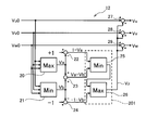
- FIG. 2 is a block diagram showing a circuit configuration of the voltage command corrector 12 provided in the power converter (inverter) 10 according to the first embodiment of the present invention.
- the voltage command corrector 12 includes maximum value selectors (Max) 20 and 26, minimum value selectors (Min) 21 and 25, adders 23, 27, 28 and 29, a subtractor 22, 24.
- the median value selector 201 includes the minimum value selector 25 and the maximum value selector 26.
- the maximum value selector 20 and the minimum value selector 21 receive basic voltage commands Vu0, Vv0, and Vw0.
- the maximum value selector 20 outputs the maximum value Va of the basic voltage commands Vu0, Vv0, Vw0 that change with time.
- the minimum value selector 21 outputs the minimum value Vb of the basic voltage commands Vu0, Vv0, Vw0.
- the subtractor 22 subtracts the maximum value Va from +1 to generate a signal (1-Va).
- the adder 23 adds the maximum value Va and the minimum value Vb to generate a signal (Va + Vb).
- the subtractor 24 subtracts the minimum value Vb from ⁇ 1 to generate a signal of ( ⁇ 1 ⁇ Vb).
- the minimum value selector 25 selects and outputs the smaller one of (1 ⁇ Va) and (Va + Vb).
- the maximum value selector 26 selects and outputs the larger value of the output signal of the minimum value selector 25 and ( ⁇ 1 ⁇ Vb).
- the signal of the maximum value selector 26 is equally applied to each of the sine wave basic voltage commands Vu0, Vv0, and Vw0 constituting the three phases, as will be described below, so that the sine wave basics constituting the three phases are applied. This corresponds to the zero phase component of the voltage commands Vu0, Vv0, Vw0. Therefore, the output signal of the maximum value selector 26 is referred to as a zero phase signal Vz.
- the adders 27, 28, and 29 add the zero-phase signal Vz to the basic voltage commands Vu0, Vv0, and Vw0 (first, second, and third basic sine waves) and respectively add the voltage commands Vu, Vv, and Vw. Output. That is, the voltage commands Vu, Vv, and Vw are shifted from the sinusoidal basic voltage commands Vu0, Vv0, and Vw0 constituting the three phases by the zero-phase signal Vz.
- the voltage commands Vu, Vv, and Vw are different from the sine waveform because they are shifted by the zero-phase signal Vz, but the line voltages (Vu ⁇ Vv), ( Vv ⁇ Vw) and (Vw ⁇ Vu) constitute a three-phase sine wave by canceling the zero-phase signal Vz. Therefore, if the line voltage is used, a three-phase load such as a motor can be driven without any trouble.
- the horizontal axis is the phase angle ⁇ (deg.), And the vertical axis is the value of each signal. However, the vertical axis is normalized by the maximum value of the basic voltage commands Vu0, Vv0, Vw0.
- the modulation factor M is 0.9
- the thick solid line is the zero phase signal (zero phase voltage command) Vz
- the thin broken lines are (1-Va), (Va + Vb), ( ⁇ 1 ⁇ Vb).
- FIG. 3A shows that the zero-phase signal Vz is selected from the median values of (1 ⁇ Va), (Va + Vb), and ( ⁇ 1 ⁇ Vb).
- the modulation factor M is 0.5
- the thick solid line is the zero-phase signal (zero-phase voltage command) Vz
- the thin broken lines are (1-Va) and (-1-Vb).
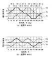
- FIG. 4 is a diagram illustrating waveforms of voltage commands Vu, Vv, and Vw generated by the voltage command corrector 12 included in the power conversion device according to the first embodiment of the present invention.
- (B) is when the modulation factor M is 0.5.
- the horizontal axis is the phase angle ⁇ (deg.), And the vertical axis is the value of each signal. However, the vertical axis is normalized by the maximum value of the voltage commands Vu, Vv, Vw.
- a thick solid line is Vu
- a thin solid line is Vv
- a thin broken line is Vw.
- the condition of the modulation rate at which the voltage commands Vu, Vv, and Vw are fixed at three voltage command values is 2/3 ⁇ M ⁇ 2 / ⁇ 3, and 0 ⁇ M ⁇ 2/3.
- the voltage command value is fixed only at a value of zero.
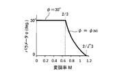
- the parameter ⁇ is a function ⁇ (M) determined depending on the modulation factor M, and is given by the following equation (2).
- ⁇ 30 °
- ⁇ is defined by the frequency method.
- FIG. 5 is a graph showing the relationship between the modulation factor M and the parameter ⁇ in the voltage command corrector provided in the power converter according to the first embodiment of the present invention.
- the horizontal axis of FIG. 5 is the modulation factor M
- the vertical axis is the parameter ⁇ (deg.).
- ⁇ is constant at 30 ° ( ⁇ / 6 radians) when M is smaller than 2/3
- ⁇ is M when M is larger than 2/3.
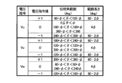
- FIG. 6 shows voltage commands Vu, Vv, Vw in the voltage command corrector provided in the power converter according to the first embodiment of the present invention, and voltage command values ⁇ 1, 0, +1 to which they are fixed. It is a figure showing the relationship which put together the length of the phase angle range used as the conditions where a voltage command is fixed, and the phase angle range. Note that the phase angle range is expressed in the power method (deg.). In FIG.
- the range of the phase angle ⁇ in which the voltage command value is fixed to +1 is 60 ° + ⁇ ⁇ ⁇ 120 ° ⁇ , and the phase angle ⁇ in which the voltage command value is fixed to 0.
- the range is 0 ⁇ ⁇ ⁇ , 180 ° ⁇ ⁇ ⁇ 180 ° + ⁇ , 360 ° ⁇ ⁇ 360 °, and the range of the phase angle ⁇ in which the voltage command value is fixed to ⁇ 1 is 240 ° + ⁇ ⁇ ⁇ 300 ° - ⁇ .
- the lengths of the phase angle ranges in which the voltage command value is fixed to ⁇ 1, 0, ⁇ 1 are 60 ° ⁇ 2 ⁇ , 4 ⁇ , and 60 ° ⁇ 2 ⁇ , respectively.
- (60 ° -2 ⁇ ) + (4 ⁇ ) + (60 ° -2 ⁇ ) 120 °
- the total length of is 120 °.
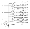
- FIG. 7 is a block diagram showing a circuit configuration of the PWM pulse generator 13 provided in the power conversion device according to the first embodiment of the present invention.
- the PWM pulse generator 13 includes a triangular wave generator 31, a subtractor 32, comparators 33u, 33v, 33w, 34u, 34v, 34w, logic inversion circuits 35u, 35v, 35w, 36u, 36v, 36w, and ON delay.
- the circuit 37 is configured.
- the triangular wave generator 31 generates the carrier triangular wave signal Vcar1 (first carrier triangular wave signal) shown in FIG. 8, and the subtracter subtracts 1 from the value of Vcar1 to thereby generate the carrier triangular wave signal Vcar2 (second carrier triangular wave signal). ).
- the detailed waveforms of the carrier triangular wave signals Vcar1 and Vcar2 will be described later with reference to FIG.
- the comparator 33u compares the voltage command Vu with a triangular wave (carrier triangular wave signal) Vcar1. Further, the comparator 34u compares the voltage command Vu with the triangular wave Vcar2.
- the logic inverting circuit 35u receives the signal from the comparator 33u and outputs the inverted signal.
- the logic inversion circuit 36u receives the signal from the comparator 34u and outputs the inverted signal.
- four types of PWM pulse logic signals Pu1 to Pu4 are generated by combining with the comparators 33u and 34u and the logic inverting circuits 35u and 36u.
- the PWM pulse logic signals Pu1 to Pu4 are output via the ON delay circuit 37. The function of the ON delay circuit 37 will be described later.
- the comparators 33u and 34u usually generate a pulse in any one of Pu1 to Pu4 every period 1 / fc.
- the amplitudes of Vcar1 and Vcar2 of the triangular wave (carrier triangular wave signal) are slightly smaller than 1 (predetermined value)
- pulses are generated in Pu1 to Pu4 only when the voltage command Vu is +1, 0, -1. do not do.
- the predetermined value is a condition that only when the voltage command Vu is +1, 0, ⁇ 1, no pulse is generated in Pu1 to Pu4, and the apex of the triangular wave is close to +1 (or 0, or ⁇ 1).
- a value selected within a range that does not malfunction due to noise or the like is a value selected within a range that does not malfunction due to noise or the like.
- the configurations of the comparators 33v and 34v and the logic inverting circuits 35v and 36v are basically the same as the configurations of the comparators 33u and 34u and the logic inverting circuits 35u and 36u described above, and thus redundant description is omitted. Therefore, a circuit combining the comparators 33v and 34v and the logic inverting circuits 35v and 36v generates the PWM pulse logic signals Pv1 to Pv4 based on the voltage command Vv. Similarly, a circuit combining comparators 33w and 34w and logic inversion circuits 35w and 36w generates PWM pulse logic signals Pw1 to Pw4 based on voltage command Vw.
- the ON delay circuit 37 is a delay circuit for slightly delaying the time when the PWM pulse logic signal becomes H level. However, when the PWM pulse logic signal becomes L level, it is quickly made L level. When the ON delay circuit 37 is at the H level and the L level, a delay time is provided, thereby providing a dead time for the switching operation of the transistor to which the PWM pulse logic signal is supplied, and variations in signal delay, etc. Prevents accidental short circuit.
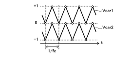
- FIG. 8 is a diagram showing waveforms of carrier triangular wave signals Vcar1 and Vcar2 in the PWM pulse generator provided in the power conversion device according to the first embodiment of the present invention.
- the horizontal axis is the time transition, and the vertical axis is the signal voltage, normalized.
- carrier triangular wave signals Vcar1 and Vcar2 are triangular waves having a frequency of PWM carrier frequency fc and a voltage amplitude slightly smaller than 1 (predetermined value).
- the carrier triangular wave signal Vcar1 sweeps between 0 and +1
- the carrier triangular wave signal Vcar2 sweeps between ⁇ 1 and 0.
- the white circle portion indicates that the solid line of the triangular wave does not reach the broken line slightly. That is, as described above, Vcar1 is a triangular wave that can take a value between 0 and +1 and Vcar2 can take a value between -1 and 0, but does not take a value of +1, 0, or -1.
- the gate driver 14 includes 12 buffer circuits 16 that convert PWM pulse logic signals Pu1 to Pu4, Pv1 to Pv4, and Pw1 to Pw4 into differential voltage electrical signals that are isolated from each other. ing.
- the PWM pulse logic signals (Pu1 to Pu4, Pv1 to Pv4, Pw1 to Pw4) are converted into gate drive differential voltage electrical signals (Gu1 / Eu1 to Gu4 / Eu4, Gv1 / Ev1 to Gv4 / Ev4, Gw1 / Ew1 to Gw4 / Ew4). ) And supplied to the inverter main circuit 15.
- the Pu1 signal is generated as a differential voltage electric signal from the buffer circuit 16 via the buffer circuit 16, and a differential voltage is generated between Gu1 and Eu1 and output as two signals.
- the buffer circuit 16 can isolate output signals from each other by adopting an isolator such as a photocoupler, and has a high gate drive capability by employing a low impedance output circuit such as a push-pull circuit. be able to.
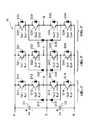
- FIG. 9 is a diagram showing a circuit configuration of the inverter main circuit 15 provided in the power conversion device according to the first embodiment of the present invention.
- the inverter main circuit 15 includes a positive DC power supply P (node P), a negative DC power supply N (node N), and a neutral DC power supply O (node O).
- the node O at the neutral point may be grounded.
- a capacitor C1 is connected between the positive DC power supply P and the neutral DC power supply O, and the voltage of Ed is applied.
- a capacitor C2 is connected between the neutral DC power supply O and the negative DC power supply N, and the voltage of Ed is applied.
- a U-phase leg, a V-phase leg, and a W-phase leg configured by including a transistor and a diode between the positive DC power source P and the negative DC power source N are configured in a parallel configuration corresponding to three phases. Has been.
- the U-phase leg includes transistors Q11 to Q14 and diodes D11 to D16.
- Transistors Q11 to Q14 made of IGBT (Insulated Gate Bipolar Transistor) are connected in series, the collector of the transistor Q11 is connected to a positive DC power supply P, and the emitter of the transistor Q14 is connected to a negative DC power supply N.
- the emitter of the transistor Q12 and the collector of the transistor Q13 are connected to each other and to the output terminal U as a U-phase leg.
- the diodes D11 to D14 are connected in antiparallel to the transistors Q11 to Q14, respectively.
- the anode of the diode D15 is connected to the DC power source O at the neutral point, and the cathode is connected to the connection point between the emitter of the transistor Q11 and the collector of the transistor Q12.
- the cathode of the diode D16 is connected to a neutral direct current power source O, and the anode is connected to the connection point between the emitter of the transistor Q13 and the collector of the transistor Q14.
- Gu1 and Eu1 are applied as a differential voltage electrical signal (Gu1 / Eu1) from the gate driver 14 to the gate and emitter of the transistor Q11 formed of an IGBT, respectively. That is, a signal is applied as a voltage difference between the gate and the emitter.
- Gu2 and Eu2 are applied to the gate and emitter of the transistor Q12 as the differential voltage electrical signal (Gu2 / Eu2) from the gate driver 14, respectively.
- Gu3 and Eu3 are applied to the gate and emitter of the transistor Q13 as differential voltage electrical signals (Gu3 / Eu3) from the gate driver 14, respectively.
- Gu4 and Eu4 are applied to the gate and emitter of the transistor Q14 as differential voltage electrical signals (Gu4 / Eu4) from the gate driver 14, respectively. From the above, the U-phase leg is configured.
- the V phase includes transistors Q21 to Q24 and diodes D21 to D26, and is configured to correspond to the U phase transistors Q11 to Q14 and the diodes D11 to D16, respectively.
- the transistors Q21 to Q24 have the same relationship as that of the U-phase transistors Q11 to Q14 in the differential voltage electrical signals (Gv1 / Ev1), (Gv2 / Ev2), (Gv3 / Ev3), and (Gv4 / Ev4), respectively. It is connected.
- the W phase includes transistors Q31 to Q34 and diodes D31 to D36, and is configured to correspond to the U phase transistors Q11 to Q14 and the diodes D11 to D16, respectively.
- the transistors Q31 to Q34 have the same relationship between the differential voltage electrical signals (Gw1 / Ew1), (Gw2 / Ew2), (Gw3 / Ew3), and (Gw4 / Ew4) as the U-phase transistors Q11 to Q14, respectively. It is connected.
- the DC positive voltage + Ed is applied from the node P and the DC negative voltage -Ed is applied from the node N to each of the U-phase, V-phase, and W-phase legs. Further, a zero voltage (0 potential) is applied from the node O. As described above, the capacitors C1 and C2 are connected between the node PO and the node ON to hold the DC voltage Ed between the nodes.
- each of the U-phase, V-phase, and W-phase legs converts the PWM pulse logic signals Pu1 to Pu4, Pv1 to Pv4, and Pw1 to Pw4 of the PWM pulse generator into a differential voltage electrical signal (Gu1 / Eu1 to (Gu4 / Eu4, Gv1 / Ev1 to Gv4 / Ev4, Gw1 / Ew1 to Gw4 / Ew4) are controlled by the signal so that the inverter main circuit 15 converts the DC voltage (power) into the three-phase AC voltage (power). Fulfills the function of converting to
- the transistors have a silicon IGBT or a silicon MOSFET (Metal-Oxide-) as a switch device (switching device) for ease of turn-on / turn-off control.
- Semiconductor Field-Effect Transistor is preferably used.
- a silicon PiN diode or a silicon Schottky barrier diode as the diodes (D11 to D16, D21 to D26, D31 to D36).
- a wide gap device wide gap power device including a semiconductor having a larger band gap than silicon instead of the silicon device.
- a SiC (Silicon Carbide) device can be applied.
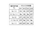
- FIG. 10 is a diagram showing the relationship between the transistors Q11 to Q14 constituting the U-phase leg and the voltage command Vu in the inverter main circuit provided in the power conversion device according to the first embodiment of the present invention.
- the transistors Q11 to Q14 constituting the U-phase leg perform a switching operation according to the voltage command Vu.
- “ON” represents an ON state
- “OFF” represents an OFF state
- “SW” represents a switching state (a repeated state of ON and OFF).
- the transistor Q11 and the transistor Q13 perform a switching operation.
- the transistor Q12 and the transistor Q14 perform a switching operation.
- the transistors Q11 to Q14 are fixed to either ON or OFF, and no switching operation is performed. Therefore, when the voltage command Vu is +1, 0, ⁇ 1, no switching loss occurs in the U-phase leg.
- the voltage commands Vv, Vw are +1, 0, ⁇ 1, respectively, no switching loss occurs in the V-phase leg and the W-phase leg.
- the power conversion device (inverter) 10 reduces switching loss (power consumption), loss due to zero-phase current, and high-frequency noise.
- FIG. 11 is a diagram illustrating a voltage waveform output to the output terminal U of the U-phase leg in the inverter main circuit provided in the power conversion device according to the first embodiment of the present invention.
- (B) is a voltage waveform when the modulation factor M is 0.5.
- the horizontal axis represents the phase angle ⁇ (deg.)
- the vertical axis represents the output voltage.
- the carrier frequency fc used for PWM control is set to 100 times the fundamental frequency f1 constituting a three-phase AC sine wave.
- phase angle is other than the above, a PWM waveform having an amplitude Ed is output to the output terminal U.
- the above applies not only when the modulation factor M is 0.9, but also when the modulation factor 2/3 ⁇ M ⁇ 2 / ⁇ 3.
- ⁇ is the parameter ⁇ described above.
- FIGS. 11 (a) and 11 (b) show that the switching operation of the U-phase leg stops in the range of the phase angle length of 120 °, that is, a period of 1/3 of the whole. Further, for the same reason, the switching operation of the U-phase leg is stopped in the 1/3 overall period for the V-phase leg and the W-phase leg.
- the output of the inverter main circuit 15 is also the output of the power converter device (inverter) 10 of this invention. Therefore, it is also a characteristic of the power conversion device (inverter) 10.
- FIG. 12 is a diagram illustrating a frequency spectrum of a voltage waveform output to the output terminal U of the inverter main circuit 15 provided in the power conversion device according to the first embodiment of the present invention.
- (B) is a frequency spectrum when the modulation factor M is 0.5.
- the horizontal axis represents the harmonic order n, and the vertical axis represents the amplitude value Vn / Ed of the nth-order frequency component Vn.
- the carrier frequency fc is set to 99 times the basic frequency f1.
- V1 is a component of the fundamental frequency f1
- its amplitude value V1 / Ed is 0.90 in FIG. 12A, which is the same value as the modulation factor (0.9).
- FIG. 12B it is 0.50, which is the same value as the modulation rate (0.5).
- V99 is a component of the carrier frequency fc
- its amplitude value V99 / Ed is 0.32 in FIG. 12A and 0.30 in FIG.
- the third-order component V3 is 0.14 in FIG. 12A and 0.21 in FIG.
- FIG. 13 shows the frequency spectrum of the voltage waveform of the output of the three-level inverter to which the control characteristic two-phase modulation method shown in FIG. 19 is applied as a comparative example. And it compares with the frequency spectrum of the voltage waveform of the output of the inverter 10 of this invention mentioned above in FIG.
- the inverter 10 of the present invention is also a three-level inverter to which the two-phase modulation method is applied.
- FIG. 13 is a diagram illustrating a frequency spectrum of a voltage waveform output from a three-level inverter to which a two-phase modulation method of a comparative example described later is applied.
- FIG. ) Is a frequency spectrum when the modulation factor M is 0.5.
- the horizontal axis represents the harmonic order n, and the vertical axis represents the amplitude value Vn / Ed of the nth-order frequency component Vn.
- the carrier frequency fc is set to 99 times the basic frequency f1.
- V1 is a component of the fundamental frequency f1
- its amplitude value V1 / Ed is 0.90 in FIG. 13A, which is the same value as the modulation factor (0.9). .
- V99 is a component of the carrier frequency fc, and its amplitude value V99 / Ed is 0.30 in FIG. 13A and 0.31 in FIG.
- the third harmonic component V3 is 0.16 in FIG. 13A and 0.66 in FIG.
- V9 of the 9th harmonic component and V15 of the 15th harmonic component appear at conspicuous levels.
- FIG. 12 and FIG. 13 which are inverters of the present invention and the comparative example. Comparing FIG. 12 and FIG. 13, most amplitude values of the frequency component Vn of the voltage waveform output to the output terminal U of the first embodiment of the present invention are smaller than that of the two-phase modulation method of the comparative example. ing. In particular, this tendency becomes stronger as the modulation factor M is smaller.
- the amplitude values of higher harmonic components V9, V15, etc. are more significant than the third harmonic component V3.
- these are almost eliminated.
- the inverter using the PWM control method of the present invention can suppress the harmonic component contained in the output voltage waveform to be smaller than that of the inverter using the two-phase modulation method of the comparative example. This tendency is particularly remarkable when the modulation rate is small.
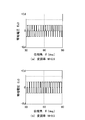
- FIG. 14 is a diagram illustrating a waveform of the zero-phase voltage Ez3 included in the output voltage of the power conversion device (inverter) 10 or the inverter main circuit 15 according to the first embodiment of the present invention.
- the modulation factor M is 0.9
- (b) is a waveform when the modulation factor M is 0.5.
- the vertical axis represents the zero-phase voltage Ez3
- the horizontal axis represents the phase angle ⁇
- the phase angle ⁇ 0 ° to 360 °, and the range of 30 ° to 90 °.
- 14A and 14B show that the amplitude of the zero-phase voltage Ez3 generated by the inverter 10 is within ⁇ 1/3 of the DC voltage Ed. Note that the characteristics of FIG. 14 will be further described while comparing the characteristics of the comparative example shown in FIG.
- FIG. 15 is a diagram showing a waveform of the zero-phase voltage Ez2 included in the output voltage of the three-level inverter using the two-phase modulation method of the comparative example described later.
- FIG. 15A shows a modulation factor M of 0.9.
- (B) is a waveform when the modulation factor M is 0.5.
- the vertical axis represents the zero-phase voltage Ez2
- the horizontal axis represents the phase angle ⁇
- the phase angle ⁇ 0 ° to 360 °
- the range of 30 ° to 90 ° is included. Extracted and shown.
- the inverter of the first embodiment of the present invention corresponds to the waveform of the voltage command value of FIG. 4, and the waveform of FIG. 15 of the inverter of the comparative example is the voltage command of FIG. Corresponds to the value waveform. That is, selecting the waveform of the voltage command value of the inverter of the PWM control method of the present invention as shown in FIG. 4 reduces the zero-phase current and brings about the above effect.
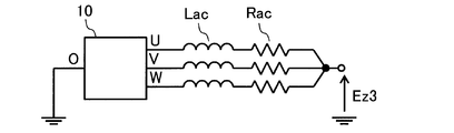
- FIG. 16 is a diagram showing a measurement circuit for the zero-phase voltage Ez3 of the power converter (inverter) 10 according to the first embodiment of the present invention and the zero-phase voltage Ez2 of the comparative example.
- the same resistance as the reactor Lac having the same reactor value is applied to the output terminals U, V, and W of the inverter (10) with the node O of the inverter 10 of the first embodiment of the present invention or the inverter of the comparative example as the ground potential.
- a series circuit of value resistors Rac is connected to each other, and a ground voltage of a node at a portion where one ends of the resistors Rac are connected to each other is observed. With this measurement, the zero-phase voltage Ez (Ez3, Ez2) can be observed.
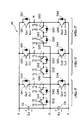
- FIG. 17 is a diagram showing a circuit configuration of the inverter main circuit 45 provided in the power conversion device according to the second embodiment of the present invention.
- the inverter main circuit 45 includes a positive DC power supply P (node P), a negative DC power supply N (node N), and a neutral DC power supply O (node O).
- a capacitor C3 is connected between the positive DC power supply P and the neutral DC power supply O, and the voltage of Ed is applied.
- a capacitor C4 is connected between the neutral DC power supply O and the negative DC power supply N, and the voltage of Ed is applied.
- a U-phase leg, a V-phase leg, and a W-phase leg configured by including a transistor and a diode between the positive DC power source P and the negative DC power source N are configured in a parallel configuration corresponding to three phases. Has been.
- the U-phase leg includes transistors Q41 to Q44 and diodes D41 to D44.
- An IGBT transistor Q41 and a transistor Q44 are connected in series, a collector of the transistor Q41 is connected to a positive DC power supply P (node P), and an emitter of the transistor Q44 is connected to a negative DC power supply N (node N). Yes.
- the emitter of the transistor Q41 and the collector of the transistor Q44 are connected to each other and to the output terminal U as a U-phase leg.
- the transistor Q42 and the transistor Q43 are connected in series via each other's collector, the emitter of the transistor Q42 is connected to the node O, and the emitter of the transistor Q43 is connected to the output terminal U.
- the diodes D41 to D44 are connected in antiparallel to the transistors Q41 to Q44, respectively.
- Gu1 and Eu1 are applied to the gate and emitter of the transistor Q41 formed of IGBT as a differential voltage electrical signal (Gu1 / Eu1) from the gate driver 14, respectively.
- Gu2 and Eu2 are applied to the gate and emitter of the transistor Q42 as differential voltage electrical signals (Gu2 / Eu2) from the gate driver 14, respectively.
- Gu3 and Eu3 are applied to the gate and emitter of the transistor Q43 as differential voltage electrical signals (Gu3 / Eu3) from the gate driver 14, respectively.
- Gu4 and Eu4 are applied to the gate and emitter of the transistor Q44 as differential voltage electrical signals (Gu4 / Eu4) from the gate driver 14, respectively. From the above, the U-phase leg is configured.
- connection configuration of the transistor Q42 and the transistor Q43 is different from the configuration of the connection of the transistor Q12 and the transistor Q13 of the inverter main circuit 15 (FIG. 9) of the first embodiment, but the output terminal as a U-phase leg. From U, a substantially similar output waveform is output.
- the V phase includes transistors Q51 to Q54 and diodes D51 to D54, and is configured to correspond to the U phase transistors Q41 to Q44 and the diodes D41 to D44, respectively.
- the differential voltage electrical signals Gv1 / Ev1), (Gv2 / Ev2), (Gv3 / Ev3), and (Gv4 / Ev4) are respectively related to the transistors Q51 to Q54 in the same relationship as the U-phase transistors Q41 to Q44. Connected with.
- the W phase includes transistors Q61 to Q64 and diodes D61 to D64, and is configured to correspond to the U phase transistors Q41 to Q44 and the diodes D41 to D44, respectively.
- the differential voltage electrical signals (Gw1 / Ew1), (Gw2 / Ew2), (Gw3 / Ew3), and (Gw4 / Ew4) are respectively connected to the transistors Q61 to Q64 in the same relationship as the U-phase transistors Q11 to Q14. Connected with.
- the DC positive voltage + Ed is applied from the node P and the DC negative voltage -Ed is applied from the node N to the U-phase, V-phase, and W-phase legs, and the zero voltage (0 potential) is applied from the node O. ) Is given.
- the capacitors C3 and C4 are connected between the node PO and the node ON to hold the DC voltage Ed between the nodes.
- each of the U-phase, V-phase, and W-phase legs converts the PWM pulse logic signals Pu1 to Pu4, Pv1 to Pv4, and Pw1 to Pw4 of the PWM pulse generator into a differential voltage electrical signal (Gu1 / Eu1 to (Gu4 / Eu4, Gv1 / Ev1 to Gv4 / Ev4, Gw1 / Ew1 to Gw4 / Ew4) are controlled by the signal so that the inverter main circuit 45 converts the DC voltage (power) into the three-phase AC voltage (power). Fulfills the function of converting to
- the number of diode elements can be reduced by six compared to the circuit of FIG.
- the number of series-connected transistors and diodes between the output terminals U, V, and W, and the nodes P and N is reduced from 2 to 1, these elements are required to have double withstand voltage.
- a wide gap device wide gap power device
- a semiconductor element having a larger band gap than silicon instead of the silicon device.
- a SiC device can be applied.
- a silicon IGBT or a silicon MOSFET for the transistor used in the circuit of FIG. 17 because of easy control of turn-on / turn-off.
- the diode a silicon PiN diode or a silicon Schottky barrier diode is used.
- Comparative example As a comparative example, an example in which the voltage command of the two-phase modulation method when the voltage command value is not fixed to 0 is applied to a three-level inverter is shown below.
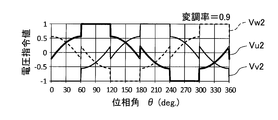
- FIG. 18 is a diagram illustrating an example of the voltage command of the two-phase modulation method of the comparative example (when the voltage command value is not fixed to 0).
- the vertical axis represents the (normalized) voltage command value, and the horizontal axis represents the phase angle.
- the voltage commands Vu2, Vv2, and Vw2 are generated by adding a zero-phase signal to the basic sine wave signal.
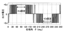
- the waveforms (Vu2, Vv2, Vw2) in FIG. 18 a phase angle range in which the voltage command value is fixed at +1 and ⁇ 1 is formed.
- the voltage command Vu2 is fixed to +1 at a phase angle of 60 ° to 120 °, and is fixed to ⁇ 1 at a phase angle of 240 ° to 300 °. Note that the range in which the voltage command value is fixed at 0 as shown in FIG. 4 of the present invention does not exist in FIG. 18 of the comparative example.
- the PWM voltage waveform (only one phase is shown) shown in FIG. 19 can be output.
- FIG. 19 is a diagram illustrating a PWM voltage waveform (U phase) obtained by applying the voltage command of the two-phase modulation method of the comparative example to the three-level inverter.
- the vertical axis represents the output voltage
- the horizontal axis represents the phase angle.
- the PWM voltage waveform shown in FIG. 19 is obtained by comparing the voltage command value shown in FIG. 18 with two carrier triangular waves having amplitudes of 0 to +1 and ⁇ 1 to 0 and a PWM signal obtained by a comparator. It is obtained by switching the transistor.
- FIG. 19 is a diagram illustrating a PWM voltage waveform (U phase) obtained by applying the voltage command of the two-phase modulation method of the comparative example to the three-level inverter.
- the vertical axis represents the output voltage
- the horizontal axis represents the phase angle.
- the PWM voltage waveform shown in FIG. 19 is obtained by comparing the voltage command value shown in FIG. 18 with two carrier triangular waves having ampli
- the output voltage waveform (PWM voltage waveform) is fixed to + Ed at a phase angle of 60 ° to 120 °, and is fixed to ⁇ Ed at a phase angle of 240 ° to 300 °. Therefore, the switching operation of the three-level inverter can be stopped at 120 ° out of the total phase angle 360 °. Therefore, in each switch element constituting the inverter, the number of times of switching can be reduced to 2/3, and the switching loss can be reduced.
- Patent Document 1 and Patent Document 2 describe a two-phase modulation method and a PWM control method for stopping switching of a transistor for a certain period as in the case of two-phase modulation. Note that the two-phase modulation method does not distort the sinusoidal shape of the line voltage even if the modulation rate is increased to 2 / ⁇ 3, which is larger than 1, so that the voltage utilization rate can be increased. I have. However, the two-phase modulation method of the comparative example shown in FIGS. 18 and 19 is a method of fixing the voltage command value to +1 or ⁇ 1 but not fixing it to 0.
- the voltage command value is fixed to 0 within a predetermined phase angle range.
- the present invention uses a zero-phase voltage command that reduces the generation of harmonics, so that there is little zero-phase current, and there is an effect of reducing power consumption and noise due to harmonics and zero-phase current. This is particularly noticeable when the modulation rate is small.
- Control circuit 17 ⁇ Control circuit 17
- the control circuit 17 that controls the inverter main circuit 15 has been described as being configured with the basic voltage command generator 11, the voltage command corrector 12, the PWM pulse generator 13, and the gate driver 14. It is not limited.
- the gate driver 14 may be included in the PWM pulse generator 13.
- the basic voltage command generator 11 and the voltage command corrector 12 may be integrated.
- the basic voltage command generator 11, the voltage command corrector 12, and the PWM pulse generator 13 may be configured by individual hardware circuits, MPU (Micro-Processing Unit), A configuration may be adopted in which control is performed collectively by a software program using a control IC such as a CPU (Central Processing Unit) as a medium.
- MPU Micro-Processing Unit
- the transistor is described as an IGBT, and the possibility of using a MOSFET instead has been described.
- the transistor basically needs to be a switching element, it is limited to an IGBT or a MOSFET.
- BJT Bipolar junction transistor
- BiCMOS Bipolar Complementary Metal Oxide Semiconductor
- SiC SiC was mentioned as a wide gap device, it is not limited to this.
- a semiconductor device such as GaN (gallium nitride) or Ga 2 O 3 (gallium oxide) may be used.
- diode 9 and 17 it has been described that the diodes (D11 to D14, D21 to D24, D31 to D34, D41 to D44, D51 to D54, D61 to D64) are connected in reverse parallel to the transistor (IGBT).
- IGBT transistor
- a parasitic diode incorporated in a transistor (IGBT, MOSFET) may be used without being added as an element.
Landscapes
- Engineering & Computer Science (AREA)
- Power Engineering (AREA)
- Inverter Devices (AREA)
Abstract
L'invention concerne un circuit inverseur dans lequel une pluralité de dispositifs de commutation sont conçus pour utiliser une tension de courant continu (+Ed, -Ed) comme source de puissance, et pour générer la forme d'onde de tension PWM à trois niveaux (+Ed, 0 et -Ed) ; un circuit de commande pour activer ou désactiver la pluralité des dispositifs de commutation et pour générer la forme d'onde de tension PWM sur la base de la sortie du circuit inverseur. Le circuit de commande régule l'amplitude de la composante de fréquence fondamentale de la forme d'onde de tension PWM proportionnellement à un facteur de modulation prescrit (M) ; au cours d'un cycle de la composante de fréquence fondamentale, établit la tension de sortie du circuit de l'onduleur à +Ed, 0 ou -Ed par rapport à une portée d'angle de phase spécifiée pour la composante de fréquence fondamentale ; corrige la tension de sortie du circuit inverseur à toutes les tensions +Ed, 0 et -Ed dans la portée d'angle de phase spécifiée lorsque la modulation (M) est de 2/3 ou supérieure ; établit la tension de sortie du circuit inverseur à une tension de 0 dans la portée d'angle de phase spécifiée lorsque la modulation (M) est inférieure à 2/3.
Priority Applications (1)
| Application Number | Priority Date | Filing Date | Title |
|---|---|---|---|
| PCT/JP2013/056906 WO2014141398A1 (fr) | 2013-03-13 | 2013-03-13 | Procédé de commande pwm et appareil de conversion de puissance l'utilisant |
Applications Claiming Priority (1)
| Application Number | Priority Date | Filing Date | Title |
|---|---|---|---|
| PCT/JP2013/056906 WO2014141398A1 (fr) | 2013-03-13 | 2013-03-13 | Procédé de commande pwm et appareil de conversion de puissance l'utilisant |
Publications (1)
| Publication Number | Publication Date |
|---|---|
| WO2014141398A1 true WO2014141398A1 (fr) | 2014-09-18 |
Family
ID=51536100
Family Applications (1)
| Application Number | Title | Priority Date | Filing Date |
|---|---|---|---|
| PCT/JP2013/056906 Ceased WO2014141398A1 (fr) | 2013-03-13 | 2013-03-13 | Procédé de commande pwm et appareil de conversion de puissance l'utilisant |
Country Status (1)
| Country | Link |
|---|---|
| WO (1) | WO2014141398A1 (fr) |
Cited By (3)
| Publication number | Priority date | Publication date | Assignee | Title |
|---|---|---|---|---|
| WO2016092603A1 (fr) * | 2014-12-08 | 2016-06-16 | 株式会社日立産機システム | Dispositif de transformation d'énergie et son procédé de commande |
| EP3382870A1 (fr) * | 2017-03-31 | 2018-10-03 | Mitsubishi Heavy Industries Thermal Systems, Ltd. | Appareil onduleur, conditionneur d'air, procédé de commande d'appareil onduleur et programme |
| JP6585872B1 (ja) * | 2018-10-30 | 2019-10-02 | 東芝三菱電機産業システム株式会社 | 電力変換装置 |
Citations (8)
| Publication number | Priority date | Publication date | Assignee | Title |
|---|---|---|---|---|
| JPH0690564A (ja) * | 1991-08-21 | 1994-03-29 | Hitachi Ltd | 直列多重インバ−タの制御装置及び方法 |
| JPH1052062A (ja) * | 1996-07-31 | 1998-02-20 | Fuji Electric Co Ltd | 3レベルインバータの制御装置 |
| JP2002238266A (ja) * | 2002-02-20 | 2002-08-23 | Hitachi Ltd | パルス幅変調方式インバータの制御装置 |
| JP2005045846A (ja) * | 2003-07-22 | 2005-02-17 | Hitachi Ltd | 電力変換装置 |
| JP2006254671A (ja) * | 2005-03-14 | 2006-09-21 | Denso Corp | 三相電圧型インバータ装置 |
| JP2007282484A (ja) * | 2007-03-26 | 2007-10-25 | Hitachi Ltd | 3レベル電力変換装置 |
| WO2010119929A1 (fr) * | 2009-04-16 | 2010-10-21 | 株式会社明電舎 | Procédé de commande d'un appareil de conversion de puissance |
| JP2011160529A (ja) * | 2010-01-29 | 2011-08-18 | Aisin Aw Co Ltd | 回転電機制御装置 |
-
2013
- 2013-03-13 WO PCT/JP2013/056906 patent/WO2014141398A1/fr not_active Ceased
Patent Citations (8)
| Publication number | Priority date | Publication date | Assignee | Title |
|---|---|---|---|---|
| JPH0690564A (ja) * | 1991-08-21 | 1994-03-29 | Hitachi Ltd | 直列多重インバ−タの制御装置及び方法 |
| JPH1052062A (ja) * | 1996-07-31 | 1998-02-20 | Fuji Electric Co Ltd | 3レベルインバータの制御装置 |
| JP2002238266A (ja) * | 2002-02-20 | 2002-08-23 | Hitachi Ltd | パルス幅変調方式インバータの制御装置 |
| JP2005045846A (ja) * | 2003-07-22 | 2005-02-17 | Hitachi Ltd | 電力変換装置 |
| JP2006254671A (ja) * | 2005-03-14 | 2006-09-21 | Denso Corp | 三相電圧型インバータ装置 |
| JP2007282484A (ja) * | 2007-03-26 | 2007-10-25 | Hitachi Ltd | 3レベル電力変換装置 |
| WO2010119929A1 (fr) * | 2009-04-16 | 2010-10-21 | 株式会社明電舎 | Procédé de commande d'un appareil de conversion de puissance |
| JP2011160529A (ja) * | 2010-01-29 | 2011-08-18 | Aisin Aw Co Ltd | 回転電機制御装置 |
Cited By (7)
| Publication number | Priority date | Publication date | Assignee | Title |
|---|---|---|---|---|
| WO2016092603A1 (fr) * | 2014-12-08 | 2016-06-16 | 株式会社日立産機システム | Dispositif de transformation d'énergie et son procédé de commande |
| JPWO2016092603A1 (ja) * | 2014-12-08 | 2017-06-08 | 株式会社日立産機システム | 電力変換装置および電力変換装置の制御方法 |
| CN107112936A (zh) * | 2014-12-08 | 2017-08-29 | 株式会社日立产机系统 | 电力转换装置和电力转换装置的控制方法 |
| CN107112936B (zh) * | 2014-12-08 | 2019-08-16 | 株式会社日立产机系统 | 电力转换装置和电力转换装置的控制方法 |
| EP3382870A1 (fr) * | 2017-03-31 | 2018-10-03 | Mitsubishi Heavy Industries Thermal Systems, Ltd. | Appareil onduleur, conditionneur d'air, procédé de commande d'appareil onduleur et programme |
| JP6585872B1 (ja) * | 2018-10-30 | 2019-10-02 | 東芝三菱電機産業システム株式会社 | 電力変換装置 |
| WO2020089990A1 (fr) * | 2018-10-30 | 2020-05-07 | 東芝三菱電機産業システム株式会社 | Dispositif de conversion de puissance |
Similar Documents
| Publication | Publication Date | Title |
|---|---|---|
| CN102075106B (zh) | 多电平转换器操作 | |
| Chen et al. | Review on pulse‐width modulation strategies for common‐mode voltage reduction in three‐phase voltage‐source inverters | |
| US9787217B2 (en) | Power conversion circuit and power conversion system | |
| Holtz et al. | A space vector modulator for the high-switching frequency control of three-level SiC inverters | |
| US10581342B2 (en) | Three-level two-stage decoupled active NPC converter | |
| Ooi et al. | Five-level multiple-pole PWM AC–AC converters with reduced components count | |
| Hakami et al. | Dual-carrier-based PWM method for DC-link capacitor lifetime extension in three-level hybrid ANPC inverters | |
| CN111656664B (zh) | 电力转换装置 | |
| JPWO2010146637A1 (ja) | 電力変換装置 | |
| Gang et al. | Neutral-point voltage balancing in three-level inverters using an optimized virtual space vector PWM with reduced commutations | |
| US20120163045A1 (en) | Power converter and method for controlling same | |
| Jeong et al. | Finite control set–model predictive control of H8 inverter considering dead-time effect for PMSM drive systems with reduced conducted common-mode EMI and current distortions | |
| Chattejee et al. | Pulse-width modulation techniques in two-level voltage source inverters-state of the art and future perspectives | |
| Madan et al. | Comparison of two-level and three-level NPC inverter topologies for a PMSM drive for electric vehicle applications | |
| US8947897B2 (en) | Current-source power converting apparatus | |
| Halabi et al. | Integrated voltage vector–based SVPWM for reliability and performance enhancement of five-level HANPC inverters | |
| Saied et al. | On three-phase six-switches voltage source inverter: A 150° conduction mode | |
| WO2014141398A1 (fr) | Procédé de commande pwm et appareil de conversion de puissance l'utilisant | |
| Dewani et al. | A general multilevel polygonal space vector generation scheme with reduced switching for the inverter and harmonic suppression using a switched-capacitive filter for the full modulation range | |
| Wang et al. | A VSFPWM method of three-phase CSI for EMI mitigation based on DC current ripple prediction | |
| Zhang et al. | A New PWM scheme for loss balancing and neutral-point voltage balancing in three-level active NPC converter | |
| JP6305363B2 (ja) | インバータ装置および車両 | |
| KR102597788B1 (ko) | 전력 변환 장치 | |
| Sutikno et al. | An efficient strategy to generate high resolution three-phase pulse width modulation signal based on field programmable gate array | |
| CN106341050A (zh) | 多电平变频器及多电平变频器的控制方法 |
Legal Events
| Date | Code | Title | Description |
|---|---|---|---|
| 121 | Ep: the epo has been informed by wipo that ep was designated in this application |
Ref document number: 13877864 Country of ref document: EP Kind code of ref document: A1 |
|
| NENP | Non-entry into the national phase |
Ref country code: DE |
|
| 122 | Ep: pct application non-entry in european phase |
Ref document number: 13877864 Country of ref document: EP Kind code of ref document: A1 |
|
| NENP | Non-entry into the national phase |
Ref country code: JP |