WO2014148568A1 - Système et procédé permettant de produire des dispositifs d'affichage optique - Google Patents
Système et procédé permettant de produire des dispositifs d'affichage optique Download PDFInfo
- Publication number
- WO2014148568A1 WO2014148568A1 PCT/JP2014/057585 JP2014057585W WO2014148568A1 WO 2014148568 A1 WO2014148568 A1 WO 2014148568A1 JP 2014057585 W JP2014057585 W JP 2014057585W WO 2014148568 A1 WO2014148568 A1 WO 2014148568A1
- Authority
- WO
- WIPO (PCT)
- Prior art keywords
- bonding
- sheet
- optical
- optical member
- optical display
- Prior art date
- Legal status (The legal status is an assumption and is not a legal conclusion. Google has not performed a legal analysis and makes no representation as to the accuracy of the status listed.)
- Ceased
Links
Images




Classifications
-
- G—PHYSICS
- G02—OPTICS
- G02F—OPTICAL DEVICES OR ARRANGEMENTS FOR THE CONTROL OF LIGHT BY MODIFICATION OF THE OPTICAL PROPERTIES OF THE MEDIA OF THE ELEMENTS INVOLVED THEREIN; NON-LINEAR OPTICS; FREQUENCY-CHANGING OF LIGHT; OPTICAL LOGIC ELEMENTS; OPTICAL ANALOGUE/DIGITAL CONVERTERS
- G02F1/00—Devices or arrangements for the control of the intensity, colour, phase, polarisation or direction of light arriving from an independent light source, e.g. switching, gating or modulating; Non-linear optics
- G02F1/01—Devices or arrangements for the control of the intensity, colour, phase, polarisation or direction of light arriving from an independent light source, e.g. switching, gating or modulating; Non-linear optics for the control of the intensity, phase, polarisation or colour
- G02F1/13—Devices or arrangements for the control of the intensity, colour, phase, polarisation or direction of light arriving from an independent light source, e.g. switching, gating or modulating; Non-linear optics for the control of the intensity, phase, polarisation or colour based on liquid crystals, e.g. single liquid crystal display cells
- G02F1/1303—Apparatus specially adapted to the manufacture of LCDs
-
- B—PERFORMING OPERATIONS; TRANSPORTING
- B32—LAYERED PRODUCTS
- B32B—LAYERED PRODUCTS, i.e. PRODUCTS BUILT-UP OF STRATA OF FLAT OR NON-FLAT, e.g. CELLULAR OR HONEYCOMB, FORM
- B32B2457/00—Electrical equipment
- B32B2457/20—Displays, e.g. liquid crystal displays, plasma displays
Definitions
- the present invention relates to a production system and production method for an optical display device such as a liquid crystal display.
- This application claims priority based on Japanese Patent Application No. 2013-058977 filed in Japan on March 21, 2013 and Japanese Patent Application No. 2013-104149 filed in Japan on May 16, 2013. The contents are incorporated here.
- an optical member such as a polarizing plate to be bonded to a liquid crystal panel (optical display component) is formed from a long film into a sheet piece having a size matching the display area of the liquid crystal panel After being cut out, packed and transported to another line, it may be bonded to a liquid crystal panel (see, for example, Patent Document 1).
- the present invention has been made in view of the above circumstances, and provides an optical display device production system and production method capable of enlarging the display area and reducing the size of the device by reducing the frame portion around the display area.
- an optical display device production system in which an optical member is bonded to an optical display component, a plurality of the optical display components conveyed on a line are used.
- the optical member sheet was cut to a length corresponding to the display area while the belt-shaped optical member sheet having a width corresponding to the display area of the optical display component was unwound from the original roll, thereby forming the optical member.
- the bonding apparatus which bonds the said optical member to the said optical display component, and the said bonding apparatus bonds the said optical member bonded and hold
- a head a moving device for relatively moving the bonding head and the optical display component at the time of bonding the optical member, and before pressing the optical member against the optical display component at the time of bonding the optical member
- a driving device for driving so as to tilt along the bonding head to the curvature of the holding surface, the production system of the optical display device having provided.
- Said 1st aspect WHEREIN It further has a control apparatus which controls the said moving apparatus and the said drive apparatus, The said control apparatus is the said holding surface of the said bonding head tilted at the time of the said bonding to the said optical display component.
- feeding-out direction of the said optical member may be sufficient.
- the said 1st aspect WHEREIN The structure which aligns the relative position of the said optical member with respect to the said bonding head to a predetermined reference position may be sufficient.
- the said bonding apparatus cuts the said optical member sheet
- the structure which further has the cut part used as a member, and the peeling part which peels the said optical member from the said separator sheet may be sufficient.
- the said moving apparatus is the structure which moves the said bonding head between the peeling position from the said separator sheet of the said optical member, and the bonding position to the said optical display component of the said optical member. Good.
- the said peeling part peels the said optical member from the said separator sheet
- the structure which moves between the said peeling position and the said bonding position may be sufficient in the state which stuck and hold
- an optical display device production system in which an optical member is bonded to an optical display component, and one of a long side and a short side of a display region of the optical display component. While the belt-shaped optical member sheet having a width wider than the length of one side is unwound from the original roll, the optical member sheet is made longer than the length of one of the long side and the short side of the display region.
- a bonding device for bonding the sheet piece to the optical display component, and a portion of the portion facing the display area from the sheet piece bonded to the optical display component
- a cutting device that cuts off an excess portion arranged on the outside and forms the optical member having a size corresponding to the display area, and the bonding device is attached to and held on an arc-shaped holding surface.
- the sheet piece is A bonding head for bonding to a component, a moving device for relatively moving the bonding head and the optical display component at the time of bonding of the sheet piece, and an optical display of the sheet piece at the time of bonding of the sheet piece.
- the said 2nd aspect further has a control apparatus which controls the said moving apparatus and the said drive apparatus, and the said control apparatus is the said optical display component from the said holding surface of the said bonding head tilted at the time of the said bonding.
- feeding-out direction of the said optical member to a may be sufficient.
- the said 2nd aspect WHEREIN The said bonding apparatus cuts the said optical member sheet
- the optical display in the method for producing an optical display device in which an optical member is bonded to an optical display component, the optical display is applied to a plurality of the optical display components conveyed on a line. After the belt-shaped optical member sheet having a width corresponding to the display area of the part is unwound from the original roll, the optical member sheet is cut to a length corresponding to the display area to obtain the optical member, and then the optical member A bonding step of bonding the optical member to the optical display component, and the bonding step holds the optical member on an arc-shaped holding surface of the bonding head, and holds the optical member on the holding surface.
- the method of producing an optical display device having a driving step of driving the so that, there is provided.
- the optical head in the driving step and the moving step, the optical head is pressed against the optical display component, and the bonding head and the optical display component are moved relative to each other, so A configuration in which torque is generated along a feeding direction of the optical member from the holding surface to the optical display component may be employed.
- the optical member sheet is longer than the length of one of the long side and the short side of the display region.
- a bonding step of bonding the sheet piece to the optical display component, and outside the portion facing the display area from the sheet piece bonded to the optical display component A cutting step of cutting the arranged surplus portion and forming the optical member having a size corresponding to the display area, and the bonding step holds the sheet piece on an arc-shaped holding surface. Holding step; A moving step for relatively moving the bonding head holding the sheet piece on the holding surface and the optical display component, and the bonding head for pressing the sheet piece against the optical display component along the curvature of the holding surface
- the said at the time of bonding A configuration may be adopted in which torque is generated along a feeding direction of the sheet piece from the holding surface to the optical display component.
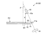
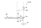
- an optical display device production system in which an optical member is bonded to an optical display component, and any one of a long side and a short side of a display region of the optical display component. While the belt-shaped optical member sheet having a width wider than the length of one side is unwound from the original roll, the optical member sheet is made longer than the length of one of the long side and the short side of the display region.
- a bonding apparatus for bonding the sheet piece to the optical display component, and a bonding surface of the optical display component and the sheet piece on which the sheet piece is bonded
- the detection device for detecting the outer peripheral edge of the sheet, and the excess portion disposed outside the portion corresponding to the bonding surface from the sheet piece bonded to the optical display component, the size corresponding to the bonding surface Cutting device for forming the optical member
- a moving device that relatively moves the head and the optical display component, and the bonding head that presses the sheet piece against the optical display component when the sheet piece is bonded is tilted along the curvature of the holding surface.
- An optical display that cuts the sheet piece along an outer peripheral edge of the bonding surface between the optical display component and the sheet piece detected by the detection device.
- a device production system is provided.
- the “bonding surface between the optical display component and the sheet piece” in the above configuration refers to a surface facing the sheet piece of the optical display component, and “the outer peripheral edge of the bonding surface” specifically refers to In the optical display component, the outer peripheral edge of the substrate on which the sheet piece is bonded is indicated.
- the “part corresponding to the bonding surface” of the sheet piece means that the outer shape of the optical display component (contour shape in plan view) is not less than the size of the display area of the optical display component facing the sheet piece.
- the “size corresponding to the bonding surface” refers to a size not less than the size of the display area of the optical display component and not more than the size of the outer shape (contour shape in plan view) of the optical display component.
- the said 5th aspect WHEREIN It has further the control apparatus which controls the said moving apparatus and the said drive apparatus, and the said control apparatus is the said optical display component from the said holding surface of the said bonding head tilted at the time of the said bonding.
- the driving device and the moving device may be controlled so as to generate a torque along the feeding direction of the sheet piece.
- the said bonding apparatus cuts the said optical member sheet with the separator sheet which unwinds the said optical member sheet with a separator sheet, and cuts the said optical member sheet leaving the said separator sheet, and the said sheet
- the structure which further has the cut part made into a piece, and the peeling part which peels the said sheet piece from the said separator sheet may be sufficient.
- the optical member sheet is longer than the length of one of the long side and the short side of the display region.
- the bonding step of bonding the sheet piece to the optical display component, and the outside of the bonding surface of the optical display component to which the sheet piece is bonded and the sheet piece A detection step for detecting a peripheral edge, and cutting off an excess portion disposed outside the portion corresponding to the bonding surface from the sheet piece bonded to the optical display component, and having a size corresponding to the bonding surface.
- a cutting step for forming the optical member Including a holding step of holding and holding the sheet piece on an arc-shaped holding surface, and a movement of relatively moving the bonding head holding the sheet piece on the holding surface and the optical display component.
- a driving step for driving the bonding head that presses the sheet piece against the optical display component so as to tilt along the curvature of the holding surface and in the cutting step, the detection step A method for producing an optical display device is provided that cuts the sheet piece along an outer peripheral edge of the bonding surface between the detected optical display component and the sheet piece.
- the bonding head and the optical display component are moved relative to each other at the time of bonding.
- a configuration may be adopted in which torque is generated along a feeding direction of the sheet piece from the holding surface to the optical display component.
- the dimensional variation and bonding variation of an optical member can be suppressed, the frame part around a display area can be reduced, and an enlargement of a display area and size reduction of an apparatus can be achieved.
- the moving device and the driving device are independently driven, the optical member or the sheet piece can be bonded while applying a desired torque. Therefore, by appropriately adjusting the torque, it is possible to suppress the amount of warpage generated in the optical display member after the optical member or the sheet piece is bonded.
- the continuous bonding of the optical member is facilitated, and the production efficiency of the optical display device can be increased.
- the optical member or the sheet piece can be smoothly held by the tilt of the arc-shaped holding surface, and the optical member or the sheet piece can be securely bonded to the optical display component by the tilt of the arc-shaped holding surface.
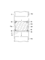
- FIG. 3 is a cross-sectional view taken along line AA in FIG. 2. It is sectional drawing of the optical member sheet
- This embodiment demonstrates the film bonding system which comprises the one part as a production system of an optical display device.
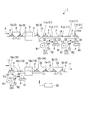
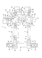
- FIG. 1 is a schematic configuration diagram of a film bonding system 1 of the present embodiment.
- the film laminating system 1 is for laminating a film-shaped optical member such as a polarizing film, a retardation film, or a brightness enhancement film on a panel-shaped optical display component such as a liquid crystal panel or an organic EL panel. And an optical display device including an optical member.
- the liquid crystal panel P is used as the optical display component.
- the film bonding system 1 is illustrated in two upper and lower stages.
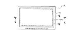
- FIG. 2 is a plan view of the liquid crystal panel P viewed from the thickness direction of the liquid crystal layer P3.
- the liquid crystal panel P includes a first substrate P1 that has a rectangular shape in plan view, a second substrate P2 that has a relatively small rectangular shape disposed to face the first substrate P1, a first substrate P1, and a second substrate. And a liquid crystal layer P3 sealed between the substrate P2.
- the liquid crystal panel P has a rectangular shape that conforms to the outer shape of the first substrate P1 in plan view, and a region that fits inside the outer periphery of the liquid crystal layer P3 in plan view is defined as a display region P4.
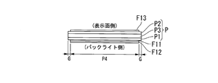
- FIG. 3 is a cross-sectional view taken along the line AA in FIG.
- the front and back surfaces of the liquid crystal panel P are cut out from the first, second, and third optical member sheets F1, F2, and F3 (refer to FIG. 1; hereinafter, sometimes collectively referred to as the optical member sheet FX) having a long strip shape.
- the first, second, and third optical members F11, F12, and F13 (hereinafter may be collectively referred to as the optical member F1X) are appropriately bonded.
- the first optical member F11 and the third optical member F13 as polarizing films are bonded to both the backlight side and the display surface side of the liquid crystal panel P, respectively.
- a second optical member F12 as a brightness enhancement film is further bonded to the first optical member F11.
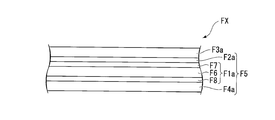
- FIG. 4 is a partial cross-sectional view of the optical member sheet FX bonded to the liquid crystal panel P.
- the optical member sheet FX includes a film-shaped optical member main body F1a, an adhesive layer F2a provided on one surface (the upper surface in FIG. 4) of the optical member main body F1a, and one of the optical member main bodies F1a via the adhesive layer F2a.
- the separator sheet F3a is detachably stacked on the surface, and the surface protection film F4a is stacked on the other surface (the lower surface in FIG. 4) of the optical member body F1a.
- the optical member main body F1a functions as a polarizing plate, and is bonded over the entire display area P4 of the liquid crystal panel P and its peripheral area. For convenience of illustration, hatching of each layer in FIG. 4 is omitted.
- the optical member body F1a is bonded to the liquid crystal panel P via the adhesive layer F2a in a state where the separator sheet F3a is separated while leaving the adhesive layer F2a on one surface thereof.
- seat FX is called the bonding sheet
- the separator sheet F3a protects the adhesive layer F2a and the optical member body F1a before being separated from the adhesive layer F2a.
- the surface protective film F4a is bonded to the liquid crystal panel P together with the optical member body F1a.
- the surface protective film F4a is disposed on the side opposite to the liquid crystal panel P with respect to the optical member body F1a to protect the optical member body F1a.
- the surface protective film F4a is separated from the optical member main body F1a at a predetermined timing.
- the optical member sheet FX may be configured not to include the surface protective film F4a, or the surface protective film F4a may not be separated from the optical member main body F1a.
- the optical member body F1a is bonded to the sheet-like polarizer F6, the first film F7 bonded to one surface of the polarizer F6 with an adhesive or the like, and the other surface of the polarizer F6 with an adhesive or the like. And a second film F8.
- the first film F7 and the second film F8 are protective films that protect the polarizer F6, for example.
- the optical member body F1a may have a single-layer structure composed of a single optical layer, or may have a stacked structure in which a plurality of optical layers are stacked on each other.
- the optical layer may be a retardation film, a brightness enhancement film, or the like.
- At least one of the first film F7 and the second film F8 may be subjected to a surface treatment that provides an effect such as anti-glare including hard coat treatment and anti-glare treatment for protecting the outermost surface of the liquid crystal display element.
- the optical member body F1a may not include at least one of the first film F7 and the second film F8.
- the separator sheet F3a may be bonded to one surface of the optical member body F1a via the adhesive layer F2a.
- FIG. 5 is a plan view (top view) of the film bonding system 1, and the film bonding system 1 will be described below with reference to FIGS.
- an arrow F indicates the transport direction of the liquid crystal panel P.
- the upstream side of the liquid crystal panel P in the transport direction is referred to as the panel transport upstream side
- the downstream side of the liquid crystal panel P in the transport direction is referred to as the panel transport downstream side.
- the film bonding system 1 sets the predetermined position of the main conveyor 5 as the start point 5a and the end point 5b of the bonding process.
- the film laminating system 1 conveys the liquid crystal panel P from the starting point 5a to the first and second sub-conveyors 6 and 7 extending in the direction perpendicular to the main conveyor 5 and from the starting point 5a to the first starting position 6a of the first sub-conveyor 6.
- a second transport device 12 that transports the liquid crystal panel P from the end position 6 b to the first rotary first position 11 a of the first rotary index 11, and a first bonding device 13 and a second paste that are provided around the first rotary index 11. And a film peeling device 14.
- the film bonding system 1 includes a second rotary index 16 provided on the panel transport downstream side of the first rotary index 11 and a second rotary index 16 from the first rotary terminal position 11 b of the first rotary index 11.
- a third transport device 17 that transports the liquid crystal panel P to the rotary starting position 16a, a third bonding device 18 and an inspection device 19 provided around the second rotary index 16, and a panel transport downstream side of the second rotary index 16
- a second conveyor 7 provided on the second rotary conveyor 16
- a fourth conveyor device 21 for conveying the liquid crystal panel P from the second rotary end position 16b of the second rotary index 16 to the second starting position 7a of the second sub conveyor 7, From the second terminal position 7b of the sub-conveyor 7 to the end point 5b of the main conveyor 5, the liquid crystal panel P
- a fifth transport device 22 for transporting.
- the film laminating system 1 performs a predetermined process sequentially on the liquid crystal panel P while transporting the liquid crystal panel P using the lines formed by the drive-type main conveyor 5, the sub-conveyors 6 and 7, and the rotary indexes 11 and 16. Apply.
- the liquid crystal panel P is conveyed on the line with its front and back surfaces being horizontal.
- the liquid crystal panel P is conveyed, for example, in the main conveyor 5 with the short side of the display area P4 along the conveying direction, and in each of the sub conveyors 6 and 7 orthogonal to the main conveyor 5, the long side of the display area P4 is conveyed in the conveying direction.
- each rotary index 11, 16 the long side of the display area P 4 is conveyed in a direction along the radial direction of each rotary index 11, 16.
- Reference numeral 5c in the figure indicates a rack that flows on the main conveyor 5 in correspondence with the liquid crystal panel P.
- the sheet piece (corresponding to the optical member F1X) of the bonding sheet F5 cut out to a predetermined length from the band-shaped optical member sheet FX is bonded to the front and back surfaces of the liquid crystal panel P.
- a control device 25 as an electronic control device.
- the first transport device 8 holds the liquid crystal panel P and transports it freely in the vertical and horizontal directions.
- the first transport device 8 transports, for example, the liquid crystal panel P held by suction to the first starting position 6a (the left end in FIG. 5) of the first sub-conveyor 6 in a horizontal state, and cancels the suction at the position. Then, the liquid crystal panel P is delivered to the first sub-conveyor 6.
- the cleaning device 9 is, for example, a water-washing type that performs brushing and rinsing of the front and back surfaces of the liquid crystal panel P and then drains the front and back surfaces of the liquid crystal panel P.
- the cleaning device 9 may be a dry type that performs static electricity removal and dust collection on the front and back surfaces of the liquid crystal panel P.
- the second transport device 12 holds the liquid crystal panel P and transports it freely in the vertical and horizontal directions. For example, the second transport device 12 transports the liquid crystal panel P held by suction to the first rotary starting position 11a of the first rotary index 11 in a horizontal state, releases the suction at the position, and moves the liquid crystal panel P to the first position. Transfer to one rotary index 11.
- the first rotary index 11 is a disc-shaped rotary table having a rotation axis along the vertical direction, and is driven to rotate clockwise with the left end portion in plan view of FIG. 5 as the first rotary starting position 11a.
- the 1st rotary index 11 makes the position (upper end part of FIG. 5) rotated 90 degrees clockwise from the 1st rotary first departure position 11a the 1st bonding carrying in / out position 11c.
- the liquid crystal panel P is carried into the first bonding apparatus 13 by a transport robot (not shown).
- the liquid crystal panel P is bonded to the first optical member F11 on the backlight side by the first bonding device 13.
- the liquid crystal panel P to which the first optical member F11 is bonded is carried into the first bonding carry-in / out position 11c of the first rotary index 11 from the first bonding device 13 by a transport robot (not shown).
- the 1st rotary index 11 makes the film peeling position 11e the position rotated 45 degrees clockwise from the 1st bonding carrying in / out position 11c (upper right end part of FIG. 5). At the film peeling position 11e, the film peeling device 14 peels the surface protective film F4a of the first optical member F11.
- the 1st rotary index 11 makes the position (right end position of FIG. 5) rotated 45 degrees clockwise from the film peeling position 11e the 2nd bonding carrying in / out position 11d.
- the liquid crystal panel P is carried into the second bonding device 15 by a transport robot (not shown).
- the second optical member F ⁇ b> 12 on the backlight side is bonded by the second bonding device 15.
- the liquid crystal panel P on which the second optical member F12 is bonded is carried into the second bonding carry-in / out position 11d of the first rotary index 11 from the second bonding device 15 by a transport robot (not shown).
- the 1st rotary index 11 makes the position (lower end part of FIG. 5) rotated 90 degrees clockwise from the 2nd bonding carrying in / out position 11d the 1st rotary terminal position 11b. Carrying out by the 3rd conveying apparatus 17 is made
- the third transport device 17 holds the liquid crystal panel P and transports it freely in the vertical and horizontal directions.
- the third transport device 17 transports, for example, the liquid crystal panel P held by suction to the second rotary starting position 16a of the second rotary index 16, and reverses the front and back of the liquid crystal panel P during this transport, so that the second rotary starting position The suction is released at 16 a and the liquid crystal panel P is transferred to the second rotary index 16.
- the second rotary index 16 is a disc-shaped rotary table having a rotation axis along the vertical direction, and is driven to rotate clockwise with the upper end portion in plan view of FIG. 5 as the second rotary starting position 16a.
- the 2nd rotary index 16 makes the position (right end part of FIG. 5) rotated 90 degrees clockwise from the 2nd rotary first departure position 16a the 3rd bonding carrying in / out position 16c.
- the liquid crystal panel P is carried into the third bonding apparatus 18 by a transport robot (not shown).
- the liquid crystal panel P is bonded to the third optical member F13 on the display surface side by the third bonding device 18.
- the liquid crystal panel P on which the third optical member F13 is bonded is carried into the third bonding carry-in / out position 16c of the second rotary index 16 from the third bonding device 18 by a transport robot (not shown).
- the 2nd rotary index 16 makes the position (lower end part of FIG. 5) rotated 90 degrees clockwise from the 3rd bonding carrying in / out position 16c the bonding inspection position 16d. Inspection at the bonding inspection position 16d by the inspection device 19 of the workpiece (liquid crystal panel P) on which the film is bonded (whether the position of the optical member F1X is appropriate (whether the positional deviation is within the tolerance range) ) Etc.) is made. The work determined that the position of the optical member F1X with respect to the liquid crystal panel P is not appropriate is discharged out of the system by a not-shown discharging means.
- the second rotary index 16 has a position (left end portion in FIG. 5) rotated 90 ° clockwise from the bonding inspection position 16d as a second rotary terminal position 16b. Carrying out by the 4th conveying apparatus 21 is made
- the fourth transport device 21 holds the liquid crystal panel P and transports it freely in the vertical and horizontal directions.
- the fourth transport device 21 transports the liquid crystal panel P held by suction to the second starting position 7a of the second sub-conveyor 7, releases the suction at the second starting position 7a, and moves the liquid crystal panel P to the second sub-conveying position 7a. Delivered to the conveyor 7.
- the fifth transport device 22 holds the liquid crystal panel P and transports it freely in the vertical and horizontal directions.
- the fifth transport device 22 transports the liquid crystal panel P held by suction to the end point 5b of the main conveyor 5, releases the suction at the end point 5b, and delivers the liquid crystal panel P to the main conveyor 5.
- FIG. 6 is a schematic side view of the first bonding apparatus 13.
- the 2nd bonding apparatus 15 and the 3rd bonding apparatus 18 abbreviate
- the 1st bonding apparatus 13 bonds the sheet piece (1st optical member F11) of the bonding sheet
- the 1st bonding apparatus 13 unwinds the 1st optical member sheet
- the sheet conveying device 31 that conveys the sheet along the direction, and the sheet conveying device 31 holds the sheet piece (first optical member F11) of the bonding sheet F5 cut out from the first optical member sheet F1, and this sheet piece is a liquid crystal panel.
- a bonding section 40 that is bonded to the upper surface of P.
- the sheet conveying device 31 conveys the bonding sheet F5 using the separator sheet F3a as a carrier, holds the raw fabric roll R1 around which the belt-shaped first optical member sheet F1 is wound, and the first optical member sheet F1.
- the unwinding portion 31a that is fed out along the longitudinal direction, the cutting device 31b that performs a half cut on the first optical member sheet F1 that is unwound from the raw roll R1, and the first optical member sheet F1 that has been subjected to the half cut at an acute angle.
- the sheet conveying apparatus 31 has a some guide roller which winds the 1st optical member sheet
- the first optical member sheet F1 is equivalent to the width of the display area P4 of the liquid crystal panel P (corresponding to the short side length of the display area P4 in this embodiment) in the horizontal direction (sheet width direction) orthogonal to the conveying direction.
- the unwinding unit 31a positioned at the start point of the sheet conveying device 31 and the winding unit 31d positioned at the end point of the sheet conveying device 31 are driven in synchronization with each other, for example.
- the winding-up part 31d winds up the separator sheet F3a which passed through the knife edge 31c, while the unwinding part 31a delivers the 1st optical member sheet
- the upstream side in the transport direction of the first optical member sheet F1 (separator sheet F3a) in the sheet transport apparatus 31 is referred to as the upstream side of the sheet transport, and the downstream side in the transport direction is referred to as the downstream side of the sheet transport.
- the cutting device 31b has a length equal to the length of the display area P4 (corresponding to the long side length of the display area P4 in this embodiment) in the length direction in which the first optical member sheet F1 is orthogonal to the sheet width direction. Each time it is fed out, a part in the thickness direction of the first optical member sheet F1 is cut across the entire width along the sheet width direction (half cutting is performed).
- the cutting device 31b performs cutting so that the first optical member sheet F1 (separator sheet F3a) is not broken by the tension acting during the conveyance of the first optical member sheet F1 (so that a predetermined thickness remains on the separator sheet F3a).
- the advancing / retreating position of the blade is adjusted, and the half cut is performed to the vicinity of the interface between the adhesive layer F2a and the separator sheet F3a.
- the first optical member sheet F1 after the half cut is cut along the entire width in the sheet width direction of the first optical member sheet F1 by cutting the optical member body F1a and the surface protection film F4a in the thickness direction. Is formed.
- the first optical member sheet F1 is divided into sections having a length corresponding to the long side length of the display region P4 in the longitudinal direction by the cut line. Each section is one sheet piece (first optical member F11) in the bonding sheet F5.
- the knife edge 31c is positioned below the first optical member sheet F1 conveyed substantially horizontally from the left side to the right side in FIG. 6, and extends at least over the entire width in the sheet width direction of the first optical member sheet F1.
- the knife edge 31c is wound so as to be in sliding contact with the separator sheet F3a side of the first optical member sheet F1 after the half cut.
- the knife edge 31c wraps the first optical member sheet F1 at an acute angle at the acute end portion.
- the first optical member sheet F1 peels the separator sheet F3a from the bonding sheet F5 when it is folded at an acute angle at the tip of the knife edge 31c.
- the adhesion layer F2a (bonding surface with the liquid crystal panel P) of the bonding sheet F5 faces downward.
- a separator peeling position 31e Immediately above the tip of the knife edge 31c is a separator peeling position 31e, and an arc-shaped holding surface 32a of a bonding head 32 described later is in contact with the tip of the knife edge 31c from above, so that the sheet piece of the bonding sheet F5
- the surface protective film F4a (surface opposite to the bonding surface) is bonded to the holding surface 32a of the bonding head 32.
- the bonding unit 40 includes a bonding stage 41 that holds the liquid crystal panel P at the time of bonding, a bonding head 32 that has an arc-shaped holding surface 32a that is parallel to the sheet width direction and protrudes downward, and a bonding head.
- the drive device 42 which rotationally drives 32, and the moving device 44 which moves the bonding head 32 via this drive device 42 are provided.
- the driving device 42 and the moving device 44 are electrically connected to the control device 25.
- the control device 25 can independently control the driving of the driving device 42 and the moving device 44.
- the bonding stage 41 is for holding the liquid crystal panel P to which the bonding sheet F5 is bonded.
- the bonding stage 41 holds the liquid crystal panel P by, for example, adsorption.
- the bonding head 32 has an arc-shaped holding surface 32a that is parallel to the sheet width direction and protrudes downward.
- the holding surface 32a has, for example, a weaker bonding force than the bonding surface (adhesive layer F2a) of the bonding sheet F5, and the surface protective film F4a of the bonding sheet F5 can be repeatedly bonded and peeled off.
- the driving device 42 rotates the laminating head 32 so as to tilt along the curvature of the holding surface 32a in parallel with the length direction so as to be centered on the axis along the sheet width direction above the knife edge 31c.
- the drive device 42 can raise and lower the bonding head 32 by a predetermined amount. Tilt of the bonding head 32 by the drive device 42 is performed when the bonding sheet F5 is bonded and held, and when the bonded sheet F5 bonded and held is bonded to the liquid crystal panel P as described later.
- the moving device 44 includes a guide rail 44a provided above between the bonding stage 41 and the sheet conveying device 31, a power unit 44b such as an actuator, and an arm unit 43 movable along the guide rail 44a by the power unit 44b. And having.
- the bonding head 32 is attached to the tip of the arm portion 43 via a drive device 42.
- the guide rail 44a is extended along the paper surface penetration direction (width direction of the bonding sheet
- the moving device 44 moves the bonding head 32 between the sheet conveying device 31 and the bonding stage 41 by moving the arm portion 43 along the guide rail 44a. That is, the moving device 44 is configured such that the bonding head 32 is relatively between the peeling position of the separator sheet F3a of the bonding sheet F5 and the bonding position (bonding stage 41) of the bonding sheet F5 to the liquid crystal panel P. Can be moved to.
- the drive device 42 had the function to raise / lower the bonding head 32
- the moving apparatus 44 (arm part 43) may have the function to raise / lower the bonding head 32.
- the moving device 44 moves the arm part 43 (bonding head 32) to the tip of the knife edge 31c, which is the separation position of the separator sheet F3a.
- the drive device 42 is rotated to a state where the bonding head 32 is inclined so that the holding surface 32a faces downward and the curved one end side (right side in FIG. 6) of the holding surface 32a is on the lower side.
- the driving device 42 lowers the inclined bonding head 32 from above the separator peeling position 31e, thereby pressing the curved one end side of the holding surface 32a against the tip of the knife edge 31c from above, and the separator peeling position 31e.
- seat F5 in is stuck on the holding surface 32a.
- the 1st detection camera 34 which detects the sheet
- the control device 25 performs the cutting of the bonding sheet F5 by the cutting device 31b. That is, the distance along the sheet conveyance path between the detection position by the first detection camera 34 (the optical axis extension position of the first detection camera 34) and the cutting position by the cutting device 31b (the cutting blade advance / retreat position of the cutting device 31b) is This corresponds to the length of the sheet piece of the bonding sheet F5.
- the cutting device 31b is movable along the sheet conveyance path, and this movement changes the distance along the sheet conveyance path between the detection position by the first detection camera 34 and the cutting position by the cutting device 31b.
- the movement of the cutting device 31b is controlled by the control device 25.
- the cutting end is a predetermined reference.
- this deviation is corrected by the movement of the cutting device 31b.
- the first detection camera 34 also detects the defect mark marked on the bonding sheet F5.
- the defect mark is marked by an inkjet or the like from the surface protective film F4a side at the defect point found on the first optical member sheet F1 when the raw roll R1 is manufactured.
- the defects of the optical member sheet FX include, for example, a portion where a foreign substance consisting of at least one of solid, liquid, and gas exists in the optical member sheet FX, and unevenness and scratches on the surface of the optical member sheet FX. Or a portion that becomes a bright spot due to distortion of the optical member sheet FX, material deviation, or the like.
- the control device 25 lowers the bonding head 32 by the driving device 42 and sticks the leading end portion of the bonding sheet F5 to the holding surface 32a, and then cuts the engagement between the driving device 42 and the bonding head 32. To do. Thereby, the bonding head 32 can be tilted freely. In this state, the sheet conveying device 31 performs a feeding operation of the bonding sheet F5.
- the bonding head 32 is tiltable by cutting the engagement with the driving device 42, the bonding head 32 is passively tilted with the feeding of the bonding sheet F5.
- the whole sheet piece of the bonding sheet F5 is bonded to the holding surface 32a by tilting the bonding head 32 while feeding the bonding sheet F5.
- the tilting is locked by engaging with the driving device 42 in this inclined posture, for example.
- the driving device 42 raises the bonding head 32 above the separator peeling position 31e.
- the moving apparatus 44 moves the arm part 43 (bonding head 32) on the bonding stage 41, and bonds the bonding sheet F5 with the bonding head 32 bonded to the liquid crystal panel P as described later. Combine.
- seat F5 by which the fault mark was detected as mentioned above is not bonded to liquid crystal panel P, but the discarding position (discard position) which avoided the bonding stage 41. Move and paste on waste material sheet. Or the process of cutting and sticking the bonding sheet
- the bonding head 32 to which the bonding sheet F5 is bonded moves from the separator peeling position 31e to the bonding stage 41, for example, the bonding sheet F5 bonded and held on the holding surface 32a.
- Both corners of the base end with respect to the tip are imaged by the pair of second detection cameras 35, respectively.
- Detection information of each second detection camera 35 is sent to the control device 25.
- the control device 25 is based on the imaging data of each second detection camera 35, for example, the horizontal direction of the bonding sheet F5 with respect to the bonding head 32 (the moving direction of the bonding head 32 and its orthogonal direction and the rotation direction about the vertical axis). Check the position of.
- control device 25 When the relative position of the bonding head 32 and the bonding sheet F5 is misaligned, the control device 25 performs alignment so that the position of the bonding sheet F5 with respect to the bonding head 32 is set to a predetermined reference position by the driving device 42.
- Control device 25 moves the bonding head 32 to a predetermined position above the bonding stage 41.
- the moving device 44 is arranged so that the positions of the front end portion of the bonding sheet F5 bonded to the holding surface 32a and the end portion of the liquid crystal panel P held on the bonding stage 41 overlap in a plane. Alignment of the bonding head 32 and the bonding stage 41 is performed.
- the control device 25 lowers the bonding head 32 in an inclined state by the drive device 42, so that the front end of the bonding sheet F5 bonded to the holding surface 32a is used as the end of the liquid crystal panel P.
- the state is pressed from above.
- the drive device 42 lowers the bonding head 32 so that the bonding sheet F5 is pressed by the liquid crystal panel P.
- the control device 25 engages the bonding head 32 and the driving device 42 so that the driving force from the driving device 42 can be transmitted to the bonding head 32.
- FIG. 7 is an explanatory diagram of a bonding operation by the first bonding apparatus 13.
- seat F5 currently bonded by the bonding head 32, when it unwinds from the original fabric roll R1, curvature (curl) shall not arise or curvature shall be small enough. .
- the control device 25 drives the drive device 42 and the moving device 44 independently. Specifically, at the time of bonding, the control device 25 performs bonding by moving the bonding head 32 and the liquid crystal panel P relative to each other while pressing the bonding sheet F5 against the liquid crystal panel P as illustrated in FIG.
- the drive device 42 and the moving device 44 are controlled so that torque is sometimes generated along the feeding direction of the bonding sheet F5 from the holding surface 32a to the liquid crystal panel P. Thereby, the bonding head 32 tilts on the liquid crystal panel P in a state where the torque is generated (see FIG. 6).
- the feeding direction of the bonding sheet F5 to the liquid crystal panel P is, for example, from the one end side to the other end side when the bonding sheet F5 is bonded from one end side to the other end side of the liquid crystal panel P.
- the pasting head 32 gives the torque so that the end face of the liquid crystal panel P is brought into contact with the holding member 39 at the time of pasting.
- the holding member 39 may be provided on the bonding stage 41 or may be provided in another device. According to this, since the end surface of liquid crystal panel P is supported by the holding member 39 at the time of bonding, the said torque by the bonding head 32 can be provided favorably.
- the holding member 39 is not necessarily provided. Not needed.
- the bonding operation is performed by cutting the engagement between the bonding head 32 and the driving device 42 and moving the moving device 44 in a state where the bonding head 32 is tiltable.
- control apparatus 25 is based on the conditions (for example, material, thickness, curl state, etc.) of the bonding sheet F5, and the driving conditions (for example, the amount of movement in the bonding head 32) of the driving device 42 and the moving device 44.
- the torque applied to the bonding head 32 can be adjusted by appropriately changing the movement speed, the rotation amount, the rotation speed, or the like.
- the 1st bonding apparatus 13 can store the curvature amount which arises in liquid crystal panel P after bonding of the bonding sheet
- the amount of warpage within a certain range means that the warpage generated in the liquid crystal panel P is within a level that causes no practical problem.
- the 1st bonding apparatus 13 is provided above the bonding stage 41 which is a bonding position, and a pair of 3rd detection cameras 36 for performing horizontal alignment of liquid crystal panel P are provided. (See FIGS. 5 and 6). Also in the 2nd bonding apparatus 15, a pair of 4th detection camera 37 for performing horizontal alignment of liquid crystal panel P is provided above the bonding stage 41 which is a bonding position similarly (FIG. 5). reference).
- Each third detection camera 36 images, for example, both corners on the left side in FIG. 5 of the glass substrate (first substrate P1) of the liquid crystal panel P, and each fourth detection camera 37 includes, for example, a glass substrate of the liquid crystal panel P. Each of the left corners in FIG. 5 is imaged.
- a pair of 5th detection camera 38 for performing horizontal alignment of liquid crystal panel P is provided above the bonding stage 41 which is also a bonding position (FIG. 5). reference).
- Each fifth detection camera 38 images, for example, both corners on the left side in FIG. 5 on the glass substrate of the liquid crystal panel P. Detection information of each of the detection cameras 34 to 38 is sent to the control device 25. It is also possible to use sensors in place of the detection cameras 34 to 38.
- the bonding stage 41 in each bonding apparatus 13, 15, 18 is driven and controlled by the control apparatus 25 based on the detection information of each detection camera 34-38. Thereby, alignment of liquid crystal panel P with respect to the bonding head 32 in each bonding position is performed.
- the bonding sheet F5 from the aligned bonding head 32 By bonding the bonding sheet F5 from the aligned bonding head 32 to the liquid crystal panel P, the bonding variation of the optical member F1X is suppressed, and the optical axis direction of the optical member F1X with respect to the liquid crystal panel P is reduced. The accuracy is improved and the clarity and contrast of the optical display device are increased.
- the film bonding system 1 in the above embodiment is formed by bonding the optical member F1X to the liquid crystal panel P, and the liquid crystal panel P is conveyed with respect to the plurality of liquid crystal panels P conveyed on the line. While the belt-shaped optical member sheet FX having a width corresponding to the display area P4 of the panel P is unwound from the original roll R1, the optical member sheet FX is cut to a length corresponding to the display area P4, and the optical member F1X is cut. Then, the optical device F1X is provided with bonding devices 13, 15, and 18 for bonding the liquid crystal panel P to the liquid crystal panel P, and the bonding devices 13, 15, and 18 remove the optical member sheet FX from the original fabric roll R1.
- Unwinding part 31a which unwinds with separator sheet F3a, and cuts optical member sheet FX leaving separator sheet F3a, and the optical member 1X cutting device 31b, knife edge 31c for separating optical member F1X from separator sheet F3a, and optical member F1X attached to arc-shaped holding surface 32a and held on holding surface 32a
- the bonding head 32 tilting along the curvature of the holding surface 32a and the bonding head 32 are combined with the separator sheet F3a of the optical member F1X.
- the moving device 44 moves between the peeling position (separator peeling position 31e) from the substrate and the bonding position (bonding stage 41) of the optical member F1X to the liquid crystal panel P.
- the bonding head 32 that presses the optical member F1X against the liquid crystal panel P is tilted along the curvature of the holding surface 32a.
- the controller 25 moves the bonding head 32 and the liquid crystal panel P relative to each other while pressing the bonding sheet F5 against the liquid crystal panel P at the time of bonding, so that the holding surface 32a is changed to the liquid crystal panel P at the time of bonding.
- the driving device 42 and the moving device 44 are controlled so as to generate torque along the feeding direction of the pasting sheet F5.
- the band-shaped optical member sheet FX having a width corresponding to the display region P4 is cut to a predetermined length to form the optical member F1X, and the optical member F1X is held in an arc shape by tilting the bonding head 32.
- the optical member F1X is bonded to the liquid crystal panel P by the tilting of the bonding head 32, so that the dimensional variation and bonding variation of the optical member F1X are suppressed, and the frame portion G around the display region P4 is held.
- the optical member F1X is bonded to the liquid crystal panel P by the tilting of the bonding head 32 to which the torque along the feeding direction of the bonding sheet F5 is applied, the liquid crystal panel P after the optical member F1X is bonded to the liquid crystal panel P The warp that occurs can be suppressed. Moreover, the continuous bonding of the optical member F1X becomes easy, and the production efficiency of the optical display device can be increased. Further, the optical member F1X can be smoothly held by the tilt of the arc-shaped holding surface 32a, and the optical member F1X can be reliably bonded to the liquid crystal panel P by the tilt of the arc-shaped holding surface 32a.
- the said film bonding system 1 makes the said knife edge 31c peel the said optical member F1X from the said separator sheet F3a with the bonding surface with the said liquid crystal panel P facing down, and the said bonding head 32 is the said.
- An optical member by moving between the peeling position and the bonding position in a state where the upper surface opposite to the bonding surface is bonded to and held on the holding surface 32a and the bonding surface faces downward.
- the sheet FX is conveyed with the bonding surface on the adhesive layer F2a side facing downward, and it is possible to suppress the occurrence of bonding failure by suppressing scratches on the bonding surface of the optical member sheet FX, adhesion of foreign matters, and the like.
- the said film bonding system 1 carries in the said liquid crystal panel P in a carrying-in position (each rotary starting position 11a, 16a), the said bonding position (each bonding stage 41), and a carrying-out position (each rotary terminal position 11b, 16b).
- a carrying-in position each rotary starting position 11a, 16a
- the said bonding position each bonding stage 41
- a carrying-out position each rotary terminal position 11b, 16b.
- the bonding apparatuses 13, 15, and 18 have a detection means (first detection camera 34) for detecting a defect mark marked on the optical member sheet FX, and the optical member sheet FX.
- the part where the defect mark is detected is held by the bonding head 32 and conveyed to the disposal position (discard position). Therefore, the yield of an optical display device improves and the film bonding system 1 with good productivity can be provided.
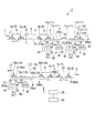
- FIG. 8 is a schematic configuration diagram of the film bonding system 2 of the present embodiment.
- the film bonding system 2 is described in two upper and lower stages.
- the same reference numerals are given to components common to the first embodiment, and detailed description thereof is omitted.
- the width and length of the optical member F1X bonded by the bonding head 32 is equivalent to that in the display region P4 of the liquid crystal panel P is taken as an example.
- a cutting device for cutting off an excess portion of the sheet piece is provided. In this respect, it differs greatly from the first embodiment.
- the film bonding system 2 has long, strip-like first, second, and third optical member sheets F1, F2, and F3 (optical members) on the front and back surfaces of the liquid crystal panel P.
- the first, second and third optical members F11, F12, F13 (optical member F1X) cut out from the sheet FX) are bonded together.
- the first, second, and third optical members F11, F12, and F13 are first, second, and third sheet pieces F1m, F2m, and F3m (hereinafter collectively referred to as sheet pieces FXm). In other cases, the excess portion outside the display area is cut off.
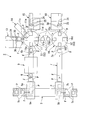
- FIG. 9 is a plan view (top view) of the film bonding system 2, and the film bonding system 2 will be described below with reference to FIGS.
- an arrow F indicates the transport direction of the liquid crystal panel P.
- the upstream side in the transport direction of the liquid crystal panel P is referred to as the upstream side of the panel transport
- the downstream side in the transport direction of the liquid crystal panel P is referred to as the downstream side of the panel transport.
- the film bonding system 2 sets the predetermined position of the main conveyor 5 as the start point 5a and the end point 5b of the bonding process.
- the film bonding system 2 includes a first sub conveyor 6 and a second sub conveyor 7, a first conveying device 8, a cleaning device 9, a first rotary index 11, a second conveying device 12, and a first bonding.
- the apparatus 13 and the 2nd bonding apparatus 15, the film peeling apparatus 14, and the 1st cutting device 51 are provided.
- the film bonding system 2 includes a second rotary index 16 provided on the panel transport downstream side of the first rotary index 11, a third transport device 17, a third bonding device 18, and a second cutting device 52.
- the second sub-conveyor 7, the fourth transport device 21, and the fifth transport device 22 are provided.
- the film laminating system 2 uses the lines formed by the driven main conveyor 5, the sub conveyors 6 and 7, and the rotary indexes 11 and 16 to transfer the liquid crystal panel P to the liquid crystal panel P in order. Apply.
- the liquid crystal panel P is conveyed, for example, in the main conveyor 5 with the short side of the display area P4 along the conveying direction, and in each of the sub conveyors 6 and 7 orthogonal to the main conveyor 5, the long side of the display area P4 is conveyed in the conveying direction.
- the long side of the display area P 4 is conveyed in a direction along the radial direction of each rotary index 11, 16.
- the film bonding system 2 bonds a sheet piece (corresponding to the optical member F1X) of the bonding sheet F5 cut out to a predetermined length from the belt-shaped optical member sheet FX on the front and back surfaces of the liquid crystal panel P.
- the first rotary index 11 is driven to rotate clockwise with the carry-in position from the second transport device 12 (left end portion in plan view in FIG. 9) as the first rotary starting position 11a.
- the 1st rotary index 11 makes the position (upper end part of FIG. 9) rotated 90 degrees clockwise from the 1st rotary starting position 11a the 1st bonding carrying in / out position 11c.
- the liquid crystal panel P is carried into the first bonding apparatus 13 by a transport robot (not shown).
- seat piece F1m of the backlight side in liquid crystal panel P is bonded by the 1st bonding apparatus 13.
- FIG. The first sheet piece F1m is a sheet piece of the first optical member sheet F1 having a size larger than the display area P4 of the liquid crystal panel P.
- the 1st optical member bonding body PA1 is formed when the 1st sheet piece F1m is bonded by the 1st bonding apparatus 13 on the surface one side of liquid crystal panel P. As shown in FIG. 1st optical member bonding body PA1 is carried in from the 1st bonding apparatus 13 to the 1st bonding carrying in / out position 11c of the 1st rotary index 11 by the conveyance robot not shown.
- the 1st rotary index 11 makes the film peeling position 11e the position rotated 45 degrees clockwise from the 1st bonding carry-in / out position 11c (upper right end part of FIG. 9). At the film peeling position 11e, the film peeling device 14 peels the surface protection film F4a of the first sheet piece F1m.
- the 1st rotary index 11 makes the position (right end position of FIG. 9) rotated 45 degrees clockwise from the film peeling position 11e the 2nd bonding carrying in / out position 11d.
- the liquid crystal panel P is carried into the second bonding apparatus 15 by a transport robot (not shown).
- the 2nd bonding apparatus 15 bonds the 2nd sheet piece F2m by the side of the backlight in liquid crystal panel P.
- the second sheet piece F2m is a sheet piece of the second optical member sheet F2 having a size larger than the display area of the liquid crystal panel P.
- the 2nd optical member bonding body PA2 is formed by the 2nd bonding apparatus 15 bonding the 2nd sheet piece F2m to the surface at the side of the 1st sheet piece F1m of 1st optical member bonding body PA1.
- 2nd optical member bonding body PA2 is carried in from the 2nd bonding apparatus 15 to the 2nd bonding carrying in / out position 11d of the 1st rotary index 11 by the conveyance robot not shown.
- the 1st rotary index 11 makes the position (lower end part of FIG. 9) rotated 90 degrees clockwise from the 2nd bonding position 11d the 1st rotary terminal position (1st cutting position) 11b.
- the first rotary terminal position 11b is a first cutting position where the first sheet piece F1m and the second sheet piece F2m are cut by the first cutting device 51.
- the 1st cutting device 51 puts together the excess part arrange
- the first optical member F11 made of the first optical member sheet F1 and the second optical member F12 made of the second optical member sheet F2 are formed as optical members having a size corresponding to the display area P4 of the liquid crystal panel P. .
- the “part facing the display region P4” is a region having a size not less than the size of the display region P4 and not more than the size of the outer shape of the optical display component (liquid crystal panel P). And the area
- the first optical member F11 and the second optical member F12 are not misaligned, and the outside of the display area P4.
- the first optical member F11 and the second optical member F12 that match the shape of the periphery are obtained.
- the cutting process of the 1st sheet piece F1m and the 2nd sheet piece F2m is also simplified.
- the first optical device F11 and the first optical member F11 and the second surface piece of the liquid crystal panel P are separated from the first and second surfaces of the liquid crystal panel P by separating the excess portions of the first sheet piece F1m and the second sheet piece F2m from the second optical member bonding body PA2 by the first cutting device 51.
- 3rd optical member bonding body PA3 formed by bonding 2 optical member F12 is formed.
- the surplus part cut off from the first sheet piece FX1 and the second sheet piece F2m is peeled off and collected from the liquid crystal panel P by a peeling device (not shown).
- 3rd optical member bonding body PA3 is carried out by the 3rd conveying apparatus 17 in the 1st rotary terminal position 11b.
- 3rd conveyance apparatus 17 hold maintains liquid crystal panel P (3rd optical member bonding body PA3), and conveys it freely in a vertical direction and a horizontal direction.
- the third transport device 17 transports, for example, the liquid crystal panel P held by suction to the second rotary starting position 16a of the second rotary index 16, and reverses the front and back of the liquid crystal panel P during this transport, so that the second rotary starting position The suction is released at 16 a and the liquid crystal panel P is transferred to the second rotary index 16.
- the second rotary index 16 is driven to rotate clockwise with the carry-in position from the third transport device 17 (the upper end portion in plan view in FIG. 9) as the second rotary initial position 16a.
- the 2nd rotary index 16 makes the position (right end part of FIG. 9) rotated 90 degrees clockwise from the 2nd rotary initial position 16a the 3rd bonding carrying in / out position 16c.
- the liquid crystal panel P is carried into the third bonding apparatus 18 by a transport robot (not shown).
- the 3rd bonding apparatus 18 bonds the 3rd sheet piece F3m by the side of a display surface.
- the third sheet piece F3m is a sheet piece of the third optical member sheet F3 having a size larger than the display area of the liquid crystal panel P.
- the third bonding device 18 changes the surface of the liquid crystal panel P to the other surface (the surface opposite to the surface on which the first optical member F11 and the second optical member F12 of the third optical member bonding body PA3 are bonded).
- the fourth optical member bonding body PA4 is formed by bonding the three sheet pieces F3m. 4th optical member bonding body PA4 is carried in from the 3rd bonding apparatus 18 to the 3rd bonding carrying in / out position 16c of the 2nd rotary index 16 by the conveyance robot not shown.
- the 2nd rotary index 16 makes the position (lower end part of FIG. 9) rotated 90 degrees clockwise from the 3rd bonding position 16c the 2nd cutting position 16d.
- the third sheet piece F3m is cut by the second cutting device 52.
- the third optical member F13 is bonded to the other side of the front and back surfaces of the liquid crystal panel P by separating the excess portion of the third sheet piece F3m from the fourth optical member bonding body PA4 by the second cutting device 52, and the liquid crystal
- the 5th optical member bonding body PA5 formed by bonding the 1st optical member F11 and the 2nd optical member F12 to the surface one side of the panel P is formed.
- the surplus part cut off from the third sheet piece F3m is peeled off and collected from the liquid crystal panel P by a peeling device (not shown).
- the first cutting device 51 and the second cutting device 52 are, for example, CO2 laser cutters.
- the structure of the 1st and 2nd cutting devices 51 and 52 is not limited to this, For example, it is also possible to use other cutting means, such as a cutting blade.
- the first cutting device 51 and the second cutting device 52 cut the sheet piece FXm bonded to the liquid crystal panel P in an endless manner along the outer peripheral edge of the display region P4.
- the first cutting device 51 and the second cutting device 52 are connected to the same laser output device 53.
- the excess portion disposed outside the portion facing the display region P4 is separated from the sheet piece FXm, and an optical having a size corresponding to the display region P4.
- Cutting means for forming the member sheet FX is configured.
- the high-power laser light output from the laser output device 53 is branched into two, and the first cutting device 51 and the second cutting device. You may supply to the apparatus 52.
- FIG. 1 the high-power laser light output from the laser output device 53 is branched into two, and the first cutting device 51 and the second cutting device. You may supply to the apparatus 52.
- the second rotary index 16 has a position (left end portion in FIG. 9) rotated 90 ° clockwise from the second cutting position 16d as the second rotary terminal position 16b.
- the fifth optical member bonding body PA5 is carried out by the fourth transport device 21 at the second rotary terminal position 16b.
- the 4th conveyance apparatus 21 hold maintains liquid crystal panel P (5th optical member bonding body PA5), and conveys it freely in a perpendicular direction and a horizontal direction.
- the fourth transport device 21 transports the liquid crystal panel P held by suction to the second starting position 7a of the second sub-conveyor 7, releases the suction at the second starting position 7a, and moves the liquid crystal panel P to the second sub-conveying position 7a. Delivered to the conveyor 7.
- the fifth transport device 22 holds the liquid crystal panel P (fifth optical member bonding body PA5) and transports it freely in the vertical and horizontal directions.
- the fifth transport device 22 transports the liquid crystal panel P held by suction to the end point 5b of the main conveyor 5, releases the suction at the end point 5b, and delivers the liquid crystal panel P to the main conveyor 5.
- An unillustrated bonding inspection position is installed on the transport path of the liquid crystal panel P (fifth optical member bonding body PA5) after the second rotary terminal position 16b, and film bonding is performed at this bonding inspection position.
- An inspection (not shown) of the workpiece (liquid crystal panel P) subjected to the inspection is performed.
- the work determined that the position of the optical member F1X with respect to the liquid crystal panel P is not appropriate is discharged out of the system by a not-shown discharging means.
- the first bonding apparatus 13 will be described with an example of the bonding process of the bonding sheet F5 to the liquid crystal panel P.
- description about the bonding process by the 2nd and 3rd bonding apparatuses 15 and 18 which have the same structure as the 1st bonding apparatus 13 is abbreviate
- the 1st bonding apparatus 13 cuts out the sheet piece (1st sheet piece F1m) of the bonding sheet
- the 1st bonding apparatus 13 bonds the sheet piece (1st sheet piece F1m) of the bonding sheet
- the bonding stage 41 is driven and controlled by the control device 25 based on the detection information of the detection cameras 34 to 38. Thereby, alignment of liquid crystal panel P with respect to the bonding head 32 in each bonding position is performed.
- the bonding sheet F5 sheet piece FXm
- the bonding variation of the optical member F1X is suppressed, and the optical member F1X for the liquid crystal panel P is suppressed.
- the accuracy in the optical axis direction of the optical display device is improved, and the vividness and contrast of the optical display device are increased.
- the polarizer film constituting the optical member sheet FX is formed by, for example, uniaxially stretching a PVA film dyed with a dichroic dye, but the PVA film has uneven thickness or dichroism when stretched. There may be a variation in the direction of the academic axis in the plane of the optical member sheet FX due to uneven coloring of the pigment.
- the control device 25 uses the liquid crystal panel for the optical member sheet FX based on the inspection data of the in-plane distribution of the optical axis in each part of the optical member sheet FX stored in advance in the storage device 24 (see FIG. 8).
- P bonding position (relative bonding position) is determined.
- each bonding apparatus 13,15,18 aligns liquid crystal panel P with respect to the sheet piece FXm cut out from the optical member sheet
- the determination method of the bonding position (relative bonding position) of the sheet piece FXm to the liquid crystal panel P is, for example, as follows.
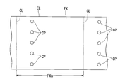
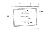
- a plurality of inspection points CP are set in the width direction of the optical member sheet FX, and the direction of the optical axis of the optical member sheet FX is detected at each inspection point CP.
- the timing for detecting the optical axis may be at the time of manufacturing the original fabric roll R1, or may be until the optical member sheet FX is unwound from the original fabric roll R1 and half cut.
- Data in the optical axis direction of the optical member sheet FX is stored in a storage device (not shown) in association with the position of the optical member sheet FX (position in the longitudinal direction and position in the width direction of the optical member sheet FX).
- the control device 25 acquires the optical axis data (inspection data of the in-plane distribution of the optical axis) of each inspection point CP from the storage device (not shown), and the optical member sheet FX (cut) of the portion from which the sheet piece FXm is cut out. The direction of the average optical axis in the area defined by the lead-in line CL is detected.
- an angle (deviation angle) formed between the direction of the optical axis and the edge line EL of the optical member sheet FX is detected for each inspection point CP, and the largest of the deviation angles (maximum deviation).
- the direction that forms the average deviation angle ⁇ mid with respect to the edge line EL of the optical member sheet FX is detected as the average direction of the optical axis of the optical member sheet FX.
- the deviation angle is calculated, for example, with the counterclockwise direction being positive with respect to the edge line EL of the optical member sheet FX and the clockwise direction being negative.
- the direction of the average optical axis of the optical member sheet FX detected by the above method makes a desired angle with respect to the long side or the short side of the display region P4 of the liquid crystal panel P.
- the bonding position (relative bonding position) of the sheet piece FXm is determined. For example, when the direction of the optical axis of the optical member F1X is set to be 90 ° with respect to the long side or the short side of the display region P4 according to the design specifications, the average optical axis of the optical member sheet FX is set.
- the sheet piece FXm is bonded to the liquid crystal panel P so that the direction is 90 ° with respect to the long side or the short side of the display region P4.
- torque is applied to the bonding head 32 by independently controlling the moving device 44 and the driving device 42.
- the tensile stress and balance to the head side received from the 1st sheet piece F1m stuck to the bonding head 32 are adjusted. Therefore, also in this embodiment, the curvature amount which arises in liquid crystal panel P after bonding of the 1st sheet piece F1m can be stored in a fixed range.
- the above-described cutting devices 51 and 52 detect the outer peripheral edge of the display area P4 of the liquid crystal panel P with a detecting means such as a camera, and the sheet piece FXm bonded to the liquid crystal panel P is along the outer peripheral edge of the display area P4. Cut endlessly.
- the outer peripheral edge of the display area P4 is detected by imaging the edge of the liquid crystal panel P, the alignment mark provided on the liquid crystal panel P, or the outermost edge of the black matrix provided in the display area P4.
- a frame portion G (see FIG. 3) having a predetermined width for arranging a sealant or the like for bonding the first and second substrates of the liquid crystal panel P is provided.
- the sheet piece FXm is cut by the cutting devices 51 and 52.
- seat FX is not limited to the said method.
- one or a plurality of inspection points CP is selected from a plurality of inspection points CP (see FIG. 10A) set in the width direction of the optical member sheet FX, and the direction of the optical axis is selected for each selected inspection point CP.
- the angle (deviation angle) formed by the edge line EL of the optical member sheet FX is detected.
- the average value of the deviation angles in the optical axis direction of the selected one or more inspection points CP is detected as the average deviation angle, and the direction forming the average deviation angle with respect to the edge line EL of the optical member sheet FX is optically detected. You may detect as the direction of the average optical axis of member sheet FX.
- the film bonding system 2 of the present embodiment is a strip-shaped optical member sheet FX having a width wider than the length of either one of the long side and the short side of the display region P4 of the liquid crystal panel P. Is unwound from the raw roll R1, and the optical member sheet FX is cut to a length longer than the length of either one of the long side and the short side of the display region P4 to obtain a sheet piece FXm, The sheet apparatus FXm is bonded to the liquid crystal panel P to form an optical member bonded body, and the outside of the portion facing the display region P4 from the sheet piece FXm bonded to the liquid crystal panel P.
- Cutting devices 51 and 52 that cut off the arranged surplus portion and form an optical member F1X having a size corresponding to the display region P4. Therefore, the optical member F1X can be accurately provided up to the display area P4, and the frame portion G (see FIG. 3) outside the display area P4 can be narrowed to enlarge the display area and downsize the device. Moreover, since the bonding head 32 gives a torque to the sheet piece FXm at the time of bonding of the sheet piece FXm, the amount of warpage generated in the liquid crystal panel P after bonding of the optical member F1X is suppressed as in the first embodiment. Can do.
- the 1st cutting device 51 and the 2nd cutting device 52 are laser cutters, the 1st cutting device 51 and the 2nd cutting device 52 are connected to the same laser output device 53,
- the laser output from the laser output device 53 may be branched and supplied to the first cutting device 51 and the second cutting device 52.
- the production system of the optical display device can be downsized.
- the present invention is not limited to the above-described embodiment, and various modifications can be made without departing from the spirit of the present invention, including the component configuration, structure, shape, size, number, arrangement, and the like.
- the case where the movement apparatus 44 moved the bonding head 32 at the time of bonding performed the relative movement of liquid crystal panel P and the bonding head 32 was mentioned as an example, but the bonding head 32 was mentioned.
- a configuration may be adopted in which the liquid crystal panel P is moved relative to the bonding head 32 by moving the bonding stage 41 without moving.
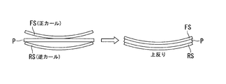
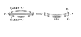
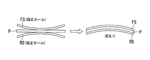
- FIGS. 11A to 11C there are three patterns as shown in FIGS. 11A to 11C.
- the bonding sheet bonded by the display surface side of liquid crystal panel P is called front side sheet
- FIG. 11A shows that the front side sheet FS has a relatively strong warp convex on the liquid crystal panel P side (hereinafter sometimes referred to as a strong curl), and the rear side sheet RS protrudes on the opposite side of the liquid crystal panel P.
- the case of having a relatively weak warpage (hereinafter also referred to as weak reverse curl) is shown.
- FIG. 11B shows a case where the front seat FS has a normal curl and the rear seat RS has a reverse curl of the same strength.
- FIG. 11C shows a case where the front side seat FS has a weak weak reverse curl and the rear side seat RS has a relatively strong strong reverse curl.
- the bonding head 32 When pasting the front sheet FS and the rear sheet RS in a combination that causes warping as shown in FIGS. 11A to 11C, the bonding head 32 is bonded to the liquid crystal panel P when the front sheet FS is bonded. The torque is applied so that the torque is not applied to the bonding head 32 when the rear sheet RS is bonded to the liquid crystal panel P. According to this, it has been confirmed that the liquid crystal panel P to which the front side sheet FS and the rear side sheet RS are bonded is prevented from warping.
- the torque is applied when the bonding sheet F5 is bonded to one surface (display surface) of the liquid crystal panel P.
- the bonding sheet F5 is bonded to the other surface (back surface)
- the warpage generated in the liquid crystal panel P after bonding can be suppressed by not applying the torque.
- seat F5 bonded by the display surface side of liquid crystal panel P is called the front side sheet
- seat F5 bonded by the other side is a rear side sheet
- FIG. 12A shows a case where the front side seat FS has a relatively weak positive curl and the rear side seat RS has a relatively strong positive curl.
- FIG. 12B shows a case where the front side seat FS has a reverse curl and the rear side seat RS has a normal curl of the same strength.
- FIG. 12C shows a case where the front side seat FS has a relatively strong strong reverse curl and the rear side seat RS has a relatively weak weak reverse curl.
- the present invention can be applied by appropriately applying the above torque when the bonding sheet F5 is bonded to at least one surface of the liquid crystal panel P based on the curl characteristics generated in advance in the bonding sheet F5.
- the amount of warpage occurring in the liquid crystal panel P after joining can be suppressed.
- the holding member 39 is provided only in the one end side (left end side in FIG. 7) where the bonding sheet
- the holding member 39 may be provided on the other end side (right end side in FIG. 7) or both sides (left and right sides of the liquid crystal panel P in FIG. 7) where the bonding sheet F5 is bonded to the liquid crystal panel P. Good.
- the bonding head 32 may apply the torque so that the end face of the liquid crystal panel P is brought into contact with the holding member 39 provided on the other end side. That is, the bonding head 32 applies torque to the liquid crystal panel P along the direction opposite to the direction in which the torque is shown in FIG. 7 (the direction opposite to the arrow in the left direction shown in FIG. 7). You may make it suppress the curvature amount which arises in liquid crystal panel P after joining. Even when the torque is applied in the reverse direction as described above, as in the case described with reference to FIG. 7, for example, the liquid crystal panel P is strongly adsorbed by the bonding stage 41. When there is no deviation in the suction position on the bonding stage 41, the holding member 39 is not necessarily provided.
- the size of the surplus portion of the sheet piece FXm (the size of the portion that protrudes outside the liquid crystal panel P) is appropriately set according to the size of the liquid crystal panel P.
- the distance between one side of the sheet piece FXm and one side of the liquid crystal panel P is 2 mm on each side of the sheet piece FXm. Set to a length in the range of ⁇ 5 mm.
- the film bonding system according to the third embodiment of the present invention will be described with reference to FIGS. 13 to 15, the illustration of the second sheet piece F2m is omitted for convenience.
- symbol is attached
- the optical member F1X in this embodiment is formed by separating the excess part of the outer side of the bonding surface from the sheet piece FXm bonded to the liquid crystal panel P.
- the film bonding system includes a first detection device 91 (see FIG. 14).
- the 1st detection apparatus 91 is provided in a panel conveyance downstream rather than the 2nd bonding position 11d.
- the 1st detection apparatus 91 detects the edge of the bonding surface (henceforth a 1st bonding surface) of liquid crystal panel P and the 1st sheet piece F1m.
- the first detection device 91 has an edge ED (outside of the bonding surface) of the first bonding surface SA1 in the four inspection areas CA installed on the conveyance path of the upstream conveyor 6. ).
- region CA is arrange
- the edge ED is detected for each liquid crystal panel P conveyed on the line.
- the edge ED data detected by the first detection device 91 is stored in the storage device 24 (see FIG. 8).
- region CA may be arrange
- FIG. 14 is a schematic diagram of the first detection device 91.
- the first detection device 91 has an illumination light source 94 that illuminates the edge ED and the first bonding surface SA1 rather than the edge ED with respect to the normal direction of the first bonding surface SA1.
- An image pickup device 93 that is arranged at a position inclined inward and picks up an image of the edge ED from the side on which the first sheet piece F1m of the first optical member bonding body PA1 is bonded.
- the illumination light source 94 and the imaging device 93 are respectively arranged in the four inspection areas CA (positions corresponding to the four corners of the first bonding surface SA1) shown in FIG.
- An angle ⁇ (hereinafter referred to as an inclination angle ⁇ of the imaging device 93) formed by the normal line of the first bonding surface SA1 and the normal line of the imaging surface 93a of the imaging device 93 is divided into panels within the imaging field of the imaging device 93. It is preferable to set so that time lag, burrs and the like do not enter. For example, when the end surface of the second substrate P2 is shifted outward from the end surface of the first substrate P1, the inclination angle ⁇ of the imaging device 93 is such that the edge of the second substrate P2 enters the imaging field of the imaging device 93. Set to not.
- the inclination angle ⁇ of the imaging device 93 is set so as to match the distance H between the first bonding surface SA1 and the center of the imaging surface 93a of the imaging device 93 (hereinafter referred to as the height H of the imaging device 93). It is preferred that for example, when the height H of the imaging device 93 is 50 mm or more and 100 mm or less, the inclination angle ⁇ of the imaging device 93 is preferably set to an angle in the range of 5 ° or more and 20 ° or less. However, when the deviation amount is empirically known, the height H of the imaging device 93 and the inclination angle ⁇ of the imaging device 93 can be obtained based on the deviation amount. In the present embodiment, the height H of the imaging device 93 is set to 78 mm, and the inclination angle ⁇ of the imaging device 93 is set to 10 °.
- the illumination light source 94 and the imaging device 93 are fixedly arranged in each inspection area CA.
- the illumination light source 94 and the imaging device 93 may be arrange
- the illumination light source 94 is arrange
- the illumination light source 94 is arrange
- the optical axis of the illumination light source 94 and the normal line of the imaging surface 93a of the imaging device 93 are parallel.
- the illumination light source may be arrange
- optical axis of the illumination light source 94 and the normal line of the imaging surface 93a of the imaging device 93 may slightly cross each other.
- each of the imaging device 93 and the illumination light source 94 may be arranged at a position overlapping the edge ED along the normal direction of the first bonding surface SA1.
- a distance H1 between the first bonding surface SA1 and the center of the imaging surface 93a of the imaging device 93 (hereinafter referred to as a height H1 of the imaging device 93) detects the edge ED of the first bonding surface SA1. It is preferable to set the position at an easy position.
- the height H1 of the imaging device 93 is preferably set in a range of 50 mm or more and 150 mm or less.
- the cut position of the first sheet piece F1m is adjusted based on the detection result of the edge ED of the first bonding surface SA1.
- the control device 25 acquires the data of the edge ED of the first bonding surface SA1 stored in the storage device 24 (see FIG. 8), and the first optical member F11 is outside the liquid crystal panel P (see FIG. 8).
- the cut position of the 1st sheet piece F1m is determined so that it may become the magnitude
- the first cutting device 51 cuts the first sheet piece F1m at the cutting position determined by the control device 25.
- the first cutting device 51 is provided on the downstream side of the panel conveyance with respect to the first detection device 91.
- the 1st cutting device 51 puts together the excess part arrange
- the first optical member F11 made of the first optical member sheet F1 and the second optical member F12 made of the second optical member sheet F2 are formed as optical members having a size corresponding to the first bonding surface SA1.
- the “size corresponding to the first bonding surface SA1” is not less than the size of the display region P4 and not more than the size of the outer shape (contour shape in plan view) of the liquid crystal panel P, and Indicates the size of the area that avoids functional parts such as electrical component mounting parts.
- the first cutting device 51 cuts off the excess portions of the first sheet piece F1m and the second sheet piece F2m from the second optical member bonding body PA2, so that the first optical member F11 and the first optical member F11 on the front and back surfaces of the liquid crystal panel P are separated.
- 3rd optical member bonding body PA3 formed by bonding 2 optical member F12 is formed.
- the 3rd optical member bonding body PA3 and the part (each optical member F11, F12) corresponding to 1st bonding surface SA1 are cut off, and the surplus part of each sheet piece F1m, F2m which remains in frame shape.
- the surplus part cut off from the first sheet piece FX1 and the second sheet piece F2m is peeled off and collected from the liquid crystal panel P by a peeling device (not shown).
- the “part corresponding to the first bonding surface SA1” is a region that is not less than the size of the display region P4 and not more than the size of the outer shape of the liquid crystal panel P, and a functional part such as an electrical component mounting portion. Indicates the area that was avoided.
- the surplus portion is laser-cut along the outer peripheral edge of the liquid crystal panel P, and in one side corresponding to the functional portion, the liquid crystal The surplus portion is laser-cut at a position that appropriately enters the display region P4 side from the outer peripheral edge of the panel P.
- a sheet piece is pasted in a region avoiding the functional portion in the liquid crystal panel P in advance, and then along the outer peripheral edge of the liquid crystal panel P on three sides excluding the functional portion in the liquid crystal panel P having a rectangular shape in plan view. The excess portion may be laser cut.
- a film bonding system is provided with the 2nd detection apparatus 92 (refer FIG. 14).
- the 2nd detection apparatus 92 is provided in the panel conveyance downstream rather than the 3rd bonding position 16c.
- the 2nd detection apparatus 92 detects the edge of the bonding surface (henceforth a 2nd bonding surface) of liquid crystal panel P and the 3rd sheet piece F3m.
- the edge data detected by the second detection device 92 is stored in the storage device (see FIG. 8).
- the cut position of the third sheet piece F3m is adjusted based on the detection result of the edge of the second bonding surface.
- the control device 25 acquires the edge data of the second bonding surface stored in the storage device 24 (see FIG. 8), and the third optical member F13 is outside the liquid crystal panel P (second The cut position of the 3rd sheet piece F3m is determined so that it may become the magnitude
- the second cutting device 52 cuts the third sheet piece F3m at the cutting position determined by the control device 25.
- the second cutting device 52 is provided on the downstream side of the panel conveyance with respect to the second detection device 92.
- the 2nd cutting device 52 cut
- the optical member (third optical member F13) is formed.
- the “size corresponding to the second bonding surface” is a size not less than the size of the display region P4 and not more than the size of the outer shape (contour shape in plan view) of the liquid crystal panel P, and electric Indicates the size of the area that avoids the functional parts such as the parts mounting part. In the present embodiment, it is the size of the outer shape of the second substrate P2.
- the third optical member F13 is bonded to the other side of the front and back surfaces of the liquid crystal panel P by separating the excess portion of the third sheet piece F3m from the fourth optical member bonding body PA4 by the second cutting device 52, and the liquid crystal
- the 5th optical member bonding body PA5 formed by bonding the 1st optical member F11 and the 2nd optical member F12 to the surface one side of the panel P is formed.
- the 5th optical member bonding body PA5 and the excess part of the 3rd sheet piece F3m which a part (3rd optical member F13) corresponding to a 2nd bonding surface is cut off, and remain in frame shape are isolate
- the surplus part cut off from the third sheet piece F3m is peeled off and collected from the liquid crystal panel P by a peeling device (not shown).
- the “part corresponding to the second bonding surface” is a region that is not less than the size of the display region P4 and not more than the size of the outer shape of the liquid crystal panel P, and a functional part such as an electrical component mounting portion. Indicates the area that was avoided.
- the surplus portions are laser-cut along the outer peripheral edge of the liquid crystal panel P on the four sides of the liquid crystal panel P having a rectangular shape in plan view. For example, when the portion corresponding to the second bonding surface is the bonding surface of the CF substrate, there is no portion corresponding to the functional portion, so that the four sides of the liquid crystal panel P are cut along the outer peripheral edge of the liquid crystal panel P. .
- the 1st cutting device 51 is a 1st sheet
- Each of the piece F1m and the second sheet piece F2m is cut.
- the film bonding system of the present embodiment after the sheet piece FXm larger than the display region P4 is bonded to the liquid crystal panel P, the liquid crystal panel P and the sheet on which the sheet piece FXm is bonded.
- the bonding surface By detecting the outer peripheral edge of the bonding surface with the piece FXm and cutting off the surplus portion arranged outside the portion corresponding to the bonding surface from the sheet piece FXm bonded to the liquid crystal panel P, the bonding surface The corresponding size optical member F1X can be formed on the surface of the liquid crystal panel P.
- the optical member F1X can be accurately provided up to the display area P4, and the frame area G outside the display area P4 can be narrowed to enlarge the display area and downsize the device.
- the outer periphery of the bonding surface is detected for every some liquid crystal panel P using a detection apparatus, and it pastes for every liquid crystal panel P based on the detected outer periphery.
- Second detection device detection device
- P... Liquid crystal panel optical display component
- P4... Display region F1.
- Member sheet F3 ... third optical member sheet (optical) Material sheet)
- FX ... optical member sheet, F3a ... separator sheet
Landscapes
- Physics & Mathematics (AREA)
- Nonlinear Science (AREA)
- General Physics & Mathematics (AREA)
- Crystallography & Structural Chemistry (AREA)
- Chemical & Material Sciences (AREA)
- Optics & Photonics (AREA)
- Manufacturing & Machinery (AREA)
- Engineering & Computer Science (AREA)
- Devices For Indicating Variable Information By Combining Individual Elements (AREA)
- Liquid Crystal (AREA)
- Mathematical Physics (AREA)
- Laminated Bodies (AREA)
- Polarising Elements (AREA)
- Folding Of Thin Sheet-Like Materials, Special Discharging Devices, And Others (AREA)
Abstract
L'invention concerne un système permettant de produire des dispositifs d'affichage optique comprenant un dispositif de laminage qui, pour une pluralité de composants d'affichage optique (P) transportés sur une ligne, déroule une feuille d'élément optique en forme de ceinture (F1) ayant une largeur correspondant à la zone d'affichage des composants d'affichage optique à partir d'un rouleau de feuille entière (R1), et ce faisant, découpe la feuille d'élément optique à une longueur correspondant à la zone d'affichage afin d'obtenir un élément optique (F11), puis lamine l'élément optique sur le composant d'affichage optique. Le dispositif de laminage comprend : une tête de laminage (32) dans laquelle l'élément optique maintenu en place en étant collé à une surface de maintien en forme d'arc (32a) est laminé sur le composant d'affichage optique ; un dispositif de déplacement (44) permettant de déplacer la tête de laminage et le composant d'affichage optique l'un par rapport à l'autre pendant le laminage de l'élément optique ; et un dispositif de commande (42) permettant de commander la tête de laminage de telle sorte que la tête de laminage soit inclinée le long de la courbe de la surface de maintien pendant le laminage de l'élément optique, la tête de laminage pressant l'élément optique contre le composant d'affichage optique.
Priority Applications (2)
| Application Number | Priority Date | Filing Date | Title |
|---|---|---|---|
| CN201480007237.0A CN104969281B (zh) | 2013-03-21 | 2014-03-19 | 光学显示设备的生产系统以及生产方法 |
| KR1020157021652A KR102110007B1 (ko) | 2013-03-21 | 2014-03-19 | 광학 표시 디바이스의 생산 시스템 및 생산 방법 |
Applications Claiming Priority (4)
| Application Number | Priority Date | Filing Date | Title |
|---|---|---|---|
| JP2013058977 | 2013-03-21 | ||
| JP2013-058977 | 2013-03-21 | ||
| JP2013104149A JP2014206714A (ja) | 2013-03-21 | 2013-05-16 | 光学表示デバイスの生産システム及び生産方法 |
| JP2013-104149 | 2013-05-16 |
Publications (1)
| Publication Number | Publication Date |
|---|---|
| WO2014148568A1 true WO2014148568A1 (fr) | 2014-09-25 |
Family
ID=51580240
Family Applications (1)
| Application Number | Title | Priority Date | Filing Date |
|---|---|---|---|
| PCT/JP2014/057585 Ceased WO2014148568A1 (fr) | 2013-03-21 | 2014-03-19 | Système et procédé permettant de produire des dispositifs d'affichage optique |
Country Status (5)
| Country | Link |
|---|---|
| JP (1) | JP2014206714A (fr) |
| KR (1) | KR102110007B1 (fr) |
| CN (1) | CN104969281B (fr) |
| TW (1) | TWI672216B (fr) |
| WO (1) | WO2014148568A1 (fr) |
Cited By (2)
| Publication number | Priority date | Publication date | Assignee | Title |
|---|---|---|---|---|
| WO2015199131A1 (fr) * | 2014-06-27 | 2015-12-30 | 住友化学株式会社 | Appareil de collage, procédé de collage, système de fabrication de dispositifs d'affichage optiques, et procédé de fabrication d'un dispositif d'affichage optique |
| CN112731697A (zh) * | 2021-01-04 | 2021-04-30 | 河北光兴半导体技术有限公司 | 液晶显示面板的加工系统及其加工方法 |
Families Citing this family (3)
| Publication number | Priority date | Publication date | Assignee | Title |
|---|---|---|---|---|
| KR101674357B1 (ko) | 2016-07-08 | 2016-11-08 | 주식회사 엘지화학 | 디스플레이 유닛의 제조 시스템 및 제조 방법 |
| JP2018072689A (ja) * | 2016-11-01 | 2018-05-10 | 日東電工株式会社 | 光学的表示装置を製造する方法 |
| KR20180050108A (ko) | 2016-11-04 | 2018-05-14 | 주식회사 엘지화학 | 적층필름의 제조 시스템 및 적층필름의 제조 방법 |
Citations (8)
| Publication number | Priority date | Publication date | Assignee | Title |
|---|---|---|---|---|
| JPH0887007A (ja) * | 1994-09-19 | 1996-04-02 | Ookubo Seisakusho:Kk | 偏光板の貼り付け装置 |
| JP2003161935A (ja) * | 2001-11-27 | 2003-06-06 | Sharp Corp | 偏光板貼付装置 |
| JP2005004063A (ja) * | 2003-06-13 | 2005-01-06 | Three Bond Co Ltd | 貼合装置 |
| JP2006259542A (ja) * | 2005-03-18 | 2006-09-28 | Sharp Corp | 液晶表示パネルの製造方法 |
| JP2008191438A (ja) * | 2007-02-06 | 2008-08-21 | Hitachi High-Technologies Corp | 光学フィルム貼付け方法、光学フィルム貼付け装置、及び表示用パネルの製造方法 |
| JP2011197281A (ja) * | 2010-03-18 | 2011-10-06 | Sumitomo Chemical Co Ltd | 偏光板の貼合精度検査方法および貼合精度検査装置 |
| JP2011203627A (ja) * | 2010-03-26 | 2011-10-13 | Mitsuboshi Diamond Industrial Co Ltd | 液晶表示装置用セルの製造方法 |
| WO2013129235A1 (fr) * | 2012-02-29 | 2013-09-06 | 住友化学株式会社 | Système de production de dispositif d'affichage optique et procédé de production de dispositif d'affichage optique |
Family Cites Families (2)
| Publication number | Priority date | Publication date | Assignee | Title |
|---|---|---|---|---|
| JP2003255132A (ja) | 2002-03-05 | 2003-09-10 | Sumitomo Chem Co Ltd | 光学フィルムチップの製造方法 |
| JP4980039B2 (ja) * | 2006-12-19 | 2012-07-18 | 株式会社リコー | ワークの貼り合わせ装置 |
-
2013
- 2013-05-16 JP JP2013104149A patent/JP2014206714A/ja active Pending
-
2014
- 2014-03-19 CN CN201480007237.0A patent/CN104969281B/zh not_active Expired - Fee Related
- 2014-03-19 WO PCT/JP2014/057585 patent/WO2014148568A1/fr not_active Ceased
- 2014-03-19 KR KR1020157021652A patent/KR102110007B1/ko not_active Expired - Fee Related
- 2014-03-20 TW TW103110441A patent/TWI672216B/zh not_active IP Right Cessation
Patent Citations (8)
| Publication number | Priority date | Publication date | Assignee | Title |
|---|---|---|---|---|
| JPH0887007A (ja) * | 1994-09-19 | 1996-04-02 | Ookubo Seisakusho:Kk | 偏光板の貼り付け装置 |
| JP2003161935A (ja) * | 2001-11-27 | 2003-06-06 | Sharp Corp | 偏光板貼付装置 |
| JP2005004063A (ja) * | 2003-06-13 | 2005-01-06 | Three Bond Co Ltd | 貼合装置 |
| JP2006259542A (ja) * | 2005-03-18 | 2006-09-28 | Sharp Corp | 液晶表示パネルの製造方法 |
| JP2008191438A (ja) * | 2007-02-06 | 2008-08-21 | Hitachi High-Technologies Corp | 光学フィルム貼付け方法、光学フィルム貼付け装置、及び表示用パネルの製造方法 |
| JP2011197281A (ja) * | 2010-03-18 | 2011-10-06 | Sumitomo Chemical Co Ltd | 偏光板の貼合精度検査方法および貼合精度検査装置 |
| JP2011203627A (ja) * | 2010-03-26 | 2011-10-13 | Mitsuboshi Diamond Industrial Co Ltd | 液晶表示装置用セルの製造方法 |
| WO2013129235A1 (fr) * | 2012-02-29 | 2013-09-06 | 住友化学株式会社 | Système de production de dispositif d'affichage optique et procédé de production de dispositif d'affichage optique |
Cited By (3)
| Publication number | Priority date | Publication date | Assignee | Title |
|---|---|---|---|---|
| WO2015199131A1 (fr) * | 2014-06-27 | 2015-12-30 | 住友化学株式会社 | Appareil de collage, procédé de collage, système de fabrication de dispositifs d'affichage optiques, et procédé de fabrication d'un dispositif d'affichage optique |
| CN112731697A (zh) * | 2021-01-04 | 2021-04-30 | 河北光兴半导体技术有限公司 | 液晶显示面板的加工系统及其加工方法 |
| CN112731697B (zh) * | 2021-01-04 | 2022-09-27 | 河北光兴半导体技术有限公司 | 液晶显示面板的加工系统及其加工方法 |
Also Published As
| Publication number | Publication date |
|---|---|
| CN104969281B (zh) | 2018-07-06 |
| JP2014206714A (ja) | 2014-10-30 |
| KR102110007B1 (ko) | 2020-05-12 |
| KR20150133177A (ko) | 2015-11-27 |
| TWI672216B (zh) | 2019-09-21 |
| TW201441018A (zh) | 2014-11-01 |
| CN104969281A (zh) | 2015-10-07 |
Similar Documents
| Publication | Publication Date | Title |
|---|---|---|
| JP5692712B2 (ja) | 光学表示デバイスの生産システム | |
| WO2013151035A1 (fr) | Système de production de dispositif d'affichage optique | |
| JP5724152B1 (ja) | 光学表示デバイスの生産システム | |
| JP5724147B2 (ja) | 光学表示デバイスの生産システム | |
| TWI618635B (zh) | 剝離裝置及光學顯示裝置之生產系統 | |
| JP5804404B2 (ja) | 光学表示デバイスの生産システム及び光学表示デバイスの生産方法 | |
| WO2014148568A1 (fr) | Système et procédé permettant de produire des dispositifs d'affichage optique | |
| WO2014129353A1 (fr) | Système de production et procédé de production pour dispositif d'affichage optique | |
| JP6223439B2 (ja) | 光学表示デバイスの生産システム | |
| JP5618283B2 (ja) | 光学表示デバイスの生産システム及び光学表示デバイスの生産方法 | |
| JP2014157344A (ja) | 光学表示デバイスの生産システム | |
| JP6193618B2 (ja) | 光学表示デバイスの生産システム |
Legal Events
| Date | Code | Title | Description |
|---|---|---|---|
| 121 | Ep: the epo has been informed by wipo that ep was designated in this application |
Ref document number: 14767592 Country of ref document: EP Kind code of ref document: A1 |
|
| ENP | Entry into the national phase |
Ref document number: 20157021652 Country of ref document: KR Kind code of ref document: A |
|
| NENP | Non-entry into the national phase |
Ref country code: DE |
|
| 122 | Ep: pct application non-entry in european phase |
Ref document number: 14767592 Country of ref document: EP Kind code of ref document: A1 |