WO2014174672A1 - Procédé de production de dispositif à semi-conducteurs, et dispositif à semi-conducteurs - Google Patents
Procédé de production de dispositif à semi-conducteurs, et dispositif à semi-conducteurs Download PDFInfo
- Publication number
- WO2014174672A1 WO2014174672A1 PCT/JP2013/062423 JP2013062423W WO2014174672A1 WO 2014174672 A1 WO2014174672 A1 WO 2014174672A1 JP 2013062423 W JP2013062423 W JP 2013062423W WO 2014174672 A1 WO2014174672 A1 WO 2014174672A1
- Authority
- WO
- WIPO (PCT)
- Prior art keywords
- semiconductor layer
- metal
- fin
- insulating film
- layer
- Prior art date
- Legal status (The legal status is an assumption and is not a legal conclusion. Google has not performed a legal analysis and makes no representation as to the accuracy of the status listed.)
- Ceased
Links
Images
















Classifications
-
- H—ELECTRICITY
- H10—SEMICONDUCTOR DEVICES; ELECTRIC SOLID-STATE DEVICES NOT OTHERWISE PROVIDED FOR
- H10D—INORGANIC ELECTRIC SEMICONDUCTOR DEVICES
- H10D64/00—Electrodes of devices having potential barriers
- H10D64/20—Electrodes characterised by their shapes, relative sizes or dispositions
- H10D64/27—Electrodes not carrying the current to be rectified, amplified, oscillated or switched, e.g. gates
- H10D64/311—Gate electrodes for field-effect devices
- H10D64/411—Gate electrodes for field-effect devices for FETs
- H10D64/511—Gate electrodes for field-effect devices for FETs for IGFETs
- H10D64/512—Disposition of the gate electrodes, e.g. buried gates
-
- H—ELECTRICITY
- H10—SEMICONDUCTOR DEVICES; ELECTRIC SOLID-STATE DEVICES NOT OTHERWISE PROVIDED FOR
- H10D—INORGANIC ELECTRIC SEMICONDUCTOR DEVICES
- H10D30/00—Field-effect transistors [FET]
- H10D30/01—Manufacture or treatment
- H10D30/021—Manufacture or treatment of FETs having insulated gates [IGFET]
- H10D30/025—Manufacture or treatment of FETs having insulated gates [IGFET] of vertical IGFETs
-
- H—ELECTRICITY
- H10—SEMICONDUCTOR DEVICES; ELECTRIC SOLID-STATE DEVICES NOT OTHERWISE PROVIDED FOR
- H10D—INORGANIC ELECTRIC SEMICONDUCTOR DEVICES
- H10D30/00—Field-effect transistors [FET]
- H10D30/60—Insulated-gate field-effect transistors [IGFET]
- H10D30/63—Vertical IGFETs
-
- H—ELECTRICITY
- H10—SEMICONDUCTOR DEVICES; ELECTRIC SOLID-STATE DEVICES NOT OTHERWISE PROVIDED FOR
- H10D—INORGANIC ELECTRIC SEMICONDUCTOR DEVICES
- H10D62/00—Semiconductor bodies, or regions thereof, of devices having potential barriers
- H10D62/10—Shapes, relative sizes or dispositions of the regions of the semiconductor bodies; Shapes of the semiconductor bodies
- H10D62/13—Semiconductor regions connected to electrodes carrying current to be rectified, amplified or switched, e.g. source or drain regions
- H10D62/149—Source or drain regions of field-effect devices
- H10D62/151—Source or drain regions of field-effect devices of IGFETs
-
- H—ELECTRICITY
- H10—SEMICONDUCTOR DEVICES; ELECTRIC SOLID-STATE DEVICES NOT OTHERWISE PROVIDED FOR
- H10D—INORGANIC ELECTRIC SEMICONDUCTOR DEVICES
- H10D62/00—Semiconductor bodies, or regions thereof, of devices having potential barriers
- H10D62/10—Shapes, relative sizes or dispositions of the regions of the semiconductor bodies; Shapes of the semiconductor bodies
- H10D62/17—Semiconductor regions connected to electrodes not carrying current to be rectified, amplified or switched, e.g. channel regions
- H10D62/213—Channel regions of field-effect devices
- H10D62/221—Channel regions of field-effect devices of FETs
- H10D62/235—Channel regions of field-effect devices of FETs of IGFETs
- H10D62/292—Non-planar channels of IGFETs
-
- H—ELECTRICITY
- H10—SEMICONDUCTOR DEVICES; ELECTRIC SOLID-STATE DEVICES NOT OTHERWISE PROVIDED FOR
- H10D—INORGANIC ELECTRIC SEMICONDUCTOR DEVICES
- H10D64/00—Electrodes of devices having potential barriers
- H10D64/01—Manufacture or treatment
- H10D64/011—Manufacture or treatment of electrodes ohmically coupled to a semiconductor
- H10D64/0111—Manufacture or treatment of electrodes ohmically coupled to a semiconductor to Group IV semiconductors
- H10D64/0113—Manufacture or treatment of electrodes ohmically coupled to a semiconductor to Group IV semiconductors the conductive layers comprising highly doped semiconductor materials, e.g. polysilicon layers or amorphous silicon layers
-
- H—ELECTRICITY
- H10—SEMICONDUCTOR DEVICES; ELECTRIC SOLID-STATE DEVICES NOT OTHERWISE PROVIDED FOR
- H10D—INORGANIC ELECTRIC SEMICONDUCTOR DEVICES
- H10D64/00—Electrodes of devices having potential barriers
- H10D64/01—Manufacture or treatment
- H10D64/013—Manufacture or treatment of electrodes having a conductor capacitively coupled to a semiconductor by an insulator
- H10D64/01302—Manufacture or treatment of electrodes having a conductor capacitively coupled to a semiconductor by an insulator the insulator being formed after the semiconductor body, the semiconductor being silicon
- H10D64/01304—Manufacture or treatment of electrodes having a conductor capacitively coupled to a semiconductor by an insulator the insulator being formed after the semiconductor body, the semiconductor being silicon characterised by the conductor
- H10D64/01318—Manufacture or treatment of electrodes having a conductor capacitively coupled to a semiconductor by an insulator the insulator being formed after the semiconductor body, the semiconductor being silicon characterised by the conductor the conductor comprising a layer of alloy material, compound material or organic material contacting the insulator, e.g. TiN
-
- H—ELECTRICITY
- H10—SEMICONDUCTOR DEVICES; ELECTRIC SOLID-STATE DEVICES NOT OTHERWISE PROVIDED FOR
- H10D—INORGANIC ELECTRIC SEMICONDUCTOR DEVICES
- H10D64/00—Electrodes of devices having potential barriers
- H10D64/01—Manufacture or treatment
- H10D64/013—Manufacture or treatment of electrodes having a conductor capacitively coupled to a semiconductor by an insulator
- H10D64/01302—Manufacture or treatment of electrodes having a conductor capacitively coupled to a semiconductor by an insulator the insulator being formed after the semiconductor body, the semiconductor being silicon
- H10D64/01304—Manufacture or treatment of electrodes having a conductor capacitively coupled to a semiconductor by an insulator the insulator being formed after the semiconductor body, the semiconductor being silicon characterised by the conductor
- H10D64/01324—Manufacture or treatment of electrodes having a conductor capacitively coupled to a semiconductor by an insulator the insulator being formed after the semiconductor body, the semiconductor being silicon characterised by the conductor characterised by the sectional shape, e.g. T or inverted-T
-
- H—ELECTRICITY
- H10—SEMICONDUCTOR DEVICES; ELECTRIC SOLID-STATE DEVICES NOT OTHERWISE PROVIDED FOR
- H10D—INORGANIC ELECTRIC SEMICONDUCTOR DEVICES
- H10D64/00—Electrodes of devices having potential barriers
- H10D64/01—Manufacture or treatment
- H10D64/017—Manufacture or treatment using dummy gates in processes wherein at least parts of the final gates are self-aligned to the dummy gates, i.e. replacement gate processes
-
- H—ELECTRICITY
- H10—SEMICONDUCTOR DEVICES; ELECTRIC SOLID-STATE DEVICES NOT OTHERWISE PROVIDED FOR
- H10D—INORGANIC ELECTRIC SEMICONDUCTOR DEVICES
- H10D64/00—Electrodes of devices having potential barriers
- H10D64/01—Manufacture or treatment
- H10D64/031—Manufacture or treatment of data-storage electrodes
- H10D64/035—Manufacture or treatment of data-storage electrodes comprising conductor-insulator-conductor-insulator-semiconductor structures
-
- H—ELECTRICITY
- H10—SEMICONDUCTOR DEVICES; ELECTRIC SOLID-STATE DEVICES NOT OTHERWISE PROVIDED FOR
- H10D—INORGANIC ELECTRIC SEMICONDUCTOR DEVICES
- H10D64/00—Electrodes of devices having potential barriers
- H10D64/20—Electrodes characterised by their shapes, relative sizes or dispositions
- H10D64/27—Electrodes not carrying the current to be rectified, amplified, oscillated or switched, e.g. gates
- H10D64/311—Gate electrodes for field-effect devices
- H10D64/411—Gate electrodes for field-effect devices for FETs
- H10D64/511—Gate electrodes for field-effect devices for FETs for IGFETs
- H10D64/514—Gate electrodes for field-effect devices for FETs for IGFETs characterised by the insulating layers
-
- H—ELECTRICITY
- H10—SEMICONDUCTOR DEVICES; ELECTRIC SOLID-STATE DEVICES NOT OTHERWISE PROVIDED FOR
- H10D—INORGANIC ELECTRIC SEMICONDUCTOR DEVICES
- H10D84/00—Integrated devices formed in or on semiconductor substrates that comprise only semiconducting layers, e.g. on Si wafers or on GaAs-on-Si wafers
- H10D84/01—Manufacture or treatment
- H10D84/0123—Integrating together multiple components covered by H10D12/00 or H10D30/00, e.g. integrating multiple IGBTs
- H10D84/0126—Integrating together multiple components covered by H10D12/00 or H10D30/00, e.g. integrating multiple IGBTs the components including insulated gates, e.g. IGFETs
- H10D84/016—Integrating together multiple components covered by H10D12/00 or H10D30/00, e.g. integrating multiple IGBTs the components including insulated gates, e.g. IGFETs the components including vertical IGFETs
-
- H—ELECTRICITY
- H10—SEMICONDUCTOR DEVICES; ELECTRIC SOLID-STATE DEVICES NOT OTHERWISE PROVIDED FOR
- H10D—INORGANIC ELECTRIC SEMICONDUCTOR DEVICES
- H10D84/00—Integrated devices formed in or on semiconductor substrates that comprise only semiconducting layers, e.g. on Si wafers or on GaAs-on-Si wafers
- H10D84/01—Manufacture or treatment
- H10D84/02—Manufacture or treatment characterised by using material-based technologies
- H10D84/03—Manufacture or treatment characterised by using material-based technologies using Group IV technology, e.g. silicon technology or silicon-carbide [SiC] technology
- H10D84/038—Manufacture or treatment characterised by using material-based technologies using Group IV technology, e.g. silicon technology or silicon-carbide [SiC] technology using silicon technology, e.g. SiGe
-
- H—ELECTRICITY
- H10—SEMICONDUCTOR DEVICES; ELECTRIC SOLID-STATE DEVICES NOT OTHERWISE PROVIDED FOR
- H10D—INORGANIC ELECTRIC SEMICONDUCTOR DEVICES
- H10D84/00—Integrated devices formed in or on semiconductor substrates that comprise only semiconducting layers, e.g. on Si wafers or on GaAs-on-Si wafers
- H10D84/80—Integrated devices formed in or on semiconductor substrates that comprise only semiconducting layers, e.g. on Si wafers or on GaAs-on-Si wafers characterised by the integration of at least one component covered by groups H10D12/00 or H10D30/00, e.g. integration of IGFETs
- H10D84/82—Integrated devices formed in or on semiconductor substrates that comprise only semiconducting layers, e.g. on Si wafers or on GaAs-on-Si wafers characterised by the integration of at least one component covered by groups H10D12/00 or H10D30/00, e.g. integration of IGFETs of only field-effect components
- H10D84/83—Integrated devices formed in or on semiconductor substrates that comprise only semiconducting layers, e.g. on Si wafers or on GaAs-on-Si wafers characterised by the integration of at least one component covered by groups H10D12/00 or H10D30/00, e.g. integration of IGFETs of only field-effect components of only insulated-gate FETs [IGFET]
-
- H—ELECTRICITY
- H10—SEMICONDUCTOR DEVICES; ELECTRIC SOLID-STATE DEVICES NOT OTHERWISE PROVIDED FOR
- H10P—GENERIC PROCESSES OR APPARATUS FOR THE MANUFACTURE OR TREATMENT OF DEVICES COVERED BY CLASS H10
- H10P14/00—Formation of materials, e.g. in the shape of layers or pillars
- H10P14/20—Formation of materials, e.g. in the shape of layers or pillars of semiconductor materials
- H10P14/34—Deposited materials, e.g. layers
- H10P14/3402—Deposited materials, e.g. layers characterised by the chemical composition
- H10P14/3404—Deposited materials, e.g. layers characterised by the chemical composition being Group IVA materials
- H10P14/3411—Silicon, silicon germanium or germanium
-
- H—ELECTRICITY
- H10—SEMICONDUCTOR DEVICES; ELECTRIC SOLID-STATE DEVICES NOT OTHERWISE PROVIDED FOR
- H10P—GENERIC PROCESSES OR APPARATUS FOR THE MANUFACTURE OR TREATMENT OF DEVICES COVERED BY CLASS H10
- H10P50/00—Etching of wafers, substrates or parts of devices
-
- H—ELECTRICITY
- H10—SEMICONDUCTOR DEVICES; ELECTRIC SOLID-STATE DEVICES NOT OTHERWISE PROVIDED FOR
- H10P—GENERIC PROCESSES OR APPARATUS FOR THE MANUFACTURE OR TREATMENT OF DEVICES COVERED BY CLASS H10
- H10P50/00—Etching of wafers, substrates or parts of devices
- H10P50/20—Dry etching; Plasma etching; Reactive-ion etching
- H10P50/28—Dry etching; Plasma etching; Reactive-ion etching of insulating materials
- H10P50/282—Dry etching; Plasma etching; Reactive-ion etching of insulating materials of inorganic materials
-
- H—ELECTRICITY
- H10—SEMICONDUCTOR DEVICES; ELECTRIC SOLID-STATE DEVICES NOT OTHERWISE PROVIDED FOR
- H10P—GENERIC PROCESSES OR APPARATUS FOR THE MANUFACTURE OR TREATMENT OF DEVICES COVERED BY CLASS H10
- H10P50/00—Etching of wafers, substrates or parts of devices
- H10P50/69—Etching of wafers, substrates or parts of devices using masks for semiconductor materials
- H10P50/691—Etching of wafers, substrates or parts of devices using masks for semiconductor materials for Group V materials or Group III-V materials
-
- H—ELECTRICITY
- H10—SEMICONDUCTOR DEVICES; ELECTRIC SOLID-STATE DEVICES NOT OTHERWISE PROVIDED FOR
- H10P—GENERIC PROCESSES OR APPARATUS FOR THE MANUFACTURE OR TREATMENT OF DEVICES COVERED BY CLASS H10
- H10P50/00—Etching of wafers, substrates or parts of devices
- H10P50/73—Etching of wafers, substrates or parts of devices using masks for insulating materials
-
- H—ELECTRICITY
- H10—SEMICONDUCTOR DEVICES; ELECTRIC SOLID-STATE DEVICES NOT OTHERWISE PROVIDED FOR
- H10P—GENERIC PROCESSES OR APPARATUS FOR THE MANUFACTURE OR TREATMENT OF DEVICES COVERED BY CLASS H10
- H10P95/00—Generic processes or apparatus for manufacture or treatments not covered by the other groups of this subclass
- H10P95/04—Planarisation of conductive or resistive materials
-
- H—ELECTRICITY
- H10—SEMICONDUCTOR DEVICES; ELECTRIC SOLID-STATE DEVICES NOT OTHERWISE PROVIDED FOR
- H10P—GENERIC PROCESSES OR APPARATUS FOR THE MANUFACTURE OR TREATMENT OF DEVICES COVERED BY CLASS H10
- H10P95/00—Generic processes or apparatus for manufacture or treatments not covered by the other groups of this subclass
- H10P95/06—Planarisation of inorganic insulating materials
Definitions
- the present invention relates to a semiconductor device manufacturing method and a semiconductor device.
- Semiconductor integrated circuits in particular, integrated circuits using MOS transistors, are becoming increasingly highly integrated.
- MOS transistors used therein have been miniaturized to the nano region.
- As the miniaturization of MOS transistors progresses there is a problem that it is difficult to suppress the leakage current, and the area occupied by the circuit cannot be easily reduced due to a request for securing a necessary amount of current.
- SGT Surrounding Gate Transistor
- the post-process after forming the metal gate must always be a manufacturing process that considers metal contamination by the metal gate.
- Non-patent Document 1 a metal gate last process for creating a metal gate after a high temperature process is used in an actual product in order to achieve both a metal gate process and a high temperature process.
- an interlayer insulating film is deposited, then the polysilicon gate is exposed by chemical mechanical polishing, and after etching the polysilicon gate, a metal is deposited. Therefore, also in SGT, in order to make a metal gate process and a high temperature process compatible, it is necessary to use the metal gate last process which produces a metal gate after a high temperature process. In SGT, since the upper part of the columnar silicon layer is higher than the gate, it is necessary to devise for using the metal gate last process.
- a diffusion layer is formed by ion implantation.
- SGT since the upper part of the columnar silicon layer is covered with the polysilicon gate, a device is required.
- the density of silicon is 5 ⁇ 10 22 pieces / cm 3 , so that it becomes difficult for impurities to exist in the silicon pillar.
- the sidewall of the LDD region is formed of polycrystalline silicon having the same conductivity type as that of the low concentration layer, and the surface carrier of the LDD region is induced by the work function difference, so that the oxide film sidewall LDD type MOS It has been shown that the impedance of the LDD region can be reduced as compared with a transistor (see, for example, Patent Document 5).
- the polycrystalline silicon sidewall is shown to be electrically insulated from the gate electrode. In the figure, it is shown that the polysilicon side wall and the source / drain are insulated by an interlayer insulating film.
- JP-A-2-71556 Japanese Patent Laid-Open No. 2-188966 Japanese Patent Laid-Open No. 3-145761 JP 2004-356314 A JP-A-11-297984
- the present invention provides an SGT manufacturing method that is a gate-last process, and an SGT having a structure in which an upper portion of a columnar semiconductor layer functions as an n-type semiconductor layer or a p-type semiconductor layer by a work function difference between a metal and a semiconductor.
- the purpose is to do.
- a fin-shaped semiconductor layer is formed on a semiconductor substrate, a first insulating film is formed around the fin-shaped semiconductor layer, and a columnar semiconductor layer is formed on the fin-shaped semiconductor layer.
- a diffusion layer is formed above the fin-like semiconductor layer and below the columnar silicon layer.
- a fourth step of forming a metal and semiconductor compound on the diffusion layer above the fin-like semiconductor layer, and after the fourth step, an interlayer insulating film is formed.
- a first resist for forming a fin-like semiconductor layer is formed on a semiconductor substrate, the semiconductor substrate is etched, the fin-like semiconductor layer is formed, and the first resist is formed. Removing, depositing a first insulating film around the fin-shaped semiconductor layer, etching back the first insulating film, exposing an upper portion of the fin-shaped semiconductor layer, and orthogonal to the fin-shaped semiconductor layer.
- the second resist is formed, the fin-like semiconductor layer is etched, and the second resist is removed, so that the portion where the fin-like semiconductor layer and the second resist are orthogonal is the columnar silicon.
- the columnar semiconductor layer is formed to be a layer.
- the second step is formed on the fin-shaped semiconductor layer, a fin-shaped semiconductor layer formed on the semiconductor substrate, a first insulating film formed around the fin-shaped semiconductor layer, and the fin-shaped semiconductor layer.
- a second insulating film is formed in a structure having a columnar semiconductor layer, polysilicon is deposited, and the upper surface of the polysilicon after planarizing the polysilicon is the second insulating film above the columnar semiconductor layer.
- a second nitride film is deposited, the second nitride film is etched, remains in a sidewall shape, a second metal is deposited, and a compound of the metal and the semiconductor is formed into a fin shape. It is characterized by being formed above the diffusion layer above the semiconductor layer.
- a third nitride film is deposited, an interlayer insulating film is deposited and planarized, a polysilicon gate electrode and a polysilicon gate wiring are exposed, and the exposed second nitride film and the first nitride film are exposed.
- 3 is removed, the polysilicon gate electrode, the polysilicon gate wiring and the second insulating film are removed, a gate insulating film is deposited, and the polysilicon gate electrode and the polysilicon gate wiring are The first metal is buried in the portion, the first metal is etched, the gate insulating film above the columnar silicon layer is exposed, and a metal gate electrode and a metal gate wiring are formed.
- the upper part of the columnar semiconductor layer is exposed, the third metal is deposited, the third metal is etched, and the columnar semiconductor layer upper sidewall is made of the third metal. A side wall is formed.
- the semiconductor device of the present invention is formed on the fin-like semiconductor layer, the fin-like semiconductor layer formed on the semiconductor substrate, the first insulating film formed around the fin-like semiconductor layer, and the fin-like semiconductor layer.
- a side wall made of a third metal, and the side wall made of the third metal and the upper surface of the columnar semiconductor layer are connected to each other.
- the width of the columnar semiconductor layer is the same as the shorter width of the fin-shaped semiconductor layer.
- a side wall made of the third metal is formed on the upper side wall of the columnar semiconductor layer via an insulating film.
- the semiconductor layer is a silicon layer.
- the diffusion layer is an n-type diffusion layer, and a work function of the third metal is between 4.0 eV and 4.2 eV.
- the diffusion layer is a p-type diffusion layer, and the work function of the third metal is between 5.0 eV and 5.2 eV.
- a side wall made of the third metal is formed on the upper side wall of the columnar semiconductor layer via an insulating film.
- an SGT manufacturing method that is a gate last process, and an SGT having a structure in which an upper portion of a columnar semiconductor layer functions as an n-type semiconductor layer or a p-type semiconductor layer by a work function difference between a metal and a semiconductor. can do.
- the metal gate last process is applied to SGT, the upper part of the columnar semiconductor layer is covered with the polysilicon gate, so that it is difficult to form a diffusion layer on the upper part of the columnar semiconductor layer. Therefore, a diffusion layer is formed on the columnar semiconductor layer before forming the polysilicon gate.
- the diffusion layer is not formed on the upper part of the columnar semiconductor layer, and the upper part of the columnar semiconductor layer can function as an n-type semiconductor layer or a p-type semiconductor layer depending on a work function difference between the metal and the semiconductor. Therefore, it is possible to reduce the step of forming the diffusion layer on the columnar semiconductor layer.
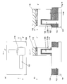
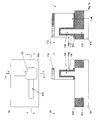
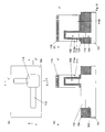
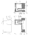
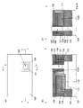
- FIG. 4B is a sectional view taken along line X-X ′ in FIG.
- FIG. 6C is a sectional view taken along line Y-Y ′ in FIG. (A) is a top view which concerns on the manufacturing method of the semiconductor device which concerns on this invention.
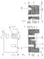
- FIG. 4B is a sectional view taken along line X-X ′ in FIG.
- FIG. 6C is a sectional view taken along line Y-Y ′ in FIG. (A) is a top view which concerns on the manufacturing method of the semiconductor device which concerns on this invention.
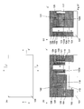
- FIG. 4B is a sectional view taken along line X-X ′ in FIG. FIG.
- FIG. 6C is a sectional view taken along line Y-Y ′ in FIG. (A) is a top view which concerns on the manufacturing method of the semiconductor device which concerns on this invention.
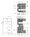
- FIG. 4B is a sectional view taken along line X-X ′ in FIG.
- FIG. 6C is a sectional view taken along line Y-Y ′ in FIG. (A) is a top view which concerns on the manufacturing method of the semiconductor device which concerns on this invention.
- FIG. 4B is a sectional view taken along line X-X ′ in FIG.
- FIG. 6C is a sectional view taken along line Y-Y ′ in FIG. (A) is a top view which concerns on the manufacturing method of the semiconductor device which concerns on this invention.
- FIG. 4B is a sectional view taken along line X-X ′ in FIG.
- FIG. 6C is a sectional view taken along line Y-Y ′ in FIG. (A) is a top view which concerns on the manufacturing method of the
- FIG. 4B is a sectional view taken along line X-X ′ in FIG.
- FIG. 6C is a sectional view taken along line Y-Y ′ in FIG. (A) is a top view which concerns on the manufacturing method of the semiconductor device which concerns on this invention.
- FIG. 4B is a sectional view taken along line X-X ′ in FIG.
- FIG. 6C is a sectional view taken along line Y-Y ′ in FIG. (A) is a top view which concerns on the manufacturing method of the semiconductor device which concerns on this invention.
- FIG. 4B is a sectional view taken along line X-X ′ in FIG.
- FIG. 6C is a sectional view taken along line Y-Y ′ in FIG.
- FIG. 4B is a sectional view taken along line X-X ′ in FIG.
- FIG. 6C is a sectional view taken along line Y-Y ′ in FIG. (A) is a top view which concerns on the manufacturing method of the semiconductor device which concerns on this invention.
- FIG. 4B is a sectional view taken along line X-X ′ in FIG.
- FIG. 6C is a sectional view taken along line Y-Y ′ in FIG. (A) is a top view which concerns on the manufacturing method of the semiconductor device which concerns on this invention.
- FIG. 4B is a sectional view taken along line X-X ′ in FIG. FIG.
- FIG. 6C is a sectional view taken along line Y-Y ′ in FIG. (A) is a top view which concerns on the manufacturing method of the semiconductor device which concerns on this invention.
- FIG. 4B is a sectional view taken along line X-X ′ in FIG.
- FIG. 6C is a sectional view taken along line Y-Y ′ in FIG. (A) is a top view which concerns on the manufacturing method of the semiconductor device which concerns on this invention.
- FIG. 4B is a sectional view taken along line X-X ′ in FIG.
- FIG. 6C is a sectional view taken along line Y-Y ′ in FIG. (A) is a top view which concerns on the manufacturing method of the semiconductor device which concerns on this invention.
- FIG. 4B is a sectional view taken along line X-X ′ in FIG.
- FIG. 6C is a sectional view taken along line Y-Y ′ in FIG. (A) is a top view which concerns on the manufacturing method of the
- FIG. 4B is a sectional view taken along line X-X ′ in FIG.
- FIG. 6C is a sectional view taken along line Y-Y ′ in FIG. (A) is a top view which concerns on the manufacturing method of the semiconductor device which concerns on this invention.
- FIG. 4B is a sectional view taken along line X-X ′ in FIG.
- FIG. 6C is a sectional view taken along line Y-Y ′ in FIG. (A) is a top view which concerns on the manufacturing method of the semiconductor device which concerns on this invention.
- FIG. 4B is a sectional view taken along line X-X ′ in FIG.
- FIG. 6C is a sectional view taken along line Y-Y ′ in FIG.
- FIG. 4B is a sectional view taken along line X-X ′ in FIG.
- FIG. 6C is a sectional view taken along line Y-Y ′ in FIG. (A) is a top view which concerns on the manufacturing method of the semiconductor device which concerns on this invention.
- FIG. 4B is a sectional view taken along line X-X ′ in FIG.
- FIG. 6C is a sectional view taken along line Y-Y ′ in FIG. (A) is a top view which concerns on the manufacturing method of the semiconductor device which concerns on this invention.
- FIG. 4B is a sectional view taken along line X-X ′ in FIG. FIG.
- FIG. 6C is a sectional view taken along line Y-Y ′ in FIG. (A) is a top view which concerns on the manufacturing method of the semiconductor device which concerns on this invention.
- FIG. 4B is a sectional view taken along line X-X ′ in FIG.
- FIG. 6C is a sectional view taken along line Y-Y ′ in FIG. (A) is a top view which concerns on the manufacturing method of the semiconductor device which concerns on this invention.
- FIG. 4B is a sectional view taken along line X-X ′ in FIG.
- FIG. 6C is a sectional view taken along line Y-Y ′ in FIG. (A) is a top view which concerns on the manufacturing method of the semiconductor device which concerns on this invention.
- FIG. 4B is a sectional view taken along line X-X ′ in FIG.
- FIG. 6C is a sectional view taken along line Y-Y ′ in FIG. (A) is a top view which concerns on the manufacturing method of the
- FIG. 4B is a sectional view taken along line X-X ′ in FIG.
- FIG. 6C is a sectional view taken along line Y-Y ′ in FIG. (A) is a top view which concerns on the manufacturing method of the semiconductor device which concerns on this invention.
- FIG. 4B is a sectional view taken along line X-X ′ in FIG.
- FIG. 6C is a sectional view taken along line Y-Y ′ in FIG. (A) is a top view which concerns on the manufacturing method of the semiconductor device which concerns on this invention.
- FIG. 4B is a sectional view taken along line X-X ′ in FIG.
- FIG. 6C is a sectional view taken along line Y-Y ′ in FIG.
- FIG. 4B is a sectional view taken along line X-X ′ in FIG.
- FIG. 6C is a sectional view taken along line Y-Y ′ in FIG. (A) is a top view which concerns on the manufacturing method of the semiconductor device which concerns on this invention.
- FIG. 4B is a sectional view taken along line X-X ′ in FIG.
- FIG. 6C is a sectional view taken along line Y-Y ′ in FIG. (A) is a top view which concerns on the manufacturing method of the semiconductor device which concerns on this invention.
- FIG. 4B is a sectional view taken along line X-X ′ in FIG. FIG.
- FIG. 6C is a sectional view taken along line Y-Y ′ in FIG. (A) is a top view which concerns on the manufacturing method of the semiconductor device which concerns on this invention.
- FIG. 4B is a sectional view taken along line X-X ′ in FIG.
- FIG. 6C is a sectional view taken along line Y-Y ′ in FIG. (A) is a top view which concerns on the manufacturing method of the semiconductor device which concerns on this invention.
- FIG. 4B is a sectional view taken along line X-X ′ in FIG.
- FIG. 6C is a sectional view taken along line Y-Y ′ in FIG. (A) is a top view which concerns on the manufacturing method of the semiconductor device which concerns on this invention.
- FIG. 4B is a sectional view taken along line X-X ′ in FIG.
- FIG. 6C is a sectional view taken along line Y-Y ′ in FIG. (A) is a top view which concerns on the manufacturing method of the
- FIG. 4B is a sectional view taken along line X-X ′ in FIG.
- FIG. 6C is a sectional view taken along line Y-Y ′ in FIG. (A) is a top view which concerns on the manufacturing method of the semiconductor device which concerns on this invention.
- FIG. 4B is a sectional view taken along line X-X ′ in FIG.
- FIG. 6C is a sectional view taken along line Y-Y ′ in FIG. (A) is a top view which concerns on the manufacturing method of the semiconductor device which concerns on this invention.
- FIG. 4B is a sectional view taken along line X-X ′ in FIG.
- FIG. 6C is a sectional view taken along line Y-Y ′ in FIG.
- FIG. 4B is a sectional view taken along line X-X ′ in FIG.
- FIG. 6C is a sectional view taken along line Y-Y ′ in FIG. (A) is a top view which concerns on the manufacturing method of the semiconductor device which concerns on this invention.
- FIG. 4B is a sectional view taken along line X-X ′ in FIG.
- FIG. 6C is a sectional view taken along line Y-Y ′ in FIG. (A) is a top view which concerns on the manufacturing method of the semiconductor device which concerns on this invention.
- FIG. 4B is a sectional view taken along line X-X ′ in FIG. FIG.
- FIG. 6C is a sectional view taken along line Y-Y ′ in FIG. (A) is a top view which concerns on the manufacturing method of the semiconductor device which concerns on this invention.
- FIG. 4B is a sectional view taken along line X-X ′ in FIG.
- FIG. 6C is a sectional view taken along line Y-Y ′ in FIG. (A) is a top view which concerns on the manufacturing method of the semiconductor device which concerns on this invention.
- FIG. 4B is a sectional view taken along line X-X ′ in FIG.
- FIG. 6C is a sectional view taken along line Y-Y ′ in FIG. (A) is a top view which concerns on the manufacturing method of the semiconductor device which concerns on this invention.
- FIG. 4B is a sectional view taken along line X-X ′ in FIG.
- FIG. 6C is a sectional view taken along line Y-Y ′ in FIG. (A) is a top view which concerns on the manufacturing method of the
- FIG. 4B is a sectional view taken along line X-X ′ in FIG.
- FIG. 6C is a sectional view taken along line Y-Y ′ in FIG. (A) is a top view which concerns on the manufacturing method of the semiconductor device which concerns on this invention.
- FIG. 4B is a sectional view taken along line X-X ′ in FIG.
- FIG. 6C is a sectional view taken along line Y-Y ′ in FIG. (A) is a top view which concerns on the manufacturing method of the semiconductor device which concerns on this invention.
- FIG. 4B is a sectional view taken along line X-X ′ in FIG.
- FIG. 6C is a sectional view taken along line Y-Y ′ in FIG.
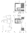
- a first resist for forming a fin-shaped semiconductor layer is formed on a semiconductor substrate, the semiconductor substrate is etched, the fin-shaped semiconductor layer is formed, the first resist is removed, and the fin-shaped semiconductor layer is removed.
- a first insulating film is deposited around the semiconductor layer, the first insulating film is etched back, an upper portion of the fin-like semiconductor layer is exposed, and a second resist is formed so as to be orthogonal to the fin-like semiconductor layer.
- Forming the columnar silicon layer by etching the fin-like semiconductor layer and removing the second resist so that the portion where the fin-like semiconductor layer and the second resist are orthogonal to each other becomes the columnar silicon layer.
- the 1st process of forming a semiconductor layer is shown. In this embodiment, silicon is used as the material for the semiconductor substrate, but a semiconductor material other than silicon can also be used.
- a first resist 102 for forming a fin-like silicon layer is formed on the silicon substrate 101.
- the silicon substrate 101 is etched to form a fin-like silicon layer 103.
- the fin-like silicon layer is formed using a resist as a mask this time, a hard mask such as an oxide film or a nitride film may be used as the mask.
- the first resist 102 is removed.
- a first insulating film 104 is deposited around the fin-like silicon layer 103.
- an oxide film formed by high-density plasma or an oxide film formed by low-pressure chemical vapor deposition may be used.
- the first insulating film 104 is etched back to expose the upper portion of the fin-like silicon layer 103.
- a second resist 105 is formed so as to be orthogonal to the fin-like silicon layer 103.
- a portion where the fin-like silicon layer 103 and the resist 105 are orthogonal to each other is a portion that becomes a columnar silicon layer. Since a line-shaped resist can be used, the possibility that the resist falls after patterning is low, and the process is stable.
- the fin-like silicon layer 103 is etched. A portion where the fin-like silicon layer 103 and the second resist 105 are orthogonally becomes the columnar silicon layer 106. Therefore, the width of the columnar silicon layer 106 is the same as the width of the fin-like silicon layer.
- a columnar silicon layer 106 is formed on the fin-shaped silicon layer 103, and a first insulating film 104 is formed around the fin-shaped silicon layer 103.
- the second resist 105 is removed.
- the first resist for forming the fin-like semiconductor layer is formed on the semiconductor substrate, the semiconductor substrate is etched, the fin-like semiconductor layer is formed, the first resist is removed, and the fin A first insulating film is deposited around the semiconductor layer, the first insulating film is etched back, an upper portion of the fin-like semiconductor layer is exposed, and a second insulating film is perpendicular to the fin-like semiconductor layer.
- the resist is formed, the fin-like semiconductor layer is etched, and the second resist is removed, so that the portion where the fin-like semiconductor layer and the second resist are orthogonal to each other becomes the columnar silicon layer.
- the first step of forming the columnar semiconductor layer is shown.
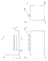
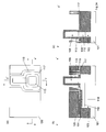
- a second insulating film is formed, polysilicon is deposited, and the upper surface of the polysilicon after planarizing the polysilicon is positioned higher than the second insulating film above the columnar semiconductor layer.
- Planarizing depositing a first nitride film, forming a third resist for forming a polysilicon gate electrode and polysilicon gate wiring, etching the first nitride film, etching the polysilicon; 2 shows a second step of forming the polysilicon gate electrode and the polysilicon gate wiring, etching the second insulating film, and removing the third resist.
- a second insulating film 113 is formed, and polysilicon 114 is deposited and planarized.
- the upper surface of the planarized polysilicon is higher than the second insulating film 113 above the columnar silicon layer 106.
- the second insulating film an oxide film or a thermal oxide film by deposition is preferable.
- a first nitride film 115 is deposited.
- the first nitride film 115 is a film that inhibits formation of silicide on the polysilicon gate electrode and the polysilicon gate wiring when the silicide is formed on the fin-like silicon layer.
- a third resist 116 for forming a polysilicon gate electrode and a polysilicon gate wiring is formed. It is desirable that a portion to be a gate wiring is orthogonal to the fin-like silicon layer 103. This is because the parasitic capacitance between the gate wiring and the substrate is reduced.
- the first nitride film 115 is etched.
- the polysilicon 114 is etched to form a polysilicon gate electrode 114a and a polysilicon gate wiring 114b.
- the second insulating film 113 is etched.
- the third resist 116 is removed.
- the second insulating film is formed, polysilicon is deposited, and the upper surface of the polysilicon after planarizing the polysilicon is positioned higher than the second insulating film above the columnar semiconductor layer.
- Planarizing depositing a first nitride film, forming a third resist for forming a polysilicon gate electrode and polysilicon gate wiring, etching the first nitride film, etching the polysilicon;
- the second step of forming the polysilicon gate electrode and the polysilicon gate wiring, etching the second insulating film, and removing the third resist is shown.
- an impurity such as arsenic or phosphorus is implanted for nMOS and boron or BF2 is implanted for pMOS, and heat treatment is performed, so that a diffusion layer 112 is formed above fin-shaped silicon layer 103 and columnar silicon layer 106. Form. At this time, since the upper part of the columnar silicon layer 106 is covered with the polysilicon gate electrode, no diffusion layer is formed.
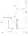
- a second nitride film is deposited, the second nitride film is etched, remains in a sidewall shape, a second metal is deposited, and a metal-semiconductor compound is deposited on the upper portion of the fin-like semiconductor layer.
- the 4th process formed in the upper part of a diffusion layer is shown.
- a second nitride film 117 is deposited.
- the second nitride film 117 is etched and left in a sidewall shape.
- a second metal such as nickel or cobalt is deposited, and a compound of metal and semiconductor, that is, silicide 118 is formed on the diffusion layer 112 above the fin-like silicon layer 103.
- the polysilicon gate electrode 114a and the polysilicon gate wiring 114b are covered with the second nitride film 117 and the first nitride film 115, and the upper part of the columnar silicon layer 106 is the second insulating film 113 and the polysilicon gate. Since it is covered with the electrode 114a and the polysilicon gate wiring 114b, no silicide is formed.
- the second nitride film is deposited, the second nitride film is etched, remains in the sidewall shape, the second metal is deposited, and the compound of the metal and the semiconductor is deposited on the upper part of the fin-shaped semiconductor layer.
- a fourth step of forming on the diffusion layer is shown.
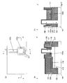
- a third nitride film is deposited, an interlayer insulating film is deposited and planarized, the polysilicon gate electrode and the polysilicon gate wiring are exposed, and the exposed second nitride film and third nitride film are exposed. Removing, removing the polysilicon gate electrode, the polysilicon gate wiring and the second insulating film, depositing a gate insulating film, and in the portion where the polysilicon gate electrode and the polysilicon gate wiring are present.
- a fifth step of embedding the metal, etching the first metal, exposing the gate insulating film above the columnar silicon layer, and forming a metal gate electrode and a metal gate wiring is shown.
- a third nitride film 119 is deposited to protect the silicide 118.
- an interlayer insulating film 120 is deposited and planarized by chemical mechanical polishing.
- the interlayer insulating film 120 is etched back to expose the second nitride film 115 and the third nitride film 119 covering the polysilicon gate electrode 114a and the polysilicon gate wiring 114b.
- the exposed second nitride film 115 and third nitride film 119 are removed, and the polysilicon gate electrode 114a and the polysilicon gate wiring 114b are exposed.
- the etching used for removing the second nitride film 115 and the third nitride film 119 is preferably isotropic etching or wet etching.
- the exposed polysilicon gate electrode 114a and polysilicon gate wiring 114b are removed.
- the etching at this time is also preferably isotropic etching or wet etching.
- the second insulating film 113 is removed.
- a gate insulating film 121 and a first metal 122 are deposited.
- the first metal 122 is buried in the portion where the polysilicon gate electrode 114a and the polysilicon gate wiring 114b exist. It is preferable to use atomic layer deposition for this embedding.
- As the gate insulating film 121 a film generally used in a semiconductor process such as an oxide film, an oxynitride film, and a high dielectric film can be used.
- the first metal 122 may be any metal that is used in a semiconductor process and sets a threshold voltage of a transistor. At this time, when the work function of the first metal 112 is between 4.2 eV and 5.0 eV, the first metal 112 can operate as an enhancement type.
- the first metal 122 is etched to expose the gate insulating film 121 on the columnar silicon layer 106. Thereby, the metal gate electrode 122a and the metal gate wiring 122b are formed.
- the third nitride film is deposited, the interlayer insulating film is deposited and planarized, the polysilicon gate electrode and the polysilicon gate wiring are exposed, and the exposed second nitride film and third nitride film are removed. Removing, removing the polysilicon gate electrode, the polysilicon gate wiring and the second insulating film, depositing a gate insulating film, and in the portion where the polysilicon gate electrode and the polysilicon gate wiring are present.
- the fifth step of embedding the metal, etching the first metal, exposing the gate insulating film above the columnar silicon layer, and forming the metal gate electrode and the metal gate wiring is shown.
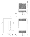
- an oxide film 123 is deposited.
- the oxide film 123 is etched back and left on the upper surface of the metal gate electrode 122a.
- the etching at this time is preferably isotropic etching.
- the upper part of the columnar silicon layer 106 is exposed.
- a third metal 124 is deposited.
- the work function of the third metal 124 is between 4.0 eV and 4.2 eV, it is in the vicinity of the work function of n-type silicon 4.05 eV, so that the upper part of the columnar silicon layer 106 functions as n-type silicon. To do.
- the third metal 124 at this time for example, a compound of tantalum and titanium (TaTi) or tantalum nitride (TaN) is preferable.
- the work function of the third metal 124 is between 5.0 eV and 5.2 eV
- the work function of the p-type silicon is in the vicinity of 5.15 eV, so that the upper part of the columnar silicon layer 106 functions as p-type silicon.
- the third metal 124 at this time for example, ruthenium (Ru) or titanium nitride (TiN) is preferable.
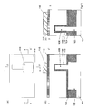
- the third metal 124 is etched to form a side wall made of the third metal 124 on the upper side wall of the columnar silicon layer 106.
- a side wall made of the third metal 124 is formed on the upper side wall of the columnar silicon layer 106 with the insulating film 121 interposed therebetween.
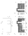
- the upper portion of the columnar semiconductor layer is exposed, the third metal is deposited, the third metal is etched, and a sidewall made of the third metal is formed on the upper sidewall of the columnar semiconductor layer.
- a sixth step was indicated.
- an interlayer insulating film 125 is deposited, planarized, and etched back to expose the upper surface of the columnar silicon layer 106 and the upper surface of the side wall made of the third metal 124.
- a fourth resist 126 for forming a contact hole is formed on the metal gate wiring 122b and on the fin-like silicon layer 103.
- the interlayer insulating films 120 and 125 and the oxide film 123 are etched to form contact holes 127 and 128.
- the fourth resist 126 is removed.
- the third nitride film 119 is etched to expose the silicide 118.
- metal 129 is deposited. Thereby, the contacts 130 and 131 are formed. At this time, the sidewall made of the third metal 124 and the upper surface of the columnar silicon layer 106 are connected. Therefore, the same potential is applied to the upper part of the columnar silicon layer 106 and the sidewall made of the third metal 124. In the upper part of the columnar silicon layer 106, carriers are induced by the work function difference between the third metal 124 and silicon.
- fifth resists 132, 133, and 134 for forming metal wiring are formed.
- the metal 129 is etched to form metal wirings 135, 136, and 137.
- the fifth resists 132, 133, and 134 are removed.
- a gate insulating film 121 formed around the columnar silicon layer 106 a metal gate electrode 122a formed around the gate insulating film 121, and a metal gate wiring 122b connected to the metal gate electrode 112a
- a side wall made of the third metal 124 formed on the upper side wall of the columnar silicon layer 106, A sidewall and the columnar silicon layer 106 top surface made of the third metal 124 is characterized in that it is connected.
- the diffusion layer is not formed on the upper part of the columnar silicon layer 106, and the upper part of the columnar silicon layer 106 can function as an n-type semiconductor layer or a p-type semiconductor layer depending on a work function difference between the metal and the semiconductor. Therefore, it is possible to reduce the step of forming the diffusion layer on the columnar silicon layer 106.
- the density of silicon is 5 ⁇ 10 22 pieces / cm 3 , so that it is difficult to make impurities exist in the silicon column. The problem can be avoided.
Landscapes
- Chemical & Material Sciences (AREA)
- Insulated Gate Type Field-Effect Transistor (AREA)
- Composite Materials (AREA)
- Engineering & Computer Science (AREA)
- Manufacturing & Machinery (AREA)
- Inorganic Chemistry (AREA)
- Electrodes Of Semiconductors (AREA)
Abstract
La présente invention a pour objectif de mettre à disposition un procédé de production de transistor à électrode de grille enveloppante (transistor SGT) qui est un procédé de grille en dernier et un transistor SGT ayant une structure amenant la partie supérieure d'une couche semi-conductrice en forme de pilier à fonctionner en tant que couche semi-conductrice de type n ou en tant que couche semi-conductrice de type p en se basant sur la différence de fonction de travail entre un métal et un semi-conducteur. Pour ce faire, le procédé de production de dispositif à semi-conducteurs comprend les étapes suivantes : formation d'un premier film isolant au niveau de la périphérie d'une couche semi-conductrice en forme d'ailette et formation d'une couche semi-conductrice en forme de pilier sur le sommet de la couche semi-conductrice en forme d'ailette; fabrication d'un second film isolant, d'une électrode de grille de polysilicium, et d'un fil de grille de polysilicium, l'électrode de grille de polysilicium enveloppant le second film isolant; formation d'une couche de diffusion dans la partie supérieure de la couche semi-conductrice en forme d'ailette et dans la partie inférieure de la couche silicone en forme de pilier; formation d'un composé de métal et de semi-conducteur dans la partie supérieure de la couche de diffusion sur le sommet de la couche semi-conductrice en forme d'ailette; dépôt d'un film isolant intercouche, exposition de l'électrode de grille de polysilicium et du fil de grille de polysilicium, gravure de l'électrode de grille de polysilicium et du fil de grille de polysilicium, puis dépôt d'un premier métal et formation d'une électrode de grille en métal et d'un fil de grille en métal; et formation d'une paroi latérale comprenant un troisième métal sur la paroi latérale de la partie supérieure de la couche semi-conductrice en forme de pilier. La paroi latérale comprenant le troisième métal et la surface supérieure de la couche semi-conductrice en forme de pilier sont connectées.
Priority Applications (4)
| Application Number | Priority Date | Filing Date | Title |
|---|---|---|---|
| JP2014521766A JP5670603B1 (ja) | 2013-04-26 | 2013-04-26 | 半導体装置の製造方法及び半導体装置 |
| PCT/JP2013/062423 WO2014174672A1 (fr) | 2013-04-26 | 2013-04-26 | Procédé de production de dispositif à semi-conducteurs, et dispositif à semi-conducteurs |
| US14/755,317 US9768267B2 (en) | 2013-04-26 | 2015-06-30 | Surrounding gate semiconductor device |
| US15/672,549 US9842902B1 (en) | 2013-04-26 | 2017-08-09 | Method for producing surrounding gate semiconductor device |
Applications Claiming Priority (1)
| Application Number | Priority Date | Filing Date | Title |
|---|---|---|---|
| PCT/JP2013/062423 WO2014174672A1 (fr) | 2013-04-26 | 2013-04-26 | Procédé de production de dispositif à semi-conducteurs, et dispositif à semi-conducteurs |
Related Child Applications (1)
| Application Number | Title | Priority Date | Filing Date |
|---|---|---|---|
| US14/755,317 Continuation US9768267B2 (en) | 2013-04-26 | 2015-06-30 | Surrounding gate semiconductor device |
Publications (1)
| Publication Number | Publication Date |
|---|---|
| WO2014174672A1 true WO2014174672A1 (fr) | 2014-10-30 |
Family
ID=51791276
Family Applications (1)
| Application Number | Title | Priority Date | Filing Date |
|---|---|---|---|
| PCT/JP2013/062423 Ceased WO2014174672A1 (fr) | 2013-04-26 | 2013-04-26 | Procédé de production de dispositif à semi-conducteurs, et dispositif à semi-conducteurs |
Country Status (3)
| Country | Link |
|---|---|
| US (2) | US9768267B2 (fr) |
| JP (1) | JP5670603B1 (fr) |
| WO (1) | WO2014174672A1 (fr) |
Cited By (1)
| Publication number | Priority date | Publication date | Assignee | Title |
|---|---|---|---|---|
| JP2020513160A (ja) * | 2017-04-17 | 2020-04-30 | インターナショナル・ビジネス・マシーンズ・コーポレーションInternational Business Machines Corporation | 半導体構造体の寄生容量を低減する方法および寄生容量を低減する半導体構造体 |
Families Citing this family (1)
| Publication number | Priority date | Publication date | Assignee | Title |
|---|---|---|---|---|
| JP5798276B1 (ja) * | 2014-06-16 | 2015-10-21 | ユニサンティス エレクトロニクス シンガポール プライベート リミテッドUnisantis Electronics Singapore Pte Ltd. | 半導体装置の製造方法、及び、半導体装置 |
Citations (3)
| Publication number | Priority date | Publication date | Assignee | Title |
|---|---|---|---|---|
| JP2003179132A (ja) * | 2001-12-10 | 2003-06-27 | Mitsubishi Electric Corp | 半導体装置およびその製造方法 |
| WO2009110050A1 (fr) * | 2008-02-15 | 2009-09-11 | 日本ユニサンティスエレクトロニクス株式会社 | Procédé de fabrication d'un dispositif semiconducteur |
| JP2010251678A (ja) * | 2009-04-20 | 2010-11-04 | Unisantis Electronics Japan Ltd | 半導体装置の製造方法 |
Family Cites Families (19)
| Publication number | Priority date | Publication date | Assignee | Title |
|---|---|---|---|---|
| JP2703970B2 (ja) | 1989-01-17 | 1998-01-26 | 株式会社東芝 | Mos型半導体装置 |
| JP3057661B2 (ja) | 1988-09-06 | 2000-07-04 | 株式会社東芝 | 半導体装置 |
| JP2950558B2 (ja) | 1989-11-01 | 1999-09-20 | 株式会社東芝 | 半導体装置 |
| JPH11297984A (ja) | 1998-04-07 | 1999-10-29 | Seiko Epson Corp | Ldd型mosトランジスタの構造および形成方法 |
| US6891234B1 (en) | 2004-01-07 | 2005-05-10 | Acorn Technologies, Inc. | Transistor with workfunction-induced charge layer |
| JP4108537B2 (ja) | 2003-05-28 | 2008-06-25 | 富士雄 舛岡 | 半導体装置 |
| JP2005268418A (ja) * | 2004-03-17 | 2005-09-29 | Fujio Masuoka | 半導体記憶装置及びその製造方法 |
| JP2006310651A (ja) * | 2005-04-28 | 2006-11-09 | Toshiba Corp | 半導体装置の製造方法 |
| JP2008066562A (ja) * | 2006-09-08 | 2008-03-21 | Toshiba Corp | 半導体装置およびその製造方法 |
| JP2008218514A (ja) * | 2007-02-28 | 2008-09-18 | Toshiba Corp | 磁気ランダムアクセスメモリ及びその製造方法 |
| JP5466816B2 (ja) * | 2007-08-09 | 2014-04-09 | ピーエスフォー ルクスコ エスエイアールエル | 縦型mosトランジスタの製造方法 |
| JP2009081163A (ja) * | 2007-09-25 | 2009-04-16 | Elpida Memory Inc | 半導体装置およびその製造方法 |
| US8163605B2 (en) | 2008-02-15 | 2012-04-24 | Unisantis Electronics Singapore Pte Ltd. | Production method for semiconductor device |
| JP4487221B1 (ja) | 2009-04-17 | 2010-06-23 | 日本ユニサンティスエレクトロニクス株式会社 | 半導体装置 |
| US20160336400A1 (en) * | 2011-11-09 | 2016-11-17 | Unisantis Electronics Singapore Pte. Ltd. | Semiconductor device |
| US8697511B2 (en) * | 2012-05-18 | 2014-04-15 | Unisantis Electronics Singapore Pte. Ltd. | Method for producing semiconductor device and semiconductor device |
| US8877578B2 (en) * | 2012-05-18 | 2014-11-04 | Unisantis Electronics Singapore Pte. Ltd. | Method for producing semiconductor device and semiconductor device |
| JP5798276B1 (ja) * | 2014-06-16 | 2015-10-21 | ユニサンティス エレクトロニクス シンガポール プライベート リミテッドUnisantis Electronics Singapore Pte Ltd. | 半導体装置の製造方法、及び、半導体装置 |
| WO2016013087A1 (fr) * | 2014-07-24 | 2016-01-28 | ユニサンティス エレクトロニクス シンガポール プライベート リミテッド | Procédé de fabrication de dispositif à semi-conducteur et dispositif à semi-conducteur |
-
2013
- 2013-04-26 WO PCT/JP2013/062423 patent/WO2014174672A1/fr not_active Ceased
- 2013-04-26 JP JP2014521766A patent/JP5670603B1/ja active Active
-
2015
- 2015-06-30 US US14/755,317 patent/US9768267B2/en active Active
-
2017
- 2017-08-09 US US15/672,549 patent/US9842902B1/en active Active
Patent Citations (3)
| Publication number | Priority date | Publication date | Assignee | Title |
|---|---|---|---|---|
| JP2003179132A (ja) * | 2001-12-10 | 2003-06-27 | Mitsubishi Electric Corp | 半導体装置およびその製造方法 |
| WO2009110050A1 (fr) * | 2008-02-15 | 2009-09-11 | 日本ユニサンティスエレクトロニクス株式会社 | Procédé de fabrication d'un dispositif semiconducteur |
| JP2010251678A (ja) * | 2009-04-20 | 2010-11-04 | Unisantis Electronics Japan Ltd | 半導体装置の製造方法 |
Cited By (2)
| Publication number | Priority date | Publication date | Assignee | Title |
|---|---|---|---|---|
| JP2020513160A (ja) * | 2017-04-17 | 2020-04-30 | インターナショナル・ビジネス・マシーンズ・コーポレーションInternational Business Machines Corporation | 半導体構造体の寄生容量を低減する方法および寄生容量を低減する半導体構造体 |
| JP7062682B2 (ja) | 2017-04-17 | 2022-05-06 | インターナショナル・ビジネス・マシーンズ・コーポレーション | 半導体構造体の寄生容量を低減する方法および寄生容量を低減する半導体構造体 |
Also Published As
| Publication number | Publication date |
|---|---|
| US9842902B1 (en) | 2017-12-12 |
| US20170338320A1 (en) | 2017-11-23 |
| JPWO2014174672A1 (ja) | 2017-02-23 |
| US9768267B2 (en) | 2017-09-19 |
| US20150295057A1 (en) | 2015-10-15 |
| JP5670603B1 (ja) | 2015-02-18 |
Similar Documents
| Publication | Publication Date | Title |
|---|---|---|
| US8772175B2 (en) | Method for manufacturing semiconductor device and semiconductor device | |
| JP5695745B2 (ja) | 半導体装置の製造方法及び半導体装置 | |
| US8916478B2 (en) | Method for manufacturing semiconductor device and semiconductor device | |
| WO2013093988A1 (fr) | Procédé de production de dispositif semi-conducteur, et dispositif semi-conducteur | |
| US10008595B2 (en) | Method for producing semiconductor device and semiconductor device | |
| WO2013080378A1 (fr) | Dispositif à semi-conducteurs, et procédé de fabrication de celui-ci | |
| US20140203353A1 (en) | Method for manufacturing semiconductor device and semiconductor device | |
| WO2013171873A1 (fr) | Dispositif à semi-conducteurs | |
| JP5670603B1 (ja) | 半導体装置の製造方法及び半導体装置 | |
| JP5740535B1 (ja) | 半導体装置の製造方法、及び、半導体装置 | |
| JP6368836B2 (ja) | 半導体装置の製造方法、及び、半導体装置 | |
| JP6143913B2 (ja) | 半導体装置の製造方法及び半導体装置 | |
| JP5917673B2 (ja) | 半導体装置の製造方法及び半導体装置 | |
| JP6329301B2 (ja) | 半導体装置の製造方法及び半導体装置 | |
| JP6284585B2 (ja) | 半導体装置の製造方法及び半導体装置 | |
| JP6326437B2 (ja) | 半導体装置の製造方法、及び、半導体装置 | |
| JP5890053B2 (ja) | 半導体装置の製造方法、及び、半導体装置 | |
| JP6156883B2 (ja) | 半導体装置の製造方法及び半導体装置 | |
| JP6080989B2 (ja) | 半導体装置の製造方法、及び、半導体装置 | |
| JP5869166B2 (ja) | 半導体装置の製造方法、及び、半導体装置 |
Legal Events
| Date | Code | Title | Description |
|---|---|---|---|
| ENP | Entry into the national phase |
Ref document number: 2014521766 Country of ref document: JP Kind code of ref document: A |
|
| 121 | Ep: the epo has been informed by wipo that ep was designated in this application |
Ref document number: 13883307 Country of ref document: EP Kind code of ref document: A1 |
|
| NENP | Non-entry into the national phase |
Ref country code: DE |
|
| 122 | Ep: pct application non-entry in european phase |
Ref document number: 13883307 Country of ref document: EP Kind code of ref document: A1 |