WO2014181569A1 - Appareil d'antenne - Google Patents
Appareil d'antenne Download PDFInfo
- Publication number
- WO2014181569A1 WO2014181569A1 PCT/JP2014/055350 JP2014055350W WO2014181569A1 WO 2014181569 A1 WO2014181569 A1 WO 2014181569A1 JP 2014055350 W JP2014055350 W JP 2014055350W WO 2014181569 A1 WO2014181569 A1 WO 2014181569A1
- Authority
- WO
- WIPO (PCT)
- Prior art keywords
- frequency band
- resonance circuit
- low frequency
- resonance
- variable
- Prior art date
- Legal status (The legal status is an assumption and is not a legal conclusion. Google has not performed a legal analysis and makes no representation as to the accuracy of the status listed.)
- Ceased
Links
Images


Classifications
-
- H—ELECTRICITY
- H01—ELECTRIC ELEMENTS
- H01Q—ANTENNAS, i.e. RADIO AERIALS
- H01Q5/00—Arrangements for simultaneous operation of antennas on two or more different wavebands, e.g. dual-band or multi-band arrangements
- H01Q5/30—Arrangements for providing operation on different wavebands
- H01Q5/307—Individual or coupled radiating elements, each element being fed in an unspecified way
- H01Q5/314—Individual or coupled radiating elements, each element being fed in an unspecified way using frequency dependent circuits or components, e.g. trap circuits or capacitors
- H01Q5/328—Individual or coupled radiating elements, each element being fed in an unspecified way using frequency dependent circuits or components, e.g. trap circuits or capacitors between a radiating element and ground
-
- H—ELECTRICITY
- H01—ELECTRIC ELEMENTS
- H01Q—ANTENNAS, i.e. RADIO AERIALS
- H01Q1/00—Details of, or arrangements associated with, antennas
- H01Q1/12—Supports; Mounting means
- H01Q1/22—Supports; Mounting means by structural association with other equipment or articles
- H01Q1/24—Supports; Mounting means by structural association with other equipment or articles with receiving set
- H01Q1/241—Supports; Mounting means by structural association with other equipment or articles with receiving set used in mobile communications, e.g. GSM
- H01Q1/242—Supports; Mounting means by structural association with other equipment or articles with receiving set used in mobile communications, e.g. GSM specially adapted for hand-held use
- H01Q1/243—Supports; Mounting means by structural association with other equipment or articles with receiving set used in mobile communications, e.g. GSM specially adapted for hand-held use with built-in antennas
-
- H—ELECTRICITY
- H01—ELECTRIC ELEMENTS
- H01Q—ANTENNAS, i.e. RADIO AERIALS
- H01Q5/00—Arrangements for simultaneous operation of antennas on two or more different wavebands, e.g. dual-band or multi-band arrangements
- H01Q5/30—Arrangements for providing operation on different wavebands
- H01Q5/307—Individual or coupled radiating elements, each element being fed in an unspecified way
- H01Q5/314—Individual or coupled radiating elements, each element being fed in an unspecified way using frequency dependent circuits or components, e.g. trap circuits or capacitors
- H01Q5/335—Individual or coupled radiating elements, each element being fed in an unspecified way using frequency dependent circuits or components, e.g. trap circuits or capacitors at the feed, e.g. for impedance matching
-
- H—ELECTRICITY
- H01—ELECTRIC ELEMENTS
- H01Q—ANTENNAS, i.e. RADIO AERIALS
- H01Q5/00—Arrangements for simultaneous operation of antennas on two or more different wavebands, e.g. dual-band or multi-band arrangements
- H01Q5/30—Arrangements for providing operation on different wavebands
- H01Q5/307—Individual or coupled radiating elements, each element being fed in an unspecified way
- H01Q5/342—Individual or coupled radiating elements, each element being fed in an unspecified way for different propagation modes
- H01Q5/357—Individual or coupled radiating elements, each element being fed in an unspecified way for different propagation modes using a single feed point
- H01Q5/364—Creating multiple current paths
- H01Q5/371—Branching current paths
-
- H—ELECTRICITY
- H03—ELECTRONIC CIRCUITRY
- H03H—IMPEDANCE NETWORKS, e.g. RESONANT CIRCUITS; RESONATORS
- H03H7/00—Multiple-port networks comprising only passive electrical elements as network components
- H03H7/38—Impedance-matching networks
- H03H7/40—Automatic matching of load impedance to source impedance
Definitions
- the present invention relates to an antenna device that operates in at least two frequency bands on the low frequency side and a high frequency band having a higher frequency.
- Patent Document 1 discloses a multiband antenna device. This antenna device has a reactance variable part and a matching part. The reactance variable unit is connected in series to the radiating element, and the matching unit is shunt-connected between the feeding circuit and the reactance variable unit. Both the reactance variable section and the matching section are configured by a parallel resonant circuit of an inductor and a capacitor.
- Impedance matching is performed by the matching unit.
- the radiating element in one band selected from a plurality of operating bands (bands) by changing the resonance frequency of the reactance variable unit.
- the return loss of the radiating element becomes large, and it is difficult to perform an efficient operation.
- the resonance frequency of the reactance variable unit is changed in order to switch the low frequency band. And that influence reaches the high frequency band. Thereby, the impedance matching in a high frequency band may collapse.
- An object of the present invention is to provide an antenna device capable of continuing operation in a high frequency band even when a low frequency band is switched.
- a radiating element operating in a first low frequency band, a second low frequency band higher than the first low frequency band, and a high frequency band higher than the second low frequency band;
- a ground conductor ;
- a variable resonance circuit inserted between a feeding point of the radiating element and the ground conductor and capable of switching between at least two first resonance characteristics and second resonance characteristics;
- the variable resonance circuit When the variable resonance circuit is in an open state where it is not inserted between the feeding point and the ground conductor, the input impedance of the radiating element is lower than 50 ⁇ in the first low frequency band and is capacitive.
- variable resonance circuit When the variable resonance circuit exhibits the first resonance characteristic, the variable resonance circuit is inductive in the first low frequency band, and the impedance of the variable resonance circuit in the high frequency band is the first resonance frequency. Higher than the impedance of the variable resonant circuit in the low frequency band of When the variable resonance circuit exhibits the second resonance characteristic, the variable resonance circuit is capacitive in the second low frequency band, and the impedance of the variable resonance circuit in the high frequency band is the second resonance frequency. An antenna device higher than the impedance of the variable resonance circuit in the low frequency band is provided.
- variable resonance circuit When the variable resonance circuit exhibits the first resonance characteristic, impedance matching is improved in the first low frequency band. When the variable resonance circuit exhibits the second resonance characteristic, impedance matching is improved in the second low frequency band. In any state, the impedance matching state in the high frequency band can be maintained.
- the input impedance of the radiating element when the variable resonance circuit exhibits the first resonance characteristic is 50 ⁇ than the input impedance of the radiating element in the open state.
- the input impedance of the radiating element when the variable resonant circuit exhibits the second resonance characteristic is 50 ⁇ than the input impedance of the radiating element in the open state. It is preferable to have a close configuration.
- the return loss of the radiating element in the high frequency band is greater than the return loss of the radiating element in the first low frequency band and the second low frequency band.
- a small configuration is preferable.
- the impedance matching be taken without inserting the variable resonance circuit.
- the first low frequency band ranges from 704 MHz to 787 MHz
- the second low frequency band ranges from 824 MHz to 960 MHz
- the high frequency band ranges from 1710 MHz to 2690 MHz. It is a range.
- the variable resonance circuit is A first resonance circuit exhibiting the first resonance characteristic; A second resonance circuit exhibiting the second resonance characteristic; A switch that switches between a state in which the first resonance circuit is inserted and a state in which the second resonance circuit is inserted between a feeding point of the radiating element and the ground conductor; Is possible.
- One of the first resonance circuit and the second resonance circuit is constituted by an LC series resonance circuit, and the other is constituted by an LC series resonance circuit or an LC parallel resonance circuit.
- the variable resonance circuit includes an inductor and a variable capacitor connected in series with each other, and the first resonance characteristic and the second resonance characteristic are switched by changing the capacitance of the variable capacitor. It is also possible.
- a sensor for detecting an approach of an object that affects a radiation characteristic of the radiation element It is good also as a structure which has a control circuit which changes the capacitance of the said variable capacitor based on the detection result of the said sensor.
- a configuration having a matching transformer inserted between the radiating element and the feeding point may be employed.
- variable resonance circuit When the variable resonance circuit exhibits the first resonance characteristic, impedance matching is improved in the first low frequency band. When the variable resonance circuit exhibits the second resonance characteristic, impedance matching is improved in the second low frequency band. In any state, the impedance matching state in the high frequency band can be maintained.
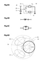
- FIGS. 1A is an equivalent circuit diagram of the antenna device to be evaluated, and FIGS. 1B and 1C are a graph and an admittance chart showing measurement results of the frequency characteristics of the return loss of the antenna device of FIG. 1A, respectively.
- 2A is an equivalent circuit diagram of the antenna device to be evaluated, and FIGS. 2B and 2C are a graph and an admittance chart showing measurement results of frequency characteristics of the return loss of the antenna device of FIG. 2A, respectively.
- 3A is an equivalent circuit diagram of the antenna device to be evaluated, and FIGS. 3B and 3C are a graph and an admittance chart showing measurement results of the frequency characteristics of the return loss of the antenna device of FIG. 3A, respectively.
- 4A is an equivalent circuit diagram of the antenna device to be evaluated, and FIGS.
- FIG. 4B and 4C are a graph and an admittance chart showing measurement results of the frequency characteristics of the return loss of the antenna device of FIG. 4A, respectively.
- FIG. 5A is an equivalent circuit diagram of the antenna device to be evaluated
- FIGS. 5B and 5C are a graph and an admittance chart showing measurement results of the frequency characteristics of the return loss of the antenna device of FIG. 5A, respectively.
- 6A is an equivalent circuit diagram of the antenna device according to the first embodiment
- FIGS. 6B and 6C are equivalent circuit diagrams of an LC series resonance circuit and an LC parallel resonance circuit applied to the variable resonance circuit, respectively. These are a Smith chart which shows the input impedance of the antenna apparatus by Example 1.
- FIG. 7A to 7D are graphs showing examples of resonance characteristics of the variable resonance circuit.
- FIG. 8 is a perspective view of the antenna device according to the first embodiment.
- FIG. 9 is a plan view of a variable resonance circuit of the antenna device according to the first embodiment.
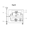
- FIG. 10 is an equivalent circuit diagram of the antenna device according to the second embodiment.
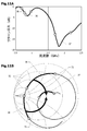
- FIG. 11A and FIG. 11B are a graph and an admittance chart showing the simulation results of the frequency characteristics of the return loss in the state where the variable resonance circuit is not inserted, respectively.
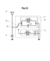
- FIG. 12 is an equivalent circuit diagram of the antenna device according to the second embodiment in a state where the first resonance circuit is shunt-connected.
- 13A and 13B are a graph and an admittance chart showing simulation results of the frequency characteristics of the return loss in the state shown in FIG. 12, respectively.
- FIG. 12 is an equivalent circuit diagram of the antenna device according to the second embodiment in a state where the first resonance circuit is shunt-connected.
- 13A and 13B are a graph and an admittance chart showing simulation results of the frequency characteristics of the return loss in the state shown in FIG
- FIG. 14 is an equivalent circuit diagram of the antenna device according to the second embodiment in a state where the second resonance circuit is shunt-connected.
- FIG. 15A and FIG. 15B are a graph and an admittance chart showing simulation results of the frequency characteristics of the return loss in the state shown in FIG.
- FIG. 16A is an equivalent circuit diagram of the antenna device according to the third embodiment
- FIG. 16B is an antenna device equivalent circuit diagram according to a modification of the third embodiment.
- FIG. 17 is an equivalent circuit diagram of the antenna device according to the third embodiment in a state where the first resonance circuit is shunt-connected.
- 18A and 18B are a graph and a admittance chart showing the simulation result of the frequency characteristics of the return loss in the state shown in FIG. 17, respectively.
- FIG. 17 is an equivalent circuit diagram of the antenna device according to the third embodiment in a state where the first resonance circuit is shunt-connected.
- 18A and 18B are a graph and a admittance chart showing the simulation result of the frequency characteristics of the return
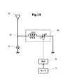
- FIG. 19 is an equivalent circuit diagram of the antenna device according to the fourth embodiment.
- FIG. 20 is an equivalent circuit diagram of the antenna device according to the fifth embodiment.
- FIG. 21A is an equivalent circuit diagram of an antenna device according to a reference example, and FIGS. 21B and 21C are a graph and an admittance chart showing simulation results of frequency characteristics of the return loss of the antenna device shown in FIG. 21A, respectively.
- 22A is an equivalent circuit diagram of the antenna device according to the reference example, and FIGS. 22B and 22C are a graph and an admittance chart showing the simulation result of the frequency characteristics of the return loss of the antenna device shown in FIG. 22A, respectively.
- 23A is an equivalent circuit diagram of an antenna device according to a reference example, and FIGS.
- FIGS. 23B and 23C are a graph and an admittance chart showing simulation results of frequency characteristics of return loss of the antenna device shown in FIG. 23A, respectively.
- 24A is an equivalent circuit diagram of the antenna device according to the fifth embodiment in a state where the variable resonance circuit is not shunt-connected
- FIGS. 24B and 24C are graphs of the frequency characteristics of the return loss of the antenna device shown in FIG. 24A, respectively. It is the graph which shows a simulation result, and an admittance chart.
- 25A is an equivalent circuit diagram of the antenna device according to the fifth embodiment in a state where the variable resonance circuit is an inductance.
- FIGS. 25B and 25C are simulation results of the frequency characteristics of the return loss of the antenna device shown in FIG. 25A, respectively.
- FIG. 26A is an equivalent circuit diagram of the antenna device according to the fifth embodiment in a state where the variable resonance circuit is an inductance.
- FIGS. 26B and 26C are simulation results of the frequency characteristics of the return loss of the antenna device shown in FIG. 26A, respectively. It is the graph which shows, and an admittance chart.
- the multiband antenna device in order to evaluate the influence of the switching of the band in the low frequency band on the high frequency band, various antenna devices were manufactured and the antenna characteristics were measured. Hereinafter, the results of this evaluation experiment will be described before describing the examples.
- FIG. 1A shows an equivalent circuit diagram of the antenna device to be evaluated.
- High frequency power is supplied from the power feeding circuit 31 to the radiating element 30.
- a branched monopole antenna was employed as the radiating element 30 as the radiating element 30, a branched monopole antenna was employed. This branched monopole antenna is designed so that matching can be achieved without a matching circuit in a high frequency band.
- FIG. 1B shows the measurement result of the frequency characteristics of the return loss of the radiating element 30.
- the horizontal axis represents frequency in the unit “MHz”, and the vertical axis represents return loss.
- One scale on the vertical axis corresponds to 5 dB.
- the numbers with circles shown in FIG. 1B indicate the lower limit frequency and the upper limit frequency of the operating frequency band.
- Point 1 and point 2 indicate the frequencies 704 MHz and 784 MHz, respectively, and correspond to the lower limit frequency and the upper limit frequency of the band including the band 17 and the band 13.
- Points 3 and 4 indicate 824 MHz and 960 MHz, respectively, and correspond to the lower limit frequency and the upper limit frequency of the band including band 5 and band 8.
- Points 5 and 6 indicate frequencies 1710 MHz and 2170 MHz, respectively, and correspond to the lower limit frequency and the upper limit frequency of the band including band 1 and band 3.
- a band from 704 MHz to 784 MHz including the band 17 and the band 13 is referred to as a “first low frequency band”, and a band from 824 MHz to 960 MHz including the band 5 and the band 8 is referred to as a “second frequency band”.
- the band from 1710 MHz to 2170 MHz including band 1 and band 3 is referred to as a “high frequency band”. It can be seen that the return loss is small and matching is achieved in the high frequency band.
- FIG. 1C shows a locus on the admittance chart of the input impedance of the radiating element 30.
- a constant conductance circle 32 and a constant susceptance circle 33 are drawn.
- the upper half region of the admittance chart corresponds to inductive impedance, and the lower half corresponds to capacitive impedance.
- a constant resistance circle 34 of 50 ⁇ is shown.
- the inside of the constant resistance circle 34 corresponds to an input impedance larger than 50 ⁇ , and the outside of the constant resistance circle 34 corresponds to an input impedance smaller than 50 ⁇ .
- the input impedance in the first low frequency band 35 is smaller than 50 ⁇ and is capacitive.
- the input impedance in the second low frequency band 36 is less than 50 ⁇ and is inductive.
- the locus of input impedance in the high frequency band is located near the center of the admittance chart. That is, impedance matching is taken in the high frequency band.
- a shunt inductor 40 is connected between the feeding point 38 of the radiating element 30 and the ground.
- the shunt inductor 40 has an inductance of 6.8 nH.
- FIG. 2B shows the measurement result of the frequency characteristics of the return loss of the radiating element 30 shown in FIG. 2A
- FIG. 2C shows the locus on the admittance chart of the input impedance of the radiating element 30 shown in FIG. 2A.
- the return loss in the high frequency band 37 is larger than that when the shunt inductor 40 is not connected, but is kept at a sufficiently small value. For this reason, even if the shunt inductor 40 is connected, the operation in the high frequency band 37 is possible. This is because the impedance of the shunt inductor 40 becomes sufficiently large in the high frequency band 37.
- a shunt capacitor 41 is connected between the feeding point 38 of the radiating element 30 and the ground.
- the capacitance of the shunt capacitor 41 is 2 pF.
- FIG. 3B shows the measurement result of the frequency characteristics of the return loss of the radiating element 30 shown in FIG. 3A
- FIG. 3C shows the locus on the admittance chart of the input impedance of the radiating element 30 shown in FIG. 3A.
- the impedance of the shunt capacitor 41 approaches zero. That is, the state is almost the same as the state where the feeding point 38 is grounded. For this reason, in the high frequency band 37, the input impedance of the radiation element 30 becomes remarkably small (in the admittance chart, a point indicating the input impedance approaches the outer peripheral line). Since impedance matching in the high frequency band 37 is lost, the return loss increases as shown in FIG. 3B.
- the antenna apparatus shown in FIGS. 2A to 2C was operable in both the first low frequency band 35 and the high frequency band 37.
- the antenna apparatus shown in FIGS. 3A to 3C can operate in the second low frequency band 36 but is difficult to operate in the high frequency band 37.
- the LC series resonance circuit 42 is shunt-connected between the feeding point 38 of the radiating element 30 and the ground.
- the inductance of the LC series resonant circuit 42 is 18 nH, and the capacitance is 3.2 pF.
- the LC series resonance circuit 42 is equivalent to an inductance of 6.8 nH at about 740 MHz which is the center frequency of the first low frequency band 35. That is, at 740 MHz, the antenna device of FIG. 4A is equivalent to the antenna device of FIG. 2A.
- the reactance of the LC series resonance circuit 42 is larger than the reactance at 740 MHz in a frequency band higher than 740 MHz.
- FIG. 4B shows the measurement result of the frequency characteristics of the return loss of the radiating element 30 shown in FIG. 4A
- FIG. 4C shows the locus on the admittance chart of the input impedance of the radiating element 30 shown in FIG. 4A. Since the LC series resonance circuit 42 shunt-connected to the feeding point 38 of the radiating element 30 exhibits inductive impedance at a frequency higher than the first low frequency band 35, the point indicating the input impedance at each frequency is As indicated by the arrow, the susceptance moves along the constant conductance circle 32 in the direction of decreasing. For this reason, the input impedance in the first low frequency band 35 approaches 50 ⁇ (approaches the center of the admittance chart). Thereby, as shown in FIG. 4B, the return loss in the first low frequency band 35 is reduced.
- the impedance of the LC series resonance circuit 42 is larger than the impedance of the shunt inductor 40 shown in FIG. 2A. For this reason, the impedance matching collapse in the high frequency band 37 is lighter than that of the antenna apparatus shown in FIG. 2A. For this reason, a sufficiently small return loss is maintained in the high frequency band 37.
- the shunt inductor 40 FIG. 2A
- the LC series resonance circuit 42 By replacing the shunt inductor 40 (FIG. 2A) with the LC series resonance circuit 42, the deterioration of the antenna characteristics in the high frequency band 37 can be reduced.
- an LC series resonance circuit 43 is shunt-connected between the feeding point 38 of the radiating element 30 and the ground.
- the inductance of the LC series resonance circuit 43 is 18 nH, and the capacitance is 0.8 pF.
- the LC series resonance circuit 43 exhibits a capacitance of 2 pF at about 880 MHz which is the center frequency of the second low frequency band 36. That is, at 880 MHz, the antenna device of FIG. 5A is equivalent to the antenna device of FIG. 3A.
- the impedance of the LC series resonance circuit 43 becomes inductive in a frequency range higher than the resonance frequency 1326 MHz.
- FIG. 5B shows the measurement result of the frequency characteristics of the return loss of the radiating element 30 shown in FIG. 5A
- FIG. 5C shows the locus on the admittance chart of the input impedance of the radiating element 30 shown in FIG. 5A. Since the LC series resonance circuit 43 shunt-connected to the feeding point 38 of the radiating element 30 exhibits capacitive impedance in the second low frequency band 36, the point indicating the input impedance at each frequency is in the constant conductance circle 32. Along the direction along which the susceptance increases. For this reason, the input impedance in the second low frequency band 36 approaches 50 ⁇ (approaches the center of the admittance chart). Thereby, as shown in FIG. 5B, the return loss in the second low frequency band 36 is reduced.
- the impedance of the shunt capacitor 41 of the antenna device of FIG. 3A approaches 0, but the LC series resonance circuit 43 of the antenna device of FIG. 5A exhibits inductive impedance at a frequency equal to or higher than the resonance frequency. As the value increases, the impedance increases. In the high frequency band 37, the LC series resonance circuit 43 exhibits a sufficiently large impedance, so that the matching condition in the high frequency band 37 is not significantly broken. For this reason, the antenna apparatus shown in FIG. 5A can also operate in the high frequency band 37.
- the operating frequency band of the antenna device is switched between the first low frequency band 35 and the second low frequency band 36. In either case of switching to the first low frequency band 35 or the second low frequency band 36, the operation in the high frequency band is possible.
- FIG. 6A shows an equivalent circuit diagram of the antenna device according to the first embodiment.
- the feeding circuit 31 supplies high-frequency power to the feeding point 38 of the radiating element 30.
- This antenna device is designed to operate in a first low frequency band (for example, 704 MHz to 784 MHz), a second low frequency band (824 MHz to 960 MHz), and a high frequency band (1710 MHz to 2170 MHz).
- a variable resonance circuit 50 is inserted (shunted) between the feeding point 38 and the ground.
- the variable resonance circuit 50 can switch the resonance characteristics between at least two first resonance characteristics and second resonance characteristics.
- the variable resonance circuit 50 includes a first resonance circuit 51 that exhibits first resonance characteristics, a second resonance circuit 52 that exhibits second resonance characteristics, and a switch 53.
- the switch 53 for example, a single pole double throw switch (SPDT switch) is used. The switch 53 switches between a state in which the first resonance circuit 51 is inserted and a state in which the second resonance circuit 52 is inserted between the feeding point 38 and the ground.
- SPDT switch single pole double throw switch
- One of the first resonance circuit 51 and the second resonance circuit 52 is configured by the LC series resonance circuit shown in FIG. 6B, and the other is the LC series resonance circuit shown in FIG. 6B or the LC parallel resonance shown in FIG. 6C. It consists of a circuit.
- the input impedance of the radiating element 30 will be described with reference to the Smith chart (impedance chart) shown in FIG. 6D.
- the input impedance of the radiating element 30 is lower than 50 ⁇ in the first low frequency band 35 and is capacitive. That is, the point indicating the input impedance of the radiating element 30 is located outside the 50 ⁇ constant resistance circle 56 and in the lower half of the Smith chart. For example, the point indicating the input impedance of the radiating element 30 in the first low-frequency band 35 is located in the region 57 shown in FIG. 6D.
- the input impedance of the radiating element 30 When the variable resonance circuit 50 is in an open state where it is not inserted between the feeding point 38 and the ground, the input impedance of the radiating element 30 is lower than 50 ⁇ in the second low frequency band 36 and is capacitive. That is, the point indicating the input impedance of the radiating element 30 is located outside the 50 ⁇ constant resistance circle 56 and in the upper half region of the Smith chart. For example, the point indicating the input impedance of the radiating element 30 in the second low frequency band 36 is located in the region 58 shown in FIG. 6D.
- the input impedance of the radiating element 30 is closer to 50 ⁇ than the input impedance in the first low frequency band 35 and the second low frequency band 36.
- the point indicating the input impedance in the high frequency band 37 of the radiating element 30 is located in a region closer to the center 55 of the Smith chart than the regions 57 and 58 illustrated in FIG. 6D.
- the point indicating the input impedance in the high frequency band 37 is located in a region 59 including the center 55.
- FIG. 7A and 7B show an example of the resonance characteristics of the first resonance circuit 51 (FIG. 6A).
- the horizontal axis represents frequency, the vertical axis represents reactance, and the origin corresponds to the resonance frequency.
- the resonance characteristics shown in FIG. 7A are realized by an LC series resonance circuit (FIG. 6B), and the resonance characteristics shown in FIG. 7B are realized by an LC parallel resonance circuit (FIG. 6C).
- the first resonant circuit 51 exhibits inductive impedance in the first low frequency band 35 and exhibits higher impedance in the high frequency band 37 than the impedance in the first low frequency band 35.
- the input impedance of the radiating element 30 approaches the center 55 from the region 57 (FIG. 6D). For this reason, impedance matching can be improved in the first low frequency band 35. In the high frequency band 37, since the first resonance circuit 51 exhibits a large impedance, the impedance matching state is maintained.
- the resonance frequency is lower than the first low frequency band 35 as shown in FIG. 7A.
- the impedance in the high frequency band 37 is always higher than the impedance in the first low frequency band 35.
- the resonance frequency is higher than that of the first low frequency band 35 as shown in FIG. 7B.
- the impedance gradually approaches 0 ⁇ as the frequency increases.
- the first frequency is set so that the resonance frequency is located in the vicinity of the high frequency band 37 or inside the high frequency band 37.
- a resonant circuit 51 is designed.
- FIG. 7C shows an example of the resonance characteristics of the second resonance circuit 52.
- the horizontal axis represents frequency, the vertical axis represents reactance, and the origin corresponds to the resonance frequency.
- the resonance characteristics shown in FIG. 7C are realized by an LC series resonance circuit (FIG. 6B).
- the second resonant circuit 52 exhibits capacitive impedance in the second low frequency band 36 and exhibits higher impedance in the high frequency band 37 than in the second low frequency band 36.
- the input impedance of the radiating element 30 approaches the center 55 from the region 58 (FIG. 6D). For this reason, impedance matching can be improved in the second low frequency band 36. In the high frequency band 37, since the second resonance circuit 52 exhibits a large impedance, the impedance matching state is maintained.
- FIG. 7D shows the resonance characteristics of the LC parallel resonance circuit.
- the resonant frequency In order for the LC parallel resonant circuit to be capacitive in the second low frequency band 36, the resonant frequency must be lower than that of the second low frequency band 36. At this time, in the frequency band higher than the second low frequency band 36, the impedance of the LC parallel resonant circuit approaches 0 ⁇ than the impedance in the second low frequency band 36. For this reason, in the high frequency band 37, the condition that the impedance is higher than the impedance in the second low frequency band 36 cannot be satisfied. Therefore, the second resonance circuit 52 cannot be configured with an LC parallel resonance circuit.
- the antenna device when the first resonance circuit 51 is selected by the switch 53, the antenna device is in a state where impedance matching is achieved in the first low frequency band 35 and the high frequency band 37.
- the antenna device When the second resonance circuit 52 is selected by the switch 53, the antenna device is in a state where impedance matching is achieved in the second low frequency band 36 and the high frequency band 37.
- FIG. 8 shows a schematic perspective view of the antenna device according to the first embodiment.
- This antenna device is mounted on, for example, a portable wireless terminal.
- the radiating element 30 is disposed in the vicinity of one edge of the rectangular ground conductor 60.
- a substrate for forming the ground conductor 60 for example, a dielectric substrate such as glass epoxy is used. Conductive films are formed on both surfaces of the dielectric substrate, and the conductive films on both surfaces are connected to each other through a plurality of through holes formed in the dielectric substrate.
- This conductive film constitutes the ground conductor 60.
- ABS resin is used for the dielectric carrier for forming the radiating element 30.
- the radiation element 30 includes a high-frequency radiation element 30A and a low-frequency radiation element 30B.
- the radiating element 30 has a branched monopole antenna structure.
- another antenna that operates in a plurality of bands of a low frequency band and a high frequency band may be used.
- a variable resonance circuit 50 is disposed in the vicinity of the feeding point 38 of the radiating element 30.
- the low-frequency radiating element 30B is preferably extended in a direction away from the ground conductor 60, and the length thereof is preferably 1 ⁇ 4 of the wavelength of the operating frequency.
- the low-frequency radiating element 30 ⁇ / b> B is often disposed along one edge of the ground conductor 60.
- the stray capacitance between the low-frequency radiating element 30B and the ground conductor 60 increases. For this reason, input impedance becomes small in a low frequency band, and it becomes difficult to perform impedance matching without a matching circuit.
- the high-frequency radiating element 30A is shorter than the low-frequency radiating element 30B, it is easy to obtain impedance matching without a matching circuit.
- impedance matching is performed in the first low frequency band or the second low frequency band by shunt connection of the variable resonance circuit 50.
- impedance matching is performed without a matching circuit.
- FIG. 9 shows a plan view of the variable resonance circuit 50.
- the feed point 38 of the radiating element 30 is connected to one of the first resonance circuit 51 and the second resonance circuit 52 by a switch 53 (FIG. 6A).
- the first transmission line 61 connects the first resonance circuit 51 and the ground point 65.
- the second transmission line 62 connects the second resonance circuit 52 and the ground point 65.
- the ground point 65 is connected to a conductive film (ground conductor) on the back surface through a through hole formed in the dielectric substrate.
- the second transmission line 62 connected to the second resonance circuit 52 has a structure equivalent to an open stub.
- the first transmission line 61 connected to the first resonance circuit 51 has a structure equivalent to an open stub.
- these stub-like patterns extend from the ground point 65, the antenna characteristics are not easily affected by unnecessary resonance caused by the stub-like patterns.
- variable resonance circuit 50 is arranged between the vicinity of the feeding point 38 having a relatively low potential compared to the middle of the radiating element 30 in the length direction and the ground. For this reason, it is possible to prevent an excessively high voltage from being applied to the inductor, capacitor, switch, and the like that constitute the variable resonance circuit 50.
- FIG. 10 shows an equivalent circuit diagram of the antenna device according to the second embodiment.
- the first resonance circuit 51 (FIG. 6A) according to the first embodiment is configured by a parallel resonance circuit of a 6.7 nH inductor and a 1.2 pF capacitor
- the second resonance circuit 52 ( FIG. 6A) is composed of a series resonant circuit of an 18 nH inductor and a 0.8 pF capacitor.
- FIG. 11A shows a simulation result of the frequency characteristics of the return loss of the radiating element 30 when the variable resonance circuit 50 is not inserted between the feeding point 38 and the ground.
- the impedance is not matched when the variable resonance circuit 50 (FIG. 10) is not inserted, so that the return loss is large.
- the high frequency band 37 since impedance matching is achieved even when the variable resonance circuit 50 (FIG. 10) is not inserted, the return loss is sufficiently small.
- FIG. 11B shows a locus on the admittance chart of the input impedance of the radiating element 30 in the open state.
- Points 1 and 2 indicate the lower limit value and the upper limit value of the frequency of the first low frequency band 35, respectively.
- Points 3 and 4 indicate the lower limit value and the upper limit value of the frequency of the second low frequency band 36, respectively.
- Points 5 and 6 indicate a lower limit value and an upper limit value of the frequency of the high frequency band 37, respectively.
- the input impedance of the radiating element 30 is greater than 50 ⁇ and is capacitive.
- the input impedance of the radiating element 30 is simply referred to as “input impedance”.
- the input impedance in the second low frequency band 36 is less than 50 ⁇ and is inductive.
- the input impedance in the high frequency band 37 is closer to 50 ⁇ (center of the admittance chart) than the input impedance in the first low frequency band 35 and the second low frequency band 36.
- the point corresponding to the input impedance moves on the admittance chart along the constant conductance circle 32 in a direction in which the susceptance decreases, as indicated by an arrow 71. Thereby, the input impedance in the first low frequency band 35 can be brought close to 50 ⁇ .
- the point corresponding to the input impedance moves on the admittance chart along the constant conductance circle 32 in the direction of increasing the susceptance as indicated by an arrow 72.
- the input impedance in the second low frequency band 36 can be close to 50 ⁇ .
- the simulation result of the return loss when the first resonance circuit 51 is inserted between the feeding point 38 and the ground by the switch 53, and the locus of the input impedance on the admittance chart are shown in FIGS. 13A and 13B, respectively.
- the first resonance circuit 51 exhibits inductive impedance in the first low frequency band 35.
- the point indicating the input impedance in the first low frequency band 35 moves in the direction of the arrow 71. That is, the input impedance approaches 50 ⁇ . Since the impedance matching of the radiating element 30 is improved in the first low frequency band 35, the return loss in the first low frequency band 35 is reduced.
- the impedance of the first resonance circuit 51 is sufficiently high in the high frequency band 37, so that the impedance matching state in the high frequency band is maintained.
- the second resonant circuit 52 exhibits capacitive impedance in the second low frequency band 36.
- the point indicating the input impedance in the second low frequency band 36 moves in the direction of the arrow 72. That is, the input impedance approaches 50 ⁇ . Since the impedance matching of the radiating element 30 is improved in the second low frequency band 36, the return loss in the second low frequency band 36 is reduced.
- the impedance of the second resonance circuit 52 is sufficiently high in the high frequency band 37, so that the impedance matching state in the high frequency band is maintained.
- FIG. 16A shows an equivalent circuit diagram of the antenna device according to the third embodiment.
- the first resonant circuit 51 (FIG. 6A) according to the first embodiment is configured by a series resonant circuit including an 18 nH inductor and a 3.8 pF capacitor.
- the second resonance circuit 52 (FIG. 6A) includes a series resonance circuit of an 18 nH inductor and a 0.8 pF capacitor.
- one of the first resonant circuit 51 and the second resonant circuit 52 is configured by an LC series resonant circuit, and the other is configured by an LC parallel resonant circuit. It consists of a series resonant circuit.
- an 18 nH inductor may be shared by the first resonance circuit 51 and the second resonance circuit 52 to switch between a 0.8 pF capacitor and a 3.8 pF capacitor.
- FIG. 17 the simulation result of the return loss when the first resonance circuit 51 is shunt-connected to the feeding point 38 by the switch 53, and the locus of the input impedance on the admittance chart are shown in FIG. 18A and FIG. 18B, respectively. Shown in The first resonance circuit 51 exhibits inductive impedance in the first low frequency band 35.
- the point indicating the input impedance in the first low frequency band 35 approaches the center of the admittance chart, that is, 50 ⁇ . Since impedance matching is improved in the first low frequency band 35, the return loss is reduced in the first low frequency band 35 as shown in FIG. 18A. Further, in the high frequency band 37, the first resonant circuit 51 exhibits a large impedance, so that the impedance matching condition is hardly affected. For this reason, a state in which impedance matching is achieved in the high frequency band 37 is maintained.
- FIG. 19 shows an equivalent circuit diagram of the antenna device according to the fourth embodiment.
- the variable resonance circuit 50 is configured by a series resonance circuit of a fixed inductor and a variable capacitor. By changing the capacitance of the variable capacitor, the resonance characteristic of the variable resonance circuit can be switched between the first resonance characteristic and the second resonance characteristic.
- the inductance of the fixed inductor is 18 nH, for example.
- the capacitance of the variable capacitor is adjusted to 3.8 pF, the same state as when the first resonance circuit 51 (FIG. 17) of the third embodiment is shunt-connected to the feeding point 38 is realized.
- the capacitance of the variable capacitor is adjusted to 0.8 pF, the same state as that in which the second resonance circuit 52 (FIG. 17) of the third embodiment is shunt-connected to the feeding point 38 is realized.
- the antenna device further includes a sensor 75 and a control circuit 76.
- the sensor 75 detects the approach of an object that affects the radiation characteristics of the radiating element 30, such as a human body or a conductor.
- the detection result by the sensor 75 is given to the control circuit 76.
- the control circuit 76 changes the capacitance of the variable capacitor based on the detection result of the sensor 75. Thereby, it is possible to compensate for the collapse of the impedance matching state due to the approach of the human body or the conductor and maintain the matching state.
- FIG. 20 shows an equivalent circuit diagram of the antenna device according to the fifth embodiment.
- a matching transformer 77 is inserted between the feeding point 38 and the radiating element 30.
- Other configurations are the same as those of the antenna device according to the first embodiment shown in FIG. 6A.
- the antenna device according to the reference example will be described with reference to FIGS. 21A to 23C.
- FIG. 21A shows an equivalent circuit diagram of the antenna device with no matching circuit inserted.
- High frequency power is supplied from the power feeding circuit 31 to the radiating element 30.
- FIGS. 21B and 21C show the simulation results of the frequency characteristics of the return loss of the radiating element 30 shown in FIG. 21A and the locus of the input impedance on the admittance chart. Since no matching circuit is inserted, impedance matching is not achieved in the first low frequency band 35 and the second low frequency band 36. That is, as shown in FIG. 21B, the return loss is large, and as shown in FIG. 21C, the point indicating the input impedance is located in a region far from the center of the admittance chart. Although not shown in FIGS. 21B and 21C, impedance matching is taken in the high frequency band 37 (for example, FIG. 11A).
- FIG. 22A the simulation result of the return loss when the 5.1 nH shunt inductor is inserted and the locus of the input impedance in the admittance chart are shown in FIG. 22B and FIG. 22C, respectively.
- Impedance matching is improved in the first low frequency band 35 by inserting a 5.1 nH shunt inductor.
- the return loss in the vicinity of 787 MHz which is the upper limit value of the frequency of the first low frequency band 35 is larger than the return loss in the vicinity of 704 MHz which is the lower limit value. That is, it cannot be said that a sufficiently low return loss is obtained in the entire first low frequency band 35.
- FIG. 23A the simulation result of the return loss when a 6 pF shunt capacitor is inserted and the locus of the input impedance in the admittance chart are shown in FIG. 23B and FIG. 23C, respectively.
- Impedance matching is improved in the second low frequency band 36 by inserting a 6 pF shunt capacitor.
- the return loss in the vicinity of 824 MHz that is the lower limit value of the frequency of the second low frequency band 36 is larger than the return loss in the vicinity of 960 MHz that is the upper limit value. That is, it cannot be said that a sufficiently low return loss is obtained in the entire second low frequency band 36.
- the vicinity of the upper limit value of the frequency of the first low-frequency band 35 and the second low-frequency band, which are difficult to improve impedance matching with only the shunt inductor and the shunt capacitor, are described. Even in the vicinity of the lower limit of 36 frequencies, the impedance matching can be sufficiently improved.
- the operation and effect of the antenna device according to the fifth embodiment will be described with reference to FIGS. 24A to 26C.
- FIG. 24A the simulation results of the return loss when the variable resonance circuit 50 is not inserted between the feeding point 38 and the ground, and the locus of the input impedance in the admittance chart are shown in FIGS. 24B and 24C, respectively. Show.
- the broken line shown in FIG. 24C indicates the locus of input impedance when the radiating element 30 side is viewed from the feeding point 38 when the variable resonance circuit 50 is not inserted between the feeding point 38 and the ground.
- the inductance connected to the radiating element 30 is 60 nH
- the inductance connected to the feeding point 38 is 120 nH. That is, the transformer ratio is 1: 2. Since the variable resonance circuit 50 is not inserted, impedance matching is not achieved in the first low frequency band 35 and the second low frequency band 36.
- the locus of the input impedance when the radiating element 30 is viewed from the feeding point 38 moves to the right on the admittance chart.
- FIG. 25A the simulation results of the return loss when an 11 nH inductor (shunt inductor) is connected to the position of the variable resonance circuit 50 and the locus of the input impedance on the admittance chart are shown in FIGS. 25B and 25C, respectively. Show. Impedance matching is improved in the first low frequency band 35.
- the point 2 corresponding to the upper limit value of the frequency of the first low frequency band 35 is moved to the right on the admittance chart by connecting the matching transformer, and further, the constant conductance circle 32 is connected by connecting the shunt inductor. Along the direction of decreasing susceptance. Therefore, the input impedance in the vicinity of the upper limit value of the frequency of the first low frequency band 35 can be made sufficiently close to 50 ⁇ .
- FIG. 26A the simulation result of the return loss when a 3.5 pF capacitor (shunt capacitor) is connected to the position of the variable resonance circuit 50, and the locus of the input impedance on the admittance chart are shown in FIG. 26B and FIG. Shown in 26C. Impedance matching is improved in the second low frequency band 36.
- the point 3 corresponding to the lower limit value of the frequency of the second low frequency band 36 moves to the right on the admittance chart by connecting a matching transformer, and further, by connecting a shunt capacitor, a constant conductance circle 32 is obtained.
- the input impedance in the vicinity of the lower limit value of the frequency of the second low frequency band 36 can be made sufficiently close to 50 ⁇ .
Landscapes
- Engineering & Computer Science (AREA)
- Computer Networks & Wireless Communication (AREA)
- Details Of Aerials (AREA)
Abstract
Selon la présente invention, un circuit de résonance variable est inséré entre un conducteur de mise à la terre et le point d'alimentation d'un élément de rayonnement. Lorsque le circuit de résonance variable n'est pas inséré, l'impédance d'entrée de l'élément de rayonnement est inférieure à 50 Ω et est capacitive dans une première bande de basse fréquence, est inférieure à 50 Ω et est inductive dans une seconde bande de basse fréquence, et présente une valeur proche de 50 Ω dans une bande de haute fréquence. Lorsque le circuit de résonance variable affiche une première caractéristique de résonance, le circuit de résonance variable est inductif dans la première bande de basse fréquence, et l'impédance dans la bande de haute fréquence est supérieure à l'impédance dans la première bande de basse fréquence. Lorsque le circuit de résonance variable affiche une seconde caractéristique de résonance, le circuit de résonance variable est capacitif dans la seconde bande de basse fréquence, et l'impédance dans la bande de haute fréquence est supérieure à l'impédance dans la seconde bande de basse fréquence.
Priority Applications (1)
| Application Number | Priority Date | Filing Date | Title |
|---|---|---|---|
| US14/887,411 US9634390B2 (en) | 2013-05-10 | 2015-10-20 | Antenna device |
Applications Claiming Priority (2)
| Application Number | Priority Date | Filing Date | Title |
|---|---|---|---|
| JP2013-100156 | 2013-05-10 | ||
| JP2013100156 | 2013-05-10 |
Related Child Applications (1)
| Application Number | Title | Priority Date | Filing Date |
|---|---|---|---|
| US14/887,411 Continuation US9634390B2 (en) | 2013-05-10 | 2015-10-20 | Antenna device |
Publications (1)
| Publication Number | Publication Date |
|---|---|
| WO2014181569A1 true WO2014181569A1 (fr) | 2014-11-13 |
Family
ID=51867055
Family Applications (1)
| Application Number | Title | Priority Date | Filing Date |
|---|---|---|---|
| PCT/JP2014/055350 Ceased WO2014181569A1 (fr) | 2013-05-10 | 2014-03-04 | Appareil d'antenne |
Country Status (2)
| Country | Link |
|---|---|
| US (1) | US9634390B2 (fr) |
| WO (1) | WO2014181569A1 (fr) |
Cited By (4)
| Publication number | Priority date | Publication date | Assignee | Title |
|---|---|---|---|---|
| CN109638455A (zh) * | 2018-12-12 | 2019-04-16 | 维沃移动通信有限公司 | 天线结构及通信终端 |
| US10424841B2 (en) | 2015-07-31 | 2019-09-24 | Murata Manufacturing Co., Ltd. | Antenna matching circuit, antenna circuit, front-end circuit, and communication apparatus |
| CN111431518A (zh) * | 2020-04-21 | 2020-07-17 | 珠海复旦创新研究院 | 一种新型数控双频射频开关 |
| WO2021090487A1 (fr) * | 2019-11-08 | 2021-05-14 | ソニー株式会社 | Circuit d'adaptation et dispositif d'antenne |
Families Citing this family (17)
| Publication number | Priority date | Publication date | Assignee | Title |
|---|---|---|---|---|
| JP6212405B2 (ja) * | 2014-02-19 | 2017-10-11 | シャープ株式会社 | 無線機 |
| US10290940B2 (en) * | 2014-03-19 | 2019-05-14 | Futurewei Technologies, Inc. | Broadband switchable antenna |
| EP3159966B1 (fr) * | 2014-08-08 | 2020-04-22 | Huawei Technologies Co. Ltd. | Dispositif d'antenne et terminal |
| US10381717B2 (en) * | 2017-03-17 | 2019-08-13 | Nxp B.V. | Automotive antenna |
| CN117318668A (zh) | 2017-05-24 | 2023-12-29 | 安乐泰克有限公司 | 用于控制谐振器的装置和方法 |
| CN107967026B (zh) * | 2017-11-23 | 2019-10-25 | Oppo广东移动通信有限公司 | 天线组件、终端设备及改善天线辐射性能的方法 |
| JP6741189B1 (ja) * | 2018-09-07 | 2020-08-19 | 株式会社村田製作所 | アンテナ素子、アンテナモジュールおよび通信装置 |
| US11277110B2 (en) | 2019-09-03 | 2022-03-15 | Anlotek Limited | Fast frequency switching in a resonant high-Q analog filter |
| JP2023504732A (ja) | 2019-12-05 | 2023-02-06 | アンロテック リミテッド | 周波数合成における安定した調整可能なアクティブフィードバックアナログフィルタの使用 |
| EP3890189A1 (fr) | 2020-03-30 | 2021-10-06 | Anlotek Limited | Filtres analogiques de rétroaction active avec résonateurs couplés |
| EP3926828A1 (fr) | 2020-06-15 | 2021-12-22 | Anlotek Limited | Filtre passe-bande réglable à haute stabilité et réglage orthogonal |
| CN112397902B (zh) * | 2020-10-23 | 2023-06-20 | Oppo广东移动通信有限公司 | 一种天线及其阻抗匹配方法、终端 |
| CN114447574B (zh) * | 2020-11-04 | 2025-02-25 | 富泰京精密电子(烟台)有限公司 | 天线结构及具有该天线结构的无线通信装置 |
| US11955942B2 (en) | 2021-02-27 | 2024-04-09 | Anlotek Limited | Active multi-pole filter |
| EP4084333A1 (fr) | 2021-04-30 | 2022-11-02 | Anlotek Limited | Réduction du bruit de phase dans un résonateur rf analogique variable à condensateurs à valeur fixe et commutables |
| EP4089920A1 (fr) | 2021-05-12 | 2022-11-16 | Anlotek Limited | Commutation de fréquence rapide dans un filtre rf variable |
| TWI793867B (zh) * | 2021-11-19 | 2023-02-21 | 啓碁科技股份有限公司 | 通訊裝置 |
Citations (4)
| Publication number | Priority date | Publication date | Assignee | Title |
|---|---|---|---|---|
| JPS63177622A (ja) * | 1986-11-14 | 1988-07-21 | Seiko Epson Corp | アンテナ回路 |
| JP2002076750A (ja) * | 2000-08-24 | 2002-03-15 | Murata Mfg Co Ltd | アンテナ装置およびそれを備えた無線機 |
| WO2011024280A1 (fr) * | 2009-08-27 | 2011-03-03 | 株式会社 東芝 | Dispositif dantenne et dispositif de communication |
| JP2011155626A (ja) * | 2009-12-28 | 2011-08-11 | Fujitsu Ltd | アンテナ装置及び通信装置 |
Family Cites Families (11)
| Publication number | Priority date | Publication date | Assignee | Title |
|---|---|---|---|---|
| US6670924B1 (en) * | 2000-04-13 | 2003-12-30 | Mitsubishi Denki Kabushiki Kaisha | Antenna element and portable information terminal |
| JP2003249811A (ja) * | 2001-12-20 | 2003-09-05 | Murata Mfg Co Ltd | 複共振アンテナ装置 |
| JP4132016B2 (ja) | 2001-12-25 | 2008-08-13 | 松下電器産業株式会社 | 整合回路およびプラズマ処理装置 |
| JP2005311762A (ja) * | 2004-04-22 | 2005-11-04 | Matsushita Electric Ind Co Ltd | 可変整合回路 |
| JP4959956B2 (ja) | 2005-06-07 | 2012-06-27 | 株式会社日立製作所 | アンテナ |
| EP2104178A4 (fr) * | 2007-01-19 | 2014-05-28 | Murata Manufacturing Co | Module d'antenne et dispositif de communication sans fil |
| JP2009278192A (ja) * | 2008-05-12 | 2009-11-26 | Sony Ericsson Mobilecommunications Japan Inc | アンテナ装置及び通信端末装置 |
| JP5304890B2 (ja) | 2009-04-01 | 2013-10-02 | 株式会社村田製作所 | アンテナ整合回路、アンテナ装置及びアンテナ装置の設計方法 |
| CN102474005B (zh) * | 2010-01-19 | 2015-07-15 | 株式会社村田制作所 | 稳频电路、稳频器件、天线装置、及通信终端设备 |
| CN102484497B (zh) * | 2010-08-11 | 2014-06-04 | 株式会社村田制作所 | 稳频电路、天线装置、及通信终端设备 |
| CN103141031B (zh) * | 2011-02-23 | 2015-05-20 | 株式会社村田制作所 | 阻抗变换电路以及通信终端装置 |
-
2014
- 2014-03-04 WO PCT/JP2014/055350 patent/WO2014181569A1/fr not_active Ceased
-
2015
- 2015-10-20 US US14/887,411 patent/US9634390B2/en active Active
Patent Citations (4)
| Publication number | Priority date | Publication date | Assignee | Title |
|---|---|---|---|---|
| JPS63177622A (ja) * | 1986-11-14 | 1988-07-21 | Seiko Epson Corp | アンテナ回路 |
| JP2002076750A (ja) * | 2000-08-24 | 2002-03-15 | Murata Mfg Co Ltd | アンテナ装置およびそれを備えた無線機 |
| WO2011024280A1 (fr) * | 2009-08-27 | 2011-03-03 | 株式会社 東芝 | Dispositif dantenne et dispositif de communication |
| JP2011155626A (ja) * | 2009-12-28 | 2011-08-11 | Fujitsu Ltd | アンテナ装置及び通信装置 |
Cited By (6)
| Publication number | Priority date | Publication date | Assignee | Title |
|---|---|---|---|---|
| US10424841B2 (en) | 2015-07-31 | 2019-09-24 | Murata Manufacturing Co., Ltd. | Antenna matching circuit, antenna circuit, front-end circuit, and communication apparatus |
| CN109638455A (zh) * | 2018-12-12 | 2019-04-16 | 维沃移动通信有限公司 | 天线结构及通信终端 |
| WO2020119349A1 (fr) * | 2018-12-12 | 2020-06-18 | 维沃移动通信有限公司 | Structure d'antenne et terminal de communication |
| US11967780B2 (en) | 2018-12-12 | 2024-04-23 | Vivo Mobile Communication Co., Ltd. | Antenna structure and communications terminal |
| WO2021090487A1 (fr) * | 2019-11-08 | 2021-05-14 | ソニー株式会社 | Circuit d'adaptation et dispositif d'antenne |
| CN111431518A (zh) * | 2020-04-21 | 2020-07-17 | 珠海复旦创新研究院 | 一种新型数控双频射频开关 |
Also Published As
| Publication number | Publication date |
|---|---|
| US20160043468A1 (en) | 2016-02-11 |
| US9634390B2 (en) | 2017-04-25 |
Similar Documents
| Publication | Publication Date | Title |
|---|---|---|
| WO2014181569A1 (fr) | Appareil d'antenne | |
| US20140306855A1 (en) | Tunable multiband antenna | |
| CN101111972B (zh) | 天线及无线通信设备 | |
| US9190721B2 (en) | Antenna device | |
| JP6838631B2 (ja) | アンテナ装置および通信端末装置 | |
| JP5790869B2 (ja) | アンテナ装置 | |
| CN105789831A (zh) | 移动终端及其天线结构 | |
| TWI502817B (zh) | 通訊裝置 | |
| US20120032862A1 (en) | Antenna arrangement, dielectric substrate, pcb & device | |
| US8207895B2 (en) | Shorted monopole antenna | |
| US9142888B2 (en) | Antenna-device substrate and antenna device | |
| WO2021036753A1 (fr) | Antenne et dispositif électronique | |
| WO2010050278A1 (fr) | Dispositif de radiocommunication | |
| JPWO2015182677A1 (ja) | マルチアンテナ及びそれを備える無線装置 | |
| JP6015944B2 (ja) | アンテナ装置、通信装置、及び電子機器 | |
| JP5998974B2 (ja) | アンテナ | |
| US8081128B2 (en) | Antenna device and wireless communication apparatus | |
| US12412979B2 (en) | Antenna device and communication terminal apparatus | |
| CN104604025A (zh) | 用于可调谐天线的方法和装置 | |
| JP5994500B2 (ja) | 結合度調整素子、アンテナ装置および無線通信装置 | |
| JPWO2015033632A1 (ja) | インピーダンス変換回路、アンテナ装置および無線通信装置 | |
| TW201347297A (zh) | 無線裝置之天線 | |
| WO2016076120A1 (fr) | Dispositif d'antennes et dispositif de communication | |
| KR101931146B1 (ko) | 소형 광대역 안테나 | |
| CN103731176B (zh) | 通信装置 |
Legal Events
| Date | Code | Title | Description |
|---|---|---|---|
| 121 | Ep: the epo has been informed by wipo that ep was designated in this application |
Ref document number: 14795083 Country of ref document: EP Kind code of ref document: A1 |
|
| NENP | Non-entry into the national phase |
Ref country code: DE |
|
| 122 | Ep: pct application non-entry in european phase |
Ref document number: 14795083 Country of ref document: EP Kind code of ref document: A1 |
|
| NENP | Non-entry into the national phase |
Ref country code: JP |