WO2014196235A1 - Dispositif d'éclairage, dispositif d'affichage et dispositif de réception de télévision - Google Patents
Dispositif d'éclairage, dispositif d'affichage et dispositif de réception de télévision Download PDFInfo
- Publication number
- WO2014196235A1 WO2014196235A1 PCT/JP2014/055025 JP2014055025W WO2014196235A1 WO 2014196235 A1 WO2014196235 A1 WO 2014196235A1 JP 2014055025 W JP2014055025 W JP 2014055025W WO 2014196235 A1 WO2014196235 A1 WO 2014196235A1
- Authority
- WO
- WIPO (PCT)
- Prior art keywords
- light
- guide plate
- light guide
- light incident
- adjacent end
- Prior art date
- Legal status (The legal status is an assumption and is not a legal conclusion. Google has not performed a legal analysis and makes no representation as to the accuracy of the status listed.)
- Ceased
Links
Images




Classifications
-
- G—PHYSICS
- G02—OPTICS
- G02F—OPTICAL DEVICES OR ARRANGEMENTS FOR THE CONTROL OF LIGHT BY MODIFICATION OF THE OPTICAL PROPERTIES OF THE MEDIA OF THE ELEMENTS INVOLVED THEREIN; NON-LINEAR OPTICS; FREQUENCY-CHANGING OF LIGHT; OPTICAL LOGIC ELEMENTS; OPTICAL ANALOGUE/DIGITAL CONVERTERS
- G02F1/00—Devices or arrangements for the control of the intensity, colour, phase, polarisation or direction of light arriving from an independent light source, e.g. switching, gating or modulating; Non-linear optics
- G02F1/01—Devices or arrangements for the control of the intensity, colour, phase, polarisation or direction of light arriving from an independent light source, e.g. switching, gating or modulating; Non-linear optics for the control of the intensity, phase, polarisation or colour
- G02F1/13—Devices or arrangements for the control of the intensity, colour, phase, polarisation or direction of light arriving from an independent light source, e.g. switching, gating or modulating; Non-linear optics for the control of the intensity, phase, polarisation or colour based on liquid crystals, e.g. single liquid crystal display cells
- G02F1/133—Constructional arrangements; Operation of liquid crystal cells; Circuit arrangements
- G02F1/1333—Constructional arrangements; Manufacturing methods
- G02F1/1335—Structural association of cells with optical devices, e.g. polarisers or reflectors
- G02F1/1336—Illuminating devices
- G02F1/133615—Edge-illuminating devices, i.e. illuminating from the side
-
- H—ELECTRICITY
- H04—ELECTRIC COMMUNICATION TECHNIQUE
- H04N—PICTORIAL COMMUNICATION, e.g. TELEVISION
- H04N5/00—Details of television systems
- H04N5/64—Constructional details of receivers, e.g. cabinets or dust covers
-
- G—PHYSICS
- G02—OPTICS
- G02B—OPTICAL ELEMENTS, SYSTEMS OR APPARATUS
- G02B6/00—Light guides; Structural details of arrangements comprising light guides and other optical elements, e.g. couplings
- G02B6/0001—Light guides; Structural details of arrangements comprising light guides and other optical elements, e.g. couplings specially adapted for lighting devices or systems
- G02B6/0011—Light guides; Structural details of arrangements comprising light guides and other optical elements, e.g. couplings specially adapted for lighting devices or systems the light guides being planar or of plate-like form
- G02B6/0013—Means for improving the coupling-in of light from the light source into the light guide
- G02B6/0015—Means for improving the coupling-in of light from the light source into the light guide provided on the surface of the light guide or in the bulk of it
- G02B6/0016—Grooves, prisms, gratings, scattering particles or rough surfaces
-
- G—PHYSICS
- G02—OPTICS
- G02F—OPTICAL DEVICES OR ARRANGEMENTS FOR THE CONTROL OF LIGHT BY MODIFICATION OF THE OPTICAL PROPERTIES OF THE MEDIA OF THE ELEMENTS INVOLVED THEREIN; NON-LINEAR OPTICS; FREQUENCY-CHANGING OF LIGHT; OPTICAL LOGIC ELEMENTS; OPTICAL ANALOGUE/DIGITAL CONVERTERS
- G02F1/00—Devices or arrangements for the control of the intensity, colour, phase, polarisation or direction of light arriving from an independent light source, e.g. switching, gating or modulating; Non-linear optics
- G02F1/01—Devices or arrangements for the control of the intensity, colour, phase, polarisation or direction of light arriving from an independent light source, e.g. switching, gating or modulating; Non-linear optics for the control of the intensity, phase, polarisation or colour
- G02F1/13—Devices or arrangements for the control of the intensity, colour, phase, polarisation or direction of light arriving from an independent light source, e.g. switching, gating or modulating; Non-linear optics for the control of the intensity, phase, polarisation or colour based on liquid crystals, e.g. single liquid crystal display cells
- G02F1/133—Constructional arrangements; Operation of liquid crystal cells; Circuit arrangements
- G02F1/1333—Constructional arrangements; Manufacturing methods
- G02F1/1335—Structural association of cells with optical devices, e.g. polarisers or reflectors
- G02F1/1336—Illuminating devices
- G02F1/133602—Direct backlight
- G02F1/133603—Direct backlight with LEDs
-
- H—ELECTRICITY
- H04—ELECTRIC COMMUNICATION TECHNIQUE
- H04N—PICTORIAL COMMUNICATION, e.g. TELEVISION
- H04N5/00—Details of television systems
- H04N5/66—Transforming electric information into light information
-
- G—PHYSICS
- G02—OPTICS
- G02B—OPTICAL ELEMENTS, SYSTEMS OR APPARATUS
- G02B6/00—Light guides; Structural details of arrangements comprising light guides and other optical elements, e.g. couplings
- G02B6/0001—Light guides; Structural details of arrangements comprising light guides and other optical elements, e.g. couplings specially adapted for lighting devices or systems
- G02B6/0011—Light guides; Structural details of arrangements comprising light guides and other optical elements, e.g. couplings specially adapted for lighting devices or systems the light guides being planar or of plate-like form
- G02B6/0066—Light guides; Structural details of arrangements comprising light guides and other optical elements, e.g. couplings specially adapted for lighting devices or systems the light guides being planar or of plate-like form characterised by the light source being coupled to the light guide
- G02B6/0068—Arrangements of plural sources, e.g. multi-colour light sources
-
- G—PHYSICS
- G02—OPTICS
- G02F—OPTICAL DEVICES OR ARRANGEMENTS FOR THE CONTROL OF LIGHT BY MODIFICATION OF THE OPTICAL PROPERTIES OF THE MEDIA OF THE ELEMENTS INVOLVED THEREIN; NON-LINEAR OPTICS; FREQUENCY-CHANGING OF LIGHT; OPTICAL LOGIC ELEMENTS; OPTICAL ANALOGUE/DIGITAL CONVERTERS
- G02F1/00—Devices or arrangements for the control of the intensity, colour, phase, polarisation or direction of light arriving from an independent light source, e.g. switching, gating or modulating; Non-linear optics
- G02F1/01—Devices or arrangements for the control of the intensity, colour, phase, polarisation or direction of light arriving from an independent light source, e.g. switching, gating or modulating; Non-linear optics for the control of the intensity, phase, polarisation or colour
- G02F1/13—Devices or arrangements for the control of the intensity, colour, phase, polarisation or direction of light arriving from an independent light source, e.g. switching, gating or modulating; Non-linear optics for the control of the intensity, phase, polarisation or colour based on liquid crystals, e.g. single liquid crystal display cells
- G02F1/133—Constructional arrangements; Operation of liquid crystal cells; Circuit arrangements
- G02F1/1333—Constructional arrangements; Manufacturing methods
- G02F1/1335—Structural association of cells with optical devices, e.g. polarisers or reflectors
- G02F1/1336—Illuminating devices
- G02F1/133602—Direct backlight
- G02F1/133606—Direct backlight including a specially adapted diffusing, scattering or light controlling members
- G02F1/133607—Direct backlight including a specially adapted diffusing, scattering or light controlling members the light controlling member including light directing or refracting elements, e.g. prisms or lenses
Definitions
- the present invention relates to a lighting device, a display device, and a television receiver.
- a liquid crystal display device such as a liquid crystal television requires a backlight device as a separate illumination device because the liquid crystal panel that is the display panel does not emit light.
- Backlight devices are roughly classified into direct type and edge light type according to the mechanism, and it is preferable to use an edge light type backlight device in order to realize further thinning of the liquid crystal display device. ing.
- a light guide plate that guides light emitted from a light source such as an LED (Light Emitting Diode) to a light emitting surface provided on one of the plate surfaces is accommodated in the housing.
- the light guide plate is provided with a light incident surface on at least one end surface side thereof, and a plurality of light sources are arranged to face the light incident surface.
- the so-called narrow frame is required to narrow the frame portion of the backlight device for a design reason or the like.
- the distance between the light source and the display area on the display surface is shorter than that in the backlight device in which the frame is not narrowed.
- a phenomenon occurs in which images of light emitted from a plurality of LEDs arranged to face the light incident surface are easily visible on the display surface.
- it is effective to reduce the interval between a plurality of LEDs.
- Patent Literature 1 discloses a backlight unit that aims to eliminate such uneven luminance distribution on the display surface.
- an optical sheet that can uniformly control the luminance distribution of the entire display surface is disposed between the light guide plate and the display surface, thereby reducing the luminance distribution on the display surface. Eliminate uniformity.
- This optical sheet is configured to have a plurality of substantially hemispherical lenses and a plurality of continuous geometric structures arranged in series. For this reason, the path
- An object of the present disclosure is to provide a technique capable of improving the uniformity of the luminance distribution on the display surface without reducing the light use efficiency.
- a plurality of LEDs arranged in a row, and at least one end surface is a light incident surface on which light from the plurality of LEDs is incident, and are adjacent to the light incident surface.
- a light guide plate whose end face is an adjacent end face, and is formed on the light incident surface so that light incident from the light incident surface is directed toward the adjacent end face side relative to the center side of the light guide plate.
- a light guide plate provided with a plurality of prism-shaped projections and depressions.
- the light incident from the light incident surface of the light guide plate is directed toward the adjacent end surface due to the unevenness.
- the interval between adjacent LEDs is narrowed, for example, the center side of the light incident surface.
- the lens member or the like is not disposed in the middle of the light path as in the configuration described in the prior art, it is possible to prevent the light utilization efficiency from being lowered.
- the uniformity of the luminance distribution on the display surface can be improved without reducing the light use efficiency.
- Each of the irregularities is a prism lens extending in a direction orthogonal to the plate surface of the light guide plate and recessed in a triangular shape toward the center of the light guide plate in a plan view of the light guide plate.
- the apex angle portion may be relatively unevenly distributed closer to the adjacent end face side. According to this configuration, it is possible to provide a specific shape of unevenness in which light incident from the light incident surface is directed toward the adjacent end surface side relatively than the center side of the light guide plate.
- Each of the concaves and convexes is a prism lens that extends in a direction orthogonal to the plate surface of the light guide plate and protrudes in a triangular shape toward the outside of the light guide plate in a plan view of the light guide plate.
- the apex angle portion may have a shape that is relatively unevenly distributed closer to the adjacent end surface. According to this configuration, it is possible to provide a specific shape of unevenness in which light incident from the light incident surface is directed toward the adjacent end surface side relatively than the center side of the light guide plate.
- Each of the irregularities has a side relatively located on the side of the adjacent end surface relative to the two sides constituting the apex angle portion of the triangle in a plan view of the light guide plate. It may be shorter than the side located on the side. According to this configuration, it is possible to provide a specific shape of unevenness in which light incident from the light incident surface is directed toward the adjacent end surface side relatively than the center side of the light guide plate.
- the unevenness may be provided over the entire surface of the light incident surface. According to this configuration, since all the light incident from the light incident surface can be directed toward the adjacent end surface by the unevenness, the uniformity of the luminance distribution on the display surface can be effectively improved.
- the unevenness provided relatively closer to the adjacent end surface of the light incident surface may be provided more densely than the unevenness provided relatively closer to the center. According to this configuration, it is possible to direct more light incident from the adjacent end surface side toward the adjacent end surface side than the center side of the light incident surface. For this reason, the uniformity of the luminance distribution on the display surface can be improved more effectively.
- the unevenness may be provided only in a portion of the light incident surface that is relatively closer to the adjacent end surface. According to this configuration, the processing cost of the light guide plate can be reduced as compared with the case where the unevenness is formed on the entire surface of the light incident surface.
- the light guide plate may be made of resin. According to this configuration, when the light guide plate is processed in the manufacturing process, the unevenness can be easily formed on the light incident surface by injection molding or the like.
- the plurality of LEDs may be linearly arranged at substantially equal intervals along the light incident surface. According to this configuration, since the LEDs are regularly arranged on the LED substrate or the like in the manufacturing process of the lighting device, it is easier to arrange the LEDs than when the LEDs are irregularly arranged. Therefore, workability in the manufacturing process of the lighting device can be improved.
- the technology disclosed in this specification can also be expressed as a display device including the above-described lighting device and a display panel that performs display using light from the lighting device.
- a display device in which the display panel is a liquid crystal panel using liquid crystal is also new and useful.
- a television receiver provided with the above display device is also new and useful.
- the uniformity of the luminance distribution on the display surface can be improved without reducing the light utilization efficiency.
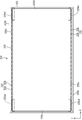
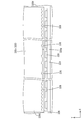
- FIG. 1 is an exploded perspective view of a television receiver TV according to Embodiment 1.
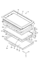
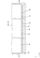
- FIG. Disassembled perspective view of liquid crystal display device An enlarged cross-sectional view in which the vicinity of the LED in the cross section obtained by cutting the liquid crystal display device along the short side direction of the chassis is enlarged.
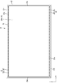
- a plan view of the backlight device viewed from the front side
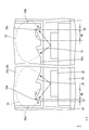
- the enlarged plan view in which the vicinity of the LED is enlarged in FIG. A plan view schematically showing a path of light incident on a light incident surface
- the top view which looked at the backlight apparatus from the front side in Embodiment 3 The enlarged plan view which expanded LED vicinity in Embodiment 3.
- Embodiment 1 will be described with reference to the drawings.
- the television receiver TV is illustrated.
- a part of each drawing shows an X-axis, a Y-axis, and a Z-axis, and each axis direction is drawn in a common direction in each drawing.
- the Y-axis direction coincides with the vertical direction
- the X-axis direction coincides with the horizontal direction.
- the vertical direction is used as a reference for upper and lower descriptions.
- the television receiver TV includes a liquid crystal display device (an example of a display device) 10, front and back cabinets Ca and Cb that are accommodated so as to sandwich the liquid crystal display device 10, a power source P, a tuner T, and a stand S. ing.
- the liquid crystal display device 10 has a horizontally long rectangular shape as a whole, and includes a liquid crystal panel 16 that is a display panel and a backlight device (an example of an illumination device) 24 that is an external light source, and these form a frame shape.
- the bezel 12 and the like are integrally held.
- the liquid crystal panel 16 is assembled in a posture in which a display surface capable of displaying an image faces the front side.
- the liquid crystal panel 16 has a configuration in which a pair of transparent (highly translucent) glass substrates are bonded together with a predetermined gap therebetween, and a liquid crystal layer (not shown) is sealed between the glass substrates. Is done.
- One glass substrate is provided with a switching element (for example, TFT) connected to a source wiring and a gate wiring orthogonal to each other, a pixel electrode connected to the switching element, an alignment film, and the like.
- the substrate is provided with a color filter and counter electrodes in which colored portions such as R (red), G (green), and B (blue) are arranged in a predetermined arrangement, and an alignment film.
- image data and various control signals necessary for displaying an image are supplied to a source wiring, a gate wiring, a counter electrode, and the like from a drive circuit board (not shown).
- a polarizing plate (not shown) is disposed outside both glass substrates.
- the backlight device 24 includes a substantially box-shaped chassis 22 that opens toward the front side (light emission side, liquid crystal panel 16 side), a frame 14 disposed on the front side of the chassis 22, And an optical member 18 disposed so as to cover the opening of the frame 14. Further, a pair of LED (Light Emitting Diode) units 32 and 32, four spacers 34, a reflection sheet 26, and a light guide plate 20 are accommodated in the chassis 22. Both side surfaces (light incident surfaces) 20a on the long side of the light guide plate 20 are disposed at positions facing the LED units 32, and guide light emitted from the LED units 32 to the liquid crystal panel 16 side.
- LED Light Emitting Diode
- the optical member 18 is placed on the front side of the light guide plate 20.
- the light guide plate 20 and the optical member 18 are disposed directly below the liquid crystal panel 16 and the LED unit 32 that is a light source is disposed on the side end of the light guide plate 20.
- a so-called edge light system (side light system) is adopted. Below, each component of the backlight apparatus 24 is demonstrated in detail.
- the chassis 22 is made of, for example, a metal plate such as an aluminum plate or an electrogalvanized steel plate (SECC). As shown in FIG. 2, the chassis 22 has a horizontally long bottom plate 22a and both the bottom plate 22a. The side plate 22b rises from each outer edge of the side, and the side plate rises from each outer edge of both short sides of the bottom plate 22a. A space sandwiched between the pair of LED units 32 and 32 in the chassis 22 is a housing space for the light guide plate 20 described later.
- the chassis 22 (bottom plate 22a) has a long side direction that matches the X-axis direction (horizontal direction), and a short side direction that matches the Y-axis direction (vertical direction).
- a projecting portion 22a1 having a frame shape in a plan view projecting toward the light guide plate 20 is provided at an edge portion of the surface of the bottom plate 22a.
- the top surface of the protruding portion 22 is a flat surface, and the light guide plate 20 can be placed along the edge of the spacer 34 via the spacer 34.
- the protruding portion 22a1 supports the light guide plate 20 and the reflection sheet 26 accommodated in the chassis 22 from the back side.
- a control board (not shown) for supplying a driving signal to the liquid crystal panel 16 is attached to the outside of the back side of the bottom plate 22a. Note that other substrates such as an LED driving substrate (not shown) for supplying driving power to the LED unit 32 are attached to the bottom plate 22a in the same manner as the control substrate described above.
- the frame 14 is made of synthetic resin such as plastic, and as shown in FIGS. 2 and 3, the frame 14 is parallel to the optical member 18 and the light guide plate 20 (liquid crystal panel 16) and has a substantially frame shape when viewed in plan. It is comprised from a site
- the substantially frame-shaped portion of the frame 14 extends along the outer peripheral edge portion of the light guide plate 20, and the optical member 18 and the outer peripheral edge portion of the light guide plate 20 arranged on the back side of the frame 14 face the entire surface. It is possible to cover from.
- the substantially frame-shaped portion of the frame 14 can receive (support) the outer peripheral end of the optical member 18 disposed on the front side from the back side over substantially the entire circumference.
- the substantially frame-shaped portion of the frame 14 is disposed so as to be interposed between the optical member 18 and the light guide plate 20.
- one long side portion covers the end portion on the light incident surface 20 a side of the light guide plate 20 and the LED unit 32 collectively from the front side.
- a portion having a substantially short cylindrical shape in the frame 14 is attached in a state of being directed to the outer surface of the side plate 22 b of the chassis 22. The outer surface of the part is arranged in contact with the inner surface of the cylindrical plate surface of the bezel 12 described above.
- the optical member 18 is formed by laminating a diffusion sheet 18a, a lens sheet 18b, and a reflective polarizing plate 18c in order from the light guide plate 20 side.
- the diffusion sheet 18a, the lens sheet 18b, and the reflective polarizing plate 18c have a function of converting light emitted from the LED unit 32 and passing through the light guide plate 20 into planar light.
- the liquid crystal panel 16 is installed on the upper surface side of the reflective polarizing plate 18d, and the optical member 18 is stably disposed in a form sandwiched between the frame 14 and the liquid crystal panel 16. That is, the optical member 18 is slightly larger than the inner edge of the frame 14 and is placed on the surface of the inner edge. Therefore, as shown in the sectional view of FIG. 3, the space formed between the LED 28 and the light guide plate 20 and the end of the optical member 18 are separated by the frame 14.
- the reflection sheet 26 has a rectangular sheet shape, is made of a synthetic resin, and has a white surface with excellent light reflectivity.
- the reflection sheet 26 has a shape in which the long side direction coincides with the X-axis direction, the short side direction coincides with the Y-axis direction, and is sandwiched between the opposite surface 20c of the light guide plate 20 and a spacer 34 described later. (See FIG. 3).
- the reflection sheet 26 has a reflection surface on the front side, and this reflection surface is in contact with the opposite surface 20 c of the light guide plate 20. And the reflection sheet 26 can reflect the light which leaked from the LED unit 32 or the light-guide plate 20 to the reflective surface side.
- the reflection sheet 26 is slightly larger than the opposite surface 20c of the light guide plate 20, and its end edge slightly protrudes from the end portion of the light guide plate 20 as shown in FIGS. ing.
- the four spacers 34 are arranged along the short side direction and the long side direction of the chassis 22 respectively, and have a flat plate shape. Each spacer 34 is placed on the top surface of the protruding portion 22 a 1 of the chassis 22. As described above, the edge of the reflection sheet 26 is sandwiched between the spacers 34 and the light guide plate 20. By sandwiching the reflection sheet in this way, the reflection sheet 26 is fixed, and movement in the plate surface direction of the light guide plate 20 (the plate surface direction of the bottom plate 22a of the chassis 22 and the XY plane direction) is restricted. It has a configuration.
- the pair of LED units 32, 32 are arranged on both long sides of the chassis 22, and are composed of an LED substrate 30 and an LED 28.
- the LED substrate 30 constituting the LED unit 32 is an elongated plate extending along the long side direction of the light guide plate 20 (X-axis direction, long side direction of the light incident surface 20a).
- the plate surface is accommodated in the chassis 22 in a posture parallel to the X-axis direction and the Z-axis direction, that is, a posture parallel to the light incident surface 20a of the light guide plate 20.
- Each LED substrate 30 has a size in the long side direction (X-axis direction) that is approximately the same as the size in the long side direction of the light guide plate 20.
- a plurality of LEDs 28 described below are surface-mounted on the inner side of the LED substrate 30, that is, the plate surface facing the light guide plate 20 side (the surface facing the light guide plate 20).
- the surface 30a On the mounting surface 30a of the LED substrate 30, a wiring pattern (not shown) made of a metal film (such as copper foil) that extends along the X-axis direction and connects the adjacent LEDs 28 across the LED 28 group in series.
- the terminal portions formed at both ends of the wiring pattern are connected to the power supply board via wiring members such as connectors and electric wires so that driving power is supplied to each LED 28. It has become.
- the plate surface opposite to the mounting surface 30 a of the LED substrate 30 is attached to the side plate 22 b on the long side of the chassis 22 by screwing or the like.
- the LED 28 constituting the LED unit 32 is configured such that an LED element (not shown) is sealed with a resin material on a substrate portion fixed to the LED substrate 30.
- the LED element mounted on the substrate portion has one main emission wavelength, and specifically, one that emits blue light in a single color is used.
- a phosphor that emits a predetermined color by being excited by blue light emitted from the LED element is dispersed and mixed, and generally emits white light as a whole. It is said.
- a yellow phosphor that emits yellow light for example, a green phosphor that emits green light, and a red phosphor that emits red light are used in appropriate combination, or any one of them is used. It can be used alone.
- the LED 28 is a so-called top surface light emitting type in which a surface opposite to the mounting surface 30a with respect to the LED substrate 30 (a surface facing the light incident surface 20a of the light guide plate 20) is a main light emitting surface.
- the light guide plate 20 is made of a synthetic resin material (for example, acrylic resin such as PMMA or polycarbonate) having a refractive index sufficiently higher than that of air and almost transparent (excellent translucency).
- the light guide plate 20 has a horizontally long rectangular shape when viewed in plan as in the case of the liquid crystal panel 16 and the chassis 22, and has a plate shape that is thicker than the optical member 18.
- the long side direction in FIG. 4 coincides with the X-axis direction
- the short side direction coincides with the Y-axis direction
- the plate thickness direction perpendicular to the plate surface coincides with the Z-axis direction.
- Both end surfaces on the long side of the light guide plate 20 are light incident surfaces 20a on which light emitted from the LEDs 28 is incident.
- the light incident surface 20a is provided with irregularities 36 to be described later.
- both end surfaces on the short side of the light guide plate 20, that is, both end surfaces adjacent to the light incident surface 20a are adjacent end surfaces 20d.
- the light guide plate 20 has a light incident surface 20a facing the LED unit 32, and a light emitting surface 20b that is a main plate surface (front plate surface) on the optical member 18 side.
- the opposite surface 20c which is the plate surface opposite to the light emitting surface 20b (the plate surface on the back side), is arranged so as to face the reflection sheet 26 side, and a later-described protruding portion of the chassis 22 through the reflection sheet 26 22a1 is supported.
- the alignment direction with the LED unit 32 coincides with the Y-axis direction
- the alignment direction with the optical member 18 and the reflection sheet 26 coincides with the Z-axis direction.
- the light guide plate 20 introduces light emitted from the LED unit 32 along the Y-axis direction from the light incident surface 20a, rises toward the optical member 18 side while propagating the light inside, and emits light. It has the function to emit from 20b.
- the light incident surface 20a of the light guide plate 20 is provided with a plurality of irregularities 36 over the entire surface.
- These irregularities 36 have a prism shape formed such that light emitted from each LED 28 and incident from the light incident surface 20 a is relatively directed to the adjacent end surface 20 d side rather than the center side of the light guide plate 20.
- each of the irregularities 36 extends in a direction orthogonal to the plate surface of the light guide plate 20 (Z-axis direction), and in the center of the light guide plate 20 in a plan view of the light guide plate 20. It is a prism lens that is recessed in a triangular shape.
- the triangular apex portion 36a (see FIG. 6) of the prism lens is formed to be relatively unevenly distributed closer to the adjacent end face 20d.
- the prism lens that forms each of the irregularities 36 has a shape in which the triangular apex portion 36a is unevenly distributed, and as shown in FIG. 6, the two sides that constitute the apex portion 36a.
- the lengths L1 and L4 of the sides relatively positioned on the adjacent end surface 20d side are relatively shorter than the lengths L2 and L3 of the sides positioned on the center side of the light incident surface 20a.
- corrugation 36 provided in the light-incidence surface 20a is made into the above shapes, the light radiate
- the light guide plate 20 spreads toward the adjacent end face 20d side relative to the center side of the light guide plate 20. Thereby, it can suppress that the light from each LED28 overlaps more in the site
- the in-plane luminance distribution on the light emitting surface 20b can be controlled to be substantially uniform in a plan view of the light guide plate 20.
- the light incident from the light incident surface 20a of the light guide plate 20 is directed to the adjacent end surface 20d side by the unevenness 36.
- the lens member or the like is not disposed in the middle of the light path as in the configuration described in the prior art, it is possible to prevent the light utilization efficiency from being lowered.
- the uniformity of the luminance distribution on the light exit surface 20b is improved without reducing the light use efficiency. Can be made.
- each of the irregularities 36 extends in a direction orthogonal to the plate surface of the light guide plate 20 (Z-axis direction) and has a triangular shape toward the center of the light guide plate 20 in a plan view of the light guide plate 20. It is a hollow prism lens, and the triangular apex portion 26a is relatively unevenly distributed closer to the adjacent end face 20d side.
- each of the projections and depressions 36 is relatively light-incident on the side located on the side of the adjacent end face 20d relative to the two sides constituting the triangular apex portion 26a in plan view of the light guide plate 20. The length is shorter than the side located on the center side of the surface 20a.
- corrugation 36 in which the light which injected from the light-incidence surface 20a goes to the adjacent end surface 20d side relatively rather than the center side of the light-guide plate 20 is implement
- the unevenness 36 is provided over the entire surface of the light incident surface 20a. With such a configuration, all the light incident from the light incident surface 20a can be directed to the adjacent end surface 20d side by the unevenness 36, so that the uniformity of the luminance distribution on the light emitting surface 20b is effective. Can be improved.
- the light guide plate 20 is made of synthetic resin. Therefore, when the light guide plate 20 is processed in the manufacturing process, the unevenness 36 can be easily formed on the light incident surface 20a by injection molding or the like.
- the plurality of LEDs 28 are linearly arranged at substantially equal intervals along the light incident surface 20a.
- the LEDs 28 are regularly arranged on the LED substrate 30 and the like, so that compared with the case where the LEDs 28 are irregularly arranged.
- the LED 28 can be easily arranged, and workability in the manufacturing process of the backlight device 24 can be improved.
- each of the irregularities 136 is a prism lens that extends in a direction (Z-axis direction) orthogonal to the plate surface of the light guide plate 120 and projects in a triangular shape toward the outside of the light guide plate 120 in a plan view of the light guide plate 120.
- the apex portion of the triangular shape is relatively unevenly distributed closer to the adjacent end face 120d side.
- Embodiment 3 will be described with reference to the drawings.
- the third embodiment is different from that of the first embodiment in that the unevenness 236 is provided only on a part of the light incident surface 220 a of the light guide plate 220. Since the other configuration is the same as that of the first embodiment, the description of the structure, operation, and effect is omitted.
- FIGS. 8 and 9 the portions obtained by adding the numeral 200 to the reference numerals in FIGS. 4 and 5 are the same as the portions described in the first embodiment.
- the unevenness 236 is provided only in the portion 220 a 1 closer to the adjacent end surface 220 d side of the light incident surface 220 a of the light guide plate 220.
- the shape of the unevenness 236 is the same as that described in the first embodiment.
- the unevenness 236 is provided on the light incident surface 220a in the arrangement as described above, the light incident on the portion of the light incident surface where the unevenness 236 is not provided is on both adjacent end surfaces 220d side. While the light spreads uniformly, the light incident on the portion where the unevenness 236 is provided is directed toward the adjacent end face 220d.
- the unevenness 236 is arranged as in this embodiment, even when the interval between the adjacent LEDs 228 is narrowed, for example, more light overlaps at the center side than at both end sides of the light incident surface 220a. It is possible to prevent the luminance from becoming uneven between the center side and both end sides of the light emitting surface 220b.
- the unevenness 236 is provided only in a portion of the light incident surface 220a that is relatively closer to the adjacent end surface 220d side, so that the unevenness 236 is formed on the entire surface of the light incident surface 220a.
- the processing cost of the light guide plate 220 can be reduced.
- Embodiment 4 will be described with reference to the drawings.
- the density of the unevenness 336 provided on the light incident surface 320a of the light guide plate 320 is different from that of the first embodiment. Since the other configuration is the same as that of the first embodiment, the description of the structure, operation, and effect is omitted.
- FIG. 10 the part obtained by adding the numeral 300 to the reference numeral in FIG. 5 is the same as the part described in the first embodiment.
- the unevenness 336 provided relatively closer to the adjacent end surface 320 d side of the light incident surface 320 a is relatively provided closer to the center side. It is more densely provided. With this configuration, in the present embodiment, more light incident from the adjacent end surface 320d side than the central side of the light incident surface 320a can be directed toward the adjacent end surface 320d. it can. For this reason, the uniformity of the luminance distribution on the light emitting surface 320b can be more effectively improved.
- the television receiver provided with a tuner is exemplified, but the present invention can also be applied to a display device not provided with a tuner.
- TV TV receiver, Ca, Cb: cabinet, T: tuner, S: stand
- 10 liquid crystal display
- 12 bezel
- 14 frame
- 16 liquid crystal panel
- 18 optical member
- 20, 120, 220, 320 Light guide plate, 20a, 120a, 220a, 320a: Light incident surface
- 20b, 120b, 220b, 320b Light exit surface
- 22 Chassis
- 24 Backlight device
- 36a apex angle portion
Landscapes
- Physics & Mathematics (AREA)
- Nonlinear Science (AREA)
- General Physics & Mathematics (AREA)
- Optics & Photonics (AREA)
- Engineering & Computer Science (AREA)
- Multimedia (AREA)
- Signal Processing (AREA)
- Mathematical Physics (AREA)
- Chemical & Material Sciences (AREA)
- Crystallography & Structural Chemistry (AREA)
- Planar Illumination Modules (AREA)
Abstract
Selon l'invention, un dispositif de rétroéclairage est équipé : d'une pluralité de DEL (28) disposée en rangs ; et d'une plaque de guidage de lumière (20) dans laquelle deux faces extrémité côté longueur servent de faces d'incidence de lumière (20a) sur laquelle une lumière provenant de la pluralité de DEL (28) est incidente, et des faces extrémité adjacentes des faces d'incidence de lumière (20a) servent de faces extrémité contiguës (20d), et dans laquelle une pluralité de creux et reliefs (36) sous forme de prismes formés de sorte qu'une lumière incidente par la face d'incidence de lumière (20a) est orientée de manière relative côté face extrémité contiguës (20d) par rapport au côté centre de la plaque de guidage de lumière (20), est agencée sur la face d'incidence de lumière (20a). Dans le dispositif de rétroéclairage (24), afin d'orienter la lumière incidente par les faces d'incidence de lumière (20a) de la plaque de guidage de lumière (20), côté faces extrémité contiguës (20d) à l'aide des creux et reliefs (36), il est possible de supprimer la superposition de lumières plus nombreuses côté centre que des deux côtés extrémité des faces d'incidence de lumière (20a) , et il est également possible de prévenir ou de supprimer un manque d'uniformité de luminance entre le côté centre et les deux côtés extrémité des faces émission en sortie de lumière (20b).
Priority Applications (1)
| Application Number | Priority Date | Filing Date | Title |
|---|---|---|---|
| US14/896,312 US20160124270A1 (en) | 2013-06-07 | 2014-02-28 | Illumination device, display device, and tv receiver |
Applications Claiming Priority (2)
| Application Number | Priority Date | Filing Date | Title |
|---|---|---|---|
| JP2013-120763 | 2013-06-07 | ||
| JP2013120763 | 2013-06-07 |
Publications (1)
| Publication Number | Publication Date |
|---|---|
| WO2014196235A1 true WO2014196235A1 (fr) | 2014-12-11 |
Family
ID=52007891
Family Applications (1)
| Application Number | Title | Priority Date | Filing Date |
|---|---|---|---|
| PCT/JP2014/055025 Ceased WO2014196235A1 (fr) | 2013-06-07 | 2014-02-28 | Dispositif d'éclairage, dispositif d'affichage et dispositif de réception de télévision |
Country Status (2)
| Country | Link |
|---|---|
| US (1) | US20160124270A1 (fr) |
| WO (1) | WO2014196235A1 (fr) |
Families Citing this family (5)
| Publication number | Priority date | Publication date | Assignee | Title |
|---|---|---|---|---|
| JP2018522367A (ja) * | 2015-05-13 | 2018-08-09 | コーニング インコーポレイテッド | ホットスポットを減少した導光体およびその製造方法 |
| CN105868742B (zh) * | 2016-05-26 | 2020-07-03 | 京东方科技集团股份有限公司 | 显示组件和显示装置 |
| CN107884869A (zh) * | 2017-11-28 | 2018-04-06 | 合肥泰沃达智能装备有限公司 | 一种防漏光导光板的背光模组 |
| DE102018216342A1 (de) * | 2018-09-25 | 2020-03-26 | Continental Automotive Gmbh | Anzeige aufweisend ein LCD mit Hintergrundbeleuchtung |
| JP7373293B2 (ja) * | 2019-04-12 | 2023-11-02 | 株式会社ジャパンディスプレイ | 光源装置 |
Citations (3)
| Publication number | Priority date | Publication date | Assignee | Title |
|---|---|---|---|---|
| JP2000299011A (ja) * | 1999-04-13 | 2000-10-24 | Nippon Denyo | 平面照明装置 |
| JP2006114503A (ja) * | 2004-10-14 | 2006-04-27 | Kofukin Seimitsu Kogyo (Shenzhen) Yugenkoshi | 導光板及びバックライトモジュール |
| JP2008047429A (ja) * | 2006-08-17 | 2008-02-28 | Epson Imaging Devices Corp | 照明装置、液晶装置及び電子機器 |
Family Cites Families (2)
| Publication number | Priority date | Publication date | Assignee | Title |
|---|---|---|---|---|
| CN100434988C (zh) * | 2004-02-16 | 2008-11-19 | 西铁城电子股份有限公司 | 导光板 |
| CN100412573C (zh) * | 2005-04-15 | 2008-08-20 | 鸿富锦精密工业(深圳)有限公司 | 双面导光板、面光源装置及显示装置 |
-
2014
- 2014-02-28 WO PCT/JP2014/055025 patent/WO2014196235A1/fr not_active Ceased
- 2014-02-28 US US14/896,312 patent/US20160124270A1/en not_active Abandoned
Patent Citations (3)
| Publication number | Priority date | Publication date | Assignee | Title |
|---|---|---|---|---|
| JP2000299011A (ja) * | 1999-04-13 | 2000-10-24 | Nippon Denyo | 平面照明装置 |
| JP2006114503A (ja) * | 2004-10-14 | 2006-04-27 | Kofukin Seimitsu Kogyo (Shenzhen) Yugenkoshi | 導光板及びバックライトモジュール |
| JP2008047429A (ja) * | 2006-08-17 | 2008-02-28 | Epson Imaging Devices Corp | 照明装置、液晶装置及び電子機器 |
Also Published As
| Publication number | Publication date |
|---|---|
| US20160124270A1 (en) | 2016-05-05 |
Similar Documents
| Publication | Publication Date | Title |
|---|---|---|
| US9632237B2 (en) | Illumination device, display device, and TV receiver | |
| US10434746B2 (en) | Laminated optical member, lighting device, display device, and television device with spacers defined in linear shapes along a plate surface with axes tilted relative to an arrangement direction of pixels | |
| US8579454B2 (en) | Lighting device, display device and television device | |
| WO2013051473A1 (fr) | Dispositif d'éclairage, dispositif d'affichage et appareil de réception de télévision | |
| WO2011077866A1 (fr) | Dispositif d'éclairage, dispositif d'affichage et dispositif de récepteur de télévision | |
| CN102239360A (zh) | 照明装置、显示装置和电视接收装置 | |
| WO2013039001A1 (fr) | Dispositif d'éclairage, dispositif d'affichage et dispositif de réception de télévision | |
| KR102090457B1 (ko) | 액정표시장치 | |
| WO2011058960A1 (fr) | Dispositif d'éclairage, dispositif d'affichage et récepteur de télévision | |
| WO2011111444A1 (fr) | Dispositif d'éclairage, appareil d'affichage et récepteur de télévision | |
| CN110632698A (zh) | 照明装置和显示装置 | |
| WO2014196235A1 (fr) | Dispositif d'éclairage, dispositif d'affichage et dispositif de réception de télévision | |
| WO2016181838A1 (fr) | Dispositif d'éclairage, dispositif d'affichage, et récepteur de télévision | |
| CN104412030A (zh) | 显示装置和电视接收装置 | |
| CN105190154B (zh) | 照明装置、显示装置以及电视接收装置 | |
| KR101995777B1 (ko) | 백라이트 유닛 및 이를 포함하는 액정표시장치 | |
| WO2011092953A1 (fr) | Dispositif d'éclairage, écran et dispositif de téléviseur | |
| WO2013047367A1 (fr) | Dispositif d'affichage et dispositif de réception de télévision | |
| WO2011111445A1 (fr) | Dispositif d'éclairage, appareil d'affichage et récepteur de télévision | |
| WO2014196234A1 (fr) | Dispositif d'éclairage, dispositif d'affichage et dispositif de réception de télévision | |
| US8976304B2 (en) | Display device and television receiver device | |
| JP2013149559A (ja) | 照明装置、表示装置、及びテレビ受信装置 | |
| WO2012111501A1 (fr) | Dispositif d'éclairage, dispositif d'affichage et dispositif récepteur de télévision | |
| KR20160059006A (ko) | 백라이트 유닛 및 이를 구비한 액정표시장치 | |
| WO2012169440A1 (fr) | Dispositif d'éclairage, dispositif d'affichage, et dispositif de réception de télévision |
Legal Events
| Date | Code | Title | Description |
|---|---|---|---|
| 121 | Ep: the epo has been informed by wipo that ep was designated in this application |
Ref document number: 14808074 Country of ref document: EP Kind code of ref document: A1 |
|
| WWE | Wipo information: entry into national phase |
Ref document number: 14896312 Country of ref document: US |
|
| NENP | Non-entry into the national phase |
Ref country code: DE |
|
| 122 | Ep: pct application non-entry in european phase |
Ref document number: 14808074 Country of ref document: EP Kind code of ref document: A1 |
|
| NENP | Non-entry into the national phase |
Ref country code: JP |