WO2014199975A1 - Matériau de fenêtre pour élément d'émission de rayons ultraviolets et procédé de production associé - Google Patents
Matériau de fenêtre pour élément d'émission de rayons ultraviolets et procédé de production associé Download PDFInfo
- Publication number
- WO2014199975A1 WO2014199975A1 PCT/JP2014/065317 JP2014065317W WO2014199975A1 WO 2014199975 A1 WO2014199975 A1 WO 2014199975A1 JP 2014065317 W JP2014065317 W JP 2014065317W WO 2014199975 A1 WO2014199975 A1 WO 2014199975A1
- Authority
- WO
- WIPO (PCT)
- Prior art keywords
- ultraviolet light
- window material
- light emitting
- emitting element
- substrate
- Prior art date
- Legal status (The legal status is an assumption and is not a legal conclusion. Google has not performed a legal analysis and makes no representation as to the accuracy of the status listed.)
- Ceased
Links
Images


Classifications
-
- C—CHEMISTRY; METALLURGY
- C04—CEMENTS; CONCRETE; ARTIFICIAL STONE; CERAMICS; REFRACTORIES
- C04B—LIME, MAGNESIA; SLAG; CEMENTS; COMPOSITIONS THEREOF, e.g. MORTARS, CONCRETE OR LIKE BUILDING MATERIALS; ARTIFICIAL STONE; CERAMICS; REFRACTORIES; TREATMENT OF NATURAL STONE
- C04B35/00—Shaped ceramic products characterised by their composition; Ceramics compositions; Processing powders of inorganic compounds preparatory to the manufacturing of ceramic products
- C04B35/01—Shaped ceramic products characterised by their composition; Ceramics compositions; Processing powders of inorganic compounds preparatory to the manufacturing of ceramic products based on oxide ceramics
- C04B35/10—Shaped ceramic products characterised by their composition; Ceramics compositions; Processing powders of inorganic compounds preparatory to the manufacturing of ceramic products based on oxide ceramics based on aluminium oxide
- C04B35/111—Fine ceramics
- C04B35/115—Translucent or transparent products
-
- B—PERFORMING OPERATIONS; TRANSPORTING
- B29—WORKING OF PLASTICS; WORKING OF SUBSTANCES IN A PLASTIC STATE IN GENERAL
- B29B—PREPARATION OR PRETREATMENT OF THE MATERIAL TO BE SHAPED; MAKING GRANULES OR PREFORMS; RECOVERY OF PLASTICS OR OTHER CONSTITUENTS OF WASTE MATERIAL CONTAINING PLASTICS
- B29B11/00—Making preforms
- B29B11/14—Making preforms characterised by structure or composition
-
- B—PERFORMING OPERATIONS; TRANSPORTING
- B29—WORKING OF PLASTICS; WORKING OF SUBSTANCES IN A PLASTIC STATE IN GENERAL
- B29C—SHAPING OR JOINING OF PLASTICS; SHAPING OF MATERIAL IN A PLASTIC STATE, NOT OTHERWISE PROVIDED FOR; AFTER-TREATMENT OF THE SHAPED PRODUCTS, e.g. REPAIRING
- B29C49/00—Blow-moulding, i.e. blowing a preform or parison to a desired shape within a mould; Apparatus therefor
- B29C49/071—Preforms or parisons characterised by their configuration, e.g. geometry, dimensions or physical properties
-
- C—CHEMISTRY; METALLURGY
- C04—CEMENTS; CONCRETE; ARTIFICIAL STONE; CERAMICS; REFRACTORIES
- C04B—LIME, MAGNESIA; SLAG; CEMENTS; COMPOSITIONS THEREOF, e.g. MORTARS, CONCRETE OR LIKE BUILDING MATERIALS; ARTIFICIAL STONE; CERAMICS; REFRACTORIES; TREATMENT OF NATURAL STONE
- C04B35/00—Shaped ceramic products characterised by their composition; Ceramics compositions; Processing powders of inorganic compounds preparatory to the manufacturing of ceramic products
- C04B35/622—Forming processes; Processing powders of inorganic compounds preparatory to the manufacturing of ceramic products
- C04B35/626—Preparing or treating the powders individually or as batches ; preparing or treating macroscopic reinforcing agents for ceramic products, e.g. fibres; mechanical aspects section B
- C04B35/62605—Treating the starting powders individually or as mixtures
- C04B35/62645—Thermal treatment of powders or mixtures thereof other than sintering
- C04B35/62655—Drying, e.g. freeze-drying, spray-drying, microwave or supercritical drying
-
- C—CHEMISTRY; METALLURGY
- C04—CEMENTS; CONCRETE; ARTIFICIAL STONE; CERAMICS; REFRACTORIES
- C04B—LIME, MAGNESIA; SLAG; CEMENTS; COMPOSITIONS THEREOF, e.g. MORTARS, CONCRETE OR LIKE BUILDING MATERIALS; ARTIFICIAL STONE; CERAMICS; REFRACTORIES; TREATMENT OF NATURAL STONE
- C04B35/00—Shaped ceramic products characterised by their composition; Ceramics compositions; Processing powders of inorganic compounds preparatory to the manufacturing of ceramic products
- C04B35/622—Forming processes; Processing powders of inorganic compounds preparatory to the manufacturing of ceramic products
- C04B35/626—Preparing or treating the powders individually or as batches ; preparing or treating macroscopic reinforcing agents for ceramic products, e.g. fibres; mechanical aspects section B
- C04B35/63—Preparing or treating the powders individually or as batches ; preparing or treating macroscopic reinforcing agents for ceramic products, e.g. fibres; mechanical aspects section B using additives specially adapted for forming the products, e.g.. binder binders
- C04B35/632—Organic additives
- C04B35/634—Polymers
-
- C—CHEMISTRY; METALLURGY
- C04—CEMENTS; CONCRETE; ARTIFICIAL STONE; CERAMICS; REFRACTORIES
- C04B—LIME, MAGNESIA; SLAG; CEMENTS; COMPOSITIONS THEREOF, e.g. MORTARS, CONCRETE OR LIKE BUILDING MATERIALS; ARTIFICIAL STONE; CERAMICS; REFRACTORIES; TREATMENT OF NATURAL STONE
- C04B35/00—Shaped ceramic products characterised by their composition; Ceramics compositions; Processing powders of inorganic compounds preparatory to the manufacturing of ceramic products
- C04B35/622—Forming processes; Processing powders of inorganic compounds preparatory to the manufacturing of ceramic products
- C04B35/626—Preparing or treating the powders individually or as batches ; preparing or treating macroscopic reinforcing agents for ceramic products, e.g. fibres; mechanical aspects section B
- C04B35/63—Preparing or treating the powders individually or as batches ; preparing or treating macroscopic reinforcing agents for ceramic products, e.g. fibres; mechanical aspects section B using additives specially adapted for forming the products, e.g.. binder binders
- C04B35/638—Removal thereof
-
- G—PHYSICS
- G02—OPTICS
- G02B—OPTICAL ELEMENTS, SYSTEMS OR APPARATUS
- G02B1/00—Optical elements characterised by the material of which they are made; Optical coatings for optical elements
- G02B1/10—Optical coatings produced by application to, or surface treatment of, optical elements
- G02B1/12—Optical coatings produced by application to, or surface treatment of, optical elements by surface treatment, e.g. by irradiation
-
- G—PHYSICS
- G02—OPTICS
- G02B—OPTICAL ELEMENTS, SYSTEMS OR APPARATUS
- G02B5/00—Optical elements other than lenses
- G02B5/02—Diffusing elements; Afocal elements
- G02B5/0205—Diffusing elements; Afocal elements characterised by the diffusing properties
- G02B5/0236—Diffusing elements; Afocal elements characterised by the diffusing properties the diffusion taking place within the volume of the element
- G02B5/0242—Diffusing elements; Afocal elements characterised by the diffusing properties the diffusion taking place within the volume of the element by means of dispersed particles
-
- G—PHYSICS
- G02—OPTICS
- G02B—OPTICAL ELEMENTS, SYSTEMS OR APPARATUS
- G02B5/00—Optical elements other than lenses
- G02B5/02—Diffusing elements; Afocal elements
- G02B5/0273—Diffusing elements; Afocal elements characterized by the use
- G02B5/0278—Diffusing elements; Afocal elements characterized by the use used in transmission
-
- B—PERFORMING OPERATIONS; TRANSPORTING
- B29—WORKING OF PLASTICS; WORKING OF SUBSTANCES IN A PLASTIC STATE IN GENERAL
- B29C—SHAPING OR JOINING OF PLASTICS; SHAPING OF MATERIAL IN A PLASTIC STATE, NOT OTHERWISE PROVIDED FOR; AFTER-TREATMENT OF THE SHAPED PRODUCTS, e.g. REPAIRING
- B29C2949/00—Indexing scheme relating to blow-moulding
- B29C2949/07—Preforms or parisons characterised by their configuration
- B29C2949/0715—Preforms or parisons characterised by their configuration the preform having one end closed
-
- B—PERFORMING OPERATIONS; TRANSPORTING
- B29—WORKING OF PLASTICS; WORKING OF SUBSTANCES IN A PLASTIC STATE IN GENERAL
- B29K—INDEXING SCHEME ASSOCIATED WITH SUBCLASSES B29B, B29C OR B29D, RELATING TO MOULDING MATERIALS OR TO MATERIALS FOR MOULDS, REINFORCEMENTS, FILLERS OR PREFORMED PARTS, e.g. INSERTS
- B29K2505/00—Use of metals, their alloys or their compounds, as filler
- B29K2505/02—Aluminium
-
- B—PERFORMING OPERATIONS; TRANSPORTING
- B29—WORKING OF PLASTICS; WORKING OF SUBSTANCES IN A PLASTIC STATE IN GENERAL
- B29L—INDEXING SCHEME ASSOCIATED WITH SUBCLASS B29C, RELATING TO PARTICULAR ARTICLES
- B29L2011/00—Optical elements, e.g. lenses, prisms
-
- C—CHEMISTRY; METALLURGY
- C04—CEMENTS; CONCRETE; ARTIFICIAL STONE; CERAMICS; REFRACTORIES
- C04B—LIME, MAGNESIA; SLAG; CEMENTS; COMPOSITIONS THEREOF, e.g. MORTARS, CONCRETE OR LIKE BUILDING MATERIALS; ARTIFICIAL STONE; CERAMICS; REFRACTORIES; TREATMENT OF NATURAL STONE
- C04B2235/00—Aspects relating to ceramic starting mixtures or sintered ceramic products
- C04B2235/02—Composition of constituents of the starting material or of secondary phases of the final product
- C04B2235/50—Constituents or additives of the starting mixture chosen for their shape or used because of their shape or their physical appearance
- C04B2235/54—Particle size related information
- C04B2235/5409—Particle size related information expressed by specific surface values
-
- C—CHEMISTRY; METALLURGY
- C04—CEMENTS; CONCRETE; ARTIFICIAL STONE; CERAMICS; REFRACTORIES
- C04B—LIME, MAGNESIA; SLAG; CEMENTS; COMPOSITIONS THEREOF, e.g. MORTARS, CONCRETE OR LIKE BUILDING MATERIALS; ARTIFICIAL STONE; CERAMICS; REFRACTORIES; TREATMENT OF NATURAL STONE
- C04B2235/00—Aspects relating to ceramic starting mixtures or sintered ceramic products
- C04B2235/60—Aspects relating to the preparation, properties or mechanical treatment of green bodies or pre-forms
- C04B2235/602—Making the green bodies or pre-forms by moulding
- C04B2235/6023—Gel casting
-
- C—CHEMISTRY; METALLURGY
- C04—CEMENTS; CONCRETE; ARTIFICIAL STONE; CERAMICS; REFRACTORIES
- C04B—LIME, MAGNESIA; SLAG; CEMENTS; COMPOSITIONS THEREOF, e.g. MORTARS, CONCRETE OR LIKE BUILDING MATERIALS; ARTIFICIAL STONE; CERAMICS; REFRACTORIES; TREATMENT OF NATURAL STONE
- C04B2235/00—Aspects relating to ceramic starting mixtures or sintered ceramic products
- C04B2235/60—Aspects relating to the preparation, properties or mechanical treatment of green bodies or pre-forms
- C04B2235/602—Making the green bodies or pre-forms by moulding
- C04B2235/6025—Tape casting, e.g. with a doctor blade
-
- C—CHEMISTRY; METALLURGY
- C04—CEMENTS; CONCRETE; ARTIFICIAL STONE; CERAMICS; REFRACTORIES
- C04B—LIME, MAGNESIA; SLAG; CEMENTS; COMPOSITIONS THEREOF, e.g. MORTARS, CONCRETE OR LIKE BUILDING MATERIALS; ARTIFICIAL STONE; CERAMICS; REFRACTORIES; TREATMENT OF NATURAL STONE
- C04B2235/00—Aspects relating to ceramic starting mixtures or sintered ceramic products
- C04B2235/70—Aspects relating to sintered or melt-casted ceramic products
- C04B2235/72—Products characterised by the absence or the low content of specific components, e.g. alkali metal free alumina ceramics
-
- C—CHEMISTRY; METALLURGY
- C04—CEMENTS; CONCRETE; ARTIFICIAL STONE; CERAMICS; REFRACTORIES
- C04B—LIME, MAGNESIA; SLAG; CEMENTS; COMPOSITIONS THEREOF, e.g. MORTARS, CONCRETE OR LIKE BUILDING MATERIALS; ARTIFICIAL STONE; CERAMICS; REFRACTORIES; TREATMENT OF NATURAL STONE
- C04B2235/00—Aspects relating to ceramic starting mixtures or sintered ceramic products
- C04B2235/70—Aspects relating to sintered or melt-casted ceramic products
- C04B2235/74—Physical characteristics
- C04B2235/78—Grain sizes and shapes, product microstructures, e.g. acicular grains, equiaxed grains, platelet-structures
- C04B2235/786—Micrometer sized grains, i.e. from 1 to 100 micron
-
- C—CHEMISTRY; METALLURGY
- C04—CEMENTS; CONCRETE; ARTIFICIAL STONE; CERAMICS; REFRACTORIES
- C04B—LIME, MAGNESIA; SLAG; CEMENTS; COMPOSITIONS THEREOF, e.g. MORTARS, CONCRETE OR LIKE BUILDING MATERIALS; ARTIFICIAL STONE; CERAMICS; REFRACTORIES; TREATMENT OF NATURAL STONE
- C04B2235/00—Aspects relating to ceramic starting mixtures or sintered ceramic products
- C04B2235/70—Aspects relating to sintered or melt-casted ceramic products
- C04B2235/95—Products characterised by their size, e.g. microceramics
-
- C—CHEMISTRY; METALLURGY
- C04—CEMENTS; CONCRETE; ARTIFICIAL STONE; CERAMICS; REFRACTORIES
- C04B—LIME, MAGNESIA; SLAG; CEMENTS; COMPOSITIONS THEREOF, e.g. MORTARS, CONCRETE OR LIKE BUILDING MATERIALS; ARTIFICIAL STONE; CERAMICS; REFRACTORIES; TREATMENT OF NATURAL STONE
- C04B2235/00—Aspects relating to ceramic starting mixtures or sintered ceramic products
- C04B2235/70—Aspects relating to sintered or melt-casted ceramic products
- C04B2235/96—Properties of ceramic products, e.g. mechanical properties such as strength, toughness, wear resistance
- C04B2235/963—Surface properties, e.g. surface roughness
Definitions
- the present invention relates to a window material for an ultraviolet light emitting element having good ultraviolet light transmittance from an ultraviolet light emitting element such as a light emitting diode, a laser diode, or a discharge lamp emitting an ultraviolet ray having a wavelength of 300 nm or less.
- an ultraviolet light emitting element such as a light emitting diode, a laser diode, or a discharge lamp emitting an ultraviolet ray having a wavelength of 300 nm or less.
- UV-C Ultraviolet light is used according to the length of its wavelength, and in particular, light in the wavelength range of 280 nm or less is called UV-C, and is used for sterilization and sterilization because it is highly bactericidal ( See JP 2008-091623 A).
- An ultraviolet light emitting element is mentioned as one of the light sources which emit an ultraviolet ray, and the ultraviolet light emitting element is covered with a translucent material as a window material for protection of the element.
- a glass material is used as a translucent material for the ultraviolet light emitting element, and high silica glass (quartz) or the like is used from the viewpoints of productivity, cost, and strength (see JP-A-2000-349348). ).
- quartz is used as a window material for an ultraviolet light emitting element, but quartz has a thermal conductivity as low as about 1 W / m ⁇ K. Therefore, the heat can not be dissipated efficiently, and there is a concern that the damage due to the temperature rise of the ultraviolet light emitting element and the deterioration are likely to occur.
- the forward total light transmittance decreases as the wavelength decreases. In particular, it is remarkable at 300 nm or less.
- the present invention has been made in consideration of such problems, and has a high thermal conductivity and can ensure a high transmittance to ultraviolet light of 300 nm or less, and is suitable for use in an ultraviolet light emitting element.
- An object of the present invention is to provide a window material for an ultraviolet light emitting element and a method of manufacturing the same.
- a window material for an ultraviolet light emitting device is a window material for an ultraviolet light emitting device disposed at least on the ultraviolet light emitting side of an ultraviolet light emitting device emitting ultraviolet light having a wavelength of 300 nm or less And has an average particle size of 6 to 60 ⁇ m on the surface.
- the substrate may have a plate shape having a thickness of 2.0 mm or less and have one surface and the other surface opposite to the one surface. .
- the thickness described above may be 1.5 mm or less, or 1.0 mm or less. Preferably it is 0.5 mm or less, More preferably, it is 0.3 mm or less.
- the other surface may be a surface on the ultraviolet incident side, and at least the other surface may have a surface roughness Ra of 0.2 ⁇ m or more. Preferably, it is 0.2 to 0.6 ⁇ m.
- the surface roughness of the one surface of the substrate is preferably different from the surface roughness of the other surface.
- the one surface is the surface on the ultraviolet light emission side
- the other surface is the surface on the ultraviolet light incidence side
- a method of manufacturing a window material for an ultraviolet light emitting element according to the second invention is a method of manufacturing a window material for an ultraviolet light emitting element for manufacturing a window material for an ultraviolet light emitting element according to the first invention described above
- the method is characterized in that it comprises a step of producing a substrate made of translucent alumina and having one surface and the other surface opposite to the one surface by a gel cast method or a tape forming method.
- the surface roughness of the one surface of the substrate may be made different from the surface roughness of the other surface.
- one surface or the other surface of the substrate may be mirror-polished, or one surface or the other surface of the substrate may be ground.
- the second invention may further include the step of mirror-polishing at least the one surface of the substrate to a surface roughness Ra of 0.03 ⁇ m or less.
- the surface roughness of at least the other surface of the substrate may be further increased.
- This treatment includes grinding at least the other surface of the substrate.
- baking of different types of setters may be brought into contact with one side and the other side of the molded body during baking of the molded body.
- the surface roughness of the other surface of the substrate may be increased by using, as a setter in contact with the other surface, a setter whose surface roughness is larger than that in contact with one surface.
- the method further comprises the step of mirror-polishing the one surface of the substrate to a surface roughness Ra of 0.03 ⁇ m or less, and further increasing the surface roughness of the other surface of the substrate Processing may be performed.
- This treatment includes grinding at least the other surface of the substrate.
- the window material for an ultraviolet light emitting element According to the window material for an ultraviolet light emitting element according to the present invention, high transmittance can be secured for ultraviolet light of 300 nm or less, and a window material suitable for the ultraviolet light emitting element can be obtained. Moreover, since the light-transmissive alumina substrate has a high thermal conductivity of 30 W / m ⁇ K or more, it can efficiently dissipate the heat generated by the drive of the ultraviolet light emitting element, and the temperature rise in the ultraviolet light emitting element It is possible to avoid damage or deterioration.
- the window material for an ultraviolet light emitting device according to the present invention, high transmittance can be secured for ultraviolet light of 300 nm or less, and heat generated by driving the ultraviolet light emitting device can be efficiently obtained.
- a window material that can dissipate heat can be easily manufactured.
- FIG. 1 is a cross-sectional view showing a window material for an ultraviolet light emitting element according to the present embodiment.
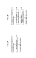
- FIG. 2A is a process diagram showing a first method of manufacturing a window material for an ultraviolet light emitting element
- FIG. 2B is a process diagram showing a second manufacturing method.
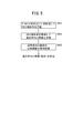
- FIG. 3A is a process diagram showing a third method of manufacturing a window material for an ultraviolet light emitting element
- FIG. 3B is a process diagram showing a fourth manufacturing method.
- FIG. 4A is a process diagram showing a fifth method of manufacturing the window material for ultraviolet light emitting elements
- FIG. 4B is a process diagram showing the sixth manufacturing method.
- FIG. 5 is process drawing which shows the 7th manufacturing method of the window material for ultraviolet light emitting elements.
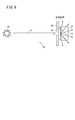
- FIG. 6 is an explanatory view showing a method of evaluating the front total light transmittance in Examples 1 to 6 and Comparative Examples 1 to 3.
- FIGS. 1 to 6 embodiments of the window material for an ultraviolet light emitting element according to the present invention and the method for manufacturing the same will be described with reference to FIGS. 1 to 6.
- “to” indicating a numerical range is used as a meaning including the numerical values described before and after it as the lower limit value and the upper limit value.
- the window material for ultraviolet light emitting element (hereinafter referred to simply as window material 10) according to the present embodiment is high in ultraviolet light 12 from an ultraviolet light emitting element (not shown) that emits ultraviolet light having a wavelength of 300 nm or less. Permeate through.
- the window member 10 is formed of an alumina substrate (light transmitting alumina substrate 14).
- the translucent alumina substrate 14 faces the surface from which the ultraviolet light 12 is emitted (the emission side surface 16a: one surface), and the surface on the side where the ultraviolet light 12 is incident (the incident side 16b: the other surface). And has a thickness t of 0.3 mm or less.
- the planar shape of each plate surface includes, for example, a triangular shape, a rectangular shape, a square shape, a circular shape, an elliptical shape, a polygonal shape, and the like depending on the shape of the case where the ultraviolet light emitting element is mounted.
- the average particle diameter of the surface of the translucent alumina substrate 14 is preferably 6 to 60 ⁇ m, more preferably 6 to 20 ⁇ m.
- the measurement method of the average particle diameter of the surface was performed as follows. That is, an arbitrary part of the surface was observed by magnifying it by 200 times with an optical microscope, and the number of crystals located on a 0.7 mm line segment was counted. Then, the value obtained by dividing the value obtained by multiplying 0.7 by 4 / ⁇ by the number of crystals is defined as the average particle size.
- the surface roughness of the emission side surface 16 a of the translucent alumina substrate 14 and the surface roughness of the incidence side surface 16 b are different.
- each surface roughness of the emission side surface 16a and the incidence side surface 16b is different. May be
- the method for producing the translucent alumina substrate 14 is not particularly limited, but any method such as a doctor blade method (tape molding method), an extrusion method, a gel cast method, etc. may be used.
- the light-transmissive alumina substrate 14 is produced by using a gel cast method or a tape forming method, and particularly preferably using a gel cast method.
- a raw material powder (ceramic powder) containing alumina powder, a slurry containing a dispersion medium and a gelling agent is cast in a mold, and the slurry is gelled to obtain a molded body.
- a translucent alumina substrate 14 is obtained (see Japanese Patent Laid-Open No. 2001-335371).
- a raw material is used in which 150 to 1000 ppm of an auxiliary is added to high purity alumina powder having a purity of 99.9% or more (preferably 99.95% or more).
- high purity alumina powder high purity alumina powder manufactured by Daimei Chemical Industry Co., Ltd. can be exemplified.
- the assistant magnesium oxide is preferable, but ZrO 2 , Y 2 O 3 , La 2 O 3 and Sc 2 O 3 can also be exemplified.
- the gel cast method includes the following methods.
- a slurry is prepared by dispersing a prepolymer such as polyvinyl alcohol as a gelling agent, an epoxy resin, a phenol resin and the like together with an inorganic powder and a dispersing agent in a dispersion medium. Thereafter, the slurry is cast into a mold and three-dimensionally crosslinked with a crosslinking agent to gelate, thereby solidifying the slurry.
- a prepolymer such as polyvinyl alcohol as a gelling agent, an epoxy resin, a phenol resin and the like
- the slurry is solidified by chemically bonding an organic dispersion medium having a reactive functional group and a gelling agent.
- This method is the method described in Japanese Patent Application Laid-Open No. 2001-335371 of the applicant.
- the window material 10 the translucent alumina substrate 14
- some manufacturing methods the first to seventh manufacturing methods of the window material 10 (the translucent alumina substrate 14) according to the present embodiment will be described with reference to the process drawings of FIGS. 2A to 5. explain.
- a raw material powder containing alumina powder, a slurry containing a dispersion medium and a gelling agent is cast in a mold, and then the slurry is cured to produce an alumina compact.
- the slurry is formed into a tape shape using a doctor blade and hardened to prepare an alumina molded body.
- step S2 the alumina compact is fired to obtain a translucent alumina substrate 14 having a thickness of 0.3 mm or less, that is, the window material 10.
- step S101 of FIG. 2B an alumina molded body is manufactured in the same manner as step S1 described above.
- step S102 the alumina compact is fired to produce a translucent alumina substrate 14 having a thickness of more than 0.3 mm.
- step S201 of FIG. 3A an alumina molded body is manufactured in the same manner as step S1 described above.
- step S202 the alumina compact is fired to produce a translucent alumina substrate 14 having a thickness of more than 0.3 mm.
- step S203 only the emission side 16a of the translucent alumina substrate 14 is mirror polished to a surface roughness Ra of 0.03 ⁇ m or less, and only the incidence side 16b of the translucent alumina substrate 14 is the surface roughness Grinding processing is performed until Ra becomes 0.2 to 0.6 ⁇ m, to obtain a translucent alumina substrate 14 having a thickness of 0.3 mm or less, ie, the window material 10.
- step S301 in FIG. 3B an alumina molded body is manufactured in the same manner as step S1 described above.
- step S302 the alumina compact is fired to produce a translucent alumina substrate 14 having a thickness of more than 0.3 mm.
- the alumina substrate 14, ie, the window material 10 is obtained.
- step S401 in FIG. 4A an alumina molded body is manufactured in the same manner as step S1 described above.
- step S402 the alumina compact is fired to prepare a translucent alumina substrate 14 having a thickness of more than 0.3 mm.
- step S501 in FIG. 4B an alumina molded body is manufactured in the same manner as step S1 described above.
- step S502 the alumina compact is fired to prepare a translucent alumina substrate 14 having a thickness of more than 0.3 mm.
- the following translucent alumina substrate 14, ie, the window material 10, is obtained.
- the following method may be employed instead of grinding the output side surface 16a and the input side surface 16b of the translucent alumina substrate 14. That is, when the alumina compact is fired in step S502, a setter having a large surface roughness is used as a setter in contact with one surface and the other surface of the alumina compact. Different types of setters may be used. As a result, the surface roughness Ra of the outgoing side surface 16a and the incoming side surface 16b of the translucent alumina substrate 14 after firing is set to 0.2 to 0.6 ⁇ m. The surface roughness of the outgoing side 16a and the incoming side 16b may be the same or different.
- step S601 in FIG. 5 an alumina molded body is manufactured in the same manner as step S1 described above.
- step S602 the alumina compact is fired to produce a translucent alumina substrate 14 having a thickness of more than 0.3 mm.
- the alumina substrate 14, ie, the window material 10 is obtained.
- the following method may be employed instead of grinding the output side surface 16 a of the translucent alumina substrate 14. That is, when firing the alumina molded body in step S602, the setter comes in contact with one surface (the surface serving as the output side surface) of the alumina molded product than the setter contacts the other surface (the surface serving as the incident side surface). Use a setter with a large surface roughness. As a result, the surface roughness Ra of the emission side surface 16a of the light-transmissive alumina substrate 14 after firing is 0.2 ⁇ m or more, preferably 0.2 to 0.6 ⁇ m.
- the translucent alumina substrate 14 is used, and the average particle diameter of the surface is 6 to 60 ⁇ m, more preferably 6 to 20 ⁇ m.
- the light transmitting alumina substrate 14 has a high thermal conductivity of 30 W / m ⁇ K or more. Therefore, it is possible to efficiently dissipate the heat generated by the drive of the ultraviolet light emitting element, and it is possible to avoid damage or deterioration due to the temperature rise in the ultraviolet light emitting element.
- the surface roughness Ra of the output side surface 16a of the translucent alumina substrate 14 is not more than 0.03 ⁇ m and the surface roughness Ra of the input side surface 16b is 0.2 to 0.6 ⁇ m.
- the surface roughness was measured and the transmittance was evaluated in Examples 1 to 6 and Comparative Examples 1 to 3.
- the breakdown and evaluation results of Examples 1 to 6 and Comparative Examples 1 to 3 are shown in Tables 1 to 3 described later.
- ⁇ Surface roughness> The surface roughness of the emission side surface and the incidence side surface of the measurement sample (Examples 1 to 6 and Comparative Examples 1 to 3) was measured at a magnification of 500 with a laser microscope (VK-9700 manufactured by Keyence Corporation).
- the front total light transmittance was used. Specifically, the average value of the transmittances at the measurement wavelength of 200 to 280 nm and the transmittance at the specific wavelength of 210 nm were used as evaluation values.
- the reason for selecting the evaluation value is that UV-C is light having a wavelength of 280 nm or less, and light having a wavelength of 200 nm or less is usually absorbed in the atmosphere, which is the measurement limit of the apparatus. Furthermore, in this example, the effect is more remarkable as the wavelength is shorter, so 210 nm is given as the specific wavelength, and the transmittance at this specific wavelength 210 nm is also used as the evaluation value.
- the total forward light transmittance was measured using a spectrophotometer 28 (manufactured by Hitachi High-Tech, U-4100) having a light source 20 and a detector 22, as shown in FIG.
- a slit plate 26 having one through hole 24 (diameter 3 mm) was installed between the light source 20 and the detector 22.
- the measurement samples (Examples 1 to 6 and Comparative Examples 1 to 3) were fixed on the surface of the slit plate 26 facing the detector 22 so as to close the through holes 24.
- the incident side surface of the measurement sample was fixed to the slit plate 26. That is, the incident side was fixed with the light source 20 side, and the emission side with the detector 22 side.
- the measurement wavelength of the spectrophotometer 28 is 175 to 2600 nm, a light source which emits ultraviolet light 12 having a wavelength of 200 to 280 nm is used as the light source 20.
- Ultraviolet light 12 having a wavelength of 200 to 280 nm is made incident from the light source 20 to the incident side of the measurement sample fixed to the slit plate 26, and the ultraviolet light 12 passing through the measurement sample and emitted from the outgoing side is detected by the detector 22.
- Example 1 According to the first production method shown in FIG. 2A, a slurry containing a ceramic powder, a dispersion medium and a gelling agent is cast in a mold, and the slurry is gelled to obtain an alumina compact, and the alumina compact is sintered. Thus, a translucent alumina substrate 14 according to Example 1 was obtained.
- magnesium oxide powder 500 ppm was added to high purity alumina powder having a purity of 99.99% or more, a BET surface area of 9 to 15 m 2 / g, and a tap density of 0.9 to 1.0 g / cm 3 .
- the raw material powder was formed by gel casting. 100 parts by weight of this powder, 40 parts by weight of dispersion medium (dimethyl malonate), 8 parts by weight of gelling agent (4,4'-diphenylmethane diisocyanate modified product), 0.1 to 0.3 parts by weight of reaction catalyst (triethylamine) Part, a nonionic dispersant was mixed.
- the raw material powder and the dispersing agent were added to the dispersing medium and dispersed at 20 ° C., and then the gelling agent was added and dispersed, and finally, the reaction catalyst was added to prepare a slurry.
- the slurry was cast in a mold and left to gel for 2 hours.
- the gelled alumina compact was removed from the mold and dried at 60 to 100.degree.
- the compact was then degreased at 1100 ° C. for 2 hours and fired in a hydrogen atmosphere.
- the thickness t of the translucent alumina substrate 14 was 0.3 mm, and the average particle diameter of the surface was 20 ⁇ m. Further, the surface roughness Ra of both the emission side surface 16a and the incidence side surface 16b was 0.3 ⁇ m.
- the average of the transmittance in the wavelength region of 200 to 280 nm was 89%, and 90% at the wavelength of 210 nm.
- Example 2 A translucent alumina substrate 14 according to Example 2 was produced in the same manner as in Example 1 except that the average particle diameter (or the firing temperature or the firing time) of the alumina powder was changed.
- Example 3 A translucent alumina substrate 14 according to Example 3 was obtained according to the second manufacturing method shown in FIG. 2B.
- a translucent alumina substrate 14 having a thickness of 0.5 mm was produced by the same method as in Example 1 described above.
- mirror polishing was performed only on the emission side surface 16a of the translucent alumina substrate 14 to obtain a translucent alumina substrate 14 according to Example 3 with a thickness of 0.3 mm.
- the average particle diameter of the surface of the translucent alumina substrate 14 before mirror polishing was 20 ⁇ m, and the surface roughness Ra of both the emission side surface 16 a and the incidence side surface 16 b was 0.3 ⁇ m.
- the surface roughness Ra of the emission side surface 16a of the translucent alumina substrate 14 after mirror polishing was 0.03 ⁇ m. Then, when the forward total light transmittance was measured, the average of the transmittance in the wavelength region of 200 to 280 nm was 91%, and it was 96% at the wavelength of 210 nm.
- Example 4 A translucent alumina substrate 14 according to Example 4 was obtained according to the third manufacturing method shown in FIG. 3A. Specifically, first, a translucent alumina substrate 14 having a thickness of 0.5 mm was produced by the same method as in Example 1 described above. Thereafter, mirror polishing is performed only on the emission side surface 16a of the translucent alumina substrate 14, and only the incident side surface 16b is subjected to grinding treatment (treatment to roughen the surface: rough surface treatment) with a grindstone to a thickness of 0.3 mm A translucent alumina substrate 14 according to Example 4 was obtained. The average particle diameter of the surface of the translucent alumina substrate 14 before mirror polishing and roughening was 20 ⁇ m.
- the surface roughness Ra of the light-emitting side surface 16a of the translucent alumina substrate 14 was 0.03 ⁇ m, and the surface roughness Ra of the light-receiving side surface 16b was 0.6 ⁇ m. Then, when the total front light transmittance was measured, the average of the transmittance in the wavelength region of 200 to 280 nm was 92%, and it was 97% at the wavelength of 210 nm.
- Example 6 A translucent alumina substrate 14 according to Example 6 was obtained according to the fifth manufacturing method shown in FIG. 4A. Specifically, first, a translucent alumina substrate 14 having a thickness of 0.5 mm was produced by the same method as in Example 1 described above. Thereafter, mirror polishing was performed only on the incident side surface 16b of the translucent alumina substrate 14 contrary to the third embodiment, to obtain the translucent alumina substrate 14 according to the sixth embodiment with a thickness of 0.3 mm. The average particle diameter of the surface of the translucent alumina substrate 14 before mirror polishing was 20 ⁇ m, and the surface roughness Ra of both the emission side surface 16 a and the incidence side surface 16 b was 0.3 ⁇ m.
- the surface roughness Ra of the incident side surface 16b of the translucent alumina substrate 14 after the mirror polishing was 0.03 ⁇ m. Then, when the total front light transmittance was measured, the average of the transmittance in the wavelength region of 200 to 280 nm was 87%, and 91% at the wavelength of 210 nm.
- Comparative example 2 A translucent alumina substrate 14 according to Comparative Example 2 was produced in the same manner as in Example 1 except that the average particle diameter (or the firing temperature or the firing time) of the alumina powder was changed.
- the thickness t of the translucent alumina substrate 14 was 0.3 mm, the average particle diameter of the surface was 5 ⁇ m, and the surface roughness Ra of both the emission side surface 16 a and the incidence side surface 16 b was 0.1 ⁇ m. Then, when the total front light transmittance was measured, the average of the transmittance in the wavelength region of 200 to 280 nm was 67%, and it was 68% at the wavelength of 210 nm.
- Comparative example 3 A translucent alumina substrate 14 according to Comparative Example 3 was produced in the same manner as in Example 1 except that the average particle diameter (or the firing temperature or the firing time) of the alumina powder was changed.
- the thickness t of the translucent alumina substrate 14 was 0.3 mm, and the average particle diameter of the surface was 65 ⁇ m.
- production of the crack was seen. Therefore, the surface roughness and the front total light transmittance could not be measured.
- the window material 10 is preferably made of translucent alumina, and the average particle diameter of the surface is preferably 6 to 60 ⁇ m.
- the evaluation of the front total light transmittance is better than that of Example 5, but the thermal conductivity is as low as about 1 W / m ⁇ K, so heat can not be dissipated efficiently. There is a concern that damage and deterioration are likely to occur due to the temperature rise of the ultraviolet light emitting element.
- the window material for an ultraviolet light emitting element according to the present invention and the method of manufacturing the same are not limited to the above-described embodiment, and it goes without saying that various configurations can be adopted without departing from the scope of the present invention.
Landscapes
- Engineering & Computer Science (AREA)
- Chemical & Material Sciences (AREA)
- Ceramic Engineering (AREA)
- Manufacturing & Machinery (AREA)
- Physics & Mathematics (AREA)
- Materials Engineering (AREA)
- Structural Engineering (AREA)
- Organic Chemistry (AREA)
- Inorganic Chemistry (AREA)
- Optics & Photonics (AREA)
- General Physics & Mathematics (AREA)
- Mechanical Engineering (AREA)
- Thermal Sciences (AREA)
- Dispersion Chemistry (AREA)
- Geometry (AREA)
- Led Device Packages (AREA)
- Compositions Of Oxide Ceramics (AREA)
Abstract
L'invention concerne un matériau de fenêtre pour un élément d'émission de rayons ultraviolets, ainsi qu'un procédé de production associé. Le matériau de fenêtre (10) est destiné à être utilisé dans un élément d'émission de rayons ultraviolets et il est disposé sur au moins le côté émission d'un élément d'émission de rayons ultraviolets pour émettre un rayonnement ultraviolet (12) d'une longueur d'onde de 300nm ou inférieure. Le matériau de fenêtre (10) pour élément d'émission de rayons ultraviolets comprend un substrat d'alumine à transmission de lumière (14) et le diamètre moyen des particules de la surface de ce substrat est compris entre 6 et 60μm. Ainsi, le matériau de fenêtre (10) selon l'invention présente une conductivité thermique élevée, peut assurer une vitesse de transmission élevée, de 300nm ou inférieure, de rayons ultraviolets, et est adapté pour être utilisé dans un élément d'émission de rayons ultraviolets.
Priority Applications (3)
| Application Number | Priority Date | Filing Date | Title |
|---|---|---|---|
| JP2015522782A JP6326412B2 (ja) | 2013-06-12 | 2014-06-10 | 紫外線発光素子用窓材及びその製造方法 |
| EP14810788.1A EP3010051B1 (fr) | 2013-06-12 | 2014-06-10 | Matériau de fenêtre pour élément d'émission de rayons ultraviolets et procédé de production associé |
| US14/965,546 US20160096776A1 (en) | 2013-06-12 | 2015-12-10 | Window material for ultraviolet-ray-emitting element and method for producing same |
Applications Claiming Priority (2)
| Application Number | Priority Date | Filing Date | Title |
|---|---|---|---|
| JP2013-123466 | 2013-06-12 | ||
| JP2013123466 | 2013-06-12 |
Related Child Applications (1)
| Application Number | Title | Priority Date | Filing Date |
|---|---|---|---|
| US14/965,546 Continuation US20160096776A1 (en) | 2013-06-12 | 2015-12-10 | Window material for ultraviolet-ray-emitting element and method for producing same |
Publications (1)
| Publication Number | Publication Date |
|---|---|
| WO2014199975A1 true WO2014199975A1 (fr) | 2014-12-18 |
Family
ID=52022267
Family Applications (1)
| Application Number | Title | Priority Date | Filing Date |
|---|---|---|---|
| PCT/JP2014/065317 Ceased WO2014199975A1 (fr) | 2013-06-12 | 2014-06-10 | Matériau de fenêtre pour élément d'émission de rayons ultraviolets et procédé de production associé |
Country Status (4)
| Country | Link |
|---|---|
| US (1) | US20160096776A1 (fr) |
| EP (1) | EP3010051B1 (fr) |
| JP (1) | JP6326412B2 (fr) |
| WO (1) | WO2014199975A1 (fr) |
Cited By (2)
| Publication number | Priority date | Publication date | Assignee | Title |
|---|---|---|---|---|
| US9287106B1 (en) | 2014-11-10 | 2016-03-15 | Corning Incorporated | Translucent alumina filaments and tape cast methods for making |
| KR20190135023A (ko) | 2017-03-30 | 2019-12-05 | 엔지케이 인슐레이터 엘티디 | 가고정 기판 및 전자 부품의 몰드 방법 |
Families Citing this family (1)
| Publication number | Priority date | Publication date | Assignee | Title |
|---|---|---|---|---|
| JP6623968B2 (ja) | 2016-08-03 | 2019-12-25 | 信越化学工業株式会社 | 光学素子パッケージ用窓材、光学素子パッケージ、それらの製造方法、及び光学素子用パッケージ |
Citations (9)
| Publication number | Priority date | Publication date | Assignee | Title |
|---|---|---|---|---|
| JPH03285865A (ja) * | 1990-03-30 | 1991-12-17 | Kyocera Corp | 透光性アルミナセラミックスおよびその製造方法 |
| JPH1072684A (ja) * | 1996-06-11 | 1998-03-17 | Ngk Insulators Ltd | プラズマ生成用ガス通過管 |
| JP2000349348A (ja) | 1999-03-31 | 2000-12-15 | Toyoda Gosei Co Ltd | 短波長ledランプユニット |
| JP2001335371A (ja) | 2000-03-22 | 2001-12-04 | Ngk Insulators Ltd | 粉体成形体の製造方法 |
| JP2002289925A (ja) | 2001-03-23 | 2002-10-04 | Citizen Electronics Co Ltd | 発光ダイオード |
| JP2007043487A (ja) * | 2005-08-03 | 2007-02-15 | Ngk Insulators Ltd | 圧電振動子の振動周波数調整用の蓋材および圧電振動子収容構造 |
| JP2007324220A (ja) * | 2006-05-30 | 2007-12-13 | Toshiba Corp | 光半導体装置 |
| JP2008091623A (ja) | 2006-10-02 | 2008-04-17 | Miyata Ind Co Ltd | 発光装置 |
| JP2012238654A (ja) * | 2011-05-10 | 2012-12-06 | Ngk Insulators Ltd | 透光性配線基板およびその製造方法 |
Family Cites Families (6)
| Publication number | Priority date | Publication date | Assignee | Title |
|---|---|---|---|---|
| JP2005166454A (ja) * | 2003-12-03 | 2005-06-23 | Tokuyama Corp | 光源用カバー |
| JP4020092B2 (ja) * | 2004-03-16 | 2007-12-12 | 住友電気工業株式会社 | 半導体発光装置 |
| JP2008053702A (ja) * | 2006-07-26 | 2008-03-06 | Kyocera Corp | 発光装置および照明装置 |
| JP5650885B2 (ja) * | 2008-12-27 | 2015-01-07 | 日亜化学工業株式会社 | 波長変換焼結体及びこれを用いた発光装置、並びに波長変換焼結体の製造方法 |
| US8278233B2 (en) * | 2009-09-09 | 2012-10-02 | Ngk Insulators, Ltd. | Translucent polycrystalline sintered body, method for producing the same, and arc tube for high-intensity discharge lamp |
| KR101570958B1 (ko) * | 2013-12-25 | 2015-11-20 | 엔지케이 인슐레이터 엘티디 | 핸들 기판, 반도체용 복합 기판, 반도체 회로 기판 및 그 제조 방법 |
-
2014
- 2014-06-10 WO PCT/JP2014/065317 patent/WO2014199975A1/fr not_active Ceased
- 2014-06-10 JP JP2015522782A patent/JP6326412B2/ja active Active
- 2014-06-10 EP EP14810788.1A patent/EP3010051B1/fr active Active
-
2015
- 2015-12-10 US US14/965,546 patent/US20160096776A1/en not_active Abandoned
Patent Citations (9)
| Publication number | Priority date | Publication date | Assignee | Title |
|---|---|---|---|---|
| JPH03285865A (ja) * | 1990-03-30 | 1991-12-17 | Kyocera Corp | 透光性アルミナセラミックスおよびその製造方法 |
| JPH1072684A (ja) * | 1996-06-11 | 1998-03-17 | Ngk Insulators Ltd | プラズマ生成用ガス通過管 |
| JP2000349348A (ja) | 1999-03-31 | 2000-12-15 | Toyoda Gosei Co Ltd | 短波長ledランプユニット |
| JP2001335371A (ja) | 2000-03-22 | 2001-12-04 | Ngk Insulators Ltd | 粉体成形体の製造方法 |
| JP2002289925A (ja) | 2001-03-23 | 2002-10-04 | Citizen Electronics Co Ltd | 発光ダイオード |
| JP2007043487A (ja) * | 2005-08-03 | 2007-02-15 | Ngk Insulators Ltd | 圧電振動子の振動周波数調整用の蓋材および圧電振動子収容構造 |
| JP2007324220A (ja) * | 2006-05-30 | 2007-12-13 | Toshiba Corp | 光半導体装置 |
| JP2008091623A (ja) | 2006-10-02 | 2008-04-17 | Miyata Ind Co Ltd | 発光装置 |
| JP2012238654A (ja) * | 2011-05-10 | 2012-12-06 | Ngk Insulators Ltd | 透光性配線基板およびその製造方法 |
Non-Patent Citations (1)
| Title |
|---|
| See also references of EP3010051A4 |
Cited By (2)
| Publication number | Priority date | Publication date | Assignee | Title |
|---|---|---|---|---|
| US9287106B1 (en) | 2014-11-10 | 2016-03-15 | Corning Incorporated | Translucent alumina filaments and tape cast methods for making |
| KR20190135023A (ko) | 2017-03-30 | 2019-12-05 | 엔지케이 인슐레이터 엘티디 | 가고정 기판 및 전자 부품의 몰드 방법 |
Also Published As
| Publication number | Publication date |
|---|---|
| US20160096776A1 (en) | 2016-04-07 |
| JPWO2014199975A1 (ja) | 2017-02-23 |
| JP6326412B2 (ja) | 2018-05-16 |
| EP3010051A1 (fr) | 2016-04-20 |
| EP3010051B1 (fr) | 2020-01-08 |
| EP3010051A4 (fr) | 2017-02-22 |
Similar Documents
| Publication | Publication Date | Title |
|---|---|---|
| KR101657876B1 (ko) | 파장 변환 소성체 | |
| US11402077B2 (en) | Fluorescent member and light-emitting module | |
| EP1979954B1 (fr) | Dispositif emetteur de lumiere | |
| CN103703542B (zh) | 复合晶片及其制造方法 | |
| JP5709463B2 (ja) | 光源装置および照明装置 | |
| JP2014207436A (ja) | 波長変換体 | |
| WO2015172670A1 (fr) | Dispositif de conversion de longueur d'onde, système source de lumière et système de projection | |
| JP2012064484A (ja) | 光源装置 | |
| KR20180052560A (ko) | 파장 변환 부재 및 발광 디바이스 | |
| JP2016157905A (ja) | 光学部品 | |
| JP2012089316A (ja) | 光源装置および照明装置 | |
| EP2436047A2 (fr) | Plaque de diffusion et de conversion de lumière pour del | |
| WO2017208855A1 (fr) | Élément en verre de silice pour scellement hermétique d'un élément à led smd ultraviolette et procédé de fabrication d'un élément en verre de quartz pour led ultraviolette | |
| TW202432794A (zh) | 波長轉換元件、製造其之方法、光轉換裝置、及產生白光的方法 | |
| JP6326412B2 (ja) | 紫外線発光素子用窓材及びその製造方法 | |
| EP2998768A1 (fr) | Composant optique | |
| JP2015121763A (ja) | 光学部品 | |
| JP5917183B2 (ja) | 光源装置および照明装置 | |
| CN119846891B (zh) | 用于波长转换装置的耐高温反射层 | |
| JP2012238654A (ja) | 透光性配線基板およびその製造方法 | |
| JP6375188B2 (ja) | 透光性焼結セラミック支持体及びその製造方法 | |
| KR20180063541A (ko) | 다결정 형광막 및 그 제조 방법 및 그를 이용한 차량 램프 장치 | |
| Wan et al. | Laser-drilled microstructures for enhanced luminous efficiency and wide-angle emission in WLEDs | |
| JP2020187205A (ja) | 光波長変換部材、および、発光装置 | |
| JP2011211024A (ja) | 光半導体素子用パッケージ向け光反射セラミック材およびそれを用いた光半導体素子用パッケージ |
Legal Events
| Date | Code | Title | Description |
|---|---|---|---|
| 121 | Ep: the epo has been informed by wipo that ep was designated in this application |
Ref document number: 14810788 Country of ref document: EP Kind code of ref document: A1 |
|
| ENP | Entry into the national phase |
Ref document number: 2015522782 Country of ref document: JP Kind code of ref document: A |
|
| WWE | Wipo information: entry into national phase |
Ref document number: 2014810788 Country of ref document: EP |
|
| NENP | Non-entry into the national phase |
Ref country code: DE |