WO2014203682A1 - 2ポートトリプレート線路-導波管変換器 - Google Patents
2ポートトリプレート線路-導波管変換器 Download PDFInfo
- Publication number
- WO2014203682A1 WO2014203682A1 PCT/JP2014/063684 JP2014063684W WO2014203682A1 WO 2014203682 A1 WO2014203682 A1 WO 2014203682A1 JP 2014063684 W JP2014063684 W JP 2014063684W WO 2014203682 A1 WO2014203682 A1 WO 2014203682A1
- Authority
- WO
- WIPO (PCT)
- Prior art keywords
- waveguide
- triplate
- probes
- line
- rectangular waveguide
- Prior art date
- Legal status (The legal status is an assumption and is not a legal conclusion. Google has not performed a legal analysis and makes no representation as to the accuracy of the status listed.)
- Ceased
Links
Images



Classifications
-
- H—ELECTRICITY
- H01—ELECTRIC ELEMENTS
- H01P—WAVEGUIDES; RESONATORS, LINES, OR OTHER DEVICES OF THE WAVEGUIDE TYPE
- H01P5/00—Coupling devices of the waveguide type
- H01P5/08—Coupling devices of the waveguide type for linking dissimilar lines or devices
- H01P5/10—Coupling devices of the waveguide type for linking dissimilar lines or devices for coupling balanced lines or devices with unbalanced lines or devices
- H01P5/107—Hollow-waveguide/strip-line transitions
-
- H—ELECTRICITY
- H01—ELECTRIC ELEMENTS
- H01P—WAVEGUIDES; RESONATORS, LINES, OR OTHER DEVICES OF THE WAVEGUIDE TYPE
- H01P3/00—Waveguides; Transmission lines of the waveguide type
- H01P3/12—Hollow waveguides
-
- H—ELECTRICITY
- H01—ELECTRIC ELEMENTS
- H01P—WAVEGUIDES; RESONATORS, LINES, OR OTHER DEVICES OF THE WAVEGUIDE TYPE
- H01P5/00—Coupling devices of the waveguide type
- H01P5/12—Coupling devices having more than two ports
-
- H—ELECTRICITY
- H01—ELECTRIC ELEMENTS
- H01Q—ANTENNAS, i.e. RADIO AERIALS
- H01Q9/00—Electrically-short antennas having dimensions not more than twice the operating wavelength and consisting of conductive active radiating elements
- H01Q9/04—Resonant antennas
- H01Q9/30—Resonant antennas with feed to end of elongated active element, e.g. unipole
- H01Q9/42—Resonant antennas with feed to end of elongated active element, e.g. unipole with folded element, the folded parts being spaced apart a small fraction of the operating wavelength
-
- H—ELECTRICITY
- H01—ELECTRIC ELEMENTS
- H01Q—ANTENNAS, i.e. RADIO AERIALS
- H01Q21/00—Antenna arrays or systems
- H01Q21/06—Arrays of individually energised antenna units similarly polarised and spaced apart
- H01Q21/061—Two dimensional planar arrays
Definitions
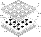
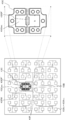
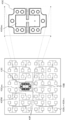
- a conventional triplate feed type planar antenna is composed of a ground plate 41, a foam sheet 42-1, a flexible substrate 43, a foam sheet 42-2 and a slot plate 44, for example, as shown in FIG.
- the elements stacked in this way are configured as follows.
- a pattern corresponding to a plain ground is formed on the upper surface of the ground plate 41.
- a waveguide-triplate line converter (hereinafter simply referred to as “converter”) 43C is disposed at a predetermined portion surrounded by the patch antennas 43A 1,1 to 43A m, n on the flexible substrate 43.
- one end is connected to the probe 43CP inserted into the tube from the side wall of the waveguide 43C WC constituting the converter 43C, and the bus line of the power supply path 43F that realizes the tournament power supply described above.
- a trunk line 43B having the other end connected to 43FM is formed.
- the “electromagnetic field of the triplate line” is led to a point deviated by a distance corresponding to (1 ⁇ 4) wavelength from the center of the bus 43FM, and the patch antenna 43A 1, Tournament power is fed to each of half of 1 to 43A m, n and the other half with a phase difference of 180 degrees.
- the cross polarization components of the patch antennas 43A 1,1 to 43A m, n and the remaining half cancel each other as two components having opposite phases. Therefore, the cross polarization discrimination degree is improved.
- Patent Document 1 states that “a ground conductor 11, a dielectric 10, a feeding substrate 9 in which a plurality of radiating elements 7 and a feeding line 8 are formed, a dielectric 6, and each slot 12 are directly above the radiating element 7.
- a ground conductor 1 having a plurality of slots 12 disposed so as to be positioned, a dielectric 2, a power supply substrate 5 having a plurality of radiating elements 3 and a feed line 4, a dielectric 13 and each slot 14 are radiated.
- a ground conductor 15 having a plurality of slots 14 installed so as to be positioned immediately above the element 3 is stacked in this order, the radiating element 3 and the radiating element 7 are electromagnetically coupled, and the radiating element by the feed line 4 3 and the excitation direction of the radiating element 7 by the feed line 8 are orthogonal to each other.
- the number of elements is about half that of the array elements of the feed board 5 and the feed board 9.
- Radiating element And radiating elements and feed lines corresponding to about half the number of elements arranged on the feed line or any one of the feed boards are spatially rotated 180 degrees with respect to the reference excitation direction and electrically “Excitation by changing the feeding phase by 180 degrees” is characterized by having “cross-polarization characteristics and broadband characteristics of isolation in order to reduce the burden on the signal processing circuit as much as possible on the planar antenna side”.
- a dual polarization planar antenna is disclosed.
- Patent Document 2 states that “a substrate provided with a microstrip line so that an antenna probe is positioned opposite to an opening of a waveguide is placed between a cap corresponding to the opening of the waveguide and a base member.
- the antenna probe is attached to the substrate in a configuration in which the microstrip line is connected to both ends of the antenna probe.
- a waveguide / microstrip line converter characterized in that it also has a function of distributing the power supply from the antenna probe is disclosed.
- Patent Document 3 states that “a strip plate formed on a substrate is a triplate configuration in which a gap is sandwiched between grounded substrates from both sides, and a radiating element is formed on one of the grounded substrates.
- a planar antenna that feeds power in parallel with a feed line, the strip line at the final connection point is inserted from both sides of the waveguide, and the phase difference between the power input to the waveguide from both strip lines is 180 °.
- the stripline-waveguide converter is formed in the empty space between the radiating elements formed at equal intervals in the vertical and horizontal directions.
- a planar antenna is disclosed that is characterized in that “feeding is possible”.
- the aforementioned phase difference of 180 degrees is ensured by connecting the main line 43B to a point that is deviated by (1 ⁇ 4) wavelength from the center of the bus bar 43FM.
- the frequency of the radio signal to be transmitted or received has a wide range of values, or when the radio signal has a wide occupied band (for example, 2 GHz in the 12 GHz band), it is difficult to set with sufficient accuracy. .
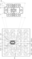
- phase difference error can be reduced by, for example, the following configuration as shown in FIG.
- a probe 43CP ′ instead of the probe 43CP is disposed at a portion corresponding to the central portion of the waveguide 43C WC .
- the probe 43CP ′ is interposed in the center of the trunk line 43B.
- FIG. 9 and FIG. 10 are often not applied due to restrictions on frequency, waveguide 43C WC, and other physical dimensions, shapes, and arrangements.
- the two-port triplate line-waveguide converter is individually formed on the rectangular waveguide and two opposing inner walls of the rectangular waveguide, and the two Two probes connected to the central conductor of each individual triplate line via a slit having an opening on a virtual straight line orthogonal to the inner wall, and the two probes have tips at the rectangular waveguide And a monopole antenna that functions as a ground plate.
- the two probes are bent in a rectangular waveguide, thereby reducing or suppressing unnecessary coupling between them, and by functioning as the monopole antenna, the electromagnetic field in the tube is spread over a wide band.
- Two opposite-phase ports to be coupled are formed between individual triplate lines.
- a two-port triplate line-waveguide converter is formed separately on a rectangular waveguide and two opposing inner walls of the rectangular waveguide, and the two Two probes connected to the central conductor of each individual triplate line via a slit having an opening on a virtual straight line orthogonal to the inner wall, and the two probes have tips at the rectangular waveguide And a monopole antenna that branches in a plurality of directions and functions as a ground plate.
- the two probes branch in a plurality of directions within the rectangular waveguide, thereby reducing or suppressing unnecessary coupling between them, and by functioning as the monopole antenna, it is possible to widen the electromagnetic field in the tube.
- Two anti-phase ports that are coupled to each other are formed between individual triplate lines.
- the two-port triplate line-waveguide converter is formed on the two opposing inner walls of the rectangular waveguide, and is virtually formed perpendicular to the two inner walls.
- Two probes connected to the central conductor of each individual triplate line through a slit having an opening on a straight line, and the two probes do not oppose each other inside the rectangular waveguide
- the monopole antenna is bent in the direction and functions as a ground plate with the inner wall.
- the two probes are bent in a direction in which the tip portions do not face each other in the rectangular waveguide, thereby reducing or suppressing unnecessary coupling between them, and by functioning as the monopole antenna, Two anti-phase ports that couple to the electromagnetic field over a wide band are formed between the individual triplate lines.
- the signal between the rectangular waveguide and the two triplate lines is out of phase without significant change in configuration and large dependence on the frequency. Delivery is realized in parallel.
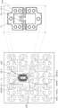
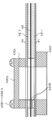
- FIG. 1 is a diagram showing an embodiment of the present invention.
- the trunk line 43B is not provided.
- Two probes 12-1 and 12-2 configured as follows are provided in place of the probe 43CP.
- L ⁇ / 4
- the saddle length L1 is determined by the degree of coupling between the electromagnetic field in the waveguide 11 and the probe 12-1 (12-2) and the probe 12-1, 12-2. It is set in the balance with the isolation that should be secured in between.
- the probes 12-1 and 12-2 each function as a monopole antenna in the waveguide 11 having the side wall of the waveguide 11 as a ground plate. To do.
- phase of the electromagnetic field coupled to the probes 12-1 and 12-2 in the waveguide 11 is 180 degrees opposite to each other.
- the half and the other half of the patch antennas 43A 1,1 to 43A m, n are a two-port waveguide composed of the waveguide 11 and the probes 12-1 and 12-2 as described above. -Powered in reverse phase in parallel by a triplate line converter.
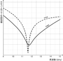
- the main lobe shift which was about 0.3 degrees in the conventional example, is suppressed to within 0.1 degrees. It is done.
- the probes 12-1 and 12-2 achieve the isolation between the probes 12-1 and 12-2 and the overall power supply efficiency within desired limits. If it is, it will not be limited to the aspect shown in FIG. 1, You may comprise in any form listed below.
- the tip branches off into a T shape instead of an L shape so as to function as a T-shaped monopole antenna.
- the tip of the eaves branches into 3 or more.
- the direction in which the tip of the heel is branched is not limited to the pattern surface of the flexible substrate 43, but is set to a direction that intersects the pattern surface of the flexible substrate 43 within the scope of cost constraints and technical feasibility. .
- bus bars 43FM-1 and 43FM-2 which are the central conductors of the triplate line outside the waveguide 11, and on a surface different from the bus bars 43FM-1 and 43FM-2 on the flexible substrate 43. It is formed.
- the number of patch antennas to be fed in opposite phases may be any value.
- the present invention is not limited to a triplate-fed type planar antenna, and a device in which coupling between a waveguide and two triplate lines should be realized in a stable and reverse phase over a wide band. Any system can be applied.
- the present invention is not limited to a polarization-only planar antenna that forms a radio transmission path with a common polarization in the uplink and the downlink, for example, as shown in FIG.
- the present invention can be similarly applied to a dual-polarization type planar antenna formed by polarized waves orthogonal to each other.
- the present invention can be widely applied to a two-port triplate line-waveguide converter having two ports coupled to electromagnetic fields in a rectangular waveguide and transferring the electromagnetic fields to a triplate line connected to these ports. .
- the signal between the rectangular waveguide and the two triplate lines is out of phase without significant change in configuration and large dependence on the frequency. Delivery is realized in parallel.
- the technical problem caused by the lack of accuracy of the reverse phase or the change in the performance occurs without causing any major obstacles or restrictions on cost, mounting, temperature, power consumption, etc. Is avoided with high accuracy.
Landscapes
- Waveguide Aerials (AREA)
- Variable-Direction Aerials And Aerial Arrays (AREA)
- Waveguide Switches, Polarizers, And Phase Shifters (AREA)
- Testing Or Measuring Of Semiconductors Or The Like (AREA)
Abstract
Description
本願は、2013年6月18日に、日本に出願された特願2013-127069号に基づき優先権を主張し、その内容をここに援用する。
L=L1+L2
L=λ/4
12,43CP プローブ
41 グランド板
42 発泡シート
43 フレキシブル基板
43A パッチアンテナ
43B 幹線路
43C 導波管-トリプレート線路変換器
43CF 導波管フランジ
43CR 環状部材
43Cr 環状部材
43Cs ショート板
43F 給電路
43FM 母線
44 スロット板
44S スロット開口
Claims (3)
- 矩形導波管と、
前記矩形導波管の対向する2つの内壁に個別に形成され、かつ前記2つの内壁に直交する仮想的な直線上に開口部を有するスリットを介して、個別のトリプレート線路の中心導体に連なる2つのプローブとを備え、
前記2つのプローブは、
先端部が前記矩形導波管の内部で屈曲し、かつ前記内壁を接地板として機能するモノポールアンテナとして構成された
ことを特徴とする2ポートトリプレート線路-導波管変換器。 - 矩形導波管と、
前記矩形導波管の対向する2つの内壁に個別に形成され、かつ前記2つの内壁に直交する仮想的な直線上に開口部を有するスリットを介して、個別のトリプレート線路の中心導体に連なる2つのプローブとを備え、
前記2つのプローブは、
先端部が前記矩形導波管の内部で複数方向に分岐し、かつ前記内壁を接地板として機能するモノポールアンテナとして構成された
ことを特徴とする2ポートトリプレート線路-導波管変換器。 - 前記矩形導波管の対向する2つの内壁に個別に形成され、かつ前記2つの内壁に直交する仮想的な直線上に開口部を有するスリットを介して、個別のトリプレート線路の中心導体に連なる2つのプローブとを備え、
前記2つのプローブは、
先端部が前記矩形導波管の内部で互いに対向しない方向に屈曲し、かつ前記内壁を接地板として機能するモノポールアンテナとして構成された
ことを特徴とする2ポートトリプレート線路-導波管変換器。
Priority Applications (4)
| Application Number | Priority Date | Filing Date | Title |
|---|---|---|---|
| US14/898,733 US10003117B2 (en) | 2013-06-18 | 2014-05-23 | Two-port triplate-line/waveguide converter having two probes with tips extending in different directions |
| BR112015031224-1A BR112015031224B1 (pt) | 2013-06-18 | 2014-05-23 | Conversor de duas portas de linha de três placas/guia de onda |
| EP14813011.5A EP3012899A4 (en) | 2013-06-18 | 2014-05-23 | Two-port triplate-line/waveguide converter |
| PH12015502758A PH12015502758B1 (en) | 2013-06-18 | 2015-12-10 | Two-port triplate-line / waveguide converter |
Applications Claiming Priority (2)
| Application Number | Priority Date | Filing Date | Title |
|---|---|---|---|
| JP2013127069A JP6318392B2 (ja) | 2013-06-18 | 2013-06-18 | 2ポートトリプレート線路−導波管変換器 |
| JP2013-127069 | 2013-06-18 |
Publications (1)
| Publication Number | Publication Date |
|---|---|
| WO2014203682A1 true WO2014203682A1 (ja) | 2014-12-24 |
Family
ID=52104424
Family Applications (1)
| Application Number | Title | Priority Date | Filing Date |
|---|---|---|---|
| PCT/JP2014/063684 Ceased WO2014203682A1 (ja) | 2013-06-18 | 2014-05-23 | 2ポートトリプレート線路-導波管変換器 |
Country Status (7)
| Country | Link |
|---|---|
| US (1) | US10003117B2 (ja) |
| EP (1) | EP3012899A4 (ja) |
| JP (1) | JP6318392B2 (ja) |
| BR (1) | BR112015031224B1 (ja) |
| CL (1) | CL2015003622A1 (ja) |
| PH (1) | PH12015502758B1 (ja) |
| WO (1) | WO2014203682A1 (ja) |
Cited By (1)
| Publication number | Priority date | Publication date | Assignee | Title |
|---|---|---|---|---|
| WO2017017844A1 (ja) * | 2015-07-30 | 2017-02-02 | 三菱電機株式会社 | 給電回路 |
Families Citing this family (11)
| Publication number | Priority date | Publication date | Assignee | Title |
|---|---|---|---|---|
| JP6721352B2 (ja) * | 2015-03-23 | 2020-07-15 | 日本無線株式会社 | 導波管/伝送線路変換器及びアンテナ装置 |
| US10270186B2 (en) * | 2015-08-31 | 2019-04-23 | Kabushiki Kaisha Toshiba | Antenna module and electronic device |
| WO2017131099A1 (en) * | 2016-01-29 | 2017-08-03 | Nidec Elesys Corporation | Waveguide device, and antenna device including the waveguide device |
| JP6925153B2 (ja) * | 2017-04-06 | 2021-08-25 | 日本無線株式会社 | トリプレート型平面アンテナ |
| US10530047B2 (en) | 2017-05-24 | 2020-01-07 | Waymo Llc | Broadband waveguide launch designs on single layer PCB |
| WO2019138468A1 (ja) * | 2018-01-10 | 2019-07-18 | 三菱電機株式会社 | 導波管マイクロストリップ線路変換器およびアンテナ装置 |
| CN110137650B (zh) * | 2019-05-05 | 2021-08-10 | 苏州大学 | 波导装置及信号传输装置 |
| US11923625B2 (en) * | 2019-06-10 | 2024-03-05 | Atcodi Co., Ltd | Patch antenna and array antenna comprising same |
| US12272857B2 (en) | 2020-03-06 | 2025-04-08 | Mitsubishi Electric Corporation | Waveguide microstrip line converter |
| CN112103608B (zh) * | 2020-09-29 | 2022-02-22 | 中国航空工业集团公司雷华电子技术研究所 | 一种高隔离度的功分功合器 |
| EP4120470A1 (en) * | 2021-07-15 | 2023-01-18 | ALCAN Systems GmbH | Radio frequency device |
Citations (5)
| Publication number | Priority date | Publication date | Assignee | Title |
|---|---|---|---|---|
| JPH02171006A (ja) * | 1988-12-23 | 1990-07-02 | Matsushita Electric Works Ltd | 平面アンテナ |
| JPH09312515A (ja) | 1996-05-22 | 1997-12-02 | Hitachi Chem Co Ltd | 偏波共用平面アンテナ |
| JPH11312909A (ja) | 1998-04-28 | 1999-11-09 | Nec Corp | 導波管/マイクロストリップライン変換器およびそれを有するマイクロストリップアレイアンテナ |
| JP2012175181A (ja) * | 2011-02-17 | 2012-09-10 | Japan Radio Co Ltd | 導波管伝送線路変換器 |
| JP2012526429A (ja) * | 2009-05-08 | 2012-10-25 | テレフオンアクチーボラゲット エル エム エリクソン(パブル) | チップから導波管ポートへの変換器 |
Family Cites Families (19)
| Publication number | Priority date | Publication date | Assignee | Title |
|---|---|---|---|---|
| CA2059364A1 (en) | 1991-01-30 | 1992-07-31 | Eric C. Kohls | Waveguide transition for flat plate antenna |
| FR2675637B1 (fr) | 1991-04-16 | 1993-07-09 | Bretagne Critt | Transition ligne microruban/guide d'ondes. |
| JP2582964B2 (ja) | 1991-08-14 | 1997-02-19 | 松下電工株式会社 | 平面アンテナ |
| JPH0752803A (ja) | 1993-08-12 | 1995-02-28 | Toshiba Corp | 運転整理支援装置 |
| US5394119A (en) | 1993-08-24 | 1995-02-28 | Raytheon Company | Radio frequency connector for a patch coupled aperture array antenna |
| JPH08293706A (ja) * | 1995-02-24 | 1996-11-05 | New Japan Radio Co Ltd | 板状アンテナとコンバータの接続構造 |
| US5539361A (en) | 1995-05-31 | 1996-07-23 | The United States Of America As Represented By The Secretary Of The Air Force | Electromagnetic wave transfer |
| US6707348B2 (en) * | 2002-04-23 | 2004-03-16 | Xytrans, Inc. | Microstrip-to-waveguide power combiner for radio frequency power combining |
| JP2005012362A (ja) * | 2003-06-17 | 2005-01-13 | Murata Mfg Co Ltd | 線路・導波管変換装置並びにアンテナ装置、送受信装置及び無線装置 |
| JP2005094314A (ja) | 2003-09-17 | 2005-04-07 | Tdk Corp | 伝送線路 |
| WO2007123494A1 (en) | 2006-04-24 | 2007-11-01 | Agency For Science, Technology And Research | Array antenna for wireless communication and method |
| TWI370577B (en) * | 2008-11-07 | 2012-08-11 | Wistron Neweb Corp | A feeding apparatus for a waveguide and related communication apparatus |
| US8089327B2 (en) | 2009-03-09 | 2012-01-03 | Toyota Motor Engineering & Manufacturing North America, Inc. | Waveguide to plural microstrip transition |
| TWI419404B (zh) * | 2009-11-12 | 2013-12-11 | Wistron Neweb Corp | 導波管式正交模態轉換器 |
| JP2011199499A (ja) | 2010-03-18 | 2011-10-06 | Mitsubishi Electric Corp | アンテナ装置およびアレーアンテナ装置 |
| JP5748413B2 (ja) * | 2010-04-02 | 2015-07-15 | 日本ピラー工業株式会社 | 平面アンテナ |
| GB201113131D0 (en) * | 2011-07-29 | 2011-09-14 | Bae Systems Plc | Radio frequency communication |
| US9538658B2 (en) * | 2012-07-18 | 2017-01-03 | Zte (Usa) Inc. | Compact low loss transition with an integrated coupler |
| JP2015002490A (ja) | 2013-06-18 | 2015-01-05 | 日本無線株式会社 | 給電路 |
-
2013
- 2013-06-18 JP JP2013127069A patent/JP6318392B2/ja active Active
-
2014
- 2014-05-23 BR BR112015031224-1A patent/BR112015031224B1/pt not_active IP Right Cessation
- 2014-05-23 US US14/898,733 patent/US10003117B2/en active Active
- 2014-05-23 EP EP14813011.5A patent/EP3012899A4/en not_active Ceased
- 2014-05-23 WO PCT/JP2014/063684 patent/WO2014203682A1/ja not_active Ceased
-
2015
- 2015-12-10 PH PH12015502758A patent/PH12015502758B1/en unknown
- 2015-12-15 CL CL2015003622A patent/CL2015003622A1/es unknown
Patent Citations (6)
| Publication number | Priority date | Publication date | Assignee | Title |
|---|---|---|---|---|
| JPH02171006A (ja) * | 1988-12-23 | 1990-07-02 | Matsushita Electric Works Ltd | 平面アンテナ |
| JP2595339B2 (ja) | 1988-12-23 | 1997-04-02 | 松下電工株式会社 | 平面アンテナ |
| JPH09312515A (ja) | 1996-05-22 | 1997-12-02 | Hitachi Chem Co Ltd | 偏波共用平面アンテナ |
| JPH11312909A (ja) | 1998-04-28 | 1999-11-09 | Nec Corp | 導波管/マイクロストリップライン変換器およびそれを有するマイクロストリップアレイアンテナ |
| JP2012526429A (ja) * | 2009-05-08 | 2012-10-25 | テレフオンアクチーボラゲット エル エム エリクソン(パブル) | チップから導波管ポートへの変換器 |
| JP2012175181A (ja) * | 2011-02-17 | 2012-09-10 | Japan Radio Co Ltd | 導波管伝送線路変換器 |
Non-Patent Citations (1)
| Title |
|---|
| See also references of EP3012899A4 |
Cited By (2)
| Publication number | Priority date | Publication date | Assignee | Title |
|---|---|---|---|---|
| WO2017017844A1 (ja) * | 2015-07-30 | 2017-02-02 | 三菱電機株式会社 | 給電回路 |
| JPWO2017017844A1 (ja) * | 2015-07-30 | 2017-08-31 | 三菱電機株式会社 | 給電回路 |
Also Published As
| Publication number | Publication date |
|---|---|
| JP2015002491A (ja) | 2015-01-05 |
| PH12015502758B1 (en) | 2019-07-17 |
| BR112015031224B1 (pt) | 2022-05-03 |
| EP3012899A1 (en) | 2016-04-27 |
| US20160141740A1 (en) | 2016-05-19 |
| US10003117B2 (en) | 2018-06-19 |
| CL2015003622A1 (es) | 2017-02-03 |
| PH12015502758A1 (en) | 2016-03-21 |
| JP6318392B2 (ja) | 2018-05-09 |
| BR112015031224A2 (pt) | 2017-07-25 |
| EP3012899A4 (en) | 2017-02-22 |
Similar Documents
| Publication | Publication Date | Title |
|---|---|---|
| JP6318392B2 (ja) | 2ポートトリプレート線路−導波管変換器 | |
| EP3622578B1 (en) | Integrated antenna unit, multi-array antenna, transmission method and receiving method of same | |
| KR101609665B1 (ko) | 이동통신 기지국 안테나 | |
| US9490532B2 (en) | Antenna device and array antenna device | |
| EP2717385B1 (en) | Antenna apparatus | |
| JP5952233B2 (ja) | アンテナ装置 | |
| US10333228B2 (en) | Low coupling 2×2 MIMO array | |
| CN109478721B (zh) | 天线、具有一个或更多个天线的装置及通信装置 | |
| JP2016501460A (ja) | 集積型バランを伴う二重偏波電流ループ放射器 | |
| US20190044234A1 (en) | Tripole current loop radiating element with integrated circularly polarized feed | |
| US20130328733A1 (en) | Waveguide or slot radiator for wide e-plane radiation pattern beamwidth with additional structures for dual polarized operation and beamwidth control | |
| CN113659325B (zh) | 集成基片间隙波导阵列天线 | |
| JP4296282B2 (ja) | 多周波共用マイクロストリップアンテナ | |
| Nasir et al. | Broadband dual‐podal multilayer Vivaldi antenna array for remote sensing applications | |
| EP3422465B1 (en) | Hybrid circuit, power supply circuit, antenna device, and power supply method | |
| US20160365646A1 (en) | Array antenna device | |
| US20250329931A1 (en) | Antenna element having a plurality of radiator patches | |
| TWI451632B (zh) | 高增益迴圈陣列天線系統及電子裝置 | |
| US12506280B2 (en) | Dual-polarization antenna element for generation of millimeter-wave frequency radiation | |
| JP2015002490A (ja) | 給電路 | |
| Xu et al. | Compact tri-band dual-polarized shared aperture array | |
| CN113557636B (zh) | 双极化天线结构 | |
| JP2008244733A (ja) | 平面アレーアンテナ装置とそれを備えた無線通信装置 | |
| Koul et al. | Gain Switchable Antenna Modules | |
| JP7555796B2 (ja) | ダイポールアンテナ、偏波共用アンテナ、および、アレーアンテナ |
Legal Events
| Date | Code | Title | Description |
|---|---|---|---|
| 121 | Ep: the epo has been informed by wipo that ep was designated in this application |
Ref document number: 14813011 Country of ref document: EP Kind code of ref document: A1 |
|
| WWE | Wipo information: entry into national phase |
Ref document number: 12015502758 Country of ref document: PH |
|
| WWE | Wipo information: entry into national phase |
Ref document number: 2014813011 Country of ref document: EP |
|
| WWE | Wipo information: entry into national phase |
Ref document number: 14898733 Country of ref document: US |
|
| NENP | Non-entry into the national phase |
Ref country code: DE |
|
| REG | Reference to national code |
Ref country code: BR Ref legal event code: B01A Ref document number: 112015031224 Country of ref document: BR |
|
| ENP | Entry into the national phase |
Ref document number: 112015031224 Country of ref document: BR Kind code of ref document: A2 Effective date: 20151214 |