WO2015001883A1 - 絶縁ゲート型半導体素子の駆動装置および電力変換装置 - Google Patents
絶縁ゲート型半導体素子の駆動装置および電力変換装置 Download PDFInfo
- Publication number
- WO2015001883A1 WO2015001883A1 PCT/JP2014/064482 JP2014064482W WO2015001883A1 WO 2015001883 A1 WO2015001883 A1 WO 2015001883A1 JP 2014064482 W JP2014064482 W JP 2014064482W WO 2015001883 A1 WO2015001883 A1 WO 2015001883A1
- Authority
- WO
- WIPO (PCT)
- Prior art keywords
- voltage
- circuit
- constant current
- insulated gate
- driving
- Prior art date
- Legal status (The legal status is an assumption and is not a legal conclusion. Google has not performed a legal analysis and makes no representation as to the accuracy of the status listed.)
- Ceased
Links
Images



Classifications
-
- H—ELECTRICITY
- H03—ELECTRONIC CIRCUITRY
- H03K—PULSE TECHNIQUE
- H03K17/00—Electronic switching or gating, i.e. not by contact-making and –breaking
- H03K17/51—Electronic switching or gating, i.e. not by contact-making and –breaking characterised by the components used
- H03K17/56—Electronic switching or gating, i.e. not by contact-making and –breaking characterised by the components used by the use, as active elements, of semiconductor devices
- H03K17/567—Circuits characterised by the use of more than one type of semiconductor device, e.g. BIMOS, composite devices such as IGBT
-
- H—ELECTRICITY
- H02—GENERATION; CONVERSION OR DISTRIBUTION OF ELECTRIC POWER
- H02M—APPARATUS FOR CONVERSION BETWEEN AC AND AC, BETWEEN AC AND DC, OR BETWEEN DC AND DC, AND FOR USE WITH MAINS OR SIMILAR POWER SUPPLY SYSTEMS; CONVERSION OF DC OR AC INPUT POWER INTO SURGE OUTPUT POWER; CONTROL OR REGULATION THEREOF
- H02M1/00—Details of apparatus for conversion
- H02M1/08—Circuits specially adapted for the generation of control voltages for semiconductor devices incorporated in static converters
- H02M1/088—Circuits specially adapted for the generation of control voltages for semiconductor devices incorporated in static converters for the simultaneous control of series or parallel connected semiconductor devices
-
- H—ELECTRICITY
- H03—ELECTRONIC CIRCUITRY
- H03K—PULSE TECHNIQUE
- H03K17/00—Electronic switching or gating, i.e. not by contact-making and –breaking
- H03K17/12—Modifications for increasing the maximum permissible switched current
- H03K17/127—Modifications for increasing the maximum permissible switched current in composite switches
-
- H—ELECTRICITY
- H03—ELECTRONIC CIRCUITRY
- H03K—PULSE TECHNIQUE
- H03K17/00—Electronic switching or gating, i.e. not by contact-making and –breaking
- H03K17/14—Modifications for compensating variations of physical values, e.g. of temperature
-
- H—ELECTRICITY
- H03—ELECTRONIC CIRCUITRY
- H03K—PULSE TECHNIQUE
- H03K17/00—Electronic switching or gating, i.e. not by contact-making and –breaking
- H03K17/51—Electronic switching or gating, i.e. not by contact-making and –breaking characterised by the components used
- H03K17/56—Electronic switching or gating, i.e. not by contact-making and –breaking characterised by the components used by the use, as active elements, of semiconductor devices
- H03K17/687—Electronic switching or gating, i.e. not by contact-making and –breaking characterised by the components used by the use, as active elements, of semiconductor devices the devices being field-effect transistors
Definitions
- the present invention relates to an insulated gate semiconductor element driving device and a power conversion device, and more particularly to driving an insulated gate semiconductor element capable of equally driving a plurality of insulated gate semiconductor elements connected in parallel with each other at a constant current.
- the present invention relates to a device and a power conversion device.
- insulated gate semiconductor elements such as IGBTs (Insulated-Gate Bipolar Transistors) and MOS-FETs (Metal-Oxide-Semiconductor Field-Effect Transistors) are used as semiconductor elements for controlling loads. Yes.
- IGBTs Insulated-Gate Bipolar Transistors
- MOS-FETs Metal-Oxide-Semiconductor Field-Effect Transistors
- FIG. 4 is a diagram showing a schematic configuration example of a power conversion device in which a plurality of insulated gate semiconductor element driving devices are arranged in parallel.
- the power conversion device 1 includes a plurality of IGBTs 2a to 2n and a plurality of drive devices 3a to 3n that individually drive the IGBTs 2a to 2n.
- the plurality of IGBTs 2a to 2n are arranged in parallel by connecting the collectors to each other and connecting the emitters to each other, and the gates are respectively connected to the outputs of the corresponding driving devices 3a to 3n.
- collectors connected to each other are connected to the high power load 4, and emitters connected to each other are connected to the ground line GND.
- the plurality of driving devices 3a to 3n each receive a common driving signal and drive the corresponding IGBTs 2a to 2n in parallel. Thereby, the plurality of IGBTs 2a to 2n function as one power switching device and drive the large power load 4.
- the driving devices 3a to 3n are controlled by applying a predetermined voltage to the gates of the IGBTs 2a to 2n.
- FIG. 5 is a diagram showing a schematic configuration of a drive device for an insulated gate semiconductor element by a method of supplying a constant current to the gate of a conventional IGBT. Since the plurality of driving devices 3a to 3n of the power conversion device 1 shown in FIG. 4 have the same configuration, FIG. 5 illustrates the configuration of the driving device 3a as a representative.
- the driving device 3a complementarily controls on / off of the constant current circuit 5 that generates a constant current, the discharge circuit 6 that grounds the gate of the IGBT 2a, and the constant current circuit 5 and the discharge circuit 6 according to the drive signal. And a switching circuit 7.
- the switching circuit 7 when the switching circuit 7 receives a drive signal for turning on the IGBT 2a, the switching circuit 7 supplies the constant current generated by the constant current circuit 5 to the gate of the IGBT 2a to turn on the IGBT 2a. To do.
- the switching circuit 7 when a drive signal for turning off the IGBT 2a is input, the switching circuit 7 operates the discharge circuit 6, grounds the gate of the IGBT 2a, and discharges the charge accumulated in the gate, thereby turning off the IGBT 2a.
- the drive device 3a configured in this way, a constant current is supplied to the gate of the IGBT 2a to turn on the IGBT 2a, so that the charge rate of charges accumulated in the gate of the IGBT 2a can be made constant. Therefore, as in a conventional driving method in which an IGBT is turned on / off by controlling the gate voltage of the IGBT, the on-resistance changes depending on the temperature of a semiconductor element (transistor) that drives the gate of the IGBT. The charging speed of the IGBT gate does not change. Therefore, the turn-on time of the IGBT 2a can be made constant regardless of the temperature change, and the loss and noise at the turn-on can be reduced.
- JP 2008-103895 A Japanese Patent Laid-Open No. 11-235015 JP 2008-178248 A JP 2009-159622 A JP 2009-135626 A JP 2002-142492 A
- the present invention has been made in view of such circumstances, and its object is to easily perform parallel driving of a plurality of insulated gate semiconductor elements connected in parallel at a constant current with a good current balance. It is an object of the present invention to provide an insulated gate semiconductor device driving apparatus and power conversion apparatus having various configurations.
- the present invention provides a drive device that drives one of a plurality of insulated gate semiconductor elements connected in parallel.
- the drive device for an insulated gate semiconductor element includes a constant current circuit that supplies a constant current to the gate when the insulated gate semiconductor element is turned on, and drives the insulated gate semiconductor element at a constant current.
- the drive device also discharges the electric charge accumulated in the gate when the insulated gate semiconductor element is turned off, and a drive signal is input to drive the insulated gate semiconductor element with a constant current by a constant current circuit. Or a switching circuit for switching whether to discharge the charge in the discharge circuit.
- the drive device of the present invention further includes a voltage control circuit, and variably controls the power supply voltage of the constant current circuit according to the temperature detected by the temperature detection element incorporated in the insulated gate semiconductor element. That is, this driving device equalizes the current flowing through the plurality of insulated gate semiconductor elements by using the insulated gate semiconductor elements in combination with constant current driving and drive voltage control.
- the present invention provides a power conversion device including a plurality of insulated gate semiconductor elements connected in parallel and a plurality of drive devices that respectively drive the insulated gate semiconductor elements.
- all the driving devices are provided with a constant current circuit, and supply a constant current to the gate when the insulated gate semiconductor element is turned on.
- all the drive devices have a discharge circuit that discharges the charge accumulated in the gate when the insulated gate semiconductor element is turned off, and a drive signal is input, and the insulated gate semiconductor element is driven with a constant current by a constant current circuit.
- a switching circuit for switching between discharging and discharging of electric charges by the discharging circuit.
- the drive device of the present invention further includes a voltage control circuit, and the power supply voltage of the constant current circuit is determined according to the difference between the detection voltage corresponding to the temperature detected by the temperature detection element incorporated in the insulated gate semiconductor element and the reference voltage. Is variably controlled. That is, in this power conversion device, all the drive devices equalize the current flowing through the plurality of insulated gate semiconductor elements by using constant current drive and drive voltage control in combination with the insulated gate semiconductor elements.
- the magnitude of the driving voltage for turning on each insulated gate semiconductor element is adjusted according to the temperature detected by the temperature detecting element.
- the turn-on times can be made uniform regardless of variations in gate threshold voltage caused by individual differences among a plurality of insulated gate semiconductor elements.
- each insulation is not affected by the change in the on-resistance of the semiconductor element (transistor) that drives the gate of the insulated gate semiconductor element depending on the temperature.
- the gate-type semiconductor element can be turned on, and loss and noise at the time of turn-on can be reduced.
- FIG. 1 is a diagram showing a schematic configuration example of a main part of a drive device for an insulated gate semiconductor device according to the first embodiment
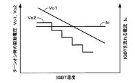
- FIG. 2 is a diagram showing a turn-on drive voltage characteristic of the insulated gate semiconductor device.
- FIG. 1 shows a schematic configuration of the driving device 3a on behalf of one of the driving devices 3a to 3n that respectively drive the plurality of IGBTs 2a to 2n shown in FIG. 3b to 3n are similarly configured. Further, the same reference numerals are given to the same elements as those constituting the driving device 3a shown in FIG.
- the driving device 3a includes a constant current source 8 and a current mirror circuit 9, and the constant current source 8 and the current mirror circuit 9 constitute the constant current circuit 5 shown in FIG.
- the drive device 3a also includes a discharge circuit 6, a switching circuit 7, a voltage control circuit 10, and a constant current circuit 11.
- the IGBT 2a incorporates a temperature detection diode 12 that detects heat generated by the IGBT 2a as a temperature detection element.
- the constant current source 8 includes an operational amplifier 8a, an n-channel FET (hereinafter abbreviated as n-FET) 8b, and a resistor 8c.
- the operational amplifier 8a is supplied with the reference voltage Vref at its non-inverting input terminal (+), and the output terminal is connected to the gate of the n-FET 8b.
- the source of the n-FET 8b is connected to the inverting input terminal ( ⁇ ) of the operational amplifier 8a and to the ground line GND through the resistor 8c.
- the current mirror circuit 9 includes a pair of p-channel FETs (hereinafter abbreviated as p-FETs) 9a and 9b.
- the p-FET 9a has a source connected to the power supply line, a drain connected to its own gate, and an output of the constant current source 8 (ie, the drain of the n-FET 8b).
- the p-FET 9b has a source connected to the power supply line, a drain connected to the gate of the IGBT 2a, and a gate connected to the drain and gate of the p-FET 9a.
- the current mirror circuit 9 when the p-FET 9a is driven by a constant current Io output from the constant current source 8, the p-FET 9b has a constant current [k ⁇ Io (k is Constant)] is output. As a result, the current mirror circuit 9 supplies a constant current [k ⁇ Io] proportional to the current Io to the gate of the IGBT 2a.
- the discharge circuit 6 includes a buffer circuit 6a and an n-FET 6b.
- a drive signal is input to its input terminal, and the gate of the n-FET 6b is connected to its output terminal.
- the n-FET 6b has a drain connected to the gate of the IGBT 2a and a source connected to the ground line GND.
- the buffer circuit 6a when the drive signal input to the buffer circuit 6a is [H level], the buffer circuit 6a turns on the n-FET 6b to discharge the charge accumulated in the gate of the IGBT 2a to the ground line GND. This turns off the IGBT 2a.
- the switching circuit 7 includes a p-FET 7a and a level shift circuit 7b.
- the p-FET 7 a has a source connected to the power supply line and a drain connected to the gate of the p-FET 9 b of the current mirror circuit 9.
- a drive signal is input to the input, and the gate of the p-FET 7a is connected to the output.
- the switching circuit 7 turns on / off the p-FETs 9a and 9b of the current mirror circuit 9 by the level shift circuit 7b controlling the gate voltage of the p-FET 7a by level-shifting the drive signal.
- the level shift circuit 7b turns off the p-FET 7a and turns on the current mirror circuit 9.
- the p-FET 9b of the current mirror circuit 9 supplies a constant current [k ⁇ Io] to the gate of the IGBT 2a.
- the drive signal of [L level] is supplied to the discharge circuit 6 and the n-FET 6b of the discharge circuit 6 is turned off, so that the IGBT 2a is turned on.
- the level shift circuit 7b turns on the p-FET 7a.
- the current mirror circuit 9 is turned off, and the current supply from the current mirror circuit 9 to the gate of the IGBT 2a is stopped.
- the discharge circuit 6 the n-FET 6b is turned on when the [H level] drive signal is input, the gate of the IGBT 2a is connected to the ground line GND, and the charge accumulated in the gate of the IGBT 2a is discharged. Is done. As a result, the IGBT 2a is turned off.
- the IGBT 2a has a built-in temperature detection diode 12.
- the temperature detecting diode 12 has an anode connected to the constant current circuit 11 and a cathode connected to the ground line GND.
- the temperature detection diode 12 is configured such that a constant current output from the constant current circuit 11 is constantly supplied, and a forward voltage that changes according to the temperature of the IGBT 2a is output as the diode voltage Vf.
- the temperature characteristic of the forward voltage of the temperature detecting diode 12 is, for example, about ⁇ 2.0 to ⁇ 2.5 mV / ° C.
- the voltage control circuit 10 includes an operational amplifier 10a and four resistors 10b, 10c, 10d, and 10e, and constitutes a differential amplifier circuit. That is, the operational amplifier 10a is configured such that the reference voltage Vref0 is supplied to the inverting input terminal ( ⁇ ) via the resistor 10b, and is connected to its own output via the resistor 10c. The reference voltage Vref0 is for prescribing the drive voltage Vo1 of the constant current source 8 and the current mirror circuit 9, and is set in advance.
- the non-inverting input terminal (+) of the operational amplifier 10a is configured to input the diode voltage Vf of the temperature detection diode 12 through the resistor 10d, and is connected to the ground line GND through the resistor 10e.
- the voltage control circuit 10 is configured to amplify the voltage difference ⁇ V between the diode voltage Vf and the reference voltage Vref0 and output the drive voltage Vo1 of the constant current source 8 and the current mirror circuit 9.
- the voltage control circuit 10 outputs when the values of the resistors 10b and 10d, which are input resistors of the operational amplifier 10a, are R1, and the values of the feedback resistor 10c and the ground resistor 10e are R2, respectively.
- the voltage Vo1 is feedback controlled.
- the temperature of the IGBT 2a increases (decreases) ⁇ the diode voltage Vf decreases (increases) ⁇ the drive voltage Vo1 decreases (increases) ⁇
- the final gate voltage when the IGBT 2a is turned on is determined by the drive voltage Vo1.
- the feedback that the gate voltage of the IGBT 2a is reduced (increased) ⁇ the current flowing through the IGBT 2a is reduced (increased) is performed.
- the driving for driving the gate of the IGBT 2a by controlling the driving voltage Vo1 of the constant current source 8 and the current mirror circuit 9 according to the variation of the gate threshold voltage caused by the individual difference of the IGBT 2a (according to the generated temperature). It is possible to control the magnitude of the voltage Vo1.
- the resistances 10b and 10d of the input resistance, the resistance 10c of the feedback resistance, and the resistance 10e of the ground resistance are the same in temperature characteristics, variations in their resistance values can be offset.
- the temperature characteristic of the reference voltage Vref0 is kept within ⁇ 3% of the standard value in the range of ⁇ 20 to 125 ° C., for example, and the temperature characteristic of the diode voltage Vf is ⁇ 10%. To keep it within%.
- the temperature characteristics of the driving voltage Vo1 of the constant current source 8 and the current mirror circuit 9 are sufficiently accurate with respect to the temperature change of the IGBTs 2a to 2n. can do.
- the magnitude of the drive voltage Vo1 for driving the gate is feedback controlled according to the temperature (diode voltage Vf) of the IGBTs 2a to 2n. And can be optimized. That is, as shown in FIG. 2, feedback control is performed so that the magnitude of the drive voltage Vo1 continuously decreases as the temperature of the IGBTs 2a to 2n increases (the diode voltage Vf decreases), and the IGBTs 2a to 2n The current Ic flowing through is kept constant.
- the temperature detection diode 12 including the temperature of the IGBT 2a detects and feedback-controls the driving voltage Vo1 of the constant current source 8 and the current mirror circuit 9. ing. Due to the constant current drive and drive voltage control of the IGBTs 2a to 2n, the currents Ic flowing through the individual IGBTs 2a to 2n converge to current values corresponding to the reference voltage Vref0 having substantially the same temperature characteristics, and all the IGBTs 2a to 2n The 2n current Ic can be equalized.
- FIG. 3 is a diagram showing a schematic configuration example of a main part of a drive device for an insulated gate semiconductor element according to the second embodiment.
- the same components as those shown in FIG. 1 are denoted by the same reference numerals, and detailed description thereof is omitted.
- the voltage control circuit 10 is replaced with a voltage control circuit 13 having a different configuration as compared with the first embodiment.
- the voltage control circuit 13 includes a plurality of (four in the illustrated example) comparators 13a, 13b, 13c, and 13d, p-FETs 13f, 13g, 13h, and 13i that function as switching elements, and resistors 13k, 13l, 13m, 13n, and 13o.
- the comparators 13a, 13b, 13c, and 13d are configured to input the diode voltage Vf of the temperature detection diode 12 to their inverting input terminals ( ⁇ ).
- the non-inverting input terminals (+) of the comparators 13a, 13b, 13c, and 13d receive the first threshold voltage Vref1, the second threshold voltage Vref2, the third threshold voltage Vref3, and the fourth threshold voltage Vref4, respectively. It is configured as follows.
- the outputs of the comparators 13a, 13b, 13c and 13d are connected to the gates of the p-FETs 13f, 13g, 13h and 13i, respectively.
- the source of the p-FET 13f is connected to the power supply voltage Vcc supplied as the device power supply voltage, and is connected to the ground line GND via resistors 13k, 13l, 13m, 13n, and 13o connected in series to form a voltage dividing circuit. It is connected.
- the connection point between the resistor 13k and the resistor 13l is connected to the source of the p-FET 13g
- the connection point between the resistor 13l and the resistor 13m is connected to the source of the p-FET 13h
- the connection point between the resistor 13m and the resistor 13n is ,
- P-FET 13i is connected to the source.
- the drains of the p-FETs 13f, 13g, 13h, and 13i are combined and output as a drive voltage Vo2 for the constant current source 8 and the current mirror circuit 9.
- the comparators 13a to 13d compare the diode voltage Vf with the first to fourth threshold voltages Vref1 to Vref4, respectively, and the constant current source 8 and the current mirror circuit 9 according to the comparison results.
- the drive voltage Vo2 is variably set. Normally (when the temperature of the IGBT 2a is equal to or lower than a predetermined temperature), the relationship between the diode voltage Vf and the first to fourth threshold voltages Vref1 to Vref4 is as follows. Vf>Vref1>Vref2>Vref3> Vref4 It is.
- the power supply voltage Vcc is divided by five resistors 13k (R11), 13l (R12), 13m (R13), 13n (R14), and 13o (R15) connected in series, and the divided voltage and power supply The voltage Vcc is selected according to the diode voltage Vf and output as the drive voltage Vo2.
- the diode voltage Vf is higher than the first threshold voltage Vref1, so that the p-FETs 13f to 13i are all turned on, and the drive voltage Vo2 becomes equal to the power supply voltage Vcc.
- the resistors 13l (R12), 13m (R13), and 13n (R14) are short-circuited by turning on the p-FETs 13g to 13i.
- the driving voltage Vo2 of the IGBT 2a is changed stepwise (here, five steps) according to the temperature of the IGBT, as shown in FIG. . Therefore, although the control accuracy is rougher than that of the first embodiment, the magnitude of the drive voltage Vo2 supplied to the gates of the IGBTs 2a to 2n is set to the turn-on of the IGBTs 2a to 2n, as in the first embodiment. Can be tailored to the characteristics. In addition, the currents Ic flowing through the IGBTs 2a to 2n can be kept constant, and the currents Ic flowing through the plurality of IGBTs 2a to 2n provided in parallel can be effectively prevented from becoming unbalanced. As a result, current concentration on a specific IGBT can be prevented, and thermal destruction can be prevented.
- this invention is not limited to each embodiment mentioned above.
- the configuration of the constant current source 8 is different, or switching of the driving voltage Vo2 in the insulated gate semiconductor device driving apparatus according to the second embodiment is performed in more or less stages depending on the diode voltage Vf.
- the present invention can also be applied to a case where a MOS-FET is driven instead of the IGBT described above.
- the reference voltages Vref and Vref0 and the first to fourth threshold voltages Vref1 to Vref4 included in the individual driving devices 3a to 3n are used as all the driving devices. It can also be configured to be shared by 3a to 3n.
- the present invention can be variously modified and implemented without departing from the scope of the invention.
Landscapes
- Engineering & Computer Science (AREA)
- Power Engineering (AREA)
- Power Conversion In General (AREA)
Abstract
並列接続された複数の絶縁ゲート型半導体素子をバランス良く並列駆動する。 並列接続された複数のIGBTの1つ(2a)をターンオン制御するとき、そのゲートを定電流源(8)とカレントミラー回路(9)とを含む定電流回路(5)によって定電流駆動しながら、電圧制御回路(10)がIGBT(2a)に内蔵された温度検出用ダイオード(12)により温度に対応する値で出力されるダイオード電圧(Vf)と基準電圧(Vref0)との電圧差ΔVに応じた可変の電圧を、IGBT(2a)のゲートを駆動する駆動電圧(Vo1)として定電流源(8)とカレントミラー回路(9)に出力する。これにより、定電流駆動によりターンオン時における損失およびノイズを低減できることに加え、複数のIGBT(2a)の個体差に起因するゲート閾値電圧のばらつきに拘わることなく、そのターンオン時間および流れる電流の電流値を揃えることができる。
Description
本発明は絶縁ゲート型半導体素子の駆動装置および電力変換装置に関し、特に並列接続された複数の絶縁ゲート型半導体素子をそれぞれ一定の電流で均等に並列駆動することのできる絶縁ゲート型半導体素子の駆動装置および電力変換装置に関する。
電力変換装置では、負荷を制御する半導体素子として電力制御用のIGBT(Insulated-Gate Bipolar Transistors)、MOS-FET(Metal-Oxide-Semiconductor Field-Effect Transistor)等の絶縁ゲート型半導体素子が使用されている。特に、大電力負荷に対応した電力変換装置では、絶縁ゲート型半導体素子を複数個並列に接続し、これらの絶縁ゲート型半導体素子を並列駆動することが一般に行われる。
図4は複数の絶縁ゲート型半導体素子の駆動装置を並列配置した電力変換装置の概略構成例を示す図である。
この構成例によれば、電力変換装置1は、複数のIGBT2a~2nと、これらIGBT2a~2nをそれぞれ個別に駆動する複数の駆動装置3a~3nとを備えている。複数のIGBT2a~2nは、各コレクタを相互に接続し、各エミッタを相互に接続することで並列に配置され、各ゲートは、対応する駆動装置3a~3nの出力にそれぞれ接続されている。これらのIGBT2a~2nは、相互に接続されたコレクタが大電力負荷4に接続され、相互に接続されたエミッタが接地ラインGNDに接続されている。
この構成例によれば、電力変換装置1は、複数のIGBT2a~2nと、これらIGBT2a~2nをそれぞれ個別に駆動する複数の駆動装置3a~3nとを備えている。複数のIGBT2a~2nは、各コレクタを相互に接続し、各エミッタを相互に接続することで並列に配置され、各ゲートは、対応する駆動装置3a~3nの出力にそれぞれ接続されている。これらのIGBT2a~2nは、相互に接続されたコレクタが大電力負荷4に接続され、相互に接続されたエミッタが接地ラインGNDに接続されている。
複数の駆動装置3a~3nは、共通の駆動信号をそれぞれ受けて、それぞれ対応するIGBT2a~2nを並列に駆動する。これにより、複数のIGBT2a~2nは、1つのパワースイッチングデバイスとして機能し、大電力負荷4を駆動する。
ここで、駆動装置3a~3nは、IGBT2a~2nのゲートに所定の電圧を印加することで制御している。これに対し、IGBT2a~2nのゲートに一定の電流を供給してIGBT2a~2nをターンオンさせることにより、ターンオン時における損失およびノイズの発生を低減することが提唱されている(例えば、特許文献1参照)。
図5は従来のIGBTのゲートに一定の電流を供給する方式による絶縁ゲート型半導体素子の駆動装置の概略構成を示す図である。なお、図4に示す電力変換装置1の複数の駆動装置3a~3nは、それぞれ同じ構成を有しているので、この図5では、代表して駆動装置3aの構成を例示している。
駆動装置3aは、一定電流を生成する定電流回路5と、IGBT2aのゲートを接地する放電回路6と、駆動信号に応じて定電流回路5と放電回路6とを相補的にオン・オフ制御する切替回路7とを備えている。
以上の構成の駆動装置3aによれば、切替回路7は、IGBT2aをターンオン制御する駆動信号を入力したとき、定電流回路5にて生成された一定電流をIGBT2aのゲートに供給してIGBT2aをターンオンする。一方、IGBT2aをターンオフ制御する駆動信号を入力したときには、切替回路7は、放電回路6を作動させ、IGBT2aのゲートを接地してゲートに蓄積された電荷を放電することにより、IGBT2aをターンオフする。
このように構成された駆動装置3aによれば、IGBT2aのゲートに一定電流を供給してIGBT2aをターンオンさせるので、IGBT2aのゲートに蓄積される電荷の充電速度を一定化することができる。したがって、IGBTのゲート電圧を制御してIGBTをオン・オフする従来一般的な駆動方法のように、IGBTのゲートを駆動する半導体素子(トランジスタ)の温度に依存するオン抵抗の変化に起因してIGBTのゲートの充電速度が変化することがない。故に、温度変化に拘わることなくIGBT2aのターンオン時間を一定化することができ、ターンオン時における損失とノイズを低減することが可能となる。
しかし、並列接続した複数のIGBT2a~2nにそれぞれ一定電流を供給してターンオンさせても、各IGBT2a~2nの個体差に伴うゲート閾値電圧のばらつきに起因してゲート閾値電圧の低いIGBTに電流が集中して流れる虞がある。このようなターンオン時における電流の集中は、IGBTの熱的破壊を招来する危険性がある。
そこで、従来では、あらかじめ複数のIGBT2a~2nのゲート電流値を測定して記憶しておき、これらのゲート電流値に基づいて各IGBT2a~2nのゲート電流を制御して電流バランスをとることが提唱されている(例えば、特許文献2参照)。
また、目標ゲート閾値電圧とIGBT2a~2nのゲート閾値電圧との差に応じてその駆動用制御電圧とIGBT2a~2nのエミッタ電圧とに等電位のオフセットを与えることも提唱されている(例えば、特許文献3参照)。これにより、IGBT2a~2nは、それぞれがターンオンするときのタイミングが揃えられ、複数のIGBT2a~2nにおいて電流バランスをとるようにしている。
また、低温素子、高温素子を検出し、高温素子にはより遅延を大きくした駆動信号を供給することで電流を流れにくくし、低温素子には遅延を小さくした駆動信号を供給することで電流を流れやすくすることも提唱されている(例えば、特許文献4参照)。
また、低温素子、高温素子を検出し、低温素子には遅延した駆動信号を供給してターンオフ時におけるスイッチング損失を増加させて発熱量を多くすることにより、高温素子との温度および電流を均等化することも提唱されている(例えば、特許文献5参照)。
さらに、並列接続された2つのパワーMOS-FETの温度を比較し、温度が高い方のパワーMOS-FETのゲート電圧を下げることにより、パワーMOS-FETの温度の均等化を図ることも提唱されている(例えば、特許文献6参照)。
しかしながら、特許文献2,3にそれぞれ示される手法においては、あらかじめ複数のIGBTのゲート電流値またはゲート閾値電圧をそれぞれ求めておく必要がある。しかも、あらかじめ求めたIGBTの特性データに従って各IGBTのゲート電流を個別に制御したり、各IGBTの駆動用制御電圧とエミッタ電圧とをそれぞれオフセット制御したりすることが必要であり、手間が掛かる上に構成が複雑化するという問題点があった。
また、特許文献4-6にそれぞれ示される手法においては、並列に接続された2つの半導体素子の温度を比較し、両者の温度バランスを取るようにしたものであるので、半導体素子が3つ以上並列接続されている場合には対応することができない。さらに、2つの半導体素子は、一方が他方の温度によって動作するので、ハンチング動作を起こす可能性がある。また、特許文献6に記載の装置では、ゲート電圧の変化量を一定にしているため、2つの半導体素子が温度平衡状態に達するまで、温度を下げる制御を交互に繰り返す必要があり、応答性が悪くなってしまう。
本発明はこのような事情を考慮してなされたもので、その目的は、並列接続された複数の絶縁ゲート型半導体素子を一定電流で均等に、かつ、電流バランス良く並列駆動することのできる簡易な構成の絶縁ゲート型半導体素子の駆動装置および電力変換装置を提供することにある。
本発明では上記の課題を解決するために、並列接続された複数の絶縁ゲート型半導体素子の1つを駆動する駆動装置が提供される。この絶縁ゲート型半導体素子の駆動装置は、絶縁ゲート型半導体素子のターンオン時にゲートに一定電流を供給する定電流回路を備え、絶縁ゲート型半導体素子を定電流駆動する。駆動装置は、また、絶縁ゲート型半導体素子のターンオフ時にゲートに蓄積された電荷を放電する放電回路と、駆動信号が入力され、絶縁ゲート型半導体素子に対して定電流回路で定電流駆動を行うか放電回路で電荷の放電を行うかの切り替えを行う切替回路とを備えている。本発明の駆動装置は、さらに、電圧制御回路を備え、絶縁ゲート型半導体素子が内蔵する温度検出素子が検出した温度に応じて定電流回路の電源電圧を可変制御するようにしている。すなわち、この駆動装置は、絶縁ゲート型半導体素子を定電流駆動と駆動電圧制御とを併用したことにより、複数の絶縁ゲート型半導体素子を流れる電流を均等化している。
また、本発明では、並列接続された複数の絶縁ゲート型半導体素子と、絶縁ゲート型半導体素子をそれぞれ駆動する複数の駆動装置とを備えた電力変換装置が提供される。ここで、すべての駆動装置は、定電流回路を備え、絶縁ゲート型半導体素子のターンオン時にゲートに一定電流を供給するようにしている。また、すべての駆動装置は、絶縁ゲート型半導体素子のターンオフ時にゲートに蓄積された電荷を放電する放電回路と、駆動信号が入力され、絶縁ゲート型半導体素子に対して定電流回路で定電流駆動を行うか放電回路で電荷の放電を行うかの切り替えを行う切替回路とを備えている。本発明の駆動装置は、さらに、電圧制御回路を備え、絶縁ゲート型半導体素子が内蔵する温度検出素子が検出した温度に対応する検出電圧と基準電圧との差に応じて定電流回路の電源電圧を可変制御するようにしている。すなわち、この電力変換装置では、すべての駆動装置は、絶縁ゲート型半導体素子を定電流駆動と駆動電圧制御とを併用したことにより、複数の絶縁ゲート型半導体素子を流れる電流を均等化している。
上記構成の絶縁ゲート型半導体素子の駆動装置および電力変換装置は、温度検出素子が検出した温度に応じて各絶縁ゲート型半導体素子をそれぞれターンオンする為の駆動電圧の大きさが調整されることで、複数の絶縁ゲート型半導体素子の個体差に起因するゲート閾値電圧のばらつきに拘わることなく、そのターンオン時間を揃えることができる。
しかも、絶縁ゲート型半導体素子のゲートには一定電流を供給するので、温度に依存する絶縁ゲート型半導体素子のゲートを駆動する半導体素子(トランジスタ)のオン抵抗の変化に影響されることなく各絶縁ゲート型半導体素子をターンオンさせることができ、ターンオン時における損失とノイズを低減することができる。
したがって、絶縁ゲート型半導体素子に内蔵される温度検出素子から発生する電圧に応じてその絶縁ゲート型半導体素子のゲートに供給する駆動電圧の大きさを調整するという簡易な構成の下で、複数の絶縁ゲート型半導体素子の電流バランスを確保することができ、電流集中による絶縁ゲート型半導体素子の熱的破壊を未然に防止することができる等の実用上多大なる効果が奏せられる。
本発明の上記および他の目的、特徴および利点は本発明の例として好ましい実施の形態を表す添付の図面と関連した以下の説明により明らかになるであろう。
以下、本発明の実施の形態について、絶縁ゲート型半導体素子としてIGBTを使用した場合を例に図面を参照して詳細に説明する。
図1は第1の実施の形態に係る絶縁ゲート型半導体素子の駆動装置の要部概略構成例を示す図、図2は絶縁ゲート型半導体素子のターンオン駆動電圧特性を示す図である。なお、図1は、図4に記した複数のIGBT2a~2nをそれぞれ駆動する駆動装置3a~3nの中の1つを代表して駆動装置3aの概略構成を示しているが、他の駆動装置3b~3nも同様に構成される。また、図5に示した駆動装置3aを構成する要素と同一の要素には同一の符号を付してある。
図1は第1の実施の形態に係る絶縁ゲート型半導体素子の駆動装置の要部概略構成例を示す図、図2は絶縁ゲート型半導体素子のターンオン駆動電圧特性を示す図である。なお、図1は、図4に記した複数のIGBT2a~2nをそれぞれ駆動する駆動装置3a~3nの中の1つを代表して駆動装置3aの概略構成を示しているが、他の駆動装置3b~3nも同様に構成される。また、図5に示した駆動装置3aを構成する要素と同一の要素には同一の符号を付してある。
駆動装置3aは、定電流源8とカレントミラー回路9とを備え、定電流源8およびカレントミラー回路9は、図5に示した定電流回路5を構成している。駆動装置3aは、また、放電回路6と、切替回路7と、電圧制御回路10と、定電流回路11とを備えている。また、IGBT2aには、温度検出素子として、IGBT2aが発生する熱を検出する温度検出用ダイオード12が内蔵されている。
定電流源8は、オペアンプ8aと、nチャネル型のFET(以下、n-FETと略記する)8bと、抵抗8cとを備えている。オペアンプ8aは、その非反転入力端子(+)に基準電圧Vrefが供給され、出力端子は、n-FET8bのゲートに接続されている。n-FET8bのソースは、オペアンプ8aの反転入力端子(-)に接続されるとともに、抵抗8cを介して接地ラインGNDに接続されている。
この定電流源8においては、オペアンプ8aの2つの入力端子が仮想短絡することにより、n-FET8bのソースと接地ラインとの間に介挿された抵抗8cに基準電圧Vrefが印加される。したがって、この定電流源8の出力電流(すなわち、n-FET8bのドレイン電流)Ioは、抵抗8cの値をRrefとしたとき、Io=Vref/Rrefとして一定化される。
カレントミラー回路9は、1対のpチャネル型のFET(以下、p-FETと略記する)9a,9bを備えている。p-FET9aは、ソースが電源ラインに接続され、ドレインが自身のゲートに接続されているとともに、定電流源8の出力(すなわち、n-FET8bのドレイン)に接続されている。一方、p-FET9bは、ソースが電源ラインに接続され、ドレインがIGBT2aのゲートに接続され、ゲートがp-FET9aのドレインおよびゲートに接続されている。
このカレントミラー回路9は、p-FET9aが定電流源8によって出力される一定の電流Ioにより駆動されると、p-FET9bが一定の電流Ioに比例した一定の電流[k・Io(kは定数)]を出力する。これにより、カレントミラー回路9は、電流Ioに比例した一定の電流[k・Io]をIGBT2aのゲートに供給することになる。
放電回路6は、バッファ回路6aとn-FET6bとを備えている。バッファ回路6aは、その入力端子に駆動信号が入力され、出力端子には、n-FET6bのゲートが接続されている。n-FET6bは、ドレインがIGBT2aのゲートに接続され、ソースが接地ラインGNDに接続されている。
この放電回路6は、バッファ回路6aに入力される駆動信号が[Hレベル]のときに、バッファ回路6aがn-FET6bをオンしてIGBT2aのゲートに蓄積された電荷を接地ラインGNDに放電し、これによってIGBT2aをターンオフする。
切替回路7は、p-FET7aとレベルシフト回路7bとを備えている。p-FET7aは、ソースが電源ラインに接続され、ドレインがカレントミラー回路9のp-FET9bのゲートに接続されている。レベルシフト回路7bは、その入力に駆動信号が入力され、出力には、p-FET7aのゲートが接続されている。
この切替回路7は、レベルシフト回路7bが駆動信号をレベルシフトしてp-FET7aのゲート電圧を制御することによりカレントミラー回路9のp-FET9a,9bをオン・オフする。
すなわち、切替回路7は、駆動信号が[Lレベル]のとき、レベルシフト回路7bがp-FET7aをオフし、カレントミラー回路9をオンにする。これにより、カレントミラー回路9のp-FET9bは、IGBT2aのゲートに一定の電流[k・Io]を供給する。このとき、[Lレベル]の駆動信号が放電回路6に供給されて、放電回路6のn-FET6bがオフされているので、IGBT2aは、ターンオンされる。
一方、[Hレベル]の駆動信号が入力されているとき、切替回路7は、レベルシフト回路7bがp-FET7aをオンする。これにより、カレントミラー回路9は、オフされ、カレントミラー回路9からIGBT2aのゲートへの電流供給が停止される。このとき、放電回路6は、[Hレベル]の駆動信号が入力されていることによりn-FET6bがオンし、IGBT2aのゲートが接地ラインGNDに接続されてIGBT2aのゲートに蓄積された電荷が放電される。これによってIGBT2aは、ターンオフされる。
IGBT2aは、温度検出用ダイオード12を内蔵している。その温度検出用ダイオード12は、アノードに定電流回路11が接続され、カソードは、接地ラインGNDに接続されている。温度検出用ダイオード12は、定電流回路11から出力される定電流が常時流されていて、IGBT2aの温度により変化する順方向電圧をダイオード電圧Vfとして出力するように構成されている。なお、温度検出用ダイオード12の順方向電圧の温度特性は、例えば、-2.0~-2.5mV/℃程度である。
電圧制御回路10は、オペアンプ10aと、4つの抵抗10b,10c,10d,10eとを備え、差動増幅回路を構成している。すなわち、オペアンプ10aは、その反転入力端子(-)に抵抗10bを介して基準電圧Vref0が供給されるように構成されるとともに、抵抗10cを介して自身の出力に接続されている。基準電圧Vref0は、定電流源8およびカレントミラー回路9の駆動電圧Vo1を規定するためのもので、あらかじめ設定されている。オペアンプ10aの非反転入力端子(+)は、抵抗10dを介して温度検出用ダイオード12のダイオード電圧Vfを入力するように構成されるとともに、抵抗10eを介して接地ラインGNDに接続されている。
電圧制御回路10は、ダイオード電圧Vfと基準電圧Vref0との電圧差ΔVを増幅し、定電流源8およびカレントミラー回路9の駆動電圧Vo1を出力するように構成されている。
具体的には、オペアンプ10aの入力抵抗である抵抗10b,10dの値をそれぞれR1とし、帰還抵抗の抵抗10cおよび接地抵抗の抵抗10eの値をそれぞれR2としたとき、電圧制御回路10が出力する駆動電圧Vo1は、
Vo1=(R2/R1)・(Vf-Vref0)
となる。すなわち、電圧制御回路10は、IGBT2aで発生する熱を内蔵する温度検出用ダイオード12が検出してダイオード電圧Vfを出力し、そのダイオード電圧Vfに応じて定電流源8およびカレントミラー回路9の駆動電圧Vo1をフィードバック制御している。具体的には、IGBT2aの温度が上がる(下がる)→ダイオード電圧Vfが小さく(大きく)なる→駆動電圧Vo1が小さくなる(大きくなる)→IGBT2aのオン時の最終ゲート電圧は駆動電圧Vo1で決まるので、IGBT2aのゲート電圧が小さくなる(大きくなる)→IGBT2aに流れる電流が小さくなる(大きくなる)、というフィードバックが行われる。
Vo1=(R2/R1)・(Vf-Vref0)
となる。すなわち、電圧制御回路10は、IGBT2aで発生する熱を内蔵する温度検出用ダイオード12が検出してダイオード電圧Vfを出力し、そのダイオード電圧Vfに応じて定電流源8およびカレントミラー回路9の駆動電圧Vo1をフィードバック制御している。具体的には、IGBT2aの温度が上がる(下がる)→ダイオード電圧Vfが小さく(大きく)なる→駆動電圧Vo1が小さくなる(大きくなる)→IGBT2aのオン時の最終ゲート電圧は駆動電圧Vo1で決まるので、IGBT2aのゲート電圧が小さくなる(大きくなる)→IGBT2aに流れる電流が小さくなる(大きくなる)、というフィードバックが行われる。
すなわち、IGBT2aの個体差に起因するゲート閾値電圧のばらつきに応じて(生じる温度に応じて)定電流源8およびカレントミラー回路9の駆動電圧Vo1を制御することにより、IGBT2aのゲートを駆動する駆動電圧Vo1の大きさを制御することが可能となる。
特に、入力抵抗の抵抗10b,10d、帰還抵抗の抵抗10cおよび接地抵抗の抵抗10eは、温度特性が同じものを用いているので、それらの抵抗値のばらつきを相殺することができる。さらには、すべての駆動装置3a~3nにおいて、基準電圧Vref0の温度特性を、例えば、-20~125℃の範囲で標準値の±3%以内に収めるとともに、ダイオード電圧Vfの温度特性を±10%以内に収めるようにしている。これにより、上述した抵抗値のばらつきの相殺効果と相俟って、定電流源8およびカレントミラー回路9の駆動電圧Vo1の温度特性は、IGBT2a~2nの温度変化に対して十分に精度を高くすることができる。
この結果、並列接続された複数のIGBT2a~2nのゲート閾値電圧にばらつきがあっても、IGBT2a~2nの温度(ダイオード電圧Vf)に応じ、ゲートを駆動する駆動電圧Vo1の大きさを、フィードバック制御して最適化することができる。すなわち、図2に示したように、IGBT2a~2nの温度の温度が高くなる(ダイオード電圧Vfが小さくなる)に従って駆動電圧Vo1の大きさが連続的に小さくなるようにフィードバック制御し、IGBT2a~2nに流れる電流Icを一定に保つようにしている。これにより、IGBT2a~2nの中に、ゲート閾値電圧のばらつきに起因して流れる電流が変化し、温度が変化するものがあったとしても、駆動電圧Vo1が変化することで、流れる電流Icが一定に保たれるようになる。このため、並列に設けられた複数のIGBT2a~2nのそれぞれに流れる電流Icがアンバランスとなることを効果的に防ぐことが可能となり、特定のIGBTへの電流集中を防いでその熱的破壊を未然に防ぐことが可能となる。
このように、第1の実施形態に係る駆動装置3aによれば、IGBT2aの温度を内蔵する温度検出用ダイオード12が検出して定電流源8およびカレントミラー回路9の駆動電圧Vo1をフィードバック制御している。IGBT2a~2nの定電流駆動と駆動電圧制御とにより、個々のIGBT2a~2nに流れる電流Icは、温度特性がほぼ同じ基準電圧Vref0に対応する電流値にそれぞれ収束するようになり、すべてのIGBT2a~2nの電流Icを均等化できる。
図3は第2の実施の形態に係る絶縁ゲート型半導体素子の駆動装置の要部概略構成例を示す図である。この図3において、図1に示した構成要素と同じ構成要素については同じ符号を付して詳細な説明を省略する。
この第2の実施の形態に係る絶縁ゲート型半導体素子の駆動装置3aは、第1の実施の形態のものと比較して電圧制御回路10が別構成の電圧制御回路13によって置き換えられている。
すなわち、電圧制御回路13は、複数(図示の例では4個)の比較器13a,13b,13c,13dと、スイッチ素子として機能するp-FET13f,13g,13h,13iと、抵抗13k,13l,13m,13n,13oとを備えている。
比較器13a,13b,13c,13dは、それらの反転入力端子(-)に温度検出用ダイオード12のダイオード電圧Vfを入力するように構成されている。比較器13a,13b,13c,13dの非反転入力端子(+)は、第1の閾値電圧Vref1、第2の閾値電圧Vref2、第3の閾値電圧Vref3および第4の閾値電圧Vref4がそれぞれ入力するように構成されている。比較器13a,13b,13c,13dの出力は、p-FET13f,13g,13h,13iのゲートにそれぞれ接続されている。
p-FET13fのソースは、装置電源電圧として供給された電源電圧Vccに接続されるとともに、直列接続されて分圧回路を構成する抵抗13k,13l,13m,13n,13oを介して接地ラインGNDに接続されている。抵抗13kと抵抗13lとの接続点は、p-FET13gのソースに接続され、抵抗13lと抵抗13mとの接続点は、p-FET13hのソースに接続され、抵抗13mと抵抗13nとの接続点は、p-FET13iのソースに接続されている。そして、p-FET13f,13g,13h,13iのドレインは、纏められて定電流源8およびカレントミラー回路9の駆動電圧Vo2として出力するように構成されている。
電圧制御回路13によれば、比較器13a~13dがダイオード電圧Vfを第1~第4の閾値電圧Vref1~Vref4とそれぞれ比較し、これらの比較結果に応じて定電流源8およびカレントミラー回路9の駆動電圧Vo2を可変設定するようにしている。なお、通常(IGBT2aの温度が所定温度以下のとき)は、ダイオード電圧Vfとこれら第1~第4の閾値電圧Vref1~Vref4との関係は、
Vf>Vref1>Vref2>Vref3>Vref4
である。
Vf>Vref1>Vref2>Vref3>Vref4
である。
具体的には、電源電圧Vccを、直列接続した5つの抵抗13k(R11),13l(R12),13m(R13),13n(R14),13o(R15)で分圧し、分圧した電圧と電源電圧Vccとをダイオード電圧Vfに応じて選択し、駆動電圧Vo2として出力している。
例えば、通常動作の場合、ダイオード電圧Vfは、第1の閾値電圧Vref1より大きいので、p-FET13f~13iは、すべてオンした状態になり、駆動電圧Vo2は、電源電圧Vccと等しくなる。また、IGBT2aの温度が上昇し、ダイオード電圧Vfが第1の閾値電圧Vref1より低くなると、p-EET13fがオフとなるため、駆動電圧Vo2は、電源電圧Vccの分圧値となり、
Vo2=Vcc×R15/(R11+R15)
となる。このとき、抵抗13l(R12),13m(R13),13n(R14)は、p-FET13g~13iがオンしていることによって短絡されている。
Vo2=Vcc×R15/(R11+R15)
となる。このとき、抵抗13l(R12),13m(R13),13n(R14)は、p-FET13g~13iがオンしていることによって短絡されている。
IGBT2aの温度がさらに上昇して、ダイオード電圧Vfが第2の閾値電圧Vref2より低くなると、駆動電圧Vo2は、
Vo2=Vcc×R15/(R11+R12+R15)
となる。
Vo2=Vcc×R15/(R11+R12+R15)
となる。
このような電圧制御回路13を備える駆動装置3aによれば、IGBT2aの駆動電圧Vo2は、図2に示すように、IGBTの温度に応じて段階的(ここでは、5段階)に変化させている。したがって、第1の実施形態のものと比較してその制御精度が粗いものの、第1の実施形態と同様にIGBT2a~2nの各ゲートに供給する駆動電圧Vo2の大きさを、IGBT2a~2nのターンオン特性に合わせることができる。しかも、IGBT2a~2nにそれぞれ流れる電流Icを一定に保つことができ、並列に設けられた複数のIGBT2a~2nにそれぞれ流れる電流Icがアンバランスとなることを効果的に防ぐことが可能となる。この結果、特定のIGBTへの電流集中が防止され、その熱的破壊を未然に防ぐことが可能となる。
なお、本発明は上述した各実施形態に限定されるものではない。例えば、定電流源8の構成を別のものとしたり、第2の実施の形態に係る絶縁ゲート型半導体素子の駆動装置における駆動電圧Vo2の切り替えをダイオード電圧Vfに応じてさらに多段階もしくは少ない段階に可変設定したりすることも勿論可能である。また、前述したIGBTに代えてMOS-FETを駆動する場合にも、本発明を同様に適用可能なことも言うまでもない。さらに、駆動装置3a~3n間のばらつきを低減するために、個々の駆動装置3a~3nが備えていた基準電圧Vref,Vref0および第1~第4の閾値電圧Vref1~Vref4を、すべての駆動装置3a~3nで共用するように構成することもできる。その他、本発明はその要旨を逸脱しない範囲で種々変形して実施することができる。
上記については単に本発明の原理を示すものである。さらに、多数の変形、変更が当業者にとって可能であり、本発明は上記に示し、説明した正確な構成および応用例に限定されるものではなく、対応するすべての変形例および均等物は、添付の請求項およびその均等物による本発明の範囲とみなされる。
1 電力変換装置
2a~2n IGBT(絶縁ゲート型半導体素子)
3a~3n 駆動装置
4 大電力負荷
5 定電流回路
6 放電回路
6a バッファ回路
6b n-FET
7 切替回路
7a p-FET
7b レベルシフト回路
8 定電流源
8a オペアンプ
8b n-FET
8c 抵抗
9 カレントミラー回路
9a,9b p-FET
10 電圧制御回路
10a オペアンプ
10b,10c,10d,10e 抵抗
11 定電流回路
12 温度検出用ダイオード(温度検出素子)
13 電圧制御回路
13a,13b,13c,13d 比較器
13f,13g,13h,13i p-FET(スイッチ素子)
13k,13l,13m,13n,13o 抵抗
2a~2n IGBT(絶縁ゲート型半導体素子)
3a~3n 駆動装置
4 大電力負荷
5 定電流回路
6 放電回路
6a バッファ回路
6b n-FET
7 切替回路
7a p-FET
7b レベルシフト回路
8 定電流源
8a オペアンプ
8b n-FET
8c 抵抗
9 カレントミラー回路
9a,9b p-FET
10 電圧制御回路
10a オペアンプ
10b,10c,10d,10e 抵抗
11 定電流回路
12 温度検出用ダイオード(温度検出素子)
13 電圧制御回路
13a,13b,13c,13d 比較器
13f,13g,13h,13i p-FET(スイッチ素子)
13k,13l,13m,13n,13o 抵抗
Claims (8)
- 並列接続された複数の絶縁ゲート型半導体素子の1つを駆動する駆動装置において、
前記絶縁ゲート型半導体素子のターンオン時にゲートに一定電流を供給する定電流回路と、
前記絶縁ゲート型半導体素子のターンオフ時に前記ゲートに蓄積された電荷を放電する放電回路と、
駆動信号が入力され、前記絶縁ゲート型半導体素子に対して前記定電流回路で定電流駆動を行うか前記放電回路で前記電荷の放電を行うかの切り替えを行う切替回路と、
前記絶縁ゲート型半導体素子が内蔵する温度検出素子が検出した温度に応じて前記定電流回路の電源電圧を可変制御する電圧制御回路と、
を備えていることを特徴とする絶縁ゲート型半導体素子の駆動装置。 - 前記電圧制御回路は、前記温度検出素子によって検出された温度に対応する電圧とあらかじめ設定された基準電圧とを入力して温度に対応する前記電圧と前記基準電圧との電圧差を増幅した電圧を前記定電流回路の電源電圧として出力するオペアンプを備え、前記温度検出素子により検出された前記電圧に応じて前記定電流回路の前記電源電圧を連続的に変化させることを特徴とする請求項1記載の絶縁ゲート型半導体素子の駆動装置。
- 前記電圧制御回路は、前記温度検出素子によって検出された温度に対応する電圧とあらかじめ設定された複数の基準電圧とを比較する複数の比較器と、供給された装置電源電圧を分圧した複数の電圧出力を有する分圧回路と、前記装置電源電圧および複数の前記電圧出力と前記定電流回路の電源ラインとの間にそれぞれ接続され前記比較器の比較結果に応じてオン・オフ制御される複数のスイッチ素子とを備え、前記温度検出素子により検出された前記電圧に応じて複数の前記スイッチ素子を選択的にオン・オフさせることにより前記定電流回路の前記電源電圧を段階的に変化させることを特徴とする請求項1記載の絶縁ゲート型半導体素子の駆動装置。
- 前記定電流回路は、ソースが抵抗を介して接地ラインに接続された第1トランジスタと、前記抵抗の端子電圧と基準電圧とを比較して前記第1トランジスタのゲートを駆動するオペアンプと、ドレインおよびゲートが前記第1トランジスタのドレインに接続されソースが電源ラインに接続された第2のトランジスタと、ソースが前記電源ラインに接続されゲートが前記第2のトランジスタのゲートに接続されドレインが前記絶縁ゲート型半導体素子のゲートに接続された第3のトランジスタとを備えていることを特徴とする請求項1記載の絶縁ゲート型半導体素子の駆動装置。
- 前記放電回路は、前記切替回路から前記駆動信号を受けるバッファ回路と、ゲートが前記バッファ回路の出力端子に接続されソースが接地ラインに接続されドレインが前記絶縁ゲート型半導体素子のゲートに接続されたトランジスタ備えていることを特徴とする請求項1記載の絶縁ゲート型半導体素子の駆動装置。
- 前記切替回路は、ソースが前記定電流回路の前記電源ラインに接続されドレインが前記第2のトランジスタのゲートに接続された第4のトランジスタと、前記駆動信号をレベルシフトして前記第4のトランジスタのゲートに供給するレベルシフト回路とを備えていることを特徴とする請求項4記載の絶縁ゲート型半導体素子の駆動装置。
- 並列接続された複数の絶縁ゲート型半導体素子と、前記絶縁ゲート型半導体素子をそれぞれ駆動する複数の駆動装置とを備えた電力変換装置において、
前記駆動装置は、
前記絶縁ゲート型半導体素子のターンオン時にゲートに一定電流を供給する定電流回路と、
前記絶縁ゲート型半導体素子のターンオフ時に前記ゲートに蓄積された電荷を放電する放電回路と、
駆動信号が入力され、前記絶縁ゲート型半導体素子に対して前記定電流回路で定電流駆動を行うか前記放電回路で前記電荷の放電を行うかの切り替えを行う切替回路と、
前記絶縁ゲート型半導体素子が内蔵する温度検出素子が検出した温度に対応する検出電圧と基準電圧との差に応じて前記定電流回路の電源電圧を可変制御する電圧制御回路と、
を備えていることを特徴とする電力変換装置。 - すべての前記駆動装置において、前記基準電圧の温度特性を-20~125℃の範囲で標準値の±3%以内とし、前記温度検出素子の温度特性を±10%以内としたことを特徴とする請求項7記載の電力変換装置。
Priority Applications (2)
| Application Number | Priority Date | Filing Date | Title |
|---|---|---|---|
| EP14820700.4A EP2958220B1 (en) | 2013-07-03 | 2014-05-30 | Drive device for insulated-gate semiconductor element, and power conversion device |
| US14/854,006 US9608622B2 (en) | 2013-07-03 | 2015-09-14 | Drive device for insulated-gate semiconductor element, and power converter |
Applications Claiming Priority (2)
| Application Number | Priority Date | Filing Date | Title |
|---|---|---|---|
| JP2013-139828 | 2013-07-03 | ||
| JP2013139828A JP6286899B2 (ja) | 2013-07-03 | 2013-07-03 | 絶縁ゲート型半導体素子の駆動装置および電力変換装置 |
Related Child Applications (1)
| Application Number | Title | Priority Date | Filing Date |
|---|---|---|---|
| US14/854,006 Continuation US9608622B2 (en) | 2013-07-03 | 2015-09-14 | Drive device for insulated-gate semiconductor element, and power converter |
Publications (1)
| Publication Number | Publication Date |
|---|---|
| WO2015001883A1 true WO2015001883A1 (ja) | 2015-01-08 |
Family
ID=52143473
Family Applications (1)
| Application Number | Title | Priority Date | Filing Date |
|---|---|---|---|
| PCT/JP2014/064482 Ceased WO2015001883A1 (ja) | 2013-07-03 | 2014-05-30 | 絶縁ゲート型半導体素子の駆動装置および電力変換装置 |
Country Status (4)
| Country | Link |
|---|---|
| US (1) | US9608622B2 (ja) |
| EP (1) | EP2958220B1 (ja) |
| JP (1) | JP6286899B2 (ja) |
| WO (1) | WO2015001883A1 (ja) |
Families Citing this family (10)
| Publication number | Priority date | Publication date | Assignee | Title |
|---|---|---|---|---|
| WO2018042873A1 (ja) * | 2016-08-29 | 2018-03-08 | 富士電機株式会社 | 絶縁ゲート型半導体素子の駆動回路 |
| WO2018150737A1 (ja) * | 2017-02-17 | 2018-08-23 | 富士電機株式会社 | 絶縁ゲート型半導体デバイス駆動回路 |
| JP2018186400A (ja) * | 2017-04-26 | 2018-11-22 | ラピスセミコンダクタ株式会社 | レベルシフト回路 |
| US10727745B2 (en) | 2017-07-25 | 2020-07-28 | Kinetic Technologies | Systems and methods for providing intelligent constant on-time control |
| JP6924277B2 (ja) * | 2017-12-22 | 2021-08-25 | 新電元工業株式会社 | パワーモジュール |
| TWI654515B (zh) * | 2018-05-16 | 2019-03-21 | 華邦電子股份有限公司 | 數位穩壓器 |
| CN110673679B (zh) * | 2018-07-03 | 2021-01-05 | 华邦电子股份有限公司 | 数字稳压器 |
| TWI716980B (zh) * | 2018-08-28 | 2021-01-21 | 美商高效電源轉換公司 | 使用具回授之主動前置驅動器的GaN驅動器 |
| CN115766908B (zh) * | 2021-09-02 | 2024-07-26 | 中车株洲电力机车研究所有限公司 | 通信协议信号并联接口电路和高压变频器 |
| FR3156990A1 (fr) * | 2023-12-13 | 2025-06-20 | Commissariat A L'energie Atomique Et Aux Energies Alternatives | Dispositif à branches parallèles |
Citations (12)
| Publication number | Priority date | Publication date | Assignee | Title |
|---|---|---|---|---|
| JPH0235015A (ja) | 1988-02-03 | 1990-02-05 | Iseki & Co Ltd | 歩行型モアのコレクタ開閉装置 |
| JPH08186976A (ja) * | 1994-12-29 | 1996-07-16 | Hitachi Ltd | パワー半導体素子の駆動装置 |
| JPH1042548A (ja) * | 1996-07-17 | 1998-02-13 | Fuji Electric Co Ltd | 半導体電力変換装置 |
| WO2001089090A1 (en) * | 2000-05-18 | 2001-11-22 | Mitsubishi Denki Kabushiki Kaisha | Power semiconductor device |
| JP2002142445A (ja) * | 2000-11-07 | 2002-05-17 | Toshiba Corp | 電力変換装置 |
| JP2002142492A (ja) | 2000-11-02 | 2002-05-17 | Denso Corp | 負荷制御装置 |
| JP2002369497A (ja) * | 2001-06-05 | 2002-12-20 | Fuji Electric Co Ltd | Ipm回路 |
| JP2008103895A (ja) | 2006-10-18 | 2008-05-01 | Fuji Electric Device Technology Co Ltd | 絶縁ゲート型デバイスの駆動回路 |
| JP2008178248A (ja) | 2007-01-19 | 2008-07-31 | Mitsubishi Electric Corp | 電力用半導体素子の駆動回路および電力変換装置 |
| JP2009135626A (ja) | 2007-11-29 | 2009-06-18 | Mitsubishi Electric Corp | 並列駆動装置 |
| JP2009159662A (ja) | 2007-12-25 | 2009-07-16 | Fuji Electric Systems Co Ltd | 電力用半導体素子の制御回路 |
| WO2014069146A1 (ja) * | 2012-11-01 | 2014-05-08 | 富士電機株式会社 | 絶縁ゲート型半導体素子の駆動装置 |
Family Cites Families (8)
| Publication number | Priority date | Publication date | Assignee | Title |
|---|---|---|---|---|
| JPH11235015A (ja) | 1998-02-13 | 1999-08-27 | Toshiba Corp | 電圧駆動型電力用半導体装置およびそのゲート制御方法 |
| KR20060060018A (ko) * | 2003-08-12 | 2006-06-02 | 코닌클리즈케 필립스 일렉트로닉스 엔.브이. | 전자 회로, 제 1 및 제 2 mosfet의 동작 방법 |
| US7521985B2 (en) * | 2005-07-01 | 2009-04-21 | Semiconductor Components Industries, L.L.C. | Method for regulating temperature and circuit therefor |
| JP5360002B2 (ja) * | 2010-06-28 | 2013-12-04 | 富士電機株式会社 | 半導体素子の駆動装置 |
| WO2012153458A1 (ja) * | 2011-05-11 | 2012-11-15 | 富士電機株式会社 | 制御装置 |
| ITMI20112278A1 (it) * | 2011-12-15 | 2013-06-16 | St Microelectronics Srl | Struttura bipolare di potenza, in particolare per applicazioni ad alta tensione |
| JP5942083B2 (ja) * | 2011-12-15 | 2016-06-29 | パナソニックIpマネジメント株式会社 | キャパシタ装置 |
| JP6045611B2 (ja) * | 2013-02-08 | 2016-12-14 | 三菱電機株式会社 | ゲート駆動回路 |
-
2013
- 2013-07-03 JP JP2013139828A patent/JP6286899B2/ja active Active
-
2014
- 2014-05-30 EP EP14820700.4A patent/EP2958220B1/en active Active
- 2014-05-30 WO PCT/JP2014/064482 patent/WO2015001883A1/ja not_active Ceased
-
2015
- 2015-09-14 US US14/854,006 patent/US9608622B2/en active Active
Patent Citations (12)
| Publication number | Priority date | Publication date | Assignee | Title |
|---|---|---|---|---|
| JPH0235015A (ja) | 1988-02-03 | 1990-02-05 | Iseki & Co Ltd | 歩行型モアのコレクタ開閉装置 |
| JPH08186976A (ja) * | 1994-12-29 | 1996-07-16 | Hitachi Ltd | パワー半導体素子の駆動装置 |
| JPH1042548A (ja) * | 1996-07-17 | 1998-02-13 | Fuji Electric Co Ltd | 半導体電力変換装置 |
| WO2001089090A1 (en) * | 2000-05-18 | 2001-11-22 | Mitsubishi Denki Kabushiki Kaisha | Power semiconductor device |
| JP2002142492A (ja) | 2000-11-02 | 2002-05-17 | Denso Corp | 負荷制御装置 |
| JP2002142445A (ja) * | 2000-11-07 | 2002-05-17 | Toshiba Corp | 電力変換装置 |
| JP2002369497A (ja) * | 2001-06-05 | 2002-12-20 | Fuji Electric Co Ltd | Ipm回路 |
| JP2008103895A (ja) | 2006-10-18 | 2008-05-01 | Fuji Electric Device Technology Co Ltd | 絶縁ゲート型デバイスの駆動回路 |
| JP2008178248A (ja) | 2007-01-19 | 2008-07-31 | Mitsubishi Electric Corp | 電力用半導体素子の駆動回路および電力変換装置 |
| JP2009135626A (ja) | 2007-11-29 | 2009-06-18 | Mitsubishi Electric Corp | 並列駆動装置 |
| JP2009159662A (ja) | 2007-12-25 | 2009-07-16 | Fuji Electric Systems Co Ltd | 電力用半導体素子の制御回路 |
| WO2014069146A1 (ja) * | 2012-11-01 | 2014-05-08 | 富士電機株式会社 | 絶縁ゲート型半導体素子の駆動装置 |
Also Published As
| Publication number | Publication date |
|---|---|
| EP2958220B1 (en) | 2019-05-29 |
| US9608622B2 (en) | 2017-03-28 |
| EP2958220A4 (en) | 2016-10-12 |
| US20160006429A1 (en) | 2016-01-07 |
| JP2015015794A (ja) | 2015-01-22 |
| EP2958220A1 (en) | 2015-12-23 |
| JP6286899B2 (ja) | 2018-03-07 |
Similar Documents
| Publication | Publication Date | Title |
|---|---|---|
| JP6286899B2 (ja) | 絶縁ゲート型半導体素子の駆動装置および電力変換装置 | |
| CN104620482B (zh) | 绝缘栅型半导体元件的驱动装置 | |
| JP5862434B2 (ja) | パワートランジスタの駆動回路 | |
| US8766671B2 (en) | Load driving apparatus | |
| JP5119894B2 (ja) | ドライバ回路 | |
| JP6020223B2 (ja) | 過電流検出回路 | |
| US20090179687A1 (en) | Protected power devices | |
| US10050031B2 (en) | Power conventer and semiconductor device | |
| JP2013247804A (ja) | 半導体駆動回路および半導体装置 | |
| JP6332451B2 (ja) | 電圧制御型デバイスの駆動回路 | |
| CN101198877A (zh) | 双向mos电流读出电路 | |
| JP6458659B2 (ja) | スイッチング素子の駆動装置 | |
| US11881846B2 (en) | Load drive device and transmission drive system | |
| JP6906390B2 (ja) | スイッチング回路 | |
| JP2017175221A (ja) | 半導体制御回路 | |
| WO2020003699A1 (ja) | スイッチング素子の駆動回路 | |
| JP2017142163A (ja) | スイッチング素子の駆動装置 | |
| JP5003105B2 (ja) | 電流制限回路 | |
| WO2020213513A1 (ja) | ゲート駆動回路 | |
| JP6390451B2 (ja) | 電池ブロックの放電制御装置 | |
| JP2022044279A (ja) | パワーデバイス駆動装置 | |
| CN116893015A (zh) | 半导体器件 | |
| JP2008061189A (ja) | シャント抵抗装置 |
Legal Events
| Date | Code | Title | Description |
|---|---|---|---|
| 121 | Ep: the epo has been informed by wipo that ep was designated in this application |
Ref document number: 14820700 Country of ref document: EP Kind code of ref document: A1 |
|
| WWE | Wipo information: entry into national phase |
Ref document number: 2014820700 Country of ref document: EP |
|
| NENP | Non-entry into the national phase |
Ref country code: DE |