WO2015012009A1 - Dispositif à semi-conducteurs en carbure de silicium et procédé permettant de fabriquer ce dernier - Google Patents
Dispositif à semi-conducteurs en carbure de silicium et procédé permettant de fabriquer ce dernier Download PDFInfo
- Publication number
- WO2015012009A1 WO2015012009A1 PCT/JP2014/065312 JP2014065312W WO2015012009A1 WO 2015012009 A1 WO2015012009 A1 WO 2015012009A1 JP 2014065312 W JP2014065312 W JP 2014065312W WO 2015012009 A1 WO2015012009 A1 WO 2015012009A1
- Authority
- WO
- WIPO (PCT)
- Prior art keywords
- region
- silicon carbide
- main surface
- conductivity type
- bottom portion
- Prior art date
- Legal status (The legal status is an assumption and is not a legal conclusion. Google has not performed a legal analysis and makes no representation as to the accuracy of the status listed.)
- Ceased
Links
Images




Classifications
-
- H—ELECTRICITY
- H10—SEMICONDUCTOR DEVICES; ELECTRIC SOLID-STATE DEVICES NOT OTHERWISE PROVIDED FOR
- H10D—INORGANIC ELECTRIC SEMICONDUCTOR DEVICES
- H10D12/00—Bipolar devices controlled by the field effect, e.g. insulated-gate bipolar transistors [IGBT]
- H10D12/01—Manufacture or treatment
- H10D12/031—Manufacture or treatment of IGBTs
-
- H—ELECTRICITY
- H10—SEMICONDUCTOR DEVICES; ELECTRIC SOLID-STATE DEVICES NOT OTHERWISE PROVIDED FOR
- H10D—INORGANIC ELECTRIC SEMICONDUCTOR DEVICES
- H10D12/00—Bipolar devices controlled by the field effect, e.g. insulated-gate bipolar transistors [IGBT]
- H10D12/01—Manufacture or treatment
- H10D12/031—Manufacture or treatment of IGBTs
- H10D12/032—Manufacture or treatment of IGBTs of vertical IGBTs
- H10D12/038—Manufacture or treatment of IGBTs of vertical IGBTs having a recessed gate, e.g. trench-gate IGBTs
-
- H—ELECTRICITY
- H10—SEMICONDUCTOR DEVICES; ELECTRIC SOLID-STATE DEVICES NOT OTHERWISE PROVIDED FOR
- H10D—INORGANIC ELECTRIC SEMICONDUCTOR DEVICES
- H10D12/00—Bipolar devices controlled by the field effect, e.g. insulated-gate bipolar transistors [IGBT]
- H10D12/411—Insulated-gate bipolar transistors [IGBT]
- H10D12/441—Vertical IGBTs
- H10D12/461—Vertical IGBTs having non-planar surfaces, e.g. having trenches, recesses or pillars in the surfaces of the emitter, base or collector regions
- H10D12/481—Vertical IGBTs having non-planar surfaces, e.g. having trenches, recesses or pillars in the surfaces of the emitter, base or collector regions having gate structures on slanted surfaces, on vertical surfaces, or in grooves, e.g. trench gate IGBTs
-
- H—ELECTRICITY
- H10—SEMICONDUCTOR DEVICES; ELECTRIC SOLID-STATE DEVICES NOT OTHERWISE PROVIDED FOR
- H10D—INORGANIC ELECTRIC SEMICONDUCTOR DEVICES
- H10D30/00—Field-effect transistors [FET]
- H10D30/01—Manufacture or treatment
- H10D30/021—Manufacture or treatment of FETs having insulated gates [IGFET]
- H10D30/028—Manufacture or treatment of FETs having insulated gates [IGFET] of double-diffused metal oxide semiconductor [DMOS] FETs
- H10D30/0291—Manufacture or treatment of FETs having insulated gates [IGFET] of double-diffused metal oxide semiconductor [DMOS] FETs of vertical DMOS [VDMOS] FETs
- H10D30/0297—Manufacture or treatment of FETs having insulated gates [IGFET] of double-diffused metal oxide semiconductor [DMOS] FETs of vertical DMOS [VDMOS] FETs using recessing of the gate electrodes, e.g. to form trench gate electrodes
-
- H—ELECTRICITY
- H10—SEMICONDUCTOR DEVICES; ELECTRIC SOLID-STATE DEVICES NOT OTHERWISE PROVIDED FOR
- H10D—INORGANIC ELECTRIC SEMICONDUCTOR DEVICES
- H10D30/00—Field-effect transistors [FET]
- H10D30/60—Insulated-gate field-effect transistors [IGFET]
- H10D30/64—Double-diffused metal-oxide semiconductor [DMOS] FETs
- H10D30/66—Vertical DMOS [VDMOS] FETs
- H10D30/665—Vertical DMOS [VDMOS] FETs having edge termination structures
-
- H—ELECTRICITY
- H10—SEMICONDUCTOR DEVICES; ELECTRIC SOLID-STATE DEVICES NOT OTHERWISE PROVIDED FOR
- H10D—INORGANIC ELECTRIC SEMICONDUCTOR DEVICES
- H10D30/00—Field-effect transistors [FET]
- H10D30/60—Insulated-gate field-effect transistors [IGFET]
- H10D30/64—Double-diffused metal-oxide semiconductor [DMOS] FETs
- H10D30/66—Vertical DMOS [VDMOS] FETs
- H10D30/668—Vertical DMOS [VDMOS] FETs having trench gate electrodes, e.g. UMOS transistors
-
- H—ELECTRICITY
- H10—SEMICONDUCTOR DEVICES; ELECTRIC SOLID-STATE DEVICES NOT OTHERWISE PROVIDED FOR
- H10D—INORGANIC ELECTRIC SEMICONDUCTOR DEVICES
- H10D62/00—Semiconductor bodies, or regions thereof, of devices having potential barriers
- H10D62/10—Shapes, relative sizes or dispositions of the regions of the semiconductor bodies; Shapes of the semiconductor bodies
- H10D62/102—Constructional design considerations for preventing surface leakage or controlling electric field concentration
- H10D62/103—Constructional design considerations for preventing surface leakage or controlling electric field concentration for increasing or controlling the breakdown voltage of reverse-biased devices
- H10D62/105—Constructional design considerations for preventing surface leakage or controlling electric field concentration for increasing or controlling the breakdown voltage of reverse-biased devices by having particular doping profiles, shapes or arrangements of PN junctions; by having supplementary regions, e.g. junction termination extension [JTE]
-
- H—ELECTRICITY
- H10—SEMICONDUCTOR DEVICES; ELECTRIC SOLID-STATE DEVICES NOT OTHERWISE PROVIDED FOR
- H10D—INORGANIC ELECTRIC SEMICONDUCTOR DEVICES
- H10D62/00—Semiconductor bodies, or regions thereof, of devices having potential barriers
- H10D62/10—Shapes, relative sizes or dispositions of the regions of the semiconductor bodies; Shapes of the semiconductor bodies
- H10D62/102—Constructional design considerations for preventing surface leakage or controlling electric field concentration
- H10D62/103—Constructional design considerations for preventing surface leakage or controlling electric field concentration for increasing or controlling the breakdown voltage of reverse-biased devices
- H10D62/105—Constructional design considerations for preventing surface leakage or controlling electric field concentration for increasing or controlling the breakdown voltage of reverse-biased devices by having particular doping profiles, shapes or arrangements of PN junctions; by having supplementary regions, e.g. junction termination extension [JTE]
- H10D62/106—Constructional design considerations for preventing surface leakage or controlling electric field concentration for increasing or controlling the breakdown voltage of reverse-biased devices by having particular doping profiles, shapes or arrangements of PN junctions; by having supplementary regions, e.g. junction termination extension [JTE] having supplementary regions doped oppositely to or in rectifying contact with regions of the semiconductor bodies, e.g. guard rings with PN or Schottky junctions
-
- H—ELECTRICITY
- H10—SEMICONDUCTOR DEVICES; ELECTRIC SOLID-STATE DEVICES NOT OTHERWISE PROVIDED FOR
- H10D—INORGANIC ELECTRIC SEMICONDUCTOR DEVICES
- H10D62/00—Semiconductor bodies, or regions thereof, of devices having potential barriers
- H10D62/10—Shapes, relative sizes or dispositions of the regions of the semiconductor bodies; Shapes of the semiconductor bodies
- H10D62/102—Constructional design considerations for preventing surface leakage or controlling electric field concentration
- H10D62/103—Constructional design considerations for preventing surface leakage or controlling electric field concentration for increasing or controlling the breakdown voltage of reverse-biased devices
- H10D62/105—Constructional design considerations for preventing surface leakage or controlling electric field concentration for increasing or controlling the breakdown voltage of reverse-biased devices by having particular doping profiles, shapes or arrangements of PN junctions; by having supplementary regions, e.g. junction termination extension [JTE]
- H10D62/106—Constructional design considerations for preventing surface leakage or controlling electric field concentration for increasing or controlling the breakdown voltage of reverse-biased devices by having particular doping profiles, shapes or arrangements of PN junctions; by having supplementary regions, e.g. junction termination extension [JTE] having supplementary regions doped oppositely to or in rectifying contact with regions of the semiconductor bodies, e.g. guard rings with PN or Schottky junctions
- H10D62/107—Buried supplementary regions, e.g. buried guard rings
-
- H—ELECTRICITY
- H10—SEMICONDUCTOR DEVICES; ELECTRIC SOLID-STATE DEVICES NOT OTHERWISE PROVIDED FOR
- H10D—INORGANIC ELECTRIC SEMICONDUCTOR DEVICES
- H10D62/00—Semiconductor bodies, or regions thereof, of devices having potential barriers
- H10D62/10—Shapes, relative sizes or dispositions of the regions of the semiconductor bodies; Shapes of the semiconductor bodies
- H10D62/124—Shapes, relative sizes or dispositions of the regions of semiconductor bodies or of junctions between the regions
- H10D62/126—Top-view geometrical layouts of the regions or the junctions
- H10D62/127—Top-view geometrical layouts of the regions or the junctions of cellular field-effect devices, e.g. multicellular DMOS transistors or IGBTs
-
- H—ELECTRICITY
- H10—SEMICONDUCTOR DEVICES; ELECTRIC SOLID-STATE DEVICES NOT OTHERWISE PROVIDED FOR
- H10D—INORGANIC ELECTRIC SEMICONDUCTOR DEVICES
- H10D62/00—Semiconductor bodies, or regions thereof, of devices having potential barriers
- H10D62/10—Shapes, relative sizes or dispositions of the regions of the semiconductor bodies; Shapes of the semiconductor bodies
- H10D62/13—Semiconductor regions connected to electrodes carrying current to be rectified, amplified or switched, e.g. source or drain regions
- H10D62/149—Source or drain regions of field-effect devices
- H10D62/151—Source or drain regions of field-effect devices of IGFETs
- H10D62/152—Source regions of DMOS transistors
- H10D62/154—Dispositions
-
- H—ELECTRICITY
- H10—SEMICONDUCTOR DEVICES; ELECTRIC SOLID-STATE DEVICES NOT OTHERWISE PROVIDED FOR
- H10D—INORGANIC ELECTRIC SEMICONDUCTOR DEVICES
- H10D62/00—Semiconductor bodies, or regions thereof, of devices having potential barriers
- H10D62/10—Shapes, relative sizes or dispositions of the regions of the semiconductor bodies; Shapes of the semiconductor bodies
- H10D62/17—Semiconductor regions connected to electrodes not carrying current to be rectified, amplified or switched, e.g. channel regions
- H10D62/393—Body regions of DMOS transistors or IGBTs
-
- H—ELECTRICITY
- H10—SEMICONDUCTOR DEVICES; ELECTRIC SOLID-STATE DEVICES NOT OTHERWISE PROVIDED FOR
- H10D—INORGANIC ELECTRIC SEMICONDUCTOR DEVICES
- H10D62/00—Semiconductor bodies, or regions thereof, of devices having potential barriers
- H10D62/80—Semiconductor bodies, or regions thereof, of devices having potential barriers characterised by the materials
- H10D62/83—Semiconductor bodies, or regions thereof, of devices having potential barriers characterised by the materials being Group IV materials, e.g. B-doped Si or undoped Ge
- H10D62/832—Semiconductor bodies, or regions thereof, of devices having potential barriers characterised by the materials being Group IV materials, e.g. B-doped Si or undoped Ge being Group IV materials comprising two or more elements, e.g. SiGe
- H10D62/8325—Silicon carbide
-
- H—ELECTRICITY
- H10—SEMICONDUCTOR DEVICES; ELECTRIC SOLID-STATE DEVICES NOT OTHERWISE PROVIDED FOR
- H10D—INORGANIC ELECTRIC SEMICONDUCTOR DEVICES
- H10D64/00—Electrodes of devices having potential barriers
- H10D64/01—Manufacture or treatment
- H10D64/011—Manufacture or treatment of electrodes ohmically coupled to a semiconductor
- H10D64/0111—Manufacture or treatment of electrodes ohmically coupled to a semiconductor to Group IV semiconductors
- H10D64/0115—Manufacture or treatment of electrodes ohmically coupled to a semiconductor to Group IV semiconductors to silicon carbide
-
- H—ELECTRICITY
- H10—SEMICONDUCTOR DEVICES; ELECTRIC SOLID-STATE DEVICES NOT OTHERWISE PROVIDED FOR
- H10P—GENERIC PROCESSES OR APPARATUS FOR THE MANUFACTURE OR TREATMENT OF DEVICES COVERED BY CLASS H10
- H10P50/00—Etching of wafers, substrates or parts of devices
-
- H—ELECTRICITY
- H10—SEMICONDUCTOR DEVICES; ELECTRIC SOLID-STATE DEVICES NOT OTHERWISE PROVIDED FOR
- H10D—INORGANIC ELECTRIC SEMICONDUCTOR DEVICES
- H10D62/00—Semiconductor bodies, or regions thereof, of devices having potential barriers
- H10D62/10—Shapes, relative sizes or dispositions of the regions of the semiconductor bodies; Shapes of the semiconductor bodies
- H10D62/102—Constructional design considerations for preventing surface leakage or controlling electric field concentration
- H10D62/112—Constructional design considerations for preventing surface leakage or controlling electric field concentration for preventing surface leakage due to surface inversion layers, e.g. by using channel stoppers
Definitions
- the present invention relates to a silicon carbide semiconductor device and a method for manufacturing the same, and more particularly to a silicon carbide semiconductor device provided with a trench and a method for manufacturing the same.
- silicon carbide has been increasingly adopted as a material for semiconductor devices in order to enable the use of high-voltage, low-loss and high-temperature environments in semiconductor devices such as MOSFETs (Metal Oxide Semiconductor Field Effect Transistors). It is being Silicon carbide is a wide band gap semiconductor having a larger band gap than silicon that has been widely used as a material for forming semiconductor devices. Therefore, by adopting silicon carbide as a material constituting the semiconductor device, it is possible to achieve a high breakdown voltage and a low on-resistance of the semiconductor device. In addition, a semiconductor device that employs silicon carbide as a material has an advantage that a decrease in characteristics when used in a high temperature environment is small as compared with a semiconductor device that employs silicon as a material.
- Patent Document 1 describes a silicon carbide field effect transistor having a gate trench.
- the silicon carbide field effect transistor has a p region provided near the bottom of the gate torrent and a source contact in contact with the p region.
- the present invention has been made to solve the above-described problems, and an object of the present invention is to provide a silicon carbide semiconductor device capable of effectively mitigating electric field concentration at the corners of a trench and its manufacture. Is to provide a method.
- the silicon carbide semiconductor device includes a silicon carbide layer.
- the silicon carbide layer has a first main surface and a second main surface opposite to the first main surface.
- the silicon carbide layer includes a drift region, a body region, and a source region.
- the drift region forms a first main surface and has the first conductivity type.
- the body region is provided on the drift region and has a second conductivity type different from the first conductivity type.
- the source region is provided on the body region so as to be separated from the drift region, forms a second main surface, and has the first conductivity type.
- the silicon carbide layer is provided with a trench including a first side wall portion extending from the second main surface through the source region and the body region to the drift region, and a first bottom portion located in the drift region. .
- the silicon carbide layer includes a second conductivity type region that is buried in the drift region so as to face the first bottom portion and has the second conductivity type.
- the second conductivity type region is electrically connected to the source
- the method for manufacturing a silicon carbide semiconductor device includes the following steps.
- a silicon carbide layer having a first main surface and a second main surface opposite to the first main surface is prepared.
- a trench is formed in the second main surface of the silicon carbide layer.
- the silicon carbide layer includes a drift region, a body region, and a source region.
- the drift region forms a first main surface and has the first conductivity type.
- the body region is provided on the drift region and has a second conductivity type different from the first conductivity type.
- the source region is provided on the body region so as to be separated from the drift region, forms a second main surface, and has the first conductivity type.
- the trench includes a first side wall portion extending from the second main surface through the source region and the body region to the drift region, and a first bottom portion located in the drift region.
- the silicon carbide layer includes a second conductivity type region that is buried in the drift region so as to face the first bottom portion and has the second conductivity type. The second conductivity type region is electrically connected to the source region.
- a silicon carbide semiconductor device capable of effectively relieving electric field concentration at a corner of a trench and a method for manufacturing the same.
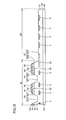
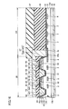
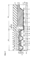
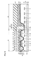
- FIG. 1 is a schematic plan view showing a configuration of a silicon carbide semiconductor device according to a first embodiment of the present invention.
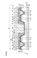
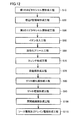
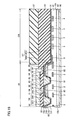
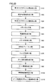
- FIG. 3 is a schematic cross-sectional view in a region III-III in FIG. It is a flowchart which shows schematically the manufacturing method of the silicon carbide semiconductor device which concerns on Embodiment 1 of this invention.
- FIG. 3 is a schematic cross sectional view schematically showing a first step of the method for manufacturing the silicon carbide semiconductor device according to the first embodiment of the present invention.
- FIG. 6 is a schematic plan view showing the configuration of a silicon carbide semiconductor device according to a second embodiment of the present invention. It is a cross-sectional schematic diagram which shows the structure of the silicon carbide semiconductor device which concerns on Embodiment 3 of this invention.
- Silicon carbide semiconductor device 1 includes a silicon carbide layer 10.
- Silicon carbide layer 10 has a first main surface 10b and a second main surface 10a opposite to first main surface 10b.
- Silicon carbide layer 10 includes a drift region 81, a body region 82, and a source region 83.
- Drift region 81 forms first main surface 10b and has the first conductivity type.
- Body region 82 is provided on drift region 81 and has a second conductivity type different from the first conductivity type.
- Source region 83 is provided on body region 82 so as to be separated from drift region 81, forms second main surface 10a, and has the first conductivity type.
- Silicon carbide layer 10 includes first side wall portion SW1 extending from second main surface 10a through source region 83 and body region 82 to drift region 81, and first bottom portion BT1 located in drift region 81.
- a trench TR made of is provided.
- Silicon carbide layer 10 includes a second conductivity type region 2 which is buried in and disposed in drift region 81 so as to face first bottom portion BT1 and has the second conductivity type. Second conductivity type region 2 is electrically connected to source region 83.
- silicon carbide layer 10 is arranged embedded in drift region 81 so as to face first bottom portion BT1 of trench TR, and has the second conductivity type.
- the second conductivity type region 2 is included.
- the second conductivity type region 2 is electrically connected to the source region 83.
- second conductivity type region 2 has a network structure in plan view. Thereby, the electric field concentration in the corner portion 81a of the trench TR can be relaxed while ensuring a wide current path.
- metal region 96 is further provided.
- Metal region 96 is in contact with source region 83.
- the source region 83 and the second conductivity type region 2 are electrically connected via the metal region 96.
- the switching characteristic of a silicon carbide semiconductor device can be improved effectively.
- that the source region 83 and the second conductivity type region 2 are electrically connected via the metal region 96 means that a part of the electric circuit connecting the source region 83 and the second conductivity type region 2 is used.
- the metal region 96 is included, and includes the case where the electric circuit connecting the source region 83 and the second conductivity type region 2 has a conductive region other than the metal region 96.
- silicon carbide layer 10 includes second bottom portion BT2 positioned between first main surface 10b and second main surface 10a, and A stepped portion ST including a second side wall portion SW2 connecting the second bottom portion BT2 and the second main surface 10a is provided.
- Metal region 96 is in contact with source region 83 on second main surface 10a and in contact with second bottom portion BT2. Thereby, the second conductivity type region 2 can be effectively electrically connected to the source region 83.
- silicon carbide layer 10 includes termination region OR and element region IR surrounded by termination region OR.
- the stepped portion ST is provided in the termination region OR.
- the second conductivity type region 2 can be electrically connected to the source region 83 while ensuring a large element region IR.
- termination region OR has guard ring region 3 having the second conductivity type.
- Metal region 96 is in contact with guard ring region 3 at second bottom portion BT 2, and guard ring region 3 is in contact with second conductivity type region 2.
- the breakdown voltage of the silicon carbide semiconductor device can be improved.
- termination region OR includes field stop region 4 surrounding guard ring region 3 in plan view and having the first conductivity type. Field stop region 4 is separated from second main surface 10a. Thereby, the breakdown voltage of the silicon carbide semiconductor device can be further improved.
- metal region 96 is in direct contact with second conductivity type region 2 at second bottom portion BT2. Thereby, the switching characteristics of the silicon carbide semiconductor device can be further improved.
- silicon carbide layer 10 includes termination region OR and element region IR surrounded by termination region OR.
- the stepped portion ST is provided in the element region IR.
- metal region 96 is in direct contact with second conductivity type region 2 at second bottom portion BT2. Thereby, the switching characteristics of the silicon carbide semiconductor device can be further improved.
- source region 83 is connected to second conductivity type region 2 through body region 82 and JTE region 5 having the second conductivity type. Touching. Thereby, since it is not necessary to form metal region 96 for connecting source region 83 and the second conductivity type region, the manufacturing process of silicon carbide semiconductor device 1 is simplified.
- first bottom portion BT1 of trench TR extends so as to surround polygonal cell CL in plan view.
- the second conductivity type region 2 is arranged at a position where the apex 81a of the cell CL overlaps the second conductivity type region 2.
- the apex 81a of the cell CL is a portion where the electric field is particularly concentrated in the corner portion of the trench TR.
- the method for manufacturing silicon carbide semiconductor device 1 includes the following steps.
- a silicon carbide layer 10 having a first main surface 10b and a second main surface 10a opposite to the first main surface 10b is prepared.
- Trench TR is formed in second main surface 10a of silicon carbide layer 10.
- Silicon carbide layer 10 includes a drift region 81, a body region 82, and a source region 83.
- Drift region 81 forms first main surface 10b and has the first conductivity type.
- Body region 82 is provided on drift region 81 and has a second conductivity type different from the first conductivity type.
- Source region 83 is provided on body region 82 so as to be separated from drift region 81, forms second main surface 10a, and has the first conductivity type.
- Trench TR is composed of first side wall portion SW1 extending from second main surface 10a through source region 83 and body region 82 to drift region 81, and first bottom portion BT1 located in drift region 81.
- Silicon carbide layer 10 includes a second conductivity type region 2 which is buried in and disposed in drift region 81 so as to face first bottom portion BT1 and has the second conductivity type. Second conductivity type region 2 is electrically connected to source region 83.
- silicon carbide layer 10 is buried and arranged in drift region 81 so as to face first bottom portion BT1 of trench TR, and the second A second conductivity type region 2 having a conductivity type is included.
- the electric field concentration in the corner portion 81a where the first bottom portion BT1 of the trench TR and the first sidewall portion SW1 are in contact can be effectively reduced.
- the breakdown voltage of the silicon carbide semiconductor device can be effectively improved.
- the second conductivity type region 2 is electrically connected to the source region 83. As a result, depletion at the time of applying the drain voltage is promoted, thereby facilitating a decrease in capacitance. Therefore, the high speed response of the silicon carbide semiconductor device is improved and the switching characteristics are improved.
- a stepped portion ST is formed which includes the second bottom portion BT2 located at the second bottom portion BT2 and the second side wall portion SW2 connecting the second bottom portion BT2 and the second main surface 10a.
- a metal region 96 in contact with the source region 83 and the second bottom portion BT2 is formed. Thereby, the 2nd conductivity type area
- region 2 can be effectively electrically connected with the source region 83 by this.
- MOSFET 1 As the silicon carbide semiconductor device of the first embodiment will be described.
- MOSFET 1 according to the first embodiment includes silicon carbide layer 10, silicon carbide single crystal substrate 80, gate insulating film 91, gate electrode 92, interlayer insulating film 93, metal region 96, and drain electrode 98. Have.
- the silicon carbide layer 10 is an epitaxial layer made of silicon carbide having a first main surface 10b and a second main surface 10a opposite to the first main surface.
- Silicon carbide single crystal substrate 80 is made of, for example, a hexagonal silicon carbide single crystal having polytype 4H.
- First main surface 10 b of silicon carbide layer 10 is in contact with silicon carbide single crystal substrate 80.
- Silicon carbide layer 10 mainly has a drift region 81, a body region 82, a source region 83, a contact region 84, a p-type region 2, and a connection region 2a.
- Silicon carbide layer 10 includes element region IR and termination region OR (see FIG. 10) surrounding element region IR.
- the termination region OR may have a guard ring region 3 (see FIG. 10) and a field stop region 4 (see FIG. 10).
- Drift region 81 is an n-type (first conductivity type) region containing an impurity such as nitrogen, for example.
- Drift region 81 forms first main surface 10 b of silicon carbide layer 10.
- the drift region 81 has a lower drift region 81c and an upper drift region 81d.
- the upper drift region 81d is provided on the lower drift region 81c.
- the p-type region 2 is partially provided in contact with the boundary surface between the lower drift region 81c and the upper drift region 81d.
- the impurity concentration of drift region 81 is preferably lower than the impurity concentration of silicon carbide single crystal substrate 80.
- the donor concentration in the drift region 81 is preferably 1 ⁇ 10 15 cm ⁇ 3 or more and 5 ⁇ 10 16 cm ⁇ 3 or less, for example, 8 ⁇ 10 15 cm ⁇ 3 .
- the thicknesses of the lower drift region 81c and the upper drift region 81d are, for example, 9 ⁇ m and 3 ⁇ m, respectively.
- Body region 82 is a p-type (second conductivity type) region containing an impurity such as aluminum or boron. Body region 82 is provided on upper drift region 81d.
- the acceptor concentration of body region 82 is preferably 1 ⁇ 10 17 cm ⁇ 3 or more and 5 ⁇ 10 18 cm ⁇ 3 or less. The acceptor concentration in body region 82 is higher than the donor concentration in drift region 81.
- Source region 83 is an n-type region containing an impurity such as phosphorus. Source region 83 is provided on body region 82 so as to be separated from drift region 81 by body region 82.
- the donor concentration of the source region 83 is, for example, about 2 ⁇ 10 19 cm ⁇ 3 .
- the donor concentration in the source region 83 is higher than the acceptor concentration in the body region 82.
- Source region 83 forms second main surface 10 a of silicon carbide layer 10 together with contact region 84.
- Contact region 84 is a p-type region containing an impurity such as aluminum.
- the contact region 84 is provided surrounded by the source region 83 and is connected to the body region 82.
- the acceptor concentration in contact region 84 is higher than the acceptor concentration in body region 82.
- the acceptor concentration of contact region 84 is, for example, about 1 ⁇ 10 20 cm ⁇ 3 .
- the contact region 84, the source region 84, the body region 82, and the drift region 81 form a cell CL.
- a (gate) trench TR is provided on the second main surface 10a of the silicon carbide layer 10.
- Trench TR includes first side wall portion SW1 and first bottom portion BT1.
- First sidewall portion SW1 extends from second main surface 10a of silicon carbide layer 10 through source region 83 and body region 82 to upper drift region 81d.
- the first bottom part BT1 is connected to the first side wall part SW1 and is located in the upper drift region 81d.
- First side wall portion SW ⁇ b> 1 includes a channel surface of MOSFET 1 on body region 82.
- First side wall portion SW1 is inclined with respect to second main surface 10a of silicon carbide layer 10.
- the trench TR extends in a tapered shape toward the opening.
- first bottom portion BT1 is substantially parallel to second main surface 10a and has a flat shape.
- a portion where the first bottom portion BT1 and the first sidewall portion SW1 are connected is a corner portion 81b of the trench TR.
- Silicon carbide layer 10 includes a second bottom portion BT2 positioned between first main surface 10b and second main surface 10a of silicon carbide layer 10, second bottom portion BT2, and second main surface 10a. Is provided with a stepped portion ST including a second side wall portion SW2 connecting the two.
- the stepped portion ST is provided in the element region IR.
- the second bottom portion BT2 of the stepped portion ST is provided at a position closer to the first main surface 10b than the first bottom portion BT1 of the trench TR.
- the width of the second bottom portion BT2 of the stepped portion ST is wider than the width of the first bottom portion BT1 of the trench TR.
- the stepped portion ST is provided so as not to form a part of the plurality of cells CL provided in the element region IR.
- the number of stepped portions ST is smaller than the number of cells CL.
- Each of p type region 2 (second conductivity type region) and connection region 2a is a p type region containing an impurity such as aluminum.
- the p-type region 2 is provided so as to be embedded in the drift region 81.
- the p-type region 2 is provided apart from the first bottom portion BT1 of the trench TR.
- p type region 2 is located closer to first main surface 10b than first bottom portion BT1 of trench TR.
- p-type region 2 is separated from body region 82 by 1 ⁇ m or more and 5 ⁇ m or less.
- each of p-type region 2 and connection region 2a is, for example, 1 ⁇ 10 12 cm ⁇ 2 or more and 1 ⁇ 10 15 cm ⁇ 2 or less, preferably 1 ⁇ 10 13 cm ⁇ 2 or more and 5 ⁇ 10 13 cm. -2 or less.
- Connection region 2a is provided in contact with second bottom portion BT2 of stepped portion ST.
- the connection region 2a and the p-type region 2 may be the p-type region 2 that is substantially integrated by being formed at the same time, for example. In this case, the metal region 96 is directly connected to the p-type region 2.
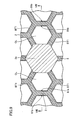
- FIG. 2 is a cross-sectional view of MOSFET 1 in the region II-II in FIG.
- p-type region 2 has a network structure in a plan view (a visual field in the normal direction of first main surface 10 b).
- a hexagonal (polygonal) portion surrounded by a broken line is a planar shape of the upper drift region 81 d viewed at the position of the first bottom portion BT ⁇ b> 1 of the trench TR.
- a region sandwiched between adjacent hexagonal cells CL is the first bottom portion BT1 of the trench TR.
- the first bottom portion BT1 of the trench TR extends so as to surround the hexagonal (polygonal) cell CL in plan view.
- the p-type region 2 is arranged at a position where each of the vertices 81 a of the hexagonal (polygonal) cell CL overlaps the p-type region 2.
- the first sidewall portion SW1 and the first bottom portion BT1 of the trench TR intersect with each other, and the vertex 81a of the hexagonal cell CL is the first corner portion 81a of the trench TR and is adjacent to the hexagon.
- a portion located in the middle of the two apexes is the second corner portion 81b of the trench TR.
- the first corner portion 81a is more likely to concentrate on the electric field than the second corner portion 81b, and the electric field strength is increased.
- p-type region 2 is provided at a position that overlaps with first corner portion 81a of trench TR and at a position that does not overlap with second corner portion 81b of trench TR. Thereby, the electric field concentration in the first corner portion 81a of the trench TR can be effectively reduced while securing the current path.
- the first bottom portion BT1 of the trench TR has a honeycomb structure.
- the p-type region 2 is disposed at a position overlapping the intersection IS of the honeycomb structure, and has a shape that does not overlap with a part of a line segment connecting two adjacent intersections IS of the honeycomb structure. It has a network structure.
- the connection region 2a has, for example, a hexagonal (polygonal) shape. As shown in FIG. 2, the connection region 2a is in contact with the p-type region 2 at each of the hexagonal vertices.
- FIG. 3 is a cross-sectional view of the MOSFET 1 in the region III-III in FIG.
- p-type region 2 is provided at a position facing a part of first bottom portion BT ⁇ b> 1 of trench TR in a cross-sectional view.
- the p-type region 2 and the first bottom portion BT1 of the trench TR partially overlap in plan view.
- the p-type region 2 is provided at a position facing the source region 83 and the body region 82.
- the p-type region 2 is disposed on the tangent line between the first side wall portion SW1 and the first bottom portion BT1 of the trench TR and facing the apex 81a of the hexagonal cell CL.
- gate insulating film 91 covers each of first side wall portion SW1 and first bottom portion BT1 of trench TR. Gate insulating film 91 is provided on body region 82 so as to connect source region 83 and upper drift region 81d. The gate insulating film 91 may be in contact with the second sidewall portion SW2 and the second bottom portion BT2 that form the stepped portion ST. Gate electrode 92 is in contact with gate insulating film 91 and is provided inside trench TR. The interlayer insulating film 93 is provided in contact with the gate electrode 92 and the gate insulating film 91 and electrically insulates the gate electrode 92 and the source electrode 94 from each other.
- the interlayer insulating film 93 may be disposed on the gate insulating film 91 provided in contact with the second side wall portion SW2 and the second bottom portion BT2 that form the stepped portion ST.
- Interlayer insulating film 93 is made of, for example, silicon dioxide.
- the metal region 96 includes a source electrode 94, a source wiring layer 95, and a contact electrode 94a.
- Source electrode 94 is in contact with each of source region 83 and contact region 84.
- the source wiring layer 95 is disposed on and in contact with the source electrode 94.
- Source wiring layer 95 is, for example, an aluminum layer.
- the interlayer insulating film 93 insulates between the gate electrode 92 and the source wiring layer 95.
- the contact electrode 94a is in contact with the connection region 2a at the second bottom portion BT2 of the stepped portion ST.
- the contact electrode 94a may be in contact with the gate insulating film 91.
- the source wiring layer 95 enters the stepped portion ST across the interlayer insulating film 93 from the source electrode 94 and is in contact with the contact electrode 94a.
- Metal region 96 is in contact with source region 83 and contact region 84 on second main surface 10a of silicon carbide layer 10 and is in contact with second bottom portion BT2 of stepped portion ST.
- the source region 83 is electrically connected to the p-type region 2 through the metal region 96.
- the source region 83 is in ohmic contact with the source electrode 94.
- Source region 83 is electrically connected to p-type region 2 via source electrode 94, source wiring layer 95, contact electrode 94a, and connection region 2a.
- each of first sidewall portion SW1 of trench TR and second sidewall portion SW2 of stepped portion ST includes a special surface.
- the special plane is a plane including the first plane having the plane orientation ⁇ 0-33-8 ⁇ . More preferably, the special surface includes the first surface microscopically and further includes the second surface having the surface orientation ⁇ 0-11-1 ⁇ microscopically. More preferably, the first surface and the second surface include a composite surface having a surface orientation ⁇ 0-11-2 ⁇ .
- the special surface is a surface having an off angle of 62 ° ⁇ 10 ° macroscopically with respect to the ⁇ 000-1 ⁇ surface.
- MOSFET 1 that is the silicon carbide semiconductor device according to the present embodiment
- the first epitaxial layer forming step (FIG. 4: S10) is performed.
- lower drift region 81 c that is a part of drift region 81 (FIG. 1) is formed on silicon carbide single crystal substrate 80.
- lower drift region 81 c is formed on silicon carbide single crystal substrate 80 by epitaxial growth.
- This epitaxial growth is performed by a CVD (Chemical Vapor Deposition) method using, for example, a mixed gas of silane (SiH 4 ) and propane (C 3 H 8 ) as a source gas and using, for example, hydrogen gas (H 2 ) as a carrier gas. be able to.
- CVD Chemical Vapor Deposition
- impurities such as nitrogen (N) and phosphorus (P) as impurities.
- concentration of impurities such as nitrogen contained in lower drift region 81c is, for example, about 7.0 ⁇ 10 15 cm 3 .
- the thickness of lower drift region 81c is, for example, about 9 ⁇ m.
- a buried p-type region forming step (FIG. 4: S20) is performed.
- a p-type region 2 having a p-type conductivity is formed on a part of lower drift region 81c.
- the lower drift region 81c is implanted with acceptor ions such as aluminum (impurity ions for imparting the second conductivity type) using an implantation mask (not shown).
- P-type region 2 is formed.
- the dose of aluminum ions is, for example, about 3 ⁇ 10 13 cm ⁇ 2 .
- a second epitaxial layer forming step (FIG. 4: S30) is performed.
- an upper drift region 81d having an n-type is formed on the lower drift region 81c having an n-type.
- p type region 2 is buried in drift region 81 constituted by lower drift region 81c and upper drift region 81d.
- the upper drift region 81d can be formed by a method similar to the method for forming the lower drift region 81c.
- the concentration of impurities such as nitrogen contained in upper drift region 81d is, for example, about 1.0 ⁇ 10 16 cm 3 .
- the thickness of the upper drift region 81d is, for example, about 3 ⁇ m.
- the body region 82 and the source region 83 are formed on the drift region 81. These formations can be performed by ion implantation into the drift region 81, for example.
- an impurity for imparting p-type such as aluminum (Al)
- Al aluminum
- an impurity for imparting n-type such as phosphorus (P)
- epitaxial growth may be used with the addition of impurities.
- Drift region 81, body region 82, source region 83, contact region 84, and p-type region 2 constitute silicon carbide layer 10 having first main surface 10b and second main surface 10a.
- Drift region 81 forms first main surface 10b
- source region 83 forms second main surface 10a.
- a step portion forming step (FIG. 5: S40) is performed. Specifically, a mask layer (not shown) having an opening is formed on second main surface 10 a made of source region 83. For example, a silicon oxide film or the like can be used as the mask layer. The opening is formed corresponding to the position of the step ST (FIG. 1).
- the source region 83, the body region 82, and a part of the drift region 81 are removed by etching.
- etching method for example, reactive ion etching (RIE), in particular, inductively coupled plasma (ICP) RIE can be used.
- ICP-RIE using SF 6 or a mixed gas of SF 6 and O 2 as a reaction gas can be used.
- thermal etching is performed in the recess.
- the thermal etching can be performed, for example, by heating in an atmosphere containing a reactive gas having at least one or more types of halogen atoms.
- the at least one or more types of halogen atom includes at least one of a chlorine (Cl) atom and a fluorine (F) atom.
- This atmosphere is, for example, Cl 2 , BCL 3 , SF 6 , or CF 4 .
- thermal etching is performed using a mixed gas of chlorine gas and oxygen gas as a reaction gas and a heat treatment temperature of, for example, 700 ° C. or more and 1000 ° C. or less.
- the reaction gas may contain a carrier gas in addition to the above-described chlorine gas and oxygen gas.
- a carrier gas for example, nitrogen (N 2 ) gas, argon gas, helium gas or the like can be used.
- the SiC etching rate is, for example, about 70 ⁇ m / hour.
- the mask layer made of silicon oxide has a very high selectivity with respect to SiC, so that it is not substantially etched during the etching of SiC.
- a stepped portion ST is formed on second main surface 10a of silicon carbide layer 10 by the above-described thermal etching.
- the stepped portion ST has a second side wall portion SW2 that passes through the source region 83 and the body region 82 and reaches the drift region 81, and a second bottom portion BT2 located on the drift region 81.
- the above-described special surface is self-formed on the second side wall portion SW2, particularly on the body region 82.
- the mask layer is removed by an arbitrary method such as etching.
- an ion implantation step (FIG. 4: S50) is performed.
- An ion implantation mask layer having an opening in a region where contact region 84 (FIG. 1) and connection region 2 a (FIG. 1) are formed is formed on second main surface 10 a of silicon carbide layer 10.
- Aluminum ions or the like are ion-implanted into silicon carbide layer 10 using the mask layer, thereby forming contact region 84 and connection region 2a having p-type conductivity. Note that the formation of the contact region 84 and the connection region 2a may be performed simultaneously or separately.
- an activation annealing step (FIG. 4: S60) is performed.
- heat treatment is performed on silicon carbide layer 10.
- the temperature of this heat treatment is preferably 1500 ° C. or higher and 1900 ° C. or lower, for example, about 1700 ° C.
- the heat treatment time is, for example, about 30 minutes.
- the atmosphere of the heat treatment is preferably an inert gas atmosphere, for example, an Ar atmosphere.
- a trench formation step (FIG. 5: S70) is performed.
- the trench forming step can be performed by the same method as the step portion forming step (FIG. 5: S40) described above.
- a mask layer having an opening is formed on the surface composed of source region 83 and contact region 84.
- a silicon oxide film or the like can be used as the mask layer.
- the opening is formed corresponding to the position of trench TR (FIG. 1).
- the source region 83, the body region 82, and a part of the drift region 81 are removed by etching.
- Etching is performed using, for example, ICP-RIE using SF 6 or a mixed gas of SF 6 and O 2 as a reaction gas.
- a recess having a side wall substantially perpendicular to the second main surface 10a is formed in a region where the trench TR (FIG. 1) is to be formed.
- thermal etching is performed in the recess.
- the thermal etching can be performed, for example, by heating in an atmosphere containing a reactive gas having at least one or more types of halogen atoms.
- the at least one or more types of halogen atom includes at least one of a chlorine (Cl) atom and a fluorine (F) atom.
- This atmosphere is, for example, Cl 2 , BCL 3 , SF 6 , or CF 4 .
- thermal etching is performed using a mixed gas of chlorine gas and oxygen gas as a reaction gas and a heat treatment temperature of, for example, 700 ° C. or more and 1000 ° C. or less.
- the reaction gas may contain a carrier gas in addition to the above-described chlorine gas and oxygen gas.
- the carrier gas for example, nitrogen (N 2 ) gas, argon gas, helium gas or the like can be used.
- the trench TR is formed on second main surface 10a of silicon carbide layer 10 by the above-described thermal etching.
- Trench TR has a first sidewall portion SW1 that penetrates source region 83 and body region 82 to reach drift region 81, and a first bottom portion BT 1 that is located on drift region 81.
- Each of first side wall portion SW1 and first bottom portion BT1 is separated from p-type region 2.
- a special surface is self-formed on the first side wall portion SW1, particularly on the body region 82.
- the mask layer is removed by an arbitrary method such as etching.
- the trench formation step (FIG. 4: S70) and the step portion formation step (FIG. 4: S40) are both performed by thermal etching, but the thermal etching time in the step portion formation step is the heat in the trench formation step. It may be longer than the etching time. Accordingly, the second bottom portion BT2 forming the stepped portion ST is formed at a position closer to the first main surface 10b than the first bottom portion BT1 of the trench TR. Depth of trench TR, in other words, between second main surface 10a of silicon carbide layer 10 and first bottom portion BT1 of trench TR along the normal direction of first main surface 10b of silicon carbide layer 10. The distance is, for example, about 1.0 ⁇ m to 1.8 ⁇ m.
- Depth of stepped portion ST in other words, second main surface 10a of silicon carbide layer 10 and second bottom portion BT2 of stepped portion ST along the normal direction of first main surface 10b of silicon carbide layer 10. Is about 1.1 ⁇ m to 3.0 ⁇ m, for example.
- Gate insulating film 91 is formed to cover first sidewall portion SW1 and first bottom portion BT1 of trench TR, and to cover second sidewall portion SW2 and second bottom portion BT2 of stepped portion ST.
- the gate insulating film 91 can be formed by thermal oxidation, for example.
- NO annealing using nitrogen monoxide (NO) gas as the atmospheric gas may be performed.
- the temperature profile has, for example, conditions of a temperature of 1100 ° C. to 1300 ° C. and a holding time of about 1 hour.
- nitrogen atoms are introduced into the interface region between the gate insulating film 91 and the body region 82.
- a gas other than NO gas may be used as the atmospheric gas.
- Ar annealing using argon (Ar) as an atmospheric gas may be further performed after the NO annealing.
- the heating temperature for Ar annealing is preferably the same as or higher than the heating temperature for NO annealing, and is lower than the melting point of the gate insulating film 91.
- the time during which this heating temperature is maintained is, for example, about 1 hour. Thereby, the formation of the interface state in the interface region between the gate insulating film 91 and the body region 82 is further suppressed.
- other inert gas such as nitrogen gas may be used as the atmospheric gas instead of Ar gas.
- a gate electrode formation step (FIG. 4: S90) is performed.
- a gate electrode 92 in contact with the gate insulating film 91 is formed.
- gate electrode 92 is formed on gate insulating film 91 so as to fill the region inside trench TR with gate electrode 92.
- the formation method of the gate electrode 92 can be performed by, for example, forming a conductor or doped polysilicon and performing CMP (Chemical Mechanical Polishing).
- Interlayer insulating film 93 is formed on gate electrode 92 and gate insulating film 91 so as to cover the exposed surface of gate electrode 92.
- Interlayer insulating film 93 is formed on and in contact with gate insulating film 93 formed on second side wall portion SW2 and second bottom portion BT2 that form stepped portion ST.
- a source electrode and drain electrode formation step (FIG. 4: S110) is performed.
- the interlayer insulating film 93 and the gate insulating film 91 are etched so that openings are formed in the interlayer insulating film 93 and the gate insulating film 91. Through this opening, each of source region 83 and contact region 84 is exposed on second main surface 10a.
- source electrode 94 in contact with each of source region 83 and contact region 84 is formed on second main surface 10a.
- the gate insulating film 91 and the interlayer insulating film 93 are etched so that the connection region 2a is exposed at the second bottom portion BT2 of the stepped portion ST.
- a contact electrode 94a in contact with the connection region 2a is formed at the second bottom portion BT2 of the stepped portion ST.
- the formation of the contact electrode 94a may be performed simultaneously with the formation of the source electrode 94, or may be performed separately.
- the source wiring layer 95 is formed in contact with the source electrode 94, the contact electrode 94a, and the interlayer insulating film 93.
- the metal region 96 that is in contact with the source region 83 and the second bottom portion BT2 of the stepped portion ST is formed.
- drain electrode 98 is formed on first main surface 10 b formed of drift region 81 through silicon carbide single crystal substrate 80.
- MOSFET 1 as the silicon carbide semiconductor device according to the first embodiment
- MOSFET 1 silicon carbide layer 10 is embedded in drift region 81 so as to oppose first bottom portion BT1 of trench TR, and p-type region 2 having p-type is provided. Including. Thereby, the electric field concentration in the corner portion 81a where the first bottom portion BT1 of the trench TR and the first sidewall portion SW1 are in contact can be effectively reduced. As a result, the breakdown voltage of MOSFET 1 can be effectively improved.
- the p-type region 2 is electrically connected to the source region 83. As a result, depletion at the time of applying the drain voltage is promoted, thereby facilitating a decrease in capacitance. Therefore, the high speed response of the MOSFET 1 is improved and the switching characteristics are improved.
- p-type region 2 has a network structure in plan view. Thereby, the electric field concentration in the corner portion 81a of the trench TR can be relaxed while ensuring a wide current path. Further, the p-type region 2 is integrally spread in the drift region 81 so as to have a network structure. When a plurality of p-type regions 2 exist and are isolated from each other, it is necessary to electrically connect each p-type region 2 to the source electrode 94. In this case, it is necessary to form a large number of source trenches for electrically connecting to the source electrode 94 for each of the plurality of p-type regions 2.
- MOSFET 1 according to the first embodiment, p-type region 2 is integrated so as to have a network structure. Therefore, it is not necessary to provide a large number of source trenches in order to electrically connect p-type region 2 and source electrode 94, so that the cell pitch of MOSFET 1 can be reduced. As a result, the on-resistance of MOSFET 1 can be reduced.
- the MOSFET 1 according to the first embodiment further includes the metal region 96.
- Metal region 96 is in contact with source region 83.
- Source region 83 and p-type region 2 are electrically connected via metal region 96. Thereby, the switching characteristic of MOSFET1 can be improved effectively.
- silicon carbide layer 10 includes second bottom portion BT2 and second bottom portion BT2 located between first main surface 10b and second main surface 10a. And a second side wall portion SW2 that connects the second main surface 10a to each other is provided.
- Metal region 96 is in contact with source region 83 on second main surface 10a and in contact with second bottom portion BT2. Thereby, p type region 2 can be effectively electrically connected to source region 83.
- silicon carbide layer 10 includes termination region OR and element region IR surrounded by termination region OR.
- the stepped portion ST is provided in the element region IR.
- metal region 96 is in direct contact with p-type region 2 at second bottom portion BT2. Thereby, the switching characteristic of MOSFET1 can be improved more.
- first bottom portion of trench TR extends to surround polygonal cell CL in plan view, and apex 81a of cell CL is p in plan view.
- a p-type region 2 is arranged at a position overlapping the mold region 2.
- the apex 81a of the cell CL is a portion where the electric field is particularly concentrated in the corner portion of the trench TR.
- silicon carbide layer 10 is buried in drift region 81 so as to face first bottom portion BT1 of trench TR, and has a p-type. Region 2 is included. Thereby, the electric field concentration in the corner portion 81a where the first bottom portion BT1 of the trench TR and the first sidewall portion SW1 are in contact can be effectively reduced. As a result, the breakdown voltage of MOSFET 1 can be effectively improved.
- the p-type region 2 is electrically connected to the source region 83. As a result, depletion at the time of applying the drain voltage is promoted, thereby facilitating a decrease in capacitance. Therefore, the high speed response of the MOSFET 1 is improved and the switching characteristics are improved.
- second main surface 10a of silicon carbide layer 10 has a second main surface 10a and a second main surface 10a located between first main surface 10b and second main surface 10a.
- a stepped portion ST including the bottom portion BT2 and the second side wall portion SW2 connecting the second bottom portion BT2 and the second main surface 10a is formed.
- a metal region 96 in contact with the source region 83 and the second bottom portion BT2 is formed. Thereby, p type region 2 can be effectively electrically connected to source region 83.
- the stepped portion ST is formed by thermal etching. Thereby, the stepped portion ST can be effectively formed.
- Emodiment 2 Next, the configuration of MOSFET 1 according to the second embodiment will be described.
- the configuration of MOSFET 1 according to the second embodiment is different from the configuration of MOSFET 1 according to the first embodiment mainly in the shape of p-type region 2, and the other configuration is substantially the same as that of MOSFET 1 according to the first embodiment. Have.
- the following description will focus on the differences from the configuration of MOSFET 1 according to the first embodiment.
- p-type region 2 of MOSFET 1 is provided at a position facing first bottom portion BT1 of trench TR.
- the width of the p-type region 2 along the direction parallel to the first major surface 10b may be smaller than the width of the first bottom portion BT1 of the trench TR.
- the connection region 2a is provided in contact with the contact electrode 94a.
- Connection region 2a may be in contact with gate insulating film 91 at second bottom portion BT2 of stepped portion ST.
- the width of the connection region 2a along the direction parallel to the first main surface 10b may be larger than the width of the contact electrode 94a.
- FIG. 9 shows a surface of the MOSFET 1 cut along the region IX-IX in FIG.
- p-type region 2 has a mesh structure in plan view.
- a hexagonal (polygonal) portion surrounded by a broken line is the planar shape of the upper drift region 81d viewed at the position of the first bottom portion BT1 of the trench TR.
- a region sandwiched between adjacent hexagonal cells CL is the first bottom portion BT1 of the trench TR.
- the first bottom portion BT1 of the trench TR extends so as to surround the hexagonal cell CL in plan view.
- the p-type region 2 included in the MOSFET 1 according to the second embodiment is arranged so as to surround the hexagonal cell CL in plan view.
- the first bottom portion BT1 of the trench TR has a honeycomb structure.
- the p-type region 2 is provided so as to overlap with the first bottom portion BT1 of the trench TR in plan view. That is, the p-type region 2 also has a honeycomb structure.
- the connection region 2a has, for example, a hexagonal (polygonal) shape. As shown in FIG. 9, the connection region 2 a is in contact with the p-type region 2 at each of the hexagonal vertices. (Embodiment 3) Next, the configuration of MOSFET 1 according to the third embodiment will be described.
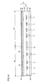
- the configuration of MOSFET 1 according to the third embodiment is different from the configuration of MOSFET 1 according to the first embodiment in that stepped portion ST of MOSFET 1 is provided in termination region OR, and the rest is substantially the same as MOSFET 1 according to the first embodiment. It has a configuration. The following description will focus on the differences from the configuration of MOSFET 1 according to the first embodiment.
- Silicon carbide layer 10 of MOSFET 1 includes termination region OR and element region IR surrounded by termination region OR.
- Termination region OR has a plurality of guard ring regions 3 provided so as to surround element region IR and a field stop region 4 provided so as to surround guard ring region 3 in plan view.
- Guard ring region 3 has the same conductivity type (second conductivity type) as p-type region 2. The dose amount of the guard ring region 3 may be smaller than the dose amount of the p-type region 2.
- the dose of acceptor ions such as aluminum ions in the guard ring region 3 is, for example, about 1.3 ⁇ 10 13 cm ⁇ 2
- the dose of acceptor ions such as aluminum ions in the p-type region 2 is, for example, 3.0. It is about ⁇ 10 13 cm -2 .
- Field stop region 4 is an n-type region into which, for example, phosphorus (P) or the like is ion-implanted.
- the dose amount of donor ions such as phosphorus ions in the field stop region 4 is, for example, about 1.0 ⁇ 10 13 cm ⁇ 2 .
- a stepped portion ST is provided on the second main surface 10a of the silicon carbide layer 10.
- Second bottom portion BT2 of stepped portion ST is provided in termination region OR of silicon carbide layer 10.
- An insulating film 91 is provided on the second bottom portion BT2 of the stepped portion ST, and an insulating film 93 is provided on the insulating film 91.
- Guard ring region 3 and field stop region 4 are in contact with insulating film 91 at second bottom portion BT2 of stepped portion ST.
- a protective film 97 is provided in contact with the insulating film 93 and the source wiring layer 95.
- the termination region OR is a region including the side end portion 10d of the silicon carbide layer 10, and is a region outside the cell arranged on the outermost side.
- the source wiring layer 95 includes a source electrode 94 in contact with the cell source region 83 and the contact region 84 provided in the element region IR, and a contact in contact with the second bottom portion BT2 of the stepped portion ST provided in the termination region OR.
- the electrode 94a is provided so as to be electrically connected.
- Connection region 2a is in contact with contact electrode 94a at second bottom portion BT2 of stepped portion ST.
- the connection region 2a may be provided so as to extend from the termination region OR to the element region IR.
- FIG. 11 shows a surface obtained by cutting the MOSFET in the region XI-XI in FIG.
- p-type region 2 has a mesh structure in plan view.
- a hexagonal (polygonal) portion surrounded by a broken line is the planar shape of the upper drift region 81d viewed at the position of the first bottom portion BT1 of the trench TR.
- a region sandwiched between adjacent hexagonal cells CL is the first bottom portion BT1 of the trench TR.
- the first bottom portion BT1 of the trench TR extends so as to surround the hexagonal cell CL in plan view.
- the p-type region 2 is arranged at a position where each of the vertices 81 a of the hexagonal cell CL overlaps the p-type region 2.
- the first bottom portion BT1 of the trench TR has a honeycomb structure.
- the p-type region is disposed at a position overlapping the intersection IS of the honeycomb structure, and has a mesh shape that does not overlap with a part of a line connecting the intersection IS of the honeycomb structure and the intersection IS. It has a structure.
- the connection region 2a has, for example, a hexagonal (polygonal) shape. As shown in FIG. 11, connection region 2a is in contact with p-type region 2 at the outer end of p-type region 2 in plan view.
- guard ring region 3 and a field stop region 4 are provided between the p-type region 2 and the side end portion 10d of the silicon carbide layer 10.
- Guard ring region 3 extends along a direction parallel to first main surface 10b so as to surround p type region 2 and connection region 2a.
- Field stop region 4 is provided on the side end portion 10 d side of silicon carbide layer 10 with respect to guard ring region 3.
- a part of the p-type region 2 may be provided in the termination region OR.
- MOSFET 1 that is the silicon carbide semiconductor device according to the third embodiment
- the first epitaxial layer forming step (FIG. 12: S10) is performed.
- the first epitaxial layer forming step is performed in the same manner as the method described in the first embodiment.
- lower drift region 81 c is formed on silicon carbide single crystal substrate 80.
- the concentration of impurities such as nitrogen contained in lower drift region 81c is, for example, about 7.0 ⁇ 10 15 cm 3 .
- the thickness of lower drift region 81c is, for example, about 9 ⁇ m.
- a buried p-type region forming step (FIG. 12: S20) is performed.
- a p-type region 2, a p-type connection region 2a, a p-type guard ring region 3, and an n-type field stop region are formed on a part of the lower drift region 81c. 4 are formed.
- acceptor ions such as aluminum
- p-type region 2, connection region 2a, guard ring Region 3 is formed.
- the dose of acceptor ions such as aluminum ions in the guard ring region 3 is, for example, about 1.3 to 1.5 ⁇ 10 13 cm ⁇ 2.
- the dose of acceptor ions such as aluminum ions in the p-type region 2 is For example, it is about 3.0 ⁇ 10 13 cm ⁇ 2 .
- a second epitaxial layer forming step (FIG. 12: S30) is performed.
- the n-type is formed on the lower drift region 81c having the n-type.
- An upper drift region 81d is formed.
- p-type region 2, connection region 2a, guard ring region 3, and field stop region 4 are buried in drift region 81 constituted by lower drift region 81c and upper drift region 81d.
- the upper drift region 81d can be formed by a method similar to the method for forming the lower drift region 81c.
- the concentration of impurities such as nitrogen contained in upper drift region 81d is, for example, about 1.0 ⁇ 10 16 cm 3 .
- the thickness of the upper drift region 81d is, for example, about 3 ⁇ m.
- an ion implantation step (FIG. 12: S50) is performed. Specifically, body region 82 and source region 83 are formed on drift region 81. These formations can be performed by ion implantation into the drift region 81, for example. In ion implantation for forming body region 82, an impurity for imparting p-type, such as aluminum (Al), is implanted. In the ion implantation for forming source region 83, an impurity for imparting n-type, such as phosphorus (P), is implanted. Instead of ion implantation, epitaxial growth may be used with the addition of impurities.
- ion implantation epitaxial growth may be used with the addition of impurities.
- an ion implantation mask layer having an opening in a region where contact region 84 (FIG. 10) is formed is formed on second main surface 10a of silicon carbide layer 10.
- aluminum ions or the like are ion-implanted into silicon carbide layer 10 to form contact region 84 having p-type conductivity.
- an activation annealing step (FIG. 12: S60) is performed.
- heat treatment is performed on silicon carbide layer 10.
- the temperature of this heat treatment is preferably 1500 ° C. or higher and 1900 ° C. or lower, for example, about 1700 ° C.
- the heat treatment time is, for example, about 30 minutes.
- the atmosphere of the heat treatment is preferably an inert gas atmosphere, for example, an Ar atmosphere.
- a trench formation step (FIG. 12: S70) is performed.
- the thermal etching described in the first embodiment is performed.
- trench TR is formed on second main surface 10a of silicon carbide layer 10.
- Trench TR has a first sidewall portion SW1 that penetrates source region 83 and body region 82 to reach drift region 81, and a first bottom portion BT 1 that is located on drift region 81.
- Each of first side wall portion SW1 and first bottom portion BT1 is separated from p-type region 2.
- a special surface is self-formed on the first side wall portion SW1, particularly on the body region 82.
- a step portion forming step (FIG. 12: S75) is performed.
- the thermal etching described in the first embodiment is performed.
- Step portion ST is formed on second main surface 10a of silicon carbide layer 10 by the thermal etching described above.
- the stepped portion ST has a second side wall portion SW2 that passes through the source region 83 and the body region 82 and reaches the drift region 81, and a second bottom portion BT2 located on the drift region 81.
- the above-described special surface is self-formed on the second side wall portion SW2, particularly on the body region 82.
- the stepped portion ST is formed such that a part of the connection region 2a, the guard ring region 3, and the field stop region 4 are exposed at the second bottom portion BT2 of the stepped portion ST.
- the stepped portion ST may be formed such that a part of the p-type region 2 is exposed at the second bottom portion BT2 of the stepped portion ST.
- silicon carbide layer 10 in which trench TR and stepped portion ST shown in FIG. 15 are formed is formed.
- Gate insulating film 91 is formed to cover first sidewall portion SW1 and first bottom portion BT1 of trench TR, and to cover second sidewall portion SW2 and second bottom portion BT2 of stepped portion ST.
- the gate insulating film 91 can be formed by thermal oxidation, for example.
- NO annealing using nitrogen monoxide (NO) gas as the atmospheric gas may be performed.
- a gate electrode formation step (FIG. 12: 90) is performed.
- a gate electrode 92 in contact with the gate insulating film 91 is formed.
- gate electrode 92 is formed on gate insulating film 91 so as to fill the region inside trench TR with gate electrode 92.
- the gate electrode 92 can be formed by, for example, conductor or doped polysilicon film formation and CMP.
- Interlayer insulating film 93 is formed on gate electrode 92 and gate insulating film 91 so as to cover the exposed surface of gate electrode 92.
- Interlayer insulating film 93 is formed on and in contact with gate insulating film 93 formed on second side wall portion SW2 and second bottom portion BT2 that form stepped portion ST.
- a source electrode and drain electrode formation step (FIG. 12: S110) is performed.
- the interlayer insulating film 93 and the gate insulating film 91 are etched so that openings are formed in the interlayer insulating film 93 and the gate insulating film 91. Through this opening, each of source region 83 and contact region 84 is exposed on second main surface 10a.
- source electrode 94 in contact with each of source region 83 and contact region 84 is formed on second main surface 10a.
- the gate insulating film 91 and the interlayer insulating film 93 are etched so that the connection region 2a is exposed at the second bottom portion BT2 of the stepped portion ST.
- a contact electrode 94a in contact with the connection region 2a is formed at the second bottom portion BT2 of the stepped portion ST.
- the formation of the contact electrode 94a may be performed simultaneously with the formation of the source electrode 94, or may be performed separately.
- the source wiring layer 95 is formed in contact with the source electrode 94, the contact electrode 94a, and the interlayer insulating film 93.
- drain electrode 98 is formed on first main surface 10 b formed of drift region 81 through silicon carbide single crystal substrate 80.
- silicon carbide layer 10 includes termination region OR and element region IR surrounded by termination region OR.
- the stepped portion ST is provided in the termination region OR.
- p-type region 2 can be electrically connected to source region 83 while ensuring a wide element region IR.
- connection region 2a is formed so as to surround p-type region 2 in plan view. 3 has substantially the same configuration as the MOSFET 1 of FIG. The following description will focus on the differences from the configuration of MOSFET 1 according to the third embodiment.
- silicon carbide layer 10 includes termination region OR and element region IR surrounded by termination region OR.
- Connection region 2a is provided in termination region OR, and may be connected to p-type region 2 at the boundary between termination region OR and element region IR.
- Connection region 2a is a guard ring region provided so as to surround p-type region 2 in plan view.
- the metal region 96 is in contact with the connection region 2a that is a guard ring region at the second bottom portion BT2 of the stepped portion ST.
- the connection region 2 a that is a guard ring region is in contact with the p-type region 2.
- the metal region 96 is connected to the p-type region 2 via the connection region 2a as a guard ring region.
- termination region OR has a guard ring region 3 having a p-type.
- Metal region 96 is in contact with guard ring region 3 at second bottom portion BT 2, and guard ring region 3 is in contact with p type region 2.
- the breakdown voltage of MOSFET 1 can be improved.
- FIG. 5 the configuration of MOSFET 1 according to the fifth embodiment will be described.
- MOSFET 1 according to the fifth embodiment is different from the configuration of MOSFET 1 according to the fourth embodiment in that a drift region 81 exists between the field stop region 4 and the gate insulating film 91, and the rest is implemented.
- the configuration is almost the same as that of the MOSFET 1 of the fourth embodiment.
- the following description will focus on the differences from the configuration of MOSFET 1 according to the fourth embodiment.
- Field stop region 4 of MOSFET 1 according to the fifth embodiment is provided apart from second main surface 10a of silicon carbide layer 10.
- the field stop region 4 may be separated from the second bottom portion BT2 of the stepped portion ST.
- the drift region 81 exists between the field stop region 4 and the gate insulating film 91.
- Second main surface 10a of silicon carbide layer 10 in contact with side end portion 10d of silicon carbide layer 10 is located farther from first main surface 10b of silicon carbide layer 10 than second bottom portion BT2 of stepped portion ST. Exists.
- termination region OR includes guard ring region 3 in plan view and includes field stop region 4 having an n-type. Field stop region 4 is separated from second main surface 10a. Thereby, the breakdown voltage of MOSFET 1 can be further improved.
- MOSFET 1 according to the sixth embodiment is implemented in that drift region 81 exists between guard ring region 3 and gate insulating film 91 and that metal region 96 is in direct contact with p-type region 2.
- the configuration is different from that of MOSFET 1 according to the fifth embodiment, and the other configuration is substantially the same as that of MOSFET 1 according to the fifth embodiment. The following description will focus on the differences from the configuration of MOSFET 1 according to the fifth embodiment.
- guard ring region 3 and field stop region 4 of MOSFET 1 according to the sixth embodiment are provided apart from second main surface 10a of silicon carbide layer 10.
- the guard ring region 3 may be separated from the second bottom portion BT2 of the stepped portion ST.
- Drift region 81 exists between guard ring region 3 and field stop region 4 and gate insulating film 91.
- Guard ring region 3 and field stop region 4 are embedded in drift region 81.
- the connection region is, for example, p-type region 2 that is substantially integrated with p-type region 2.
- Metal region 96 is in direct contact with p-type region 2 at second bottom portion BT2 of stepped portion ST.
- MOSFET 1 according to the sixth embodiment metal region 96 is in direct contact with p-type region 2 at second bottom portion BT2. Thereby, the switching characteristic of MOSFET1 can be improved more.
- FIG. 7 the configuration of MOSFET 1 according to the seventh embodiment will be described.
- MOSFET 1 according to the seventh embodiment has the configuration of MOSFET 1 according to the third embodiment in that it has a JTE (Junction Termination Extension) region and metal region 96 is not in contact with second bottom portion BT2 of stepped portion ST.
- the other configurations are substantially the same as those of the MOSFET 1 of the third embodiment. The following description will focus on the differences from the configuration of MOSFET 1 according to the third embodiment.
- MOSFET 1 as the silicon carbide semiconductor device of the seventh embodiment will be described.
- MOSFET 1 according to the seventh embodiment has JTE region 5.
- the JTE region 5 is a region having a p-type (second conductivity type).
- the dose amount of, for example, aluminum ions in the JTE region 5 is about 1.3 to 1.5 ⁇ 10 13 cm ⁇ 2 .
- JTE region 5 is in contact with gate insulating film 91 at second side wall portion SW2 and second bottom portion BT2 of stepped portion ST.
- JTE region 5 is in contact with p type region 2 and body region 82.
- Source electrode 94 is electrically connected to p type region 2 through contact region 84, body region 82, and JTE region 5.
- Contact region 84 is in contact with source region 83.
- the source region 83 is in ohmic contact with the source electrode 94.
- JTE region 5 may be provided so as to surround p-type region 2 in plan view.
- MOSFET 1 that is the silicon carbide semiconductor device according to the seventh embodiment
- the first epitaxial layer forming step (FIG. 20: S10) is performed.
- the first epitaxial layer forming step is performed in the same manner as the method described in the first embodiment.
- lower drift region 81 c is formed on silicon carbide single crystal substrate 80.
- the concentration of impurities such as nitrogen contained in lower drift region 81c is, for example, about 7.0 ⁇ 10 15 cm 3 .
- the thickness of lower drift region 81c is, for example, about 9 ⁇ m.
- a buried p-type region forming step (FIG. 20: S20) is performed.
- p-type region 2 is formed by implanting acceptor ions such as aluminum into lower drift region 81c using an implantation mask (not shown).
- the dose of aluminum ions is, for example, about 3 ⁇ 10 13 cm ⁇ 2 .
- a second epitaxial layer forming step (FIG. 20: S30) is performed.
- an upper drift region 81d having an n-type is formed on the lower drift region 81c having an n-type.
- p type region 2 is buried in drift region 81 constituted by lower drift region 81c and upper drift region 81d.
- the upper drift region 81d can be formed by a method similar to the method for forming the lower drift region 81c.
- the concentration of impurities such as nitrogen contained in upper drift region 81d is, for example, about 1.0 ⁇ 10 16 cm 3 .
- the thickness of the upper drift region 81d is, for example, about 3 ⁇ m.
- an ion implantation step (FIG. 20: S50) is performed. Specifically, body region 82 and source region 83 are formed on drift region 81. These formations can be performed by ion implantation into the drift region 81, for example. In ion implantation for forming body region 82, an impurity for imparting p-type, such as aluminum (Al), is implanted. In the ion implantation for forming source region 83, an impurity for imparting n-type, such as phosphorus (P), is implanted. Instead of ion implantation, epitaxial growth may be used with the addition of impurities.
- ion implantation epitaxial growth may be used with the addition of impurities.
- an ion implantation mask layer having an opening in a region where contact region 84 (FIG. 19) is formed is formed on second main surface 10a of silicon carbide layer 10.
- aluminum ions or the like are ion-implanted into silicon carbide layer 10 to form contact region 84 having p-type conductivity.
- a step portion forming step (FIG. 20: S55) is performed.
- the thermal etching described in the first embodiment is performed.
- Step portion ST is formed on second main surface 10a of silicon carbide layer 10 by the thermal etching described above.
- the stepped portion ST has a second side wall portion SW2 that passes through the source region 83 and the body region 82 and reaches the drift region 81, and a second bottom portion BT2 located on the drift region 81.
- the above-described special surface is self-formed on the second side wall portion SW2, particularly on the body region 82.
- a JTE and GR formation step (FIG. 20: S56) is performed. Specifically, the step is performed by implanting acceptor ions such as aluminum into the second bottom portion BT2 and the second sidewall portion SW2 of the step portion ST using an implantation mask (not shown). JTE region 5 in contact with second bottom portion BT2 and second side wall portion SW2 of portion ST and guard ring region 3 in contact with second bottom portion BT2 of stepped portion ST are formed.
- the dose of aluminum ions is, for example, about 1.3 ⁇ 10 13 cm ⁇ 2 .
- JTE region 5 is formed in contact with p type region 2 and body region 82.
- donor ions such as phosphorus ions are implanted into the second bottom portion BT2 of the stepped portion ST by using an implantation mask (not shown), thereby contacting the second bottom portion BT2 of the stepped portion ST.
- a field stop region 4 is formed.
- an activation annealing step (FIG. 20: S60) is performed.
- heat treatment is performed on silicon carbide layer 10.
- the temperature of this heat treatment is preferably 1500 ° C. or higher and 1900 ° C. or lower, for example, about 1700 ° C.
- the heat treatment time is, for example, about 30 minutes.
- the atmosphere of the heat treatment is preferably an inert gas atmosphere, for example, an Ar atmosphere.
- a trench formation step (FIG. 20: S70) is performed.
- the thermal etching described in the first embodiment is performed.
- trench TR is formed on second main surface 10a of silicon carbide layer 10.
- Trench TR has a first sidewall portion SW1 that penetrates source region 83 and body region 82 to reach drift region 81, and a first bottom portion BT 1 that is located on drift region 81.
- Each of first side wall portion SW1 and first bottom portion BT1 is separated from p-type region 2.
- a special surface is self-formed on the first side wall portion SW1, particularly on the body region 82.
- Gate insulating film 91 is formed to cover first sidewall portion SW1 and first bottom portion BT1 of trench TR, and to cover second sidewall portion SW2 and second bottom portion BT2 of stepped portion ST.
- the gate insulating film 91 can be formed by thermal oxidation, for example.
- NO annealing using nitrogen monoxide (NO) gas as the atmospheric gas may be performed.
- Gate insulating film 91 is formed in contact with JTE region 5, guard ring region 3, field stop region 4, body region 82, and source region 83.
- a gate electrode forming step (FIG. 20: 90) is performed.
- a gate electrode 92 in contact with the gate insulating film 91 is formed.
- gate electrode 92 is formed on gate insulating film 91 so as to fill the region inside trench TR with gate electrode 92.
- the gate electrode 92 can be formed by, for example, conductor or doped polysilicon film formation and CMP.
- Interlayer insulating film 93 is formed on gate electrode 92 and gate insulating film 91 so as to cover the exposed surface of gate electrode 92.
- Interlayer insulating film 93 is formed on and in contact with gate insulating film 93 formed on second side wall portion SW2 and second bottom portion BT2 that form stepped portion ST.
- a source electrode and drain electrode formation step (FIG. 20: S110) is performed.
- the interlayer insulating film 93 and the gate insulating film 91 are etched so that openings are formed in the interlayer insulating film 93 and the gate insulating film 91. Through this opening, each of source region 83 and contact region 84 is exposed on second main surface 10a.
- source electrode 94 in contact with each of source region 83 and n contact region 84 is formed on second main surface 10a.
- the source wiring layer 95 is formed in contact with the source electrode 94, the contact electrode 94a, and the interlayer insulating film 93.
- drain electrode 98 is formed on first main surface 10 b formed of drift region 81 through silicon carbide single crystal substrate 80.
- source region 83 is in contact with p type region 2 through body region 82 and JTE region 5 having p type. This eliminates the need to form the metal region 96 for connecting the source region 83 and the p-type region 2, thereby simplifying the manufacturing process of the MOSFET 1.
- the MOSFET is described as an example of the silicon carbide semiconductor device.
- the silicon carbide semiconductor device may be, for example, an IGBT (Insulated Gate Bipolar Transistor).
- the n-type is the first conductivity type and the p-type is the second conductivity type.
- the p-type may be the first conductivity type and the n-type may be the second conductivity type.
- 1 silicon carbide semiconductor device MOSFET
- 2nd conductivity type region p-type region
- 2a connection region 3 guard ring region, 4 field stop region
- 10 silicon carbide layer 10a second main surface, 10b first Main surface, 10d side edge, 80 silicon carbide single crystal substrate, 81 drift region, 81a first corner (vertex), 81b second corner, 81c lower drift region, 81d upper drift region, 82 body region 83 source region, 84 contact region, 91 gate insulating film (insulating film), 92 gate electrode, 93 interlayer insulating film, 94 source electrode, 94a contact electrode, 95 source wiring layer, 96 metal region, 97 protective film, 98 drain Electrode, BT1 first bottom, BT2 second bottom, CL cell, IR element region, IS Intersection, OR termination region, ST stepped portion, SW1 first side wall portion, SW2 a second side wall portion, TR trench.
Landscapes
- Electrodes Of Semiconductors (AREA)
Abstract
Selon la présente invention, une couche de carbure de silicium (10) comprend une région de dérive (81), une région de corps (82) et une région de source (83). La région de dérive (81) forme une première surface principale (10b) et présente un premier type de conductivité. La région de corps (82) est agencée sur la région de dérive (81), la région de corps (82) présentant un second type de conductivité. La région de source (83) est agencée sur la région de corps (82) de sorte à être séparée de la région de dérive (81) et forme une seconde surface principale (10a) et présente un premier type de conductivité. Une tranchée (TR) qui comprend une première section de paroi latérale (SW1) et une première section inférieure (BT1), est formée dans la couche de carbure de silicium (10). La couche de carbure de silicium (10) comprend une région (2) présentant un second type de conductivité qui est intégrée dans la région de dérive (81) de sorte à faire face à la première section inférieure (BT1), la région (2) qui présente un second type de conductivité, présentant un second type de conductivité. La région (2) présentant un second type de conductivité est raccordée électriquement à la région de source (83). La présente invention fournit, de ce fait, un dispositif à semi-conducteurs en carbure de silicium pour lequel la concentration de champ électrique dans les sections d'angle de la tranchée peut être dissipée de manière efficace et fournit un procédé permettant de fabriquer le dispositif à semi-conducteurs en carbure de silicium.
Priority Applications (2)
| Application Number | Priority Date | Filing Date | Title |
|---|---|---|---|
| US14/906,482 US10192960B2 (en) | 2013-07-26 | 2014-06-10 | Silicon carbide semiconductor device and method for manufacturing same |
| US16/222,255 US20190140056A1 (en) | 2013-07-26 | 2018-12-17 | Silicon carbide semiconductor device and method for manufacturing same |
Applications Claiming Priority (2)
| Application Number | Priority Date | Filing Date | Title |
|---|---|---|---|
| JP2013155671A JP6135364B2 (ja) | 2013-07-26 | 2013-07-26 | 炭化珪素半導体装置およびその製造方法 |
| JP2013-155671 | 2013-07-26 |
Related Child Applications (2)
| Application Number | Title | Priority Date | Filing Date |
|---|---|---|---|
| US14/906,482 A-371-Of-International US10192960B2 (en) | 2013-07-26 | 2014-06-10 | Silicon carbide semiconductor device and method for manufacturing same |
| US16/222,255 Continuation US20190140056A1 (en) | 2013-07-26 | 2018-12-17 | Silicon carbide semiconductor device and method for manufacturing same |
Publications (1)
| Publication Number | Publication Date |
|---|---|
| WO2015012009A1 true WO2015012009A1 (fr) | 2015-01-29 |
Family
ID=52393062
Family Applications (1)
| Application Number | Title | Priority Date | Filing Date |
|---|---|---|---|
| PCT/JP2014/065312 Ceased WO2015012009A1 (fr) | 2013-07-26 | 2014-06-10 | Dispositif à semi-conducteurs en carbure de silicium et procédé permettant de fabriquer ce dernier |
Country Status (3)
| Country | Link |
|---|---|
| US (2) | US10192960B2 (fr) |
| JP (1) | JP6135364B2 (fr) |
| WO (1) | WO2015012009A1 (fr) |
Cited By (4)
| Publication number | Priority date | Publication date | Assignee | Title |
|---|---|---|---|---|
| WO2017097482A1 (fr) * | 2015-12-11 | 2017-06-15 | Robert Bosch Gmbh | Transistor semi-conducteur doté de structures de super-réseau |
| JP2019106483A (ja) * | 2017-12-13 | 2019-06-27 | 富士電機株式会社 | 絶縁ゲート型半導体装置及びその製造方法 |
| JP2023110082A (ja) * | 2017-09-15 | 2023-08-08 | アスカトロン アーベー | 高電流能力を有するフィーダ設計 |
| JP2025074922A (ja) * | 2023-10-30 | 2025-05-14 | 鴻揚半導體股▲フン▼有限公司 | 半導体装置及びその製造方法 |
Families Citing this family (11)
| Publication number | Priority date | Publication date | Assignee | Title |
|---|---|---|---|---|
| US9331197B2 (en) | 2013-08-08 | 2016-05-03 | Cree, Inc. | Vertical power transistor device |
| US10868169B2 (en) | 2013-09-20 | 2020-12-15 | Cree, Inc. | Monolithically integrated vertical power transistor and bypass diode |
| US20210043735A1 (en) * | 2016-04-07 | 2021-02-11 | Abb Power Grids Switzerland Ag | Short channel trench power mosfet and method |
| JP7201336B2 (ja) * | 2017-05-17 | 2023-01-10 | ローム株式会社 | 半導体装置 |
| DE212018000102U1 (de) | 2017-05-17 | 2019-08-05 | Rohm Co., Ltd. | Halbleitervorrichtung |
| SE541402C2 (en) * | 2017-09-15 | 2019-09-17 | Ascatron Ab | Integration of a schottky diode with a mosfet |
| JP2019110160A (ja) | 2017-12-15 | 2019-07-04 | 株式会社東芝 | 半導体装置 |
| JP7370781B2 (ja) * | 2019-09-24 | 2023-10-30 | 株式会社東芝 | 半導体装置 |
| US11616123B2 (en) * | 2021-02-12 | 2023-03-28 | Alpha And Omega Semiconductor International Lp | Enhancement on-state power semiconductor device characteristics utilizing new cell geometries |
| CN115132847A (zh) * | 2022-07-27 | 2022-09-30 | 上海道之科技有限公司 | 一种沟槽型碳化硅mosfet器件及其制备方法 |
| US20250046665A1 (en) * | 2023-08-01 | 2025-02-06 | Stmicroelectronics International N.V. | Methods for improving passivation layer durability |
Citations (5)
| Publication number | Priority date | Publication date | Assignee | Title |
|---|---|---|---|---|
| JP2001267570A (ja) * | 2000-03-15 | 2001-09-28 | Mitsubishi Electric Corp | 半導体装置及び半導体装置製造方法 |
| JP2009158681A (ja) * | 2007-12-26 | 2009-07-16 | Denso Corp | 炭化珪素半導体装置およびその製造方法 |
| JP2012169385A (ja) * | 2011-02-11 | 2012-09-06 | Denso Corp | 炭化珪素半導体装置 |
| JP2013008890A (ja) * | 2011-06-27 | 2013-01-10 | Sumitomo Electric Ind Ltd | 半導体装置およびその製造方法 |
| JP2013089836A (ja) * | 2011-10-20 | 2013-05-13 | Sumitomo Electric Ind Ltd | 炭化珪素半導体装置およびその製造方法 |
Family Cites Families (111)
| Publication number | Priority date | Publication date | Assignee | Title |
|---|---|---|---|---|
| GB1558506A (en) * | 1976-08-09 | 1980-01-03 | Mullard Ltd | Semiconductor devices having a rectifying metalto-semicondductor junction |
| US4982260A (en) * | 1989-10-02 | 1991-01-01 | General Electric Company | Power rectifier with trenches |
| US5424231A (en) * | 1994-08-09 | 1995-06-13 | United Microelectronics Corp. | Method for manufacturing a VDMOS transistor |
| US6049108A (en) * | 1995-06-02 | 2000-04-11 | Siliconix Incorporated | Trench-gated MOSFET with bidirectional voltage clamping |
| US6037632A (en) * | 1995-11-06 | 2000-03-14 | Kabushiki Kaisha Toshiba | Semiconductor device |
| US5895951A (en) * | 1996-04-05 | 1999-04-20 | Megamos Corporation | MOSFET structure and fabrication process implemented by forming deep and narrow doping regions through doping trenches |
| US5719409A (en) | 1996-06-06 | 1998-02-17 | Cree Research, Inc. | Silicon carbide metal-insulator semiconductor field effect transistor |
| JP3938964B2 (ja) * | 1997-02-10 | 2007-06-27 | 三菱電機株式会社 | 高耐圧半導体装置およびその製造方法 |
| US6110799A (en) * | 1997-06-30 | 2000-08-29 | Intersil Corporation | Trench contact process |
| GB2327295A (en) * | 1997-07-11 | 1999-01-20 | Plessey Semiconductors Ltd | MOS controllable power semiconductor device |
| SE9704149D0 (sv) * | 1997-11-13 | 1997-11-13 | Abb Research Ltd | A semiconductor device of SiC and a transistor of SiC having an insulated gate |
| US6342709B1 (en) * | 1997-12-10 | 2002-01-29 | The Kansai Electric Power Co., Inc. | Insulated gate semiconductor device |
| DE19943143B4 (de) * | 1999-09-09 | 2008-04-24 | Infineon Technologies Ag | Halbleiterbauelement für hohe Sperrspannungen bei gleichzeitig niedrigem Einschaltwiderstand und Verfahren zu dessen Herstellung |
| JP3679954B2 (ja) * | 1999-09-24 | 2005-08-03 | 株式会社東芝 | 半導体装置 |
| US6455378B1 (en) * | 1999-10-26 | 2002-09-24 | Hitachi, Ltd. | Method of manufacturing a trench gate power transistor with a thick bottom insulator |
| JP2001284584A (ja) * | 2000-03-30 | 2001-10-12 | Toshiba Corp | 半導体装置及びその製造方法 |
| JP3434278B2 (ja) * | 2000-04-06 | 2003-08-04 | 松下電器産業株式会社 | 電界効果トランジスタおよびその製造方法 |
| US6504176B2 (en) | 2000-04-06 | 2003-01-07 | Matshushita Electric Industrial Co., Ltd. | Field effect transistor and method of manufacturing the same |
| JP4528460B2 (ja) * | 2000-06-30 | 2010-08-18 | 株式会社東芝 | 半導体素子 |
| JP4764987B2 (ja) * | 2000-09-05 | 2011-09-07 | 富士電機株式会社 | 超接合半導体素子 |
| US6998678B2 (en) * | 2001-05-17 | 2006-02-14 | Infineon Technologies Ag | Semiconductor arrangement with a MOS-transistor and a parallel Schottky-diode |
| US6621107B2 (en) * | 2001-08-23 | 2003-09-16 | General Semiconductor, Inc. | Trench DMOS transistor with embedded trench schottky rectifier |
| JP4183620B2 (ja) * | 2001-11-30 | 2008-11-19 | 新電元工業株式会社 | 半導体装置およびその製造方法 |
| US6855970B2 (en) * | 2002-03-25 | 2005-02-15 | Kabushiki Kaisha Toshiba | High-breakdown-voltage semiconductor device |
| JP2004047967A (ja) * | 2002-05-22 | 2004-02-12 | Denso Corp | 半導体装置及びその製造方法 |
| JP3966151B2 (ja) * | 2002-10-10 | 2007-08-29 | 富士電機デバイステクノロジー株式会社 | 半導体素子 |
| US7038260B1 (en) * | 2003-03-04 | 2006-05-02 | Lovoltech, Incorporated | Dual gate structure for a FET and method for fabricating same |
| JP3964819B2 (ja) * | 2003-04-07 | 2007-08-22 | 株式会社東芝 | 絶縁ゲート型半導体装置 |
| US7638841B2 (en) * | 2003-05-20 | 2009-12-29 | Fairchild Semiconductor Corporation | Power semiconductor devices and methods of manufacture |
| JP4166627B2 (ja) * | 2003-05-30 | 2008-10-15 | 株式会社デンソー | 半導体装置 |
| JP3703816B2 (ja) * | 2003-06-18 | 2005-10-05 | 株式会社東芝 | 半導体装置 |
| JP4194890B2 (ja) * | 2003-06-24 | 2008-12-10 | 株式会社豊田中央研究所 | 半導体装置とその製造方法 |
| JP4253558B2 (ja) * | 2003-10-10 | 2009-04-15 | 株式会社豊田中央研究所 | 半導体装置 |
| US7279743B2 (en) * | 2003-12-02 | 2007-10-09 | Vishay-Siliconix | Closed cell trench metal-oxide-semiconductor field effect transistor |
| JP4536366B2 (ja) * | 2003-12-22 | 2010-09-01 | 株式会社豊田中央研究所 | 半導体装置とその設計支援用プログラム |
| JP4564362B2 (ja) * | 2004-01-23 | 2010-10-20 | 株式会社東芝 | 半導体装置 |
| US7405452B2 (en) * | 2004-02-02 | 2008-07-29 | Hamza Yilmaz | Semiconductor device containing dielectrically isolated PN junction for enhanced breakdown characteristics |
| JP4176734B2 (ja) * | 2004-05-14 | 2008-11-05 | 株式会社東芝 | トレンチmosfet |
| US7355207B2 (en) * | 2004-05-24 | 2008-04-08 | Denso Corporation | Silicon carbide semiconductor device and method for manufacturing the same |
| JP5033305B2 (ja) * | 2004-10-01 | 2012-09-26 | 株式会社日立製作所 | 炭化珪素半導体装置 |
| JP4899405B2 (ja) * | 2004-11-08 | 2012-03-21 | 株式会社デンソー | 炭化珪素半導体装置およびその製造方法 |
| JP4860929B2 (ja) * | 2005-01-11 | 2012-01-25 | ルネサスエレクトロニクス株式会社 | 半導体装置およびその製造方法 |
| US7453119B2 (en) * | 2005-02-11 | 2008-11-18 | Alphs & Omega Semiconductor, Ltd. | Shielded gate trench (SGT) MOSFET cells implemented with a schottky source contact |
| US7436022B2 (en) * | 2005-02-11 | 2008-10-14 | Alpha & Omega Semiconductors, Ltd. | Enhancing Schottky breakdown voltage (BV) without affecting an integrated MOSFET-Schottky device layout |
| US9419092B2 (en) * | 2005-03-04 | 2016-08-16 | Vishay-Siliconix | Termination for SiC trench devices |
| JP5074671B2 (ja) * | 2005-04-28 | 2012-11-14 | ルネサスエレクトロニクス株式会社 | 半導体装置およびその製造方法 |
| JP2007027193A (ja) * | 2005-07-12 | 2007-02-01 | Renesas Technology Corp | 半導体装置およびその製造方法、ならびに非絶縁型dc/dcコンバータ |
| DE102005041838B3 (de) * | 2005-09-02 | 2007-02-01 | Infineon Technologies Ag | Halbleiterbauelement mit platzsparendem Randabschluss und Verfahren zur Herstellung eines solchen Bauelements |
| JP4996848B2 (ja) * | 2005-11-30 | 2012-08-08 | 株式会社東芝 | 半導体装置 |
| US9368614B2 (en) * | 2008-08-20 | 2016-06-14 | Alpha And Omega Semiconductor Incorporated | Flexibly scalable charge balanced vertical semiconductor power devices with a super-junction structure |
| JP2007221024A (ja) * | 2006-02-20 | 2007-08-30 | Toshiba Corp | 半導体装置 |
| US7679146B2 (en) * | 2006-05-30 | 2010-03-16 | Semiconductor Components Industries, Llc | Semiconductor device having sub-surface trench charge compensation regions |
| US7411266B2 (en) * | 2006-05-30 | 2008-08-12 | Semiconductor Components Industries, L.L.C. | Semiconductor device having trench charge compensation regions and method |
| JP2008108962A (ja) * | 2006-10-26 | 2008-05-08 | Toshiba Corp | 半導体装置 |
| JP2008124346A (ja) * | 2006-11-14 | 2008-05-29 | Toshiba Corp | 電力用半導体素子 |
| US20080116512A1 (en) * | 2006-11-21 | 2008-05-22 | Kabushiki Kaisha Toshiba | Semiconductor device and method of making the same |
| JP5091487B2 (ja) * | 2007-01-09 | 2012-12-05 | 株式会社東芝 | 半導体装置の製造方法 |
| JP4450241B2 (ja) * | 2007-03-20 | 2010-04-14 | 株式会社デンソー | 炭化珪素半導体装置の製造方法 |
| US9947770B2 (en) * | 2007-04-03 | 2018-04-17 | Vishay-Siliconix | Self-aligned trench MOSFET and method of manufacture |
| US20080246082A1 (en) * | 2007-04-04 | 2008-10-09 | Force-Mos Technology Corporation | Trenched mosfets with embedded schottky in the same cell |
| JP2009033036A (ja) * | 2007-07-30 | 2009-02-12 | Hitachi Ltd | 半導体装置及びこれを用いた電気回路装置 |
| JP4599379B2 (ja) * | 2007-08-31 | 2010-12-15 | 株式会社東芝 | トレンチゲート型半導体装置 |
| US8421148B2 (en) * | 2007-09-14 | 2013-04-16 | Cree, Inc. | Grid-UMOSFET with electric field shielding of gate oxide |
| JP4800286B2 (ja) * | 2007-10-16 | 2011-10-26 | Okiセミコンダクタ株式会社 | 半導体装置とその製造方法 |
| JP4798119B2 (ja) * | 2007-11-06 | 2011-10-19 | 株式会社デンソー | 炭化珪素半導体装置およびその製造方法 |
| JP5444608B2 (ja) * | 2007-11-07 | 2014-03-19 | 富士電機株式会社 | 半導体装置 |
| EP2091083A3 (fr) * | 2008-02-13 | 2009-10-14 | Denso Corporation | Dispositif semi-conducteur de carbure de silicium comprenant une couche profonde |
| US8076719B2 (en) * | 2008-02-14 | 2011-12-13 | Maxpower Semiconductor, Inc. | Semiconductor device structures and related processes |
| US8704295B1 (en) * | 2008-02-14 | 2014-04-22 | Maxpower Semiconductor, Inc. | Schottky and MOSFET+Schottky structures, devices, and methods |
| JP5721308B2 (ja) * | 2008-03-26 | 2015-05-20 | ローム株式会社 | 半導体装置 |
| US8067798B2 (en) * | 2008-03-31 | 2011-11-29 | Rohm Co., Ltd. | Semiconductor device |
| JP5530602B2 (ja) * | 2008-04-09 | 2014-06-25 | ルネサスエレクトロニクス株式会社 | 半導体装置およびその製造方法 |
| JP5477286B2 (ja) * | 2008-04-15 | 2014-04-23 | 住友電気工業株式会社 | 半導体装置およびその製造方法 |
| JP5526496B2 (ja) * | 2008-06-02 | 2014-06-18 | サンケン電気株式会社 | 電界効果半導体装置及びその製造方法 |
| US8203181B2 (en) * | 2008-09-30 | 2012-06-19 | Infineon Technologies Austria Ag | Trench MOSFET semiconductor device and manufacturing method therefor |
| US8093653B2 (en) * | 2008-10-01 | 2012-01-10 | Niko Semiconductor Co., Ltd. | Trench metal oxide-semiconductor transistor and fabrication method thereof |
| US8044459B2 (en) * | 2008-11-10 | 2011-10-25 | Infineon Technologies Austria Ag | Semiconductor device with trench field plate including first and second semiconductor materials |
| US8969950B2 (en) * | 2008-12-23 | 2015-03-03 | Alpha & Omega Semiconductor, Inc. | Integrated MOSFET-Schottky diode device with reduced source and body Kelvin contact impedance and breakdown voltage |
| US8188538B2 (en) * | 2008-12-25 | 2012-05-29 | Rohm Co., Ltd. | Semiconductor device and method of manufacturing semiconductor device |
| US8188484B2 (en) * | 2008-12-25 | 2012-05-29 | Rohm Co., Ltd. | Semiconductor device |
| JP2010238738A (ja) * | 2009-03-30 | 2010-10-21 | Toshiba Corp | 半導体装置および半導体装置の製造方法 |
| US7910486B2 (en) * | 2009-06-12 | 2011-03-22 | Alpha & Omega Semiconductor, Inc. | Method for forming nanotube semiconductor devices |
| US8324053B2 (en) * | 2009-09-30 | 2012-12-04 | Alpha And Omega Semiconductor, Inc. | High voltage MOSFET diode reverse recovery by minimizing P-body charges |
| JP2011119512A (ja) * | 2009-12-04 | 2011-06-16 | Denso Corp | 半導体装置およびその製造方法 |
| WO2011133481A2 (fr) * | 2010-04-20 | 2011-10-27 | Maxpower Semiconductor Inc. | Mosfet de puissance à plaque de champ encastrée intégrée et procédés de fabrication |
| JP5531787B2 (ja) * | 2010-05-31 | 2014-06-25 | 株式会社デンソー | 炭化珪素半導体装置およびその製造方法 |
| JP5136674B2 (ja) * | 2010-07-12 | 2013-02-06 | 株式会社デンソー | 半導体装置およびその製造方法 |
| US8525254B2 (en) * | 2010-08-12 | 2013-09-03 | Infineon Technologies Austria Ag | Silicone carbide trench semiconductor device |
| US9048282B2 (en) * | 2013-03-14 | 2015-06-02 | Alpha And Omega Semiconductor Incorporated | Dual-gate trench IGBT with buried floating P-type shield |
| JP5498431B2 (ja) * | 2011-02-02 | 2014-05-21 | ローム株式会社 | 半導体装置およびその製造方法 |
| JP5858933B2 (ja) * | 2011-02-02 | 2016-02-10 | ローム株式会社 | 半導体装置 |
| JP5858934B2 (ja) * | 2011-02-02 | 2016-02-10 | ローム株式会社 | 半導体パワーデバイスおよびその製造方法 |
| JP2012169384A (ja) * | 2011-02-11 | 2012-09-06 | Denso Corp | 炭化珪素半導体装置およびその製造方法 |
| US20120261746A1 (en) * | 2011-03-14 | 2012-10-18 | Maxpower Semiconductor, Inc. | Double-Trench Vertical Devices and Methods with Self-Alignment Between Gate and Body Contact |
| US8431470B2 (en) * | 2011-04-04 | 2013-04-30 | Alpha And Omega Semiconductor Incorporated | Approach to integrate Schottky in MOSFET |
| US8502302B2 (en) * | 2011-05-02 | 2013-08-06 | Alpha And Omega Semiconductor Incorporated | Integrating Schottky diode into power MOSFET |
| US8507978B2 (en) * | 2011-06-16 | 2013-08-13 | Alpha And Omega Semiconductor Incorporated | Split-gate structure in trench-based silicon carbide power device |
| US8803251B2 (en) * | 2011-07-19 | 2014-08-12 | Alpha And Omega Semiconductor Incorporated | Termination of high voltage (HV) devices with new configurations and methods |
| JP2013030618A (ja) * | 2011-07-28 | 2013-02-07 | Rohm Co Ltd | 半導体装置 |
| US8575685B2 (en) * | 2011-08-25 | 2013-11-05 | Alpha And Omega Semiconductor Incorporated | Buried field ring field effect transistor (BUF-FET) integrated with cells implanted with hole supply path |
| US8680613B2 (en) * | 2012-07-30 | 2014-03-25 | Alpha And Omega Semiconductor Incorporated | Termination design for high voltage device |
| WO2013031212A1 (fr) * | 2011-08-29 | 2013-03-07 | 次世代パワーデバイス技術研究組合 | Elément bidirectionnel, circuit d'élément bidirectionnel et appareil de conversion de puissance |
| JP5920970B2 (ja) * | 2011-11-30 | 2016-05-24 | ローム株式会社 | 半導体装置 |
| JP6021246B2 (ja) * | 2012-05-09 | 2016-11-09 | ローム株式会社 | 半導体装置およびその製造方法 |
| JP6065303B2 (ja) * | 2012-06-15 | 2017-01-25 | ローム株式会社 | スイッチングデバイス |
| US8637922B1 (en) * | 2012-07-19 | 2014-01-28 | Infineon Technologies Ag | Semiconductor device |
| JP6061181B2 (ja) * | 2012-08-20 | 2017-01-18 | ローム株式会社 | 半導体装置 |
| US9048214B2 (en) * | 2012-08-21 | 2015-06-02 | Semiconductor Components Industries, Llc | Bidirectional field effect transistor and method |
| KR101999407B1 (ko) * | 2013-05-23 | 2019-10-02 | 매그나칩 반도체 유한회사 | 쇼트키 다이오드 내장 반도체 소자 및 그 제조 방법 |
| US9219149B2 (en) * | 2013-07-05 | 2015-12-22 | Infineon Technologies Dresden Gmbh | Semiconductor device with vertical transistor channels and a compensation structure |
| US9508596B2 (en) * | 2014-06-20 | 2016-11-29 | Vishay-Siliconix | Processes used in fabricating a metal-insulator-semiconductor field effect transistor |
-
2013
- 2013-07-26 JP JP2013155671A patent/JP6135364B2/ja not_active Expired - Fee Related
-
2014
- 2014-06-10 US US14/906,482 patent/US10192960B2/en not_active Expired - Fee Related
- 2014-06-10 WO PCT/JP2014/065312 patent/WO2015012009A1/fr not_active Ceased
-
2018
- 2018-12-17 US US16/222,255 patent/US20190140056A1/en not_active Abandoned
Patent Citations (5)
| Publication number | Priority date | Publication date | Assignee | Title |
|---|---|---|---|---|
| JP2001267570A (ja) * | 2000-03-15 | 2001-09-28 | Mitsubishi Electric Corp | 半導体装置及び半導体装置製造方法 |
| JP2009158681A (ja) * | 2007-12-26 | 2009-07-16 | Denso Corp | 炭化珪素半導体装置およびその製造方法 |
| JP2012169385A (ja) * | 2011-02-11 | 2012-09-06 | Denso Corp | 炭化珪素半導体装置 |
| JP2013008890A (ja) * | 2011-06-27 | 2013-01-10 | Sumitomo Electric Ind Ltd | 半導体装置およびその製造方法 |
| JP2013089836A (ja) * | 2011-10-20 | 2013-05-13 | Sumitomo Electric Ind Ltd | 炭化珪素半導体装置およびその製造方法 |
Cited By (8)
| Publication number | Priority date | Publication date | Assignee | Title |
|---|---|---|---|---|
| WO2017097482A1 (fr) * | 2015-12-11 | 2017-06-15 | Robert Bosch Gmbh | Transistor semi-conducteur doté de structures de super-réseau |
| US10460931B2 (en) | 2015-12-11 | 2019-10-29 | Robert Bosch Gmbh | Semiconductor transistor having superlattice structures |
| JP2023110082A (ja) * | 2017-09-15 | 2023-08-08 | アスカトロン アーベー | 高電流能力を有するフィーダ設計 |
| JP7720357B2 (ja) | 2017-09-15 | 2025-08-07 | ツー - シックス アドヴァンスト マテリアルズ、エルエルシー | 高電流能力を有するフィーダ設計 |
| JP2019106483A (ja) * | 2017-12-13 | 2019-06-27 | 富士電機株式会社 | 絶縁ゲート型半導体装置及びその製造方法 |
| JP7052330B2 (ja) | 2017-12-13 | 2022-04-12 | 富士電機株式会社 | 絶縁ゲート型半導体装置及びその製造方法 |
| JP2025074922A (ja) * | 2023-10-30 | 2025-05-14 | 鴻揚半導體股▲フン▼有限公司 | 半導体装置及びその製造方法 |
| JP7763295B2 (ja) | 2023-10-30 | 2025-10-31 | 鴻揚半導體股▲フン▼有限公司 | 半導体装置及びその製造方法 |
Also Published As
| Publication number | Publication date |
|---|---|
| US20160181372A1 (en) | 2016-06-23 |
| JP2015026727A (ja) | 2015-02-05 |
| JP6135364B2 (ja) | 2017-05-31 |
| US20190140056A1 (en) | 2019-05-09 |
| US10192960B2 (en) | 2019-01-29 |
Similar Documents
| Publication | Publication Date | Title |
|---|---|---|
| JP6135364B2 (ja) | 炭化珪素半導体装置およびその製造方法 | |
| US9691891B2 (en) | Wide band gap semiconductor device | |
| JP5994604B2 (ja) | 炭化珪素半導体装置およびその製造方法 | |
| CN103782391B (zh) | 碳化硅半导体器件及其制造方法 | |
| JP7156314B2 (ja) | 炭化珪素半導体装置 | |
| US20160163800A1 (en) | Semiconductor device and method of manufacturing the same | |
| JP6277623B2 (ja) | ワイドバンドギャップ半導体装置 | |
| WO2017179377A1 (fr) | Dispositif semi-conducteur au carbure de silicium et son procédé de fabrication | |
| WO2018042835A1 (fr) | Dispositif à semi-conducteur au carbure de silicium et son procédé de fabrication | |
| WO2015040966A1 (fr) | Dispositif à semi-conducteurs au carbure de silicium et procédé de fabrication de dispositif à semi-conducteurs au carbure de silicium | |
| CN103620741A (zh) | 制造半导体器件的方法 | |
| WO2017051616A1 (fr) | Dispositif à semi-conducteur au carbure de silicium et son procédé de fabrication | |
| EP2784825A1 (fr) | Dispositif semi-conducteur et son procédé de fabrication | |
| US9806167B2 (en) | Method for manufacturing silicon carbide semiconductor device | |
| JP2015162579A (ja) | 半導体装置 | |
| JP6256075B2 (ja) | 炭化珪素半導体装置 | |
| WO2015076020A1 (fr) | Dispositif semi-conducteur | |
| JP2016012677A (ja) | 炭化珪素半導体装置の製造方法および炭化珪素半導体装置 | |
| WO2019142406A1 (fr) | Dispositif à semi-conducteur au carbure de silicium | |
| JP6229443B2 (ja) | 炭化珪素半導体装置およびその製造方法 |
Legal Events
| Date | Code | Title | Description |
|---|---|---|---|
| 121 | Ep: the epo has been informed by wipo that ep was designated in this application |
Ref document number: 14829159 Country of ref document: EP Kind code of ref document: A1 |
|
| WWE | Wipo information: entry into national phase |
Ref document number: 14906482 Country of ref document: US |
|
| NENP | Non-entry into the national phase |
Ref country code: DE |
|
| 122 | Ep: pct application non-entry in european phase |
Ref document number: 14829159 Country of ref document: EP Kind code of ref document: A1 |