WO2015019540A1 - Substrat d'élément semi-conducteur et son procédé de production - Google Patents
Substrat d'élément semi-conducteur et son procédé de production Download PDFInfo
- Publication number
- WO2015019540A1 WO2015019540A1 PCT/JP2014/003426 JP2014003426W WO2015019540A1 WO 2015019540 A1 WO2015019540 A1 WO 2015019540A1 JP 2014003426 W JP2014003426 W JP 2014003426W WO 2015019540 A1 WO2015019540 A1 WO 2015019540A1
- Authority
- WO
- WIPO (PCT)
- Prior art keywords
- holes
- isolation
- wafer
- semiconductor
- substrate
- Prior art date
- Legal status (The legal status is an assumption and is not a legal conclusion. Google has not performed a legal analysis and makes no representation as to the accuracy of the status listed.)
- Ceased
Links
Images


Classifications
-
- H—ELECTRICITY
- H10—SEMICONDUCTOR DEVICES; ELECTRIC SOLID-STATE DEVICES NOT OTHERWISE PROVIDED FOR
- H10W—GENERIC PACKAGES, INTERCONNECTIONS, CONNECTORS OR OTHER CONSTRUCTIONAL DETAILS OF DEVICES COVERED BY CLASS H10
- H10W46/00—Marks applied to devices, e.g. for alignment or identification
-
- H—ELECTRICITY
- H10—SEMICONDUCTOR DEVICES; ELECTRIC SOLID-STATE DEVICES NOT OTHERWISE PROVIDED FOR
- H10D—INORGANIC ELECTRIC SEMICONDUCTOR DEVICES
- H10D18/00—Thyristors
- H10D18/01—Manufacture or treatment
- H10D18/021—Manufacture or treatment of bidirectional devices, e.g. triacs
-
- H—ELECTRICITY
- H10—SEMICONDUCTOR DEVICES; ELECTRIC SOLID-STATE DEVICES NOT OTHERWISE PROVIDED FOR
- H10D—INORGANIC ELECTRIC SEMICONDUCTOR DEVICES
- H10D18/00—Thyristors
- H10D18/80—Bidirectional devices, e.g. triacs
-
- H—ELECTRICITY
- H10—SEMICONDUCTOR DEVICES; ELECTRIC SOLID-STATE DEVICES NOT OTHERWISE PROVIDED FOR
- H10D—INORGANIC ELECTRIC SEMICONDUCTOR DEVICES
- H10D62/00—Semiconductor bodies, or regions thereof, of devices having potential barriers
- H10D62/10—Shapes, relative sizes or dispositions of the regions of the semiconductor bodies; Shapes of the semiconductor bodies
- H10D62/113—Isolations within a component, i.e. internal isolations
- H10D62/114—PN junction isolations
-
- H—ELECTRICITY
- H10—SEMICONDUCTOR DEVICES; ELECTRIC SOLID-STATE DEVICES NOT OTHERWISE PROVIDED FOR
- H10P—GENERIC PROCESSES OR APPARATUS FOR THE MANUFACTURE OR TREATMENT OF DEVICES COVERED BY CLASS H10
- H10P32/00—Diffusion of dopants within, into or out of wafers, substrates or parts of devices
-
- H—ELECTRICITY
- H10—SEMICONDUCTOR DEVICES; ELECTRIC SOLID-STATE DEVICES NOT OTHERWISE PROVIDED FOR
- H10W—GENERIC PACKAGES, INTERCONNECTIONS, CONNECTORS OR OTHER CONSTRUCTIONAL DETAILS OF DEVICES COVERED BY CLASS H10
- H10W10/00—Isolation regions in semiconductor bodies between components of integrated devices
- H10W10/01—Manufacture or treatment
- H10W10/031—Manufacture or treatment of isolation regions comprising PN junctions
-
- H—ELECTRICITY
- H10—SEMICONDUCTOR DEVICES; ELECTRIC SOLID-STATE DEVICES NOT OTHERWISE PROVIDED FOR
- H10W—GENERIC PACKAGES, INTERCONNECTIONS, CONNECTORS OR OTHER CONSTRUCTIONAL DETAILS OF DEVICES COVERED BY CLASS H10
- H10W10/00—Isolation regions in semiconductor bodies between components of integrated devices
- H10W10/30—Isolation regions comprising PN junctions
-
- H—ELECTRICITY
- H10—SEMICONDUCTOR DEVICES; ELECTRIC SOLID-STATE DEVICES NOT OTHERWISE PROVIDED FOR
- H10W—GENERIC PACKAGES, INTERCONNECTIONS, CONNECTORS OR OTHER CONSTRUCTIONAL DETAILS OF DEVICES COVERED BY CLASS H10
- H10W46/00—Marks applied to devices, e.g. for alignment or identification
- H10W46/501—Marks applied to devices, e.g. for alignment or identification for use before dicing
- H10W46/503—Located in scribe lines
Definitions
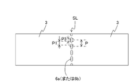
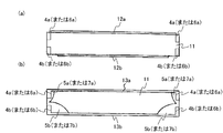
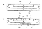
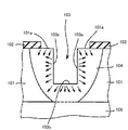
- a line having a predetermined depth from the surface of the N-type silicon substrate 101 is formed on a portion corresponding to the isolation region of the N-type silicon substrate 101, for example, on the scribe line SL by dicing or etching.
- the groove 103 is line-etched to reduce a margin for stress, and vibration during substrate transportation is formed.
- wafer cracks occur in the manufacturing process due to stress on the film.
- the groove processing is performed only in one direction only on the substrate surface, there is a limit to further reducing the diffusion time for forming the isolation region for element isolation, which is not suitable for a thick wafer.
Landscapes
- Element Separation (AREA)
- Thyristors (AREA)
- Dicing (AREA)
Abstract
Priority Applications (3)
| Application Number | Priority Date | Filing Date | Title |
|---|---|---|---|
| JP2015530675A JP6111335B2 (ja) | 2013-08-08 | 2014-06-26 | 半導体素子基板およびその製造方法 |
| US14/906,006 US20160148875A1 (en) | 2013-08-08 | 2014-06-26 | Semiconductor element substrate, and method for producing same |
| CN201480044667.XA CN105453250A (zh) | 2013-08-08 | 2014-06-26 | 半导体元件衬底及其制造方法 |
Applications Claiming Priority (2)
| Application Number | Priority Date | Filing Date | Title |
|---|---|---|---|
| JP2013-165615 | 2013-08-08 | ||
| JP2013165615 | 2013-08-08 |
Publications (1)
| Publication Number | Publication Date |
|---|---|
| WO2015019540A1 true WO2015019540A1 (fr) | 2015-02-12 |
Family
ID=52460903
Family Applications (1)
| Application Number | Title | Priority Date | Filing Date |
|---|---|---|---|
| PCT/JP2014/003426 Ceased WO2015019540A1 (fr) | 2013-08-08 | 2014-06-26 | Substrat d'élément semi-conducteur et son procédé de production |
Country Status (4)
| Country | Link |
|---|---|
| US (1) | US20160148875A1 (fr) |
| JP (1) | JP6111335B2 (fr) |
| CN (1) | CN105453250A (fr) |
| WO (1) | WO2015019540A1 (fr) |
Cited By (2)
| Publication number | Priority date | Publication date | Assignee | Title |
|---|---|---|---|---|
| EP3142143A1 (fr) * | 2015-09-11 | 2017-03-15 | ABB Technology AG | Procédé de fabrication d'un dispositif de puissance à semi-conducteur |
| US11398572B2 (en) | 2017-09-08 | 2022-07-26 | Hamamatsu Photonics K.K. | Semiconductor wafer manufacturing method, method of manufacturing semiconductor energy beam detecting element, and semiconductor wafer |
Families Citing this family (2)
| Publication number | Priority date | Publication date | Assignee | Title |
|---|---|---|---|---|
| JP7142606B2 (ja) * | 2019-06-04 | 2022-09-27 | 三菱電機株式会社 | 半導体装置 |
| CN115621122B (zh) * | 2021-07-14 | 2025-11-14 | 长鑫存储技术有限公司 | 半导体器件形成阵列圆形孔的制备方法 |
Citations (4)
| Publication number | Priority date | Publication date | Assignee | Title |
|---|---|---|---|---|
| JPH07235660A (ja) * | 1992-09-30 | 1995-09-05 | Rohm Co Ltd | サイリスタの製造方法 |
| JP2001185727A (ja) * | 1999-10-15 | 2001-07-06 | Fuji Electric Co Ltd | 半導体装置およびその製造方法 |
| JP2006164997A (ja) * | 2004-12-02 | 2006-06-22 | Toyota Motor Corp | 半導体装置の製造方法 |
| JP2012004174A (ja) * | 2010-06-14 | 2012-01-05 | Fuji Electric Co Ltd | 逆阻止型絶縁ゲート形バイポーラトランジスタおよびその製造方法 |
Family Cites Families (56)
| Publication number | Priority date | Publication date | Assignee | Title |
|---|---|---|---|---|
| US3365794A (en) * | 1964-05-15 | 1968-01-30 | Transitron Electronic Corp | Semiconducting device |
| US3458781A (en) * | 1966-07-18 | 1969-07-29 | Unitrode Corp | High-voltage planar semiconductor devices |
| US3535774A (en) * | 1968-07-09 | 1970-10-27 | Rca Corp | Method of fabricating semiconductor devices |
| US3612959A (en) * | 1969-01-31 | 1971-10-12 | Unitrode Corp | Planar zener diodes having uniform junction breakdown characteristics |
| US3628107A (en) * | 1969-05-05 | 1971-12-14 | Gen Electric | Passivated semiconductor device with peripheral protective junction |
| US3608186A (en) * | 1969-10-30 | 1971-09-28 | Jearld L Hutson | Semiconductor device manufacture with junction passivation |
| US3664894A (en) * | 1970-02-24 | 1972-05-23 | Rca Corp | Method of manufacturing semiconductor devices having high planar junction breakdown voltage |
| JPS4974486A (fr) * | 1972-11-17 | 1974-07-18 | ||
| US3972113A (en) * | 1973-05-14 | 1976-08-03 | Mitsubishi Denki Kabushiki Kaisha | Process of producing semiconductor devices |
| DE2340128C3 (de) * | 1973-08-08 | 1982-08-12 | SEMIKRON Gesellschaft für Gleichrichterbau u. Elektronik mbH, 8500 Nürnberg | Halbleiterbauelement hoher Sperrfähigkeit |
| US3896477A (en) * | 1973-11-07 | 1975-07-22 | Jearld L Hutson | Multilayer semiconductor switching devices |
| US4063272A (en) * | 1975-11-26 | 1977-12-13 | General Electric Company | Semiconductor device and method of manufacture thereof |
| JPS52101967A (en) * | 1976-02-23 | 1977-08-26 | Agency Of Ind Science & Technol | Semiconductor device |
| JPS584814B2 (ja) * | 1976-04-27 | 1983-01-27 | 三菱電機株式会社 | 半導体装置 |
| DE2633324C2 (de) * | 1976-07-24 | 1983-09-15 | SEMIKRON Gesellschaft für Gleichrichterbau u. Elektronik mbH, 8500 Nürnberg | Verfahren zum Herstellen von Halbleiterbauelementen hoher Sperrspannungsbelastbarkeit |
| US4040877A (en) * | 1976-08-24 | 1977-08-09 | Westinghouse Electric Corporation | Method of making a transistor device |
| DE2730130C2 (de) * | 1976-09-14 | 1987-11-12 | Mitsubishi Denki K.K., Tokyo | Verfahren zum Herstellen von Halbleiterbauelementen |
| DE2753207C2 (de) * | 1976-11-30 | 1989-10-12 | Mitsubishi Denki K.K., Tokio/Tokyo | Verfahren zum Herstellen von Halbleiterbauelementen |
| US4137100A (en) * | 1977-10-26 | 1979-01-30 | Western Electric Company | Forming isolation and device regions due to enhanced diffusion of impurities in semiconductor material by laser |
| DE2751485A1 (de) * | 1977-11-18 | 1979-05-23 | Semikron Gleichrichterbau | Verfahren zum herstellen von halbleiterkoerpern mit definiertem, durch aetzen erzielten und mit einem glas abgedeckten randprofil |
| US4249962A (en) * | 1979-09-11 | 1981-02-10 | Western Electric Company, Inc. | Method of removing contaminating impurities from device areas in a semiconductor wafer |
| US4325182A (en) * | 1980-08-25 | 1982-04-20 | General Electric Company | Fast isolation diffusion |
| US4570173A (en) * | 1981-05-26 | 1986-02-11 | General Electric Company | High-aspect-ratio hollow diffused regions in a semiconductor body |
| US4681656A (en) * | 1983-02-22 | 1987-07-21 | Byrum James E | IC carrier system |
| DE3324551A1 (de) * | 1983-07-07 | 1985-01-17 | Wacker-Chemitronic Gesellschaft für Elektronik-Grundstoffe mbH, 8263 Burghausen | Verfahren zur kennzeichnung von halbleiteroberflaechen durch laserstrahlung |
| JPS6222451A (ja) * | 1985-07-22 | 1987-01-30 | Sharp Corp | 半導体基板のpn接合アイソレ−シヨン方法 |
| EP0238694B1 (fr) * | 1986-03-27 | 1992-01-29 | Ibm Deutschland Gmbh | Méthode de formation de marques d'alignement positionnées identiquement sur les côtés opposés d'une galette semi-conductrice |
| US4814296A (en) * | 1987-08-28 | 1989-03-21 | Xerox Corporation | Method of fabricating image sensor dies for use in assembling arrays |
| US5213994A (en) * | 1989-05-30 | 1993-05-25 | Motorola, Inc. | Method of making high voltage semiconductor device |
| US5000811A (en) * | 1989-11-22 | 1991-03-19 | Xerox Corporation | Precision buttable subunits via dicing |
| JP3496347B2 (ja) * | 1995-07-13 | 2004-02-09 | 株式会社デンソー | 半導体装置及びその製造方法 |
| DE19601261C1 (de) * | 1996-01-16 | 1997-04-10 | Itt Ind Gmbh Deutsche | Verfahren und Hilfsvorrichtung zum Herstellen von Halbleiterschaltungselementen |
| US5872046A (en) * | 1996-04-10 | 1999-02-16 | Texas Instruments Incorporated | Method of cleaning wafer after partial saw |
| KR100273704B1 (ko) * | 1997-12-20 | 2000-12-15 | 윤종용 | 반도체기판제조방법 |
| US6339251B2 (en) * | 1998-11-10 | 2002-01-15 | Samsung Electronics Co., Ltd | Wafer grooves for reducing semiconductor wafer warping |
| WO2003028072A1 (fr) * | 2001-09-20 | 2003-04-03 | Renesas Technology Corp. | Procede de fabrication de dispositif semi-conducteur |
| NL1019613C2 (nl) * | 2001-12-19 | 2003-06-20 | Micronit Microfluidics Bv | Werkwijze voor het verdelen van een substraat in een aantal individuele chipdelen. |
| KR100940530B1 (ko) * | 2003-01-17 | 2010-02-10 | 삼성전자주식회사 | 실리콘 광소자 제조방법 및 이에 의해 제조된 실리콘광소자 및 이를 적용한 화상 입력 및/또는 출력장치 |
| JP2003332270A (ja) * | 2002-05-15 | 2003-11-21 | Renesas Technology Corp | 半導体装置およびその製造方法 |
| CN1241253C (zh) * | 2002-06-24 | 2006-02-08 | 丰田合成株式会社 | 半导体元件的制造方法 |
| WO2004015764A2 (fr) * | 2002-08-08 | 2004-02-19 | Leedy Glenn J | Integration de systeme verticale |
| JP4579489B2 (ja) * | 2002-09-02 | 2010-11-10 | 新光電気工業株式会社 | 半導体チップ製造方法及び半導体チップ |
| WO2004105089A2 (fr) * | 2003-05-15 | 2004-12-02 | Pan Jit Americas, Inc. | Dispositif thyristor de protection contre les surtensions a faible capacite |
| JP4660224B2 (ja) * | 2004-03-30 | 2011-03-30 | 三洋電機株式会社 | 半導体レーザ装置 |
| JP4930322B2 (ja) * | 2006-11-10 | 2012-05-16 | ソニー株式会社 | 半導体発光素子、光ピックアップ装置および情報記録再生装置 |
| US8629532B2 (en) * | 2007-05-08 | 2014-01-14 | Taiwan Semiconductor Manufacturing Co., Ltd. | Semiconductor wafer with assisting dicing structure and dicing method thereof |
| US7888236B2 (en) * | 2007-05-14 | 2011-02-15 | Taiwan Semiconductor Manufacturing Co., Ltd. | Semiconductor device and fabrication methods thereof |
| CN102037563B (zh) * | 2008-05-13 | 2013-06-05 | 富士电机株式会社 | 半导体器件及其制造方法 |
| US8064492B2 (en) * | 2009-01-26 | 2011-11-22 | Sanyo Electric Co., Ltd. | Method of manufacturing semiconductor laser device, semiconductor laser device and light apparatus |
| JP5560931B2 (ja) * | 2010-06-14 | 2014-07-30 | 富士電機株式会社 | 超接合半導体装置の製造方法 |
| US8361884B2 (en) * | 2010-06-22 | 2013-01-29 | Infineon Technologies Ag | Plasma dicing and semiconductor devices formed thereof |
| CN102244093B (zh) * | 2011-07-28 | 2013-09-25 | 江苏捷捷微电子股份有限公司 | 一种降低对通隔离扩散横向扩散宽度的结构及方法 |
| JP5803457B2 (ja) * | 2011-09-08 | 2015-11-04 | 三菱電機株式会社 | レーザダイオード素子の製造方法 |
| JP2013108111A (ja) * | 2011-11-18 | 2013-06-06 | Tokyo Electron Ltd | 基板の処理方法及びテンプレート |
| FR2987698B1 (fr) * | 2012-03-02 | 2014-04-04 | St Microelectronics Tours Sas | Composant de puissance vertical |
| JP6142496B2 (ja) * | 2012-10-12 | 2017-06-07 | 富士電機株式会社 | 半導体装置の製造方法 |
-
2014
- 2014-06-26 CN CN201480044667.XA patent/CN105453250A/zh active Pending
- 2014-06-26 WO PCT/JP2014/003426 patent/WO2015019540A1/fr not_active Ceased
- 2014-06-26 JP JP2015530675A patent/JP6111335B2/ja not_active Expired - Fee Related
- 2014-06-26 US US14/906,006 patent/US20160148875A1/en not_active Abandoned
Patent Citations (4)
| Publication number | Priority date | Publication date | Assignee | Title |
|---|---|---|---|---|
| JPH07235660A (ja) * | 1992-09-30 | 1995-09-05 | Rohm Co Ltd | サイリスタの製造方法 |
| JP2001185727A (ja) * | 1999-10-15 | 2001-07-06 | Fuji Electric Co Ltd | 半導体装置およびその製造方法 |
| JP2006164997A (ja) * | 2004-12-02 | 2006-06-22 | Toyota Motor Corp | 半導体装置の製造方法 |
| JP2012004174A (ja) * | 2010-06-14 | 2012-01-05 | Fuji Electric Co Ltd | 逆阻止型絶縁ゲート形バイポーラトランジスタおよびその製造方法 |
Cited By (2)
| Publication number | Priority date | Publication date | Assignee | Title |
|---|---|---|---|---|
| EP3142143A1 (fr) * | 2015-09-11 | 2017-03-15 | ABB Technology AG | Procédé de fabrication d'un dispositif de puissance à semi-conducteur |
| US11398572B2 (en) | 2017-09-08 | 2022-07-26 | Hamamatsu Photonics K.K. | Semiconductor wafer manufacturing method, method of manufacturing semiconductor energy beam detecting element, and semiconductor wafer |
Also Published As
| Publication number | Publication date |
|---|---|
| JPWO2015019540A1 (ja) | 2017-03-02 |
| CN105453250A (zh) | 2016-03-30 |
| US20160148875A1 (en) | 2016-05-26 |
| JP6111335B2 (ja) | 2017-04-05 |
Similar Documents
| Publication | Publication Date | Title |
|---|---|---|
| CN101414553B (zh) | 半导体晶片的制造方法 | |
| CN107833921B (zh) | 开关器件和制造开关器件的方法 | |
| JP6111335B2 (ja) | 半導体素子基板およびその製造方法 | |
| CN105321824B (zh) | 半导体装置的制造方法 | |
| US20170047316A1 (en) | Semiconductor device | |
| CN104756233A (zh) | 半导体器件的制造方法 | |
| US9178055B2 (en) | Semiconductor device | |
| CN109872974A (zh) | 具有集成pn二极管温度传感器的半导体器件 | |
| KR102881646B1 (ko) | 반도체 소자 및 그의 제조 방법 | |
| JP2015230920A (ja) | 半導体装置 | |
| JP4873002B2 (ja) | 半導体装置の製造方法 | |
| JP6623824B2 (ja) | 半導体装置およびその製造方法 | |
| JP2016086002A (ja) | 半導体装置及びその製造方法 | |
| JP5073933B2 (ja) | 半導体装置及びその製造方法 | |
| JP5636751B2 (ja) | 逆阻止型絶縁ゲート形バイポーラトランジスタおよびその製造方法 | |
| CN102222619B (zh) | 半导体装置的制造方法 | |
| JP7009933B2 (ja) | 半導体装置 | |
| JP2022178412A (ja) | 半導体装置及び半導体装置の製造方法 | |
| JP2014086431A (ja) | 半導体装置及びその製造方法 | |
| WO2014203881A1 (fr) | Procédé de fabrication d'élément de semi-conducteur au carbure de silicium | |
| JP5191109B2 (ja) | 接合型電界効果トランジスタ | |
| JP4260777B2 (ja) | 半導体装置及びその製造方法 | |
| JP2007180243A (ja) | 半導体装置及びその製造方法 | |
| CN100521244C (zh) | 结型场效应晶体管的制造方法 | |
| JP2018206870A (ja) | 半導体素子及びその製造方法 |
Legal Events
| Date | Code | Title | Description |
|---|---|---|---|
| WWE | Wipo information: entry into national phase |
Ref document number: 201480044667.X Country of ref document: CN |
|
| 121 | Ep: the epo has been informed by wipo that ep was designated in this application |
Ref document number: 14834387 Country of ref document: EP Kind code of ref document: A1 |
|
| ENP | Entry into the national phase |
Ref document number: 2015530675 Country of ref document: JP Kind code of ref document: A |
|
| WWE | Wipo information: entry into national phase |
Ref document number: 14906006 Country of ref document: US |
|
| NENP | Non-entry into the national phase |
Ref country code: DE |
|
| 122 | Ep: pct application non-entry in european phase |
Ref document number: 14834387 Country of ref document: EP Kind code of ref document: A1 |