WO2015033557A1 - 発光装置 - Google Patents
発光装置 Download PDFInfo
- Publication number
- WO2015033557A1 WO2015033557A1 PCT/JP2014/004513 JP2014004513W WO2015033557A1 WO 2015033557 A1 WO2015033557 A1 WO 2015033557A1 JP 2014004513 W JP2014004513 W JP 2014004513W WO 2015033557 A1 WO2015033557 A1 WO 2015033557A1
- Authority
- WO
- WIPO (PCT)
- Prior art keywords
- electrode
- light emitting
- emitting device
- led chip
- layer
- Prior art date
- Legal status (The legal status is an assumption and is not a legal conclusion. Google has not performed a legal analysis and makes no representation as to the accuracy of the status listed.)
- Ceased
Links
Images












Classifications
-
- H—ELECTRICITY
- H10—SEMICONDUCTOR DEVICES; ELECTRIC SOLID-STATE DEVICES NOT OTHERWISE PROVIDED FOR
- H10H—INORGANIC LIGHT-EMITTING SEMICONDUCTOR DEVICES HAVING POTENTIAL BARRIERS
- H10H20/00—Individual inorganic light-emitting semiconductor devices having potential barriers, e.g. light-emitting diodes [LED]
- H10H20/80—Constructional details
- H10H20/85—Packages
- H10H20/857—Interconnections, e.g. lead-frames, bond wires or solder balls
-
- H—ELECTRICITY
- H10—SEMICONDUCTOR DEVICES; ELECTRIC SOLID-STATE DEVICES NOT OTHERWISE PROVIDED FOR
- H10H—INORGANIC LIGHT-EMITTING SEMICONDUCTOR DEVICES HAVING POTENTIAL BARRIERS
- H10H20/00—Individual inorganic light-emitting semiconductor devices having potential barriers, e.g. light-emitting diodes [LED]
- H10H20/80—Constructional details
- H10H20/81—Bodies
- H10H20/819—Bodies characterised by their shape, e.g. curved or truncated substrates
- H10H20/82—Roughened surfaces, e.g. at the interface between epitaxial layers
-
- H—ELECTRICITY
- H10—SEMICONDUCTOR DEVICES; ELECTRIC SOLID-STATE DEVICES NOT OTHERWISE PROVIDED FOR
- H10H—INORGANIC LIGHT-EMITTING SEMICONDUCTOR DEVICES HAVING POTENTIAL BARRIERS
- H10H20/00—Individual inorganic light-emitting semiconductor devices having potential barriers, e.g. light-emitting diodes [LED]
- H10H20/80—Constructional details
- H10H20/83—Electrodes
- H10H20/831—Electrodes characterised by their shape
-
- H—ELECTRICITY
- H10—SEMICONDUCTOR DEVICES; ELECTRIC SOLID-STATE DEVICES NOT OTHERWISE PROVIDED FOR
- H10H—INORGANIC LIGHT-EMITTING SEMICONDUCTOR DEVICES HAVING POTENTIAL BARRIERS
- H10H20/00—Individual inorganic light-emitting semiconductor devices having potential barriers, e.g. light-emitting diodes [LED]
- H10H20/80—Constructional details
- H10H20/84—Coatings, e.g. passivation layers or antireflective coatings
-
- H—ELECTRICITY
- H10—SEMICONDUCTOR DEVICES; ELECTRIC SOLID-STATE DEVICES NOT OTHERWISE PROVIDED FOR
- H10H—INORGANIC LIGHT-EMITTING SEMICONDUCTOR DEVICES HAVING POTENTIAL BARRIERS
- H10H20/00—Individual inorganic light-emitting semiconductor devices having potential barriers, e.g. light-emitting diodes [LED]
- H10H20/80—Constructional details
- H10H20/85—Packages
- H10H20/8506—Containers
-
- H—ELECTRICITY
- H10—SEMICONDUCTOR DEVICES; ELECTRIC SOLID-STATE DEVICES NOT OTHERWISE PROVIDED FOR
- H10W—GENERIC PACKAGES, INTERCONNECTIONS, CONNECTORS OR OTHER CONSTRUCTIONAL DETAILS OF DEVICES COVERED BY CLASS H10
- H10W72/00—Interconnections or connectors in packages
- H10W72/20—Bump connectors, e.g. solder bumps or copper pillars; Dummy bumps; Thermal bumps
-
- H—ELECTRICITY
- H10—SEMICONDUCTOR DEVICES; ELECTRIC SOLID-STATE DEVICES NOT OTHERWISE PROVIDED FOR
- H10H—INORGANIC LIGHT-EMITTING SEMICONDUCTOR DEVICES HAVING POTENTIAL BARRIERS
- H10H20/00—Individual inorganic light-emitting semiconductor devices having potential barriers, e.g. light-emitting diodes [LED]
- H10H20/01—Manufacture or treatment
- H10H20/036—Manufacture or treatment of packages
- H10H20/0364—Manufacture or treatment of packages of interconnections
-
- H—ELECTRICITY
- H10—SEMICONDUCTOR DEVICES; ELECTRIC SOLID-STATE DEVICES NOT OTHERWISE PROVIDED FOR
- H10H—INORGANIC LIGHT-EMITTING SEMICONDUCTOR DEVICES HAVING POTENTIAL BARRIERS
- H10H20/00—Individual inorganic light-emitting semiconductor devices having potential barriers, e.g. light-emitting diodes [LED]
- H10H20/80—Constructional details
- H10H20/81—Bodies
- H10H20/819—Bodies characterised by their shape, e.g. curved or truncated substrates
-
- H—ELECTRICITY
- H10—SEMICONDUCTOR DEVICES; ELECTRIC SOLID-STATE DEVICES NOT OTHERWISE PROVIDED FOR
- H10H—INORGANIC LIGHT-EMITTING SEMICONDUCTOR DEVICES HAVING POTENTIAL BARRIERS
- H10H20/00—Individual inorganic light-emitting semiconductor devices having potential barriers, e.g. light-emitting diodes [LED]
- H10H20/80—Constructional details
- H10H20/85—Packages
- H10H20/858—Means for heat extraction or cooling
- H10H20/8581—Means for heat extraction or cooling characterised by their material
Definitions
- the present invention relates to a light emitting device provided with an LED chip (light emitting diode chip).
- a light emitting device 100 having a configuration shown in FIG. 32 is known (Japanese Patent Application Publication No. 2010-199247).
- the light emitting device 100 includes an LED chip 101 and a mounting substrate 102 on which the LED chip 101 is mounted.
- the LED chip 101 has a laminated structure of an n-type nitride semiconductor layer 112, a nitride light emitting layer 113, and a p-type nitride semiconductor layer 114 on one surface side of the light transmitting substrate 111.
- an anode electrode 107 is formed on the side of the p-type nitride semiconductor layer 114 opposite to the side of the nitride light emitting layer 113.
- the cathode electrode 108 is formed on the side of the n-type nitride semiconductor layer 112 on which the nitride light emitting layer 113 is stacked.
- conductor patterns 127 and 128 are formed on one surface side of the insulating substrate 121.
- the anode electrode 107 is joined to the conductor pattern 127 via a plurality of bumps 137.
- the cathode electrode 108 is bonded to the conductor pattern 128 via one bump 138.
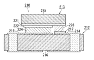
- an LED device (semiconductor light emitting device) 210 having a configuration shown in FIG. 33 is known (Japanese Patent Application Publication No. 2011-204838).
- the LED device 210 includes a circuit board 212 and an LED element 213 flip-chip mounted on the circuit board 212.
- a negative electrode 214 (first electrode) and a positive electrode 215 (second electrode) are formed.
- the LED element 213 includes a sapphire substrate 225, an n-type semiconductor layer 221 (first semiconductor layer), a light emitting layer (not shown), and a p-type semiconductor layer 222 (second semiconductor layer). Further, the LED element 213 includes an n-side bump 223 (first bump) connected to the n-type semiconductor layer 221 and a p-side bump 224 (second bump) connected to the p-type semiconductor layer 222. There is.
- the n-side bump 223 has a smaller planar area than the p-side bump 224.
- the n-side bump 223 and the p-side bump 224 are composed of an Au bump portion and a gold-tin eutectic layer.
- the n-side bump 223 and the p-side bump 224 have a thickness of 10 to 15 ⁇ m.
- the thickness of the gold-tin eutectic layer is 2 to 3 ⁇ m.
- a step difference of about 1 ⁇ m corresponding to the thickness of the p-type semiconductor layer 222 exists between the lower surface of each of the n-side bump 223 and the p-side bump 224.
- the n-side bump 223 and the p-side bump 224 of the LED element 213 are connected to the ⁇ electrode 214 and the + electrode 215 of the circuit board 212, respectively.
- a correction film 217 is formed in the connection region of the n-side bump 223 in the ⁇ electrode 214.
- the correction film 217 is formed to have a thickness (approximately 1 ⁇ m) substantially equal to the above-described step.
- the LED device 210 can reduce the amount of gold-tin alloy that protrudes from the connection region of the p-side bump 224. Further, in the bonding step of mounting the LED element 213 on the circuit board 212, the LED device 210 does not need to forcibly crush the p-side bump 224, so compared to the case where the correction film 217 is not provided, There is an advantage that the pressure can be reduced.
- the LED device 210 aligns the circuit board 212 and the LED element 213 in the bonding step at the time of manufacturing, and then applies pressure from the LED element 213 side, and heats from the circuit board 212 side to form an n-side bump It is necessary to melt the gold-tin eutectic layer of each of 223 and p-side bumps 224. Therefore, in the LED device 210, the thickness of each of the n-side bump 223 and the p-side bump 224 is likely to vary, and the thermal resistance is likely to vary.
- the present invention has been made in view of the above, and an object thereof is to provide a light emitting device capable of reducing the thermal resistance between the LED chip and the mounting substrate.
- the light emitting device of the present invention comprises a mounting substrate and an LED chip mounted on the mounting substrate.
- the mounting substrate includes a support, and a first conductor portion and a second conductor portion which are supported by the support and to which the LED chip is electrically connected.
- the LED chip includes a substrate, a first conductive type semiconductor layer formed on the first surface side of the substrate, and a second conductive type formed on the side of the first conductive type semiconductor layer opposite to the substrate side And a semiconductor layer.
- the LED chip is formed on a surface of the second conductive semiconductor layer, and a first electrode formed on the exposed surface of the first conductive semiconductor layer opposite to the substrate side. And a second electrode.
- the light emitting device protrudes from the surface side of the second conductive semiconductor layer to the surface side of the second conductor portion, contacts the surface of the second conductor portion, and extends along the outer periphery of the second electrode. It has a projection structure located.
- the first electrode and the first conductor portion are joined by a first joint portion formed of solder, and the second electrode and the second conductor portion are formed of solder. It joins by the 2nd junction part.
- the second bonding portion is formed to fill a space surrounded by the second electrode, the protrusion structure portion, and the second conductor portion.
- the projection structure is disposed along the outer periphery of the second electrode in plan view, and surrounds the second bonding portion.
- the mounting substrate has a height at which a portion where the projection structure overlaps with each other in a plan view is the same height as or lower than a portion joined to the second bonding portion in the second conductor portion.
- the light emitting device of the present invention can reduce the thermal resistance between the LED chip and the mounting substrate.
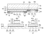
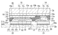
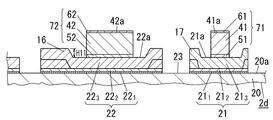
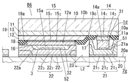
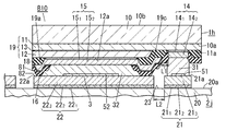
- FIG. 1 is a schematic cross-sectional view of the main part of the light emitting device of the first embodiment.
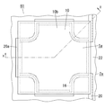
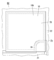
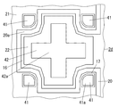
- FIG. 2 is a schematic plan view of relevant parts of the light emitting device of the first embodiment.
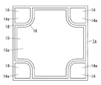
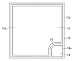
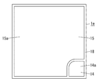
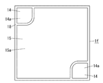
- FIG. 3 is a schematic plan view of the LED chip in the light emitting device of the first embodiment.
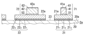
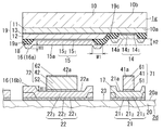
- FIG. 4 is an explanatory diagram of a method of manufacturing the light emitting device of the first embodiment.
- FIG. 5 is an explanatory drawing of the manufacturing method of the light emitting device of the first embodiment.
- FIG. 6 is an explanatory diagram of a method of manufacturing the light emitting device of the first embodiment.
- FIG. 7 is an explanatory drawing of the manufacturing method of the light emitting device of the first embodiment.
- FIG. 1 is a schematic cross-sectional view of the main part of the light emitting device of the first embodiment.
- FIG. 2 is a schematic plan view of relevant parts of the light emitting device of the first embodiment.
- FIG. 3 is a schematic plan view of the LED chip in
- FIG. 8 is a schematic cross-sectional view of main parts of a first modification of the light emitting device of the first embodiment.
- FIG. 9 is a schematic plan view of relevant parts of a second modification of the light emitting device of the first embodiment.
- FIG. 10 is a schematic plan view of an LED chip in a second modified example of the light emitting device of the first embodiment.
- FIG. 11 is an explanatory diagram of a manufacturing method of the second modified example of the light emitting device of the first embodiment.
- FIG. 12 is a schematic plan view of an LED chip in a third modification of the light emitting device of the first embodiment.
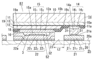
- FIG. 13 is a schematic cross-sectional view of main parts of the light emitting device of the second embodiment.
- FIG. 14 is a schematic plan view of the main part of the light emitting device of the second embodiment.
- FIG. 15 is a schematic plan view of the LED chip in the light emitting device of the second embodiment.
- FIG. 16 is an explanatory drawing of the manufacturing method of the light emitting device of the second embodiment.
- FIG. 17 is an explanatory drawing of the manufacturing method of the light emitting device of the second embodiment.
- FIG. 18 is an explanatory drawing of the manufacturing method of the light emitting device of the second embodiment.
- FIG. 19 is an explanatory drawing of the manufacturing method of the light emitting device of the embodiment 2;
- FIG. 20 is a schematic plan view of the main parts of a first modification of the light emitting device of the second embodiment.
- FIG. 21 is a schematic plan view of an LED chip in a first modified example of the light emitting device of the second embodiment.
- FIG. 22 is an explanatory drawing of the manufacturing method of the first modified example of the light emitting device of the embodiment 2;
- FIG. 23 is an explanatory diagram of a manufacturing method of the second modified example of the light emitting device of the second embodiment.
- FIG. 24 is a schematic plan view of an LED chip in a second modified example of the light emitting device of the second embodiment.
- FIG. 25 is a schematic cross-sectional view of main parts of a third modification of the light emitting device of the second embodiment.
- FIG. 26 is a schematic cross-sectional view of main parts of a fourth modified example of the light emitting device of the second embodiment.
- FIG. 27 is a schematic cross-sectional view of essential parts of a fifth modification of the light emitting device of the second embodiment.
- FIG. 28 is a schematic cross-sectional view of main parts of a sixth modification of the light emitting device of the second embodiment.
- FIG. 29 is an explanatory diagram of a manufacturing method of the sixth modified example of the light emitting device of the second embodiment.
- FIG. 30 is a schematic cross-sectional view of main parts of the light emitting device of the third embodiment.
- FIG. 31 is an explanatory drawing of the manufacturing method of the light emitting device of the third embodiment.
- FIG. 32 is a schematic cross-sectional view of a conventional light emitting device.
- FIG. 33 is a schematic cross-sectional view of a conventional LED device.
- FIG. 1 is a schematic, schematic cross-sectional view corresponding to the XX cross section of FIG.
- the light emitting device B1 includes a mounting substrate 2a and an LED chip 1a mounted on the mounting substrate 2a.
- the mounting substrate 2a includes a support 20, and a first conductor portion 21 and a second conductor portion 22 which are supported by the support 20 and to which the LED chip 1a is electrically connected.
- the LED chip 1 a includes a substrate 10, a first conductive semiconductor layer 11 formed on the first surface 10 a side of the substrate 10, and a first conductive semiconductor layer 11 formed on the opposite side of the substrate 10. And a second conductivity type semiconductor layer 12. Further, the LED chip 1 a is formed on the first electrode 14 formed on the exposed surface 11 a of the first conductive semiconductor layer 11 opposite to the substrate 10, and on the surface 12 a of the second conductive semiconductor layer 12.
- the light emitting device B1 protrudes from one side of the surface 12a of the second conductive semiconductor layer 12 to the other side of the surface 22a of the second conductor portion 22 and is in contact with the other side, along the outer periphery of the second electrode 15. And the projection structure part 16 located. More specifically, the light emitting device B1 protrudes from the surface 12a side of the second conductive type semiconductor layer 12 of the LED chip 1a to the surface 22a side of the second conductor portion 22 of the mounting substrate 2a to be a surface 22a of the second conductor portion 22. And a protrusion structure portion 16 located along the outer periphery of the second electrode 15.
- the first electrode 14 and the first conductor portion 21 are joined by the first joint portion 31 formed of solder, and the second electrode 15 and the second conductor portion 22 are formed of solder. It joins by the 2nd junction part 32 which was carried out.
- the second bonding portion 32 is formed so as to fill a space 3 surrounded by the second electrode 15, the protrusion structure portion 16, and the second conductor portion 22.
- the protrusion structure portion 16 is disposed along the outer periphery of the second electrode 15 and surrounds the second bonding portion 32 in a plan view.
- the mounting substrate 2a has a height at which the portion where the projection structure 16 overlaps in plan view is the same height as or lower than the position where the second conductor portion 22 is joined to the second bonding portion 32.
- the light emitting device B1 can make each of the first bonding portion 31 and the second bonding portion 32 thinner, and the first bonding portion 31 and the second bonding portion 32 each have the first conductor portion 21 and the second bonding portion 32. It becomes possible to join to each of 2 conductor parts 22 in a field.
- the light emitting device B1 can reduce the thermal resistance between the LED chip 1a and the mounting substrate 2a.
- the thickness control of the second bonding portion 32 can be performed by the protrusion structure portion 16, the accuracy of the thickness and size of the second bonding portion 32 can be enhanced, and the thermal resistance is reduced and the heat is reduced. It is possible to reduce the variation in resistance.
- the thickness of the second bonding portion 32 can be determined only by the thickness of the protrusion structure portion 16, and a protrusion is formed in a portion overlapping the protrusion structure portion 16 in the second conductor portion 22 of the mounting substrate 2a.
- the variation in the thermal resistance can be reduced.
- the light emitting device B1 can reduce the variation in the thermal resistance of each product. Thereby, the light emitting device B1 can improve the heat dissipation and the reliability.
- the “protruding structure portion 16 in plan view” means a shape in which the protruding structure portion 6 is viewed from the thickness direction of the protruding structure portion 6 along the thickness direction of the LED chip 1 a.
- the protrusion structure portion 16 is formed along the outer periphery of the second electrode 15 in the LED chip 1a, and protrudes on the surface 12a side of the second conductivity type semiconductor layer 12 more than the periphery of the protrusion structure portion 16 in the LED chip 1a. Is preferred. Thereby, in the light emitting device B1, the protrusion structure 16 is in contact with the surface 22a of the second conductor portion 22, and the second bonding portion 32 is surrounded by the second electrode 15, the protrusion structure 16 and the second conductor portion 22. Can be configured to fill the space 3.
- the mounting substrate 2a in the light emitting device B1 has the surface of the portion of the second conductor 22 overlapping the projection structure 16 flush with the surface of the portion of the second conductor 22 to be bonded to the second bonding portion 32.
- the thickness of the second bonding portion 32 can be determined only by the thickness of the protrusion structure portion 16, and in the portion overlapping the protrusion structure portion 16 in the second conductor portion 22 of the mounting substrate 2a.
- the variation in the thickness of the second bonding portion 32 can be further suppressed and the variation in the thermal resistance can be reduced as compared with the case where there is a protrusion.
- the light emitting device B1 can further increase the accuracy of the thickness and size of the second bonding portion 32, and can reduce the thermal resistance and the variation of the thermal resistance.
- the solder forming the first bonding portion 31 and the solder forming the second bonding portion 32 are preferably AuSn.
- the light emitting device B1 uses, for example, SnCuAg, which is a type of lead-free solder other than AuSn, as the solder for forming the first bonding portion 31 and the solder for forming the second bonding portion 32. Heat resistance can be improved. Therefore, for example, in the case of secondary mounting on a printed wiring board or the like, the light emitting device B1 can suppress remelting of the first bonding portion 31 and the second bonding portion 32 during secondary mounting. .
- the solder for forming the first bonding portion 31 and the solder for forming the second bonding portion 32 are not limited to AuSn, and may be, for example, AuSn, SnAgCu, AuGe, AuSi, PbSn or the like.
- the LED chip 1a and the mounting substrate 2a are prepared, and then the first step and the second step are sequentially performed.
- the first bonding portion 31 and the second bonding portion 32 are formed on the surface 21a side of the first conductor portion 21 of the mounting substrate 2a and on the surface 22a side of the second conductor portion 22.
- the first solder layer 41 and the second solder layer 42 which are the basis of each are formed.
- AuSn can be adopted, for example.
- the first solder layer 41 and the second solder layer 42 can be formed by, for example, a vapor deposition method or a plating method.
- the thicknesses of the first solder layer 41 and the second solder layer 42 are set to the same value.
- the area of the surface 41 a of the first solder layer 41 is set smaller than the area of the surface 14 a (see FIG. 3) of the first electrode 14.
- the area of the surface 42 a of the second solder layer 42 is set smaller than the area of the surface 15 a (see FIG. 3) of the second electrode 15.
- the thicknesses of the first solder layer 41 and the second solder layer 42 are determined by the protrusion amount H1 (see FIG. 6) of the protrusion structure 16 of the LED chip 1a and the second electrode 15 and the first electrode in the thickness direction of the LED chip 1a. It is set so as to be larger by a predetermined thickness ( ⁇ ) than the sum (H1 + H2) of the step H2 (see FIG. 6) with 14.
- the thicknesses of the first solder layer 41 and the second solder layer 42 are H1 + H2 + ⁇ .
- the thickness of the first solder layer 41 and the second solder layer 42 may be set to about 3 ⁇ m. In this case, ⁇ is 1 ⁇ m.
- the first solder layer 41 and the second solder layer 42 are preferably formed in the central portion of the region facing the first electrode 14 and the second electrode 15 in the mounting substrate 2a.
- the second solder layer 42 is disposed on the surface 22 a of the second conductor portion 22 so as to be located inside the vertical projection area of the projection structure 16 and away from the vertical projection area.
- the vertical projection area of the projection structure 16 means a projection area in the thickness direction of the projection structure 16. That is, the vertical projection area of the projection structure 16 means a vertical projection area in which the projection direction is along the thickness direction of the projection structure 16. In other words, the vertical projection area of the projection structure 16 means a vertical projection area on a plane orthogonal to the thickness direction of the projection structure 16.
- the first solder layer 41 and the second solder layer 42 have a smaller composition ratio of Au than the eutectic composition (70 at% Au, 30 at% Sn), and a composition that melts at a temperature of 300 ° C. or more and less than 400 ° C. (For example, 60 at% Au, 40 at% Sn) AuSn is preferable.
- the first solder layer 41 and the second solder layer 42 are not limited to AuSn, and are formed of a solder whose melting point is lower than that of the mounting substrate 2a and the LED chip 1a.
- the first barrier layer 51 and the second barrier layer 52 are respectively formed between the first conductor portion 21 and the second conductor portion 22 and the first solder layer 41 and the second solder layer 42.
- the first barrier layer 51 and the second barrier layer 52 diffuse the metal (for example, Sn or the like) between the first solder layer 41, the second solder layer 42 and the first conductor portion 21 and the second conductor portion 22.
- It is a layer which has a function of a diffusion barrier which suppresses that the composition of AuSn fluctuates due to As a material of the 1st barrier layer 51 and the 2nd barrier layer 52, although Pt can be adopted, for example, not only this but Pd etc. can also be adopted.
- the thicknesses of the first barrier layer 51 and the second barrier layer 52 are set to the same value.
- the thickness of the first barrier layer 51 and the second barrier layer 52 is preferably set to, for example, about 0.2 ⁇ m.
- the first barrier layer 51 and the second barrier layer 52 can be formed by, for example, a vapor deposition method or a plating method.
- first Au layer 61 and a second Au layer 62 on the first solder layer 41 and the second solder layer 42, respectively.
- first Au layer 61 and the second Au layer 62 are not shown.
- the first Au layer 61 and the second Au layer 62 are layers provided to suppress the oxidation of Sn in the first solder layer 41 and the second solder layer 42.
- the thicknesses of the first Au layer 61 and the second Au layer 62 are preferably sufficiently thinner than the thicknesses of the first solder layer 41 and the second solder layer 42, and for example, preferably 0.1 ⁇ m or less.
- the thickness of the first Au layer 61 and the second Au layer 62 is such that, when the first solder layer 41 and the second solder layer 42 are melted, Au is thermally diffused to the first solder layer 41 and the second solder layer 42. It is necessary to set so that the 1st conductor part 21, the 2nd conductor part 22, and the 1st electrode 14 and the 2nd electrode 15 may be joined.
- the thickness of each of the first Au layer 61 and the second Au layer 62 is preferably set, for example, in the range of about 0.05 ⁇ m to 0.1 ⁇ m.
- the first Au layer 61 and the second Au layer 62 can be formed by, for example, a vapor deposition method, a plating method, or the like.
- a laminated film of the first barrier layer 51, the first solder layer 41, and the first Au layer 61 is referred to as a first bonding layer 71, and the second barrier layer 52, the second solder layer 42, and the second Au layer 62.
- the laminated film of the above is referred to as a second bonding layer 72.
- the first bonding layer 71 may have at least the first solder layer 41, and is not limited to the laminated film, and may be a single layer film.
- the second bonding layer 72 only needs to include at least the second solder layer 42, and is not limited to the laminated film, and may be a single layer film.
- the die bonding apparatus includes, for example, a suction holder capable of holding the LED chip 1a by suction, a stage for mounting the mounting substrate 2a, a first heater provided on the stage and capable of heating the mounting substrate 2a, and a suction holder Or the thing of the structure provided with the 2nd heater attached to either of the holders holding an adsorption
- suction holder is preferable.
- a suction holder there is a collet or the like.
- the LED chip 1a and the mounting substrate 2a are opposed to each other.
- the first electrode 14 and the second electrode 15 of the LED chip 1a and the first conductor portion 21 and the second conductor portion 22 of the mounting substrate 2a are opposed to each other. This means that the LED chip 1a and the mounting substrate 2a are opposed to each other.
- the first electrode 14 and the second electrode 15 of the LED chip 1a adsorbed and held by the adsorption holder are made to face the first conductor portion 21 and the second conductor portion 22 of the mounting substrate 2a.
- the first electrode 14 and the second electrode 15 of the LED chip 1a, and the first conductor portion 21 and the second conductor portion 22 of the mounting substrate 2a are formed by the first joint portion 31 formed of solder and solder. It joins by the formed 2nd junction part 32.
- the first bonding portion 31 may include the first barrier layer 51 in addition to the portion formed by the solder as well as the case formed by only the solder.
- the second bonding portion 32 may include the second barrier layer 52 in addition to the portion formed by the solder as well as the case formed by only the solder.
- the first electrode 14 and the second electrode 15 of the LED chip 1a and the first bonding layer 71 and the second bonding layer 72 on the mounting substrate 2a are in contact with each other.
- the first solder layer 41 and the second solder layer 42 are melted while performing appropriate heating and pressure.
- Au diffuses from the first Au layer 61 into the melted solder, and the composition ratio of Au in the melted solder increases.
- the second solder layer 42 is melted, Au is diffused from the second Au layer 62 into the melted solder, and the composition ratio of Au in the melted solder increases.
- the second step after melting the first solder layer 41 and the second solder layer 42 as described above, pressure is applied from the LED chip 1 a side so that the projection structure 16 is in contact with the second conductor 22. Then, the molten solder is pushed down and spread laterally to fill the space 3 with solder and then it is solidified by cooling.
- the second step only heating of the mounting substrate 2a by the first heater may be performed, or heating of the LED chip 1a may be performed by the second heater attached to the collet or the holder holding the collet.
- the second step in consideration of the bonding between the mounting substrate 2a and the LED chip 1a, it is preferable to perform heating from both the first heater and the second heater.
- pressurization is performed by applying an appropriate load.
- the load is preferably set, for example, in a range of about 0.1 to 1 kg / cm 2 with respect to one LED chip 1a.
- the time for applying the load is preferably set, for example, in the range of about 0.1 to 1 second.
- the second step is preferably performed in an N 2 gas atmosphere or in a vacuum atmosphere.
- the melting temperature of the first solder layer 41 and the second solder layer 42 is preferably lower than the heat resistant temperature of the LED chip 1a.
- the composition ratio of Au should be the composition ratio near the eutectic composition, for example, the composition ratio of Au is 68 at% to 69 at%. If it exists, the melting temperature will be 300 ° C. or less.
- the composition of Au The ratio may be 56 at% or more and less than 70 at%.
- the volume of the second bonding layer 72 formed in the first step is set to be equal to the volume of the space 3 so that the solder forming the second bonding portion 32 does not go out of the space 3 .
- the melted solder is made such that the protrusion structure portion 16 of the LED chip 1a contacts the surface 22a of the second conductor portion 22 in a state where each of the first solder layer 41 and the second solder layer 42 is melted. Is pressed down to bond the LED chip 1a and the mounting substrate 2a. Therefore, in the method of manufacturing the light emitting device B1, it is possible to suppress the first electrode 14 and the first conductor portion 21 from becoming unbonded.
- the protrusion structure portion 16 is in contact with the second conductor portion 22, and the first electrode 14 and the first conductor portion 21 are joined by the first joint portion 31 formed of solder.
- the electrode 15 and the second conductor portion 22 are joined by the second joining portion 32 formed of solder.
- the second bonding portion 32 is formed to fill the space 3 surrounded by the second electrode 15, the protrusion structure portion 16, and the second conductor portion 22.
- the protrusion structure 16 causes the flow of the melted solder along the surface of the LED chip 1a. Suppress.
- the occurrence of a short circuit due to the solder between the first electrode 14 and the second electrode 15 can be suppressed.
- the second bonding layer 72 in the method of manufacturing the light emitting device B1, when the area of the second electrode 15 is larger than the area of the first electrode 14, there is a concern that unstable spread is more likely to occur in the second bonding portion 32 than in the first bonding portion 31. There is. Therefore, in the method of manufacturing the light emitting device B1, it is preferable to form the second bonding layer 72 in a predetermined pattern.
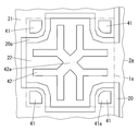
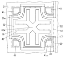
- the pattern of the second bonding layer 72 may be appropriately changed according to the planar shape of the second electrode 15. For example, as shown in FIGS. 5 and 7, it is preferable to use a radial shape that makes it difficult to take in air bubbles. .
- the entire front end surface of the projection structure 16 is in contact with the surface 22a of the second conductor 22.
- the entire surface of the end surface of the protrusion structure 16 is caused by the difference between the flatness of the end surface of the protrusion structure 16 and the flatness of the surface 22a of the second conductor 22. In some cases, it may be difficult to contact the surface 22 a of the second conductor portion 22.
- the light emitting device B1 may have a configuration in which the protrusion structure portion 16 partially contacts the surface 22a of the second conductor portion 22 as long as the parallelism of the LED chip 1a with respect to the mounting substrate 2a is within a desired range.
- the method of manufacturing the light emitting device B1 by increasing the load applied in the second step, it is possible to reduce the difference between the flatness of the tip end surface of the projection structure 16 and the flatness of the surface 22a of the second conductor 22. Thus, the contact area between the projection structure 16 and the second conductor 22 can be increased.
- the projection structure 16 when the projection structure 16 is formed of, for example, a metal, the projection structure 16 may be deformed so as to be compressed if the load applied in the second step is increased. As a result, the contact area between the projection structure 16 and the second conductor 22 can be increased.
- the first Au layer 61 and the second Au layer 62 on the first solder layer 41 and the second solder layer 42, respectively, in the first step.
- the bondability can be evaluated, for example, by die shear strength.
- the die shear strength is a force necessary to push the LED chip 1a, which is a die bonded to the mounting substrate 2a, parallel to the bonding surface.
- the die shear strength can be measured, for example, by a die shear tester or the like.
- the manufacturing becomes easier as compared to the case where the first bonding layer 71 and the second bonding layer 72 are formed on the LED chip 1a side.
- the components of the light emitting device B1 will be described in detail below.
- the mounting substrate 2a is a substrate on which the LED chip 1a is mounted. "Mounting” is a concept including arranging and mechanically connecting and electrically connecting the LED chips 1a. For this reason, the mounting substrate 2a has a function of mechanically holding the LED chip 1a and a function of forming a wire for supplying power to the LED chip 1a.
- the mounting substrate 2 a includes a first conductor portion 21 and a second conductor portion 22 as wiring.
- the mounting substrate 2a is configured to be able to mount one LED chip 1a.
- the mounting substrate 2a does not specifically limit the number of mountable LED chips 1a.
- the mounting substrate 2a may be configured to be able to mount a plurality of LED chips 1a.
- the light emitting device B1 may have a configuration in which a plurality of LED chips 1a are connected in series, may have a configuration in which they are connected in parallel, or may have a configuration in which they are connected in series and parallel. .
- the mounting substrate 2 a is configured such that the surface 21 a of the first conductor portion 21 and the surface 22 a of the second conductor portion 22 are aligned on one plane.
- the support 20 has a function of supporting the first conductor portion 21 and the second conductor portion 22 and a function of electrically insulating the first conductor portion 21 and the second conductor portion 22.
- the support 20 preferably has a function as a heat sink for efficiently transferring the heat generated in the LED chip 1 a to the outside. Therefore, the support 20 is preferably made of a material having high thermal conductivity.
- the support 20 can be made of, for example, an aluminum nitride substrate.
- the support 20 is not limited to the aluminum nitride substrate, but may be, for example, a sapphire substrate, a silicon carbide substrate, or the like.
- the support 20 may have a configuration in which an electrical insulating layer is formed on the surface of a silicon substrate, or may have a configuration in which an electrical insulating layer made of an appropriate material is formed on the surface of a metal plate.
- the material of the metal plate is preferably a metal having a high thermal conductivity.
- a material of the metal plate for example, copper, aluminum, silver, iron, aluminum alloy, phosphor bronze, copper alloy, nickel alloy, Kovar, etc. can be adopted.
- SiO 2 , Si 3 N 4 or the like can be adopted as the material of the electrical insulating layer formed on the surface of the silicon substrate.
- the support 20 is formed in a flat plate shape, and the first conductor portion 21 and the second conductor portion 22 are formed on the first surface 20a orthogonal to the thickness direction of the support 20.
- the thickness of the first conductor portion 21 and the thickness of the second conductor portion 22 are set to the same value.
- the shape of the support 20 is not limited to a flat plate, and for example, a recess for housing the LED chip 1a may be formed on one surface.
- the first conductor is formed on the inner bottom surface of the recess.
- the portion 21 and the second conductor portion 22 may be formed.
- the outer peripheral shape of the support 20 is rectangular.
- the outer peripheral shape of the support 20 is not limited to a rectangular shape, and may be, for example, a polygonal shape other than a rectangular shape, a circular shape, or the like.
- the first conductor portion 21 is a conductive layer to which the first electrode 14 of the LED chip 1a is electrically connected.
- the second conductor portion 22 is a conductive layer to which the second electrode 15 of the LED chip 1a is electrically connected.
- the first conductor section 21 and the second conductor part 22, for example, can be constituted by a laminated film of a Ti film 21 1, 22 1 and the Pt film 21 2, 22 2 and the Au film 21 3, 22 3.
- the first conductor portion 21 and the second conductor portion 22 are not limited thereto, for example, a laminated film of an Al film, a Ni film, a Pd film and an Au film, a laminated film of a Ni film and an Au film, a Cu film and a Ni film.
- a laminated film of a film and an Au film can be employed.
- the uppermost layer farthest from the support 20 is formed of Au, and the lowermost layer closest to the support 20 is in close contact with the support 20 It is preferable that it is formed of a highly elastic material.
- the first conductor portion 21 and the second conductor portion 22 are not limited to the laminated film, and may be formed of a single layer film.
- the mounting substrate 2a is formed with the first conductor portion 21 and the second conductor portion 22 such that the first conductor portion 21 and the second conductor portion 22 are spatially separated.
- the groove 23 is formed between the first conductor portion 21 and the second conductor portion 22 in the mounting substrate 2 a.
- the inner surface of the groove 23 is formed of a part of the first surface 20 a of the support 20 and the opposing surfaces of the first conductor portion 21 and the second conductor portion 22.
- the first conductor portion 21 and the second conductor portion 22 are formed on the first surface 20 a of the support 20 with the same thickness.
- the mounting substrate 2 a is configured such that the surface 21 a of the first conductor portion 21 and the surface 22 a of the second conductor portion 22 are aligned on one plane.
- the planar size of the mounting substrate 2a is preferably larger than the chip size of the LED chip 1a.
- the chip size of the LED chip 1a is not particularly limited.
- the chip size is 0.4 mm ⁇ (0.4 mm ⁇ 0.4 mm) or 0.6 mm ⁇ (0.6 mm ⁇ 0.6 mm) or 0.8 mm ⁇ (0.8 mm ⁇ 0. 0).
- the thing of 8 mm) or 1 mm ⁇ (1 mm ⁇ 1 mm) can be used.
- the planar shape of the LED chip 1a is not limited to the square shape, and may be, for example, a rectangular shape. When the planar shape of the LED chip 1a is rectangular, for example, a chip with a chip size of 0.5 mm ⁇ 0.24 mm can be used as the LED chip 1a.
- the first electrode 14 and the second electrode 15 are provided on one side in the thickness direction of the LED chip 1a.
- the LED chip 1a can be flip chip mounted on the mounting substrate 2a.
- the first conductive semiconductor layer 11 and the second conductive semiconductor layer 12 are formed in order from the side closer to the first surface 10a.
- the LED chip 1 a includes the semiconductor multilayer film 19 including the first conductive semiconductor layer 11 and the second conductive semiconductor layer 12.
- the first conductive semiconductor layer 11 is formed of an n-type semiconductor layer
- the second conductive semiconductor layer 12 is formed of a p-type semiconductor layer.
- the first conductive semiconductor layer 11 may be formed of a p-type semiconductor layer
- the second conductive semiconductor layer 12 may be formed of an n-type semiconductor layer.
- the substrate 10 has a function of supporting the semiconductor multilayer film 19.
- the semiconductor multilayer film 19 can be formed by an epitaxial growth method.
- Epitaxial growth methods include, for example, crystals such as metal organic vapor phase epitaxy (MOVPE), hydride vapor phase epitaxy (HVPE), molecular beam epitaxy (MBE), etc.
- the growth method can be adopted.
- the semiconductor multilayer film 19 may have impurities such as hydrogen, carbon, oxygen, silicon, iron and the like which are inevitably mixed in forming the semiconductor multilayer film 19.
- the substrate 10 can be configured of a crystal growth substrate when forming the semiconductor multilayer film 19.
- the LED chip 1a is composed of a blue LED chip that emits blue light.
- a GaN substrate can be adopted as the substrate 10, for example.
- the substrate 10 may be a substrate formed of a material capable of efficiently transmitting light emitted from the semiconductor multilayer film 19, and is not limited to a GaN substrate, and for example, a sapphire substrate or the like can be adopted.
- the substrate 10 is preferably a substrate transparent to the light emitted from the semiconductor multilayer film 19.
- the first conductive semiconductor layer 11 and the second conductive semiconductor layer 12 are formed on the first surface 10 a side of the substrate 10.
- the second surface 10b of the substrate 10 preferably constitutes a light extraction surface.
- the LED chip 1 a may have a configuration in which the semiconductor multilayer film 19 includes a buffer layer (not shown) between the substrate 10 and the first conductive semiconductor layer 11.
- the LED chip 1 a does not particularly limit the material and the emission color of the semiconductor multilayer film 19. That is, the LED chip 1a is not limited to the blue LED chip, but may be, for example, a purple LED chip, an ultraviolet LED chip, a red LED chip, a green LED chip, or the like.
- the semiconductor multilayer film 19 preferably includes the light emitting layer 13 between the first conductive semiconductor layer 11 and the second conductive semiconductor layer 12.
- the light emitted from the semiconductor multilayer film 19 is the light emitted from the light emitting layer 13, and the light emission wavelength is defined by the material of the light emitting layer 13.
- the light emitting layer 13 preferably has a single quantum well structure or a multiple quantum well structure, but is not limited thereto.
- a double heterostructure may be configured by the first conductive semiconductor layer 11, the light emitting layer 13, and the second conductive semiconductor layer 12.
- the first conductive semiconductor layer 11 is not limited to a single layer structure, and may have a multilayer structure.
- the second conductive semiconductor layer 12 is not limited to a single layer structure, and may have a multilayer structure.
- the second conductivity type semiconductor layer 12 can have, for example, a multilayer structure configured of a p-type electron block layer, a p-type semiconductor layer, and a p-type contact layer.
- the p-type semiconductor layer is a layer for transporting holes to the light emitting layer 13.
- the p-type electron blocking layer is a layer for suppressing an electron that has not been recombined with the hole in the light emitting layer 13 from leaking (overflowing) to the p-type semiconductor layer side.
- the p-type electron blocking layer is preferably set to have a higher band gap energy than the p-type semiconductor layer and the light emitting layer.
- the p-type contact layer is a layer provided to lower the contact resistance with the second electrode 15 and obtain a good ohmic contact with the second electrode 15.
- the p-type electron blocking layer and the p-type semiconductor layer can be composed of, for example, AlGaN layers having different compositions.
- the p-type contact layer can be formed of, for example, a p-type GaN layer.
- the LED chip 1a is removed by etching a part of the semiconductor multilayer film 19 from the surface 19a side of the semiconductor multilayer film 19 to the middle of the first conductive type semiconductor layer 11.
- the LED chip 1 a has a mesa structure formed by etching a part of the semiconductor multilayer film 19.
- a step is formed between the surface 12 a of the second conductive semiconductor layer 12 and the surface 11 a of the first conductive semiconductor layer 11.
- the first electrode 14 is formed on the exposed surface 11 a of the first conductive semiconductor layer 11
- the second electrode 15 is formed on the surface 12 a of the second conductive semiconductor layer 12. .
- the LED chip 1a When the conductivity type (first conductivity type) of the first conductivity type semiconductor layer 11 is n-type and the conductivity type (second conductivity type) of the second conductivity type semiconductor layer 12 is p-type, the LED chip 1a The first electrode 14 and the second electrode 15 constitute a negative electrode and a positive electrode, respectively. In the LED chip 1a, when the first conductivity type is p-type and the second conductivity type is n-type, the first electrode 14 and the second electrode 15 constitute a positive electrode and a negative electrode, respectively.
- the area of the surface 12a of the second conductive semiconductor layer 12 be larger than the area of the surface 11a of the first conductive semiconductor layer 11.
- the protrusion structure portion 16 is formed along the outer periphery of the second electrode 15 and protrudes on the surface 12 a side of the second conductive semiconductor layer 12.
- the second electrode 15 is larger than the first electrode 14, and the projection structure 16 is formed over the entire periphery of the outer periphery of the second electrode 15.
- the light emitting device B1 can further suppress the occurrence of a short circuit between the second electrode 15 and the first electrode 14 due to the solder forming the second bonding portion 32 at the time of manufacture.
- the light emitting device B1 can improve the reproducibility of the shape of the second bonding portion 32, and can reduce the variation in thermal resistance.
- the light emitting device B1 can manage the thickness of the second bonding portion 32 by the protrusion structure portion 16, the second electrode 15 and the second electrode 15 having a large heat dissipation area are not affected by the thickness of the first bonding portion 31. It is possible to increase the accuracy of the thickness and size of the second bonding portion 32 bonding the two conductor portions 22 and to reduce the thermal resistance and the variation of the thermal resistance.
- the projection structure 16 is preferably formed along the outer periphery of the second electrode 15, and the width W1 (see FIG. 6) is preferably constant.
- the light emitting device B1 can suppress the occurrence of a short circuit due to the solder between the second electrode 15 and the first electrode 14 while increasing the contact area between the second electrode 15 and the second conductivity type semiconductor layer 12. It becomes possible.
- the width W1 of the projection structure 16 is preferably set, for example, in the range of about 5 ⁇ m to 10 ⁇ m.
- the second electrode 15 is preferably formed so as to cover substantially the entire surface 12a of the second conductive semiconductor layer 12.
- the substantially entire surface 12 a of the second conductivity type semiconductor layer 12 is not limited to the entire surface 12 a.
- the LED chip 1a includes the insulating film 18 described later, and the outer peripheral portion of the surface 12a of the second conductive semiconductor layer 12 is covered by the insulating film 18, the LED chip 1a substantially covers the surface 12a of the second conductive semiconductor layer 12
- the entire surface means a portion of the surface 12 a of the second conductivity type semiconductor layer 12 which is not covered by the insulating film 18.
- the second electrode 15 is preferably formed to cover the surface 12a of the second conductive semiconductor layer 12 in a planar manner.
- the light emitting device B1 can improve the heat dissipation.
- the thickness of the first conductor portion 21 and the second conductor portion 22 be larger than the distance between the second electrode 15 and the second conductor portion 22.
- the distance between the second electrode 15 and the second conductor portion 22 means the distance between the central portion of the surface 15 a (see FIG. 6) of the second electrode 15 and the surface 22 a of the second conductor portion 22.
- the distance between the second electrode 15 and the second conductor portion 22 can be determined by the protrusion amount H1 of the protrusion structure portion 16. In other words, the distance between the second electrode 15 and the second conductor portion 22 is substantially the same as the protrusion amount H1 of the protrusion structure portion 16.
- the side surface of the second conductor portion 22 can function as a solder guiding portion for guiding the protruding solder toward the first surface 20a side of the support 20 at the time of manufacture.
- the light emitting device B1 can suppress the occurrence of a short circuit between the second electrode 15 and the first electrode 14 due to the solder protruding from the space 3.
- the first surface 20 a of the support 20 preferably has lower solder wettability than the side surfaces of the first conductor portion 21 and the second conductor portion 22.
- the LED chip 1a preferably includes the insulating film 18 formed on the surface 12a of the second conductive semiconductor layer 12 so as to surround the contact region of the second electrode 15 with the second conductive semiconductor layer 12 .
- the second electrode 15 is formed across the surface 12 a of the second conductive semiconductor layer 12 and the surface of the insulating film 18, and the second conductive semiconductor of the second electrode 15 than the central portion
- the outer peripheral portion protruding in the direction away from the layer 12 doubles as the projection structure 16.
- the insulating film 18 is a silicon oxide film.
- the insulating film 18 may be an electrical insulating film. Therefore, the material of the insulating film 18 may be any material having electrical insulation, and is not limited to SiO 2 , and, for example, Si 3 N 4 , Al 2 O 3 , TiO 2 , Ta 2 O 5 , ZrO 2 , Y 2 O 3 , CeO 2 , Nb 2 O 5 or the like can be employed.
- the thickness of the insulating film 18 is set to, for example, 1 ⁇ m, but is not particularly limited.
- the insulating film 18 can be formed by, for example, a chemical vapor deposition (CVD) method, a vapor deposition method, a sputtering method, or the like.
- the insulating film 18 is not limited to a single layer film, and may be a multilayer film.
- the multilayer film provided as the insulating film 18 may be formed of a dielectric multilayer film for reflecting light generated in the semiconductor multilayer film 19.
- the insulating film 18 is formed across the surface 19a of the mesa structure (the surface 12a of the second conductivity type semiconductor layer 12), the side surface 19c, and the surface 11a of the first conductivity type semiconductor layer 11. Is preferred.
- the portion of the insulating film 18 formed on the surface 11 a of the first conductive semiconductor layer 11 is formed in a pattern surrounding the contact region of the first electrode 14 with the first conductive semiconductor layer 11. Is preferred.
- the insulating film 18 preferably has a function as a passivation film (passivation film) for protecting the function of the semiconductor multilayer film 19, and SiO 2 or Si 3 N 4 is preferable as the material thereof.
- the light emitting device B1 can improve the reliability.
- the contact between the first electrode 14, the second electrode 15, and the first conductive semiconductor layer 11 and the second conductive semiconductor layer 12 be an ohmic contact.
- Ohmic contact means that there is no rectification of the current generated due to the direction of applied voltage among the contacts of the first electrode 14 and the second electrode 15 with the first conductive semiconductor layer 11 and the second conductive semiconductor layer 12.
- the ohmic contact preferably has a substantially linear current-voltage characteristic, and more preferably a linear one. Also, the ohmic contact preferably has a lower contact resistance.
- the current passing through the interface between the first electrode 14 and the first conductivity type semiconductor layer 11 overcomes the Schottky barrier, and the shot current It is considered to be the sum of the tunnel current passing through the key barrier.
- the current passing through the interface between the second electrode 15 and the second conductivity type semiconductor layer 12 overcomes the Schottky barrier and thermionic emission current and the Schottky It is considered to be the sum of the tunnel current passing through the barrier.
- an ohmic contact is approximately realized when the tunnel current is dominant. It is thought that
- the first electrode 14 includes an electrode layer (first connecting electrode layer) 14 1, the electrode layer (first pad electrode layer) includes a 14 2. Electrode layer 14 1 in order to obtain an ohmic contact with the first conductive semiconductor layer 11 is formed on the surface 11a of the first conductivity type semiconductor layer 11. Electrode layer 14 2, for bonding the mounting substrate 2a through a first joint portion 31 is formed so as to cover the electrode layer 14 1. Electrode layers 14 1, for example, can be formed by forming a film by vapor deposition or the like Al film on the surface 11a of the first conductivity type semiconductor layer 11. Electrode layer 14 2, for example, can be constituted by a laminated film of a Ti film and an Au film. Electrode layer 14 2, for example, can be formed by vapor deposition or the like. The first electrode 14 is not particularly limited to the layer structure, for example, the first electrode 14 may be composed of whole shape only by the electrode layer 14 1, and the electrode layer 14 1 and the electrode layer 14 2 May be provided with another electrode layer.
- the second electrode 15 includes the electrode layer (second connecting electrode layer) 15 1, and the electrode layer (second pad electrode layer) 15 2. Electrode layer 15 1 in order to obtain the second conductivity type semiconductor layer 12 and the ohmic contact is formed on the surface 12a of the second conductivity type semiconductor layer 12. Electrode layer 15 2, for bonding the mounting substrate 2a via the second joint portion 32 is formed so as to cover the electrode layer 15 1. Electrode layers 15 1, for example, can be formed by forming a film by vapor deposition or the like laminated film of Ni film and Ag film on the surface 12a of the second conductivity type semiconductor layer 12. Electrode layer 15 2, for example, can be constituted by a laminated film of a Ti film and an Au film.
- Electrode layer 15 2 can be formed by vapor deposition or the like.
- the second electrode 15 is not particularly limited to the layer structure, for example, the second electrode 15 may be composed of whole shape only by the electrode layer 15 1, and the electrode layer 15 1 and the electrode layer 15 2 May be provided with another electrode layer.
- Electrode layer 15 2 that are formed across the electrode layer 15 1 of the surface insulating film 18 surface of the preferred.
- an outer peripheral portion of the second electrode 15 which protrudes in a direction away from the second conductive semiconductor layer 12 more than the central portion also serves as the projection structure 16.
- the light emitting device B1 can increase the bonding area between the LED chip 1a and the mounting substrate 2a, thereby reducing the thermal resistance, and the heat generated by the semiconductor multilayer film 19 of the LED chip 1a It becomes easy to transmit to the mounting substrate 2 a side through the projection structure 16. Therefore, the light emitting device B1 can improve heat dissipation.
- the second bonding layer 72 (see FIGS. 4 and 6) has a larger amount of solder than the first bonding layer 71 (see FIGS. 4 and 6), and , The change in thickness in the second step is large.
- the second bonding layer 72 is more likely to depress the melted solder than the first bonding layer 71, and the thickness variation of the second bonding layer 72, etc. Because of this, the solder may protrude from the space 3.
- the distance L2 between the first conductor portion 21 and the second conductor portion 22 is preferably wider than the distance L1 between the first electrode 14 and the second electrode 15.
- the light emitting device B1 does not change the shapes of the first electrode 14 and the second electrode 15 of the LED chip 1a, and prevents the short circuit between the first electrode 14 and the second electrode 15 while the space 3 is formed. It becomes possible to absorb the solder which has run off from the grooves 23.
- the first conductor in the second conductor portion 22 is set such that the distance L2 between the first conductor portion 21 and the second conductor portion 22 is wider than the distance L1 between the first electrode 14 and the second electrode 15 It is preferable that the end on the side of the portion 21 be recessed from the end on the side of the first electrode 14 in the second electrode 15. Thereby, in the configuration in which the second electrode 15 of the LED chip 1a is larger than the first electrode 14, for example, the light emitting device B1 does not change the shapes of the first electrode 14 and the second electrode 15 of the LED chip 1a. It is possible to absorb the solder protruding from the space 3 by the groove 23 while preventing a short circuit between the first electrode 14 and the second electrode 15.
- the thickness of the first conductor portion 21 and the second conductor portion 22 is preferably larger than the distance between the second electrode 15 and the second conductor portion 22.
- the light emitting device B1 can further suppress the occurrence of a short circuit between the second electrode 15 and the first electrode 14 due to the solder that has come out of the space 3.
- the second bonding portion 32 preferably includes a second barrier layer 52 which is a barrier layer formed on the surface 22 a of the second conductor portion 22 in addition to the portion formed of the solder.
- the second barrier layer 52 has a function of a diffusion barrier.
- the second bonding portion 32 is preferably formed such that the second barrier layer 52 is separated from the protrusion structure 16 inside the protrusion structure 16.
- a portion formed of solder is a portion of the surface 22a of the second conductor portion 22 where the second barrier layer 52 is not formed, and the surface and the side surface of the second barrier layer 52. It is preferably formed to cover.
- the light emitting device B1 can suppress solder corrosion caused by the heat history in the mounting process, and stabilize the mechanical characteristics, the electrical characteristics, the chemical characteristics, and the like of the second bonding portion 32. As a result, the bonding reliability of the second bonding portion 32 can be improved.
- the LED chip 1a includes the insulating film 18 formed on the surface 12a of the second conductivity type semiconductor layer 12 so as to surround the contact region of the second electrode 15 with the second conductivity type semiconductor layer 12.
- the light emitting device B ⁇ b> 1 may be configured such that the insulating film 18 doubles as the protrusion structure 16 as a first modification.
- the thickness of the insulating film 18 may be set larger than the thickness of the second electrode 15.
- the structure of the LED chip 1a can be simplified and the manufacturing process can be simplified, and cost reduction can be achieved.
- the protrusion amount of the protrusion structure portion 16 can be a difference between the film thickness of the insulating film 18 and the thickness of the second electrode 15, so the protrusion structure portion 16 It is possible to improve the accuracy of the protrusion amount of
- FIG. 9 is a schematic plan view of a light emitting device B2 according to a second modification of the light emitting device B1 according to this embodiment.
- the light emitting device B2 has substantially the same basic configuration as the light emitting device B1.
- the shapes of the first electrode 14 and the second electrode 15 in the LED chip 1b see FIG. 10
- the shapes of the first conductor 21 and the second conductor 22 in the mounting substrate 2b see FIG. 11
- It is only different from the light emitting device B1. Therefore, detailed description of the light emitting device B2 is omitted.
- the same components as those of the light emitting device B1 are denoted by the same reference numerals.
- the LED chip 1 b is smaller in chip size than the LED chip 1 a (see FIGS. 1 and 3).
- the surface 11a of the first conductive type semiconductor layer 11 is exposed at each of the four corners of the semiconductor multilayer film 19, and the first electrode 14 is formed on each surface 11a.
- the LED chip 1 a includes four first electrodes 14.
- the surface 11a of the first conductive type semiconductor layer 11 is exposed at one of four corners of the semiconductor multilayer film 19, and the first electrode 14 is formed on the surface 11a. is there. Therefore, in the LED chip 1b, the shape of the second electrode 15 is different from that of the LED chip 1a.
- FIG. 12 is a schematic bottom view of an LED chip 1c in a third modification of the light emitting device B1 according to this embodiment.
- the third modification of the light emitting device B1 is different from the LED chip 1a in the shapes of the first electrode 14 and the second electrode 15 in the LED chip 1c.
- a mounting substrate (not shown) in which the shapes and the like of the first conductor portion 21 and the second conductor portion 22 in the mounting substrate 2a are changed In the point of providing the Therefore, the detailed description of the third modification of the light emitting device B1 will be omitted.
- the LED chip 1c is smaller in chip size than the LED chip 1a (see FIGS. 1 and 3) and larger than the LED chip 1b (see FIGS. 9 and 10).
- the surface 11a of the first conductivity type semiconductor layer 11 is exposed at two of four corners of the semiconductor multilayer film 19, and the first electrode 14 is formed on each surface 11a. Therefore, the LED chip 1c includes two first electrodes 14, and the shape of the second electrode 15 is different from that of the LED chips 1a and 1b.
- FIG. 13 is a schematic schematic cross-sectional view corresponding to the XX cross section of FIG.
- the same components as those of the light emitting device B1 of the first embodiment are denoted by the same reference numerals, and the description will be appropriately omitted.
- the light emitting device B3 includes a mounting substrate 2d and an LED chip 1d mounted on the mounting substrate 2d.
- the mounting substrate 2 d includes a support 20, and a first conductor portion 21 and a second conductor portion 22 which are supported by the support 20 and to which the LED chip 1 d is electrically connected.
- the LED chip 1 d includes a substrate 10, a first conductive semiconductor layer 11 formed on the first surface 10 a side of the substrate 10, and a first conductive semiconductor layer 11 formed on the opposite side to the substrate 10. And a second conductivity type semiconductor layer 12.
- the LED chip 1 d is formed on the first electrode 14 formed on the exposed surface 11 a of the first conductive semiconductor layer 11 opposite to the substrate 10 and on the surface 12 a of the second conductive semiconductor layer 12.
- the light emitting device B3 protrudes from one of the surface 12a side of the second conductive semiconductor layer 12 and the surface 22a of the second conductor portion 22 to the other side and is in contact with the other side, and along the outer periphery of the second electrode 15 And the projection structure part 16 located.
- the first electrode 14 and the first conductor portion 21 are joined by the first joint portion 31 formed of solder, and the second electrode 15 and the second conductor portion 22 are formed of solder. It joins by the 2nd junction part 32 which was carried out.
- the second bonding portion 32 is formed so as to fill a space 3 surrounded by the second electrode 15, the protrusion structure portion 16, and the second conductor portion 22.
- the protrusion structure portion 16 is disposed along the outer periphery of the second electrode 15 and surrounds the second bonding portion 32 in a plan view. Only the first bonding portion 31 is interposed between the LED chip 1 a and the first conductor portion 21. Therefore, the light emitting device B3 can make each of the first bonding portion 31 and the second bonding portion 32 thinner, and the first bonding portion 31 and the second bonding portion 32 respectively have the first conductor portion 21 and the second bonding portion 32. It becomes possible to join to each of 2 conductor parts 22 in a field. Thus, the light emitting device B3 can reduce the thermal resistance between the LED chip 1d and the mounting substrate 2d.
- the light emitting device B3 can manage the thickness of the second bonding portion 32 by the projection structure 16, accuracy in the thickness and size of the second bonding portion 32 can be improved, and the thermal resistance can be reduced and the heat can be reduced. It is possible to reduce the variation in resistance. In short, the light emitting device B3 can reduce the variation in the thermal resistance of each product. Thus, the light emitting device B3 can improve the heat dissipation and the reliability.
- the “protruding structure portion 16 in plan view” means a shape in which the protruding structure portion 6 is viewed from the thickness direction of the protruding structure portion 6 along the thickness direction of the LED chip 1 d.
- the protrusion structure portion 16 is formed in the second conductor portion 22 along the outer periphery of the second electrode 15, and protrudes on the surface 22a side of the second conductor portion 22 more than the periphery of the protrusion structure portion 16 in the mounting substrate 2d. Is preferred.
- the protrusion structure 16 is in contact with the surface 15a of the second electrode 15, and the second bonding portion 32 is surrounded by the second electrode 15, the protrusion structure 16, and the second conductor 22.
- the configuration can be such that the space 3 is filled.
- the LED chip 1d and the mounting substrate 2d are prepared, and then the first step and the second step are sequentially performed.
- a first bonding portion 31 and a second bonding portion 32 are provided on the surface 21a side of the first conductor portion 21 of the mounting substrate 2d and on the surface 22a side of the second conductor portion 22, a first bonding portion 31 and a second bonding portion 32 are provided.
- the first solder layer 41 and the second solder layer 42 which are the basis of each are formed.
- AuSn can be adopted, for example.
- the first solder layer 41 and the second solder layer 42 can be formed by, for example, a vapor deposition method or a plating method.
- the thicknesses of the first solder layer 41 and the second solder layer 42 are set to the same value.
- the area of the surface 41 a of the first solder layer 41 is set smaller than the area of the surface 14 a (see FIG. 15) of the first electrode 14.
- the area of the surface 42 a of the second solder layer 42 is set smaller than the area of the surface 15 a (see FIG. 15) of the second electrode 15.
- the thicknesses of the first solder layer 41 and the second solder layer 42 are determined by the amount H11 (see FIG. 18) of protrusion of the protrusion structure 16 from the surface 22a of the second conductor 22 and the second in the thickness direction of the LED chip 1d. It is set so as to be larger than the sum (H11 + H2) of the step H2 (see FIG. 18) between the electrode 15 and the first electrode 14 by a predetermined thickness ( ⁇ ).
- the thicknesses of the first solder layer 41 and the second solder layer 42 are H11 + H2 + ⁇ .
- the thicknesses of the first solder layer 41 and the second solder layer 42 may be set to about 3 ⁇ m. In this case, ⁇ is 1 ⁇ m.
- the first solder layer 41 and the second solder layer 42 are preferably formed in the central portion of the region facing the first electrode 14 and the second electrode 15 in the mounting substrate 2 d.
- the second solder layer 42 is disposed on the surface 22 a of the second conductor portion 22 so as to be positioned on the inner side of the projection structure 16 and away from the projection structure 16 in a plan view.
- the first barrier layer 51 and the second barrier layer 52 are respectively formed between the first conductor portion 21 and the second conductor portion 22 and the first solder layer 41 and the second solder layer 42. preferable.
- first step it is preferable to form a first Au layer 61 and a second Au layer 62 on the first solder layer 41 and the second solder layer 42, respectively.
- first bonding layer 71 a laminated film of the first barrier layer 51, the first solder layer 41, and the first Au layer 61
- second barrier layer 52, the second solder layer 42, and the second Au layer 62 a laminated film of the above is referred to as a second bonding layer 72.
- the first bonding layer 71 may have at least the first solder layer 41, and is not limited to the laminated film, and may be a single layer film.
- the second bonding layer 72 only needs to include at least the second solder layer 42, and is not limited to the laminated film, and may be a single layer film.
- the die bonding apparatus includes, for example, a suction holder capable of holding the LED chip 1d by suction, a stage for mounting the mounting substrate 2d, a first heater provided on the stage and capable of heating the mounting substrate 2d, and a suction holder Or the thing of the structure provided with the 2nd heater attached to either of the holders holding an adsorption
- suction holder is preferable.
- a suction holder there is a collet or the like.
- the LED chip 1d and the mounting substrate 2d are opposed to each other.
- the first electrode 14 and the second electrode 15 of the LED chip 1 d suctioned and held by the suction holder are made to face the first conductor portion 21 and the second conductor portion 22 of the mounting substrate 2 d.
- the first electrode 14 and the second electrode 15 of the LED chip 1 d and the first conductor portion 21 and the second conductor portion 22 of the mounting substrate 2 d are formed by the first joint portion 31 formed of solder and solder It joins by the formed 2nd junction part 32.
- the first electrode 14 and the second electrode 15 of the LED chip 1 d and the first bonding layer 71 and the second bonding layer 72 on the mounting substrate 2 d are in contact with each other in a superimposed state
- the first solder layer 41 and the second solder layer 42 are melted while performing appropriate heating and pressure.
- pressure is applied from the LED chip 1 d side so that the projection structure 16 is in contact with the second electrode 15.
- the molten solder is pushed down and spread laterally to fill the space 3 with solder and then it is solidified by cooling.
- the volume of the second bonding layer 72 formed in the first step is set to be equal to the volume of the space 3 so that the solder forming the second bonding portion 32 does not go out of the space 3 .
- the melted solder is made such that the protrusion structure 16 of the mounting substrate 2d contacts the surface 15a of the second electrode 15 in a state in which each of the first solder layer 41 and the second solder layer 42 is melted.
- the LED chip 1d and the mounting substrate 2d are bonded by pressing down. Therefore, in the method of manufacturing the light emitting device B3, it is possible to suppress the first electrode 14 and the first conductor portion 21 from becoming unbonded.
- the protrusion structure portion 16 is in contact with the second electrode 15, and the first electrode 14 and the first conductor portion 21 are joined by the first joint portion 31 formed of solder. 15 and the second conductor portion 22 are joined by the second joint portion 32 formed of solder.
- the second bonding portion 32 is formed so as to fill the space 3 surrounded by the second electrode 15, the protrusion structure portion 16, and the second conductor portion 22. It is possible to In the method of manufacturing the light emitting device B3, when the molten solder of the second bonding layer 72 is pushed down and spread in the lateral direction, the protrusion structure 16 causes the flow of the molten solder along the surface of the LED chip 1d.
- the second bonding layer 72 in a predetermined pattern.
- the pattern of the second bonding layer 72 may be appropriately changed according to the planar shape of the second electrode 15. For example, as shown in FIG. 17 and FIG. 19, it is preferable to use a radial shape that makes it difficult to take in air bubbles. .
- the manufacturing method of light-emitting device B3 it is preferable to apply a load so that the whole surface of the front-end
- the LED chip 1d is entirely covered with the tip surface of the protrusion structure 16 due to the difference between the flatness of the tip surface of the protrusion structure 16 and the flatness on the LED chip 1d side. Sometimes it is difficult to get in touch with the side. In the example of FIG.
- the light emitting device B3 may be configured such that the projection structure 16 partially contacts the surface 15a of the second electrode 15 as long as the parallelism of the LED chip 1d with respect to the mounting substrate 2d is within a desired range.
- the method of manufacturing the light emitting device B3 by increasing the load applied in the second step, it is possible to reduce the difference between the flatness of the tip end surface of the protrusion structure 16 and the flatness on the LED chip 1d side.
- the contact area between the portion 16 and the second electrode 15 can be increased.
- the projection structure 16 when the projection structure 16 is formed of, for example, a metal, the projection structure 16 can be deformed so as to be compressed if the load applied in the second step is increased. Become.
- the contact area between the projection structure 16 and the second electrode 15 can be increased.
- the first Au layer 61 and the second Au layer 62 on the first solder layer 41 and the second solder layer 42, respectively, in the first step.
- the method of manufacturing the light emitting device B3 it is possible to suppress the oxidation of Sn in the first solder layer 41 and the second solder layer 42 before the second step, and the LED chip 1d and the mounting substrate 2d It is possible to improve the bondability of the
- the protrusion structure 16 is formed on the LED chip 1a.
- the light emitting device B3 of the present embodiment is different in that the projection structure 16 is formed on the mounting substrate 2d.
- the mounting substrate 2 d is substantially the same as the mounting substrate 2 a in the light emitting device B 1 of the first embodiment, and is different in that the protrusion structure portion 16 is provided.
- the mounting substrate 2 d includes the support 20, the first conductor portion 21, the second conductor portion 22, and the protrusion structure portion 16.
- the mounting substrate 2 d is formed with the first conductor portion 21 and the second conductor portion 22 such that the first conductor portion 21 and the second conductor portion 22 are spatially separated.
- the groove 23 is formed between the first conductor portion 21 and the second conductor portion 22.
- the inner surface of the groove 23 is formed of a part of the first surface 20 a of the support 20 and the opposing surfaces of the first conductor portion 21 and the second conductor portion 22.
- the first conductor portion 21 and the second conductor portion 22 are formed on the first surface 20 a of the support 20 with the same thickness.
- the mounting substrate 2d is configured such that the surface 21a of the first conductor portion 21 and the surface 22a of the second conductor portion 22 are aligned on one plane.
- the protrusion structure portion 16 is formed in a shape along the outer periphery of the second electrode 15 in the second conductor portion 22, and protrudes on the surface 22 a side of the second conductor portion 22.
- the mounting substrate 2 d includes a protrusion structure portion 17 surrounding the first bonding portion 31. The protrusion structure portion 17 protrudes from the surface 21 a of the first conductor portion 21.
- the LED chip 1d has substantially the same configuration as the LED chip 1a (see FIGS. 1 and 3), and is different from the LED chip 1a in that the LED chip 1d does not include the protrusion structures 16 and 17. Although the LED chip 1d has the same chip size as the LED chip 1a, the present invention is not limited to this.
- the second electrode 15 is preferably larger than the first electrode 14.
- the projection structure portion 16 is preferably formed in a shape along the entire outer periphery of the second electrode 15 in the second conductor portion 22.
- the light emitting device B3 can further suppress the occurrence of a short circuit between the second electrode 15 and the first electrode 14 due to the solder forming the second bonding portion 32 at the time of manufacture.
- the light emitting device B3 can improve the reproducibility of the shape of the second bonding portion 32, and can reduce the variation in thermal resistance.
- the projection structure 16 be formed of the same material as the portion of the second conductor 22 to be joined to the second joint 32 and be joined to the second joint 32. Accordingly, the light emitting device B3 can improve the heat dissipation.
- Projecting structure 16 for example, it is made of the same material as the Au film 22 3 in the second conductor portion 22.
- the projection structure 16 is formed of Au.
- the projection structure 16 can be formed by using a vapor deposition method, a sputtering method, a plating method, or the like.
- Emitting device B3 when the material of the protruding structure 16 is of the same material as the Au film 22 3 of the second conductor part 22, combined structure of the Au film 22 3 of the second conductor portion 22 and the protruding structure 16, For example, if it is formed by vapor deposition, vapor deposition may be divided into two steps.
- the distance between the second electrode 15 and the second conductor portion 22 can be determined by the protrusion amount H11 of the protrusion structure portion 16. In other words, the distance between the second electrode 15 and the second conductor portion 22 is substantially the same as the protrusion amount H11 of the protrusion structure portion 16.
- the light emitting device B 3 even when the solder protrudes from the space 3 at the time of manufacture, it is possible to reduce the flow velocity of the solder that has flowed out by the groove 23. Then, in the light emitting device B3, the side surface of the protrusion structure 16 and the side surface of the second conductor 22 function as a solder guiding portion for guiding the protruding solder toward the first surface 20a of the support 20 during manufacturing. It becomes possible. As a result, the light emitting device B3 can suppress the occurrence of a short circuit between the second electrode 15 and the first electrode 14 due to the solder protruding from the space 3.
- the LED chip 1d is formed on the surface 12a of the second conductivity type semiconductor layer 12 so as to surround the contact region of the second electrode 15 with the second conductivity type semiconductor layer 12 as in the LED chip 1a (see FIG. 1).
- the insulating film 18 is provided.
- the insulating film 18 is formed across the surface 19a of the mesa structure (the surface 12a of the second conductivity type semiconductor layer 12), the side surface 19c, and the surface 11a of the first conductivity type semiconductor layer 11. Is preferred.
- the portion of the insulating film 18 formed on the surface 11 a of the first conductive semiconductor layer 11 is formed in a pattern surrounding the contact region of the first electrode 14 with the first conductive semiconductor layer 11. Is preferred.
- the second bonding layer 72 has a larger amount of solder than the first bonding layer 71 (see FIGS. 16 and 18), and , The change in thickness in the second step is large. Therefore, in the method of manufacturing the light emitting device B3, the second bonding layer 72 has a larger amount of the melted solder pushed down than the first bonding layer 71, and the variation of the thickness of the second bonding layer 72, etc. Because of this, the solder may protrude from the space 3.
- the thickness of the first conductor portion 21 and the second conductor portion 22 be larger than the distance between the second electrode 15 and the second conductor portion 22.
- FIG. 20 is a schematic plan view of relevant parts showing a light emitting device B4 according to a first modification of the light emitting device B3 according to the present embodiment.
- the light emitting device B4 has substantially the same basic configuration as the light emitting device B3.
- the shapes of the first electrode 14 and the second electrode 15 in the LED chip 1e see FIG. 21
- the shapes of the first conductor 21 and the second conductor 22 in the mounting substrate 2e see FIG. 22
- the same components as those of the light emitting device B3 are denoted by the same reference numerals.
- the LED chip 1e has a smaller chip size than the LED chip 1d (see FIGS. 13 and 15).
- the surface 11a of the first conductive semiconductor layer 11 is exposed at each of the four corners of the semiconductor multilayer film 19, and the first electrode 14 is formed on each surface 11a.
- the LED chip 1 d includes four first electrodes 14.
- the surface 11a of the first conductive semiconductor layer 11 is exposed at one of four corners of the semiconductor multilayer film 19, and the first electrode 14 is formed on the surface 11a. is there. Therefore, in the LED chip 1e, the shape of the second electrode 15 is different from that of the LED chip 1d.
- FIG. 23 is a schematic plan view of relevant parts showing a light emitting device B5 according to a second modification of the light emitting device B3 according to this embodiment.
- the light emitting device B5 has substantially the same basic configuration as the light emitting device B3.
- the shapes of the first electrode 14 and the second electrode 15 in the LED chip 1f are the same as the shapes of the first conductor portion 21 and the second conductor portion 22 in the mounting substrate 2f (see FIG. 23). Is different from the light emitting device B3. Therefore, detailed description of the light emitting device B5 is omitted.
- the same components as those of the light emitting device B3 are denoted by the same reference numerals.
- the LED chip 1 f is smaller in chip size than the LED chip 1 d (see FIGS. 13 and 15) and larger than the LED chip 1 e (see FIGS. 23 and 24).
- the surface 11 a of the first conductive semiconductor layer 11 is exposed at two of four corners of the semiconductor multilayer film 19, and the first electrode 14 is formed on each surface 11 a.
- the LED chip 1 f includes two first electrodes 14, and the shape of the second electrode 15 is different from that of the LED chips 1 d and 1 e.
- FIG. 25 is a schematic cross-sectional view of a main part of a light emitting device B6 according to a third modification of the light emitting device B3 according to the present embodiment.
- the light emitting device B6 has substantially the same basic configuration as the light emitting device B3.
- the light emitting device B6 is different from the light emitting device B3 only in the shape of the protrusion structure 17 in the mounting substrate 2g. Therefore, detailed description of the light emitting device B6 is omitted.
- the same components as those of the light emitting device B3 are denoted by the same reference numerals.
- the amount of projection of the projection structure 17 is set such that the tip end surface of the projection structure 17 contacts the LED chip 1d. More specifically, in the light emitting device B6, the protrusion structure portion 17 is in contact with the surface of the portion of the insulating film 18 of the LED chip 1d formed around the first electrode 14 in the light emission device B6. The projection amount of 17 is set. Thereby, the light emitting device B6 can limit the range in which the first bonding portion 31 spreads, and can further suppress the occurrence of a short circuit between the first electrode 14 and the second electrode 15 .
- the light emitting device B6 is as follows.
- the light emitting device B6 includes a mounting substrate 2g and an LED chip 1d mounted on the mounting substrate 2g.
- the mounting substrate 2g includes a support 20, and a first conductor portion 21 and a second conductor portion 22 which are supported by the support 20 and to which the LED chip 1d is electrically connected.
- the LED chip 1 d includes a substrate 10, a first conductive semiconductor layer 11 formed on the first surface 10 a side of the substrate 10, and a first conductive semiconductor layer 11 formed on the opposite side to the substrate 10. And a second conductivity type semiconductor layer 12.
- the LED chip 1 d is formed on the first electrode 14 formed on the exposed surface 11 a of the first conductive semiconductor layer 11 opposite to the substrate 10 and on the surface 12 a of the second conductive semiconductor layer 12.
- the light emitting device B6 protrudes from one side of the surface 12a of the second conductive semiconductor layer 12 to the other side of the surface 22a of the second conductor portion 22 and is in contact with the other side, along the outer periphery of the second electrode 15. And the projection structure part 16 located.
- the first electrode 14 and the first conductor portion 21 are joined by the first joint portion 31 formed of solder, and the second electrode 15 and the second conductor portion 22 are formed of solder. It joins by the 2nd junction part 32 which was carried out.
- the second bonding portion 32 is formed so as to fill a space 3 surrounded by the second electrode 15, the protrusion structure portion 16, and the second conductor portion 22.
- the LED chip 1 d includes an insulating film 18 formed on the surface 12 a of the second conductivity type semiconductor layer 12 so as to surround a contact region of the second electrode 15 with the second conductivity type semiconductor layer 12.
- the insulating film 18 is formed of SiO 2 .
- the protrusion structure portion 16 in the light emitting device B6 is formed in the second conductor portion 22 along the outer periphery of the second electrode 15, and on the surface 22a side of the second conductor portion 22, the protrusion structure portion 16 of the mounting substrate 2g. It protrudes more than the surroundings.
- the mounting substrate 2 g in the light emitting device B 6 separately from the first projection structure including the projection structure 16, the projection structure 17 (hereinafter, referred to as “second projection structure 17”) surrounding the first bonding portion 31. Furthermore, it has.
- the second projection structure portion 17 protrudes from the surface 21 a of the first conductor portion 21 and is in contact with the LED chip 1 d.
- the insulating film 18 covers a region of the surface 11 a of the first conductive semiconductor layer 11 in which the first electrode 14 is not formed.
- the tip end surface of the second projection structure 17 is in contact with the surface of the portion of the insulating film 18 formed around the first electrode 14. Therefore, the light emitting device B6 can limit the range in which the first bonding portion 31 spreads, and can further suppress the occurrence of a short circuit between the first electrode 14 and the second electrode 15.
- the solder forming the first bonding portion 31 and the solder forming the second bonding portion 32 are preferably AuSn.
- FIG. 26 is a schematic cross-sectional view of a main part of a light emitting device B7 according to a fourth modification of the light emitting device B3 according to this embodiment.
- the light emitting device B7 has substantially the same basic configuration as the light emitting device B3.
- the light emitting device B7 is different from the light emitting device B3 only in that the mounting substrate 2h does not include the protrusion structure 17 (see FIG. 13). Therefore, detailed description of the light emitting device B7 is omitted.
- the same components as those of the light emitting device B3 are denoted by the same reference numerals.
- the manufacturing process can be simplified as compared to the light emitting device B.
- FIG. 27 is a schematic cross-sectional view of a main part of a light emitting device B8 according to a fifth modification of the light emitting device B3 according to this embodiment.
- the light emitting device B8 has substantially the same basic configuration as the light emitting device B3.
- the light emitting device B8 is different from the light emitting device B3 only in the material of the protrusion structures 16 and 17 in the mounting substrate 2i. Therefore, detailed description of the light emitting device B8 is omitted.
- the same components as those of the light emitting device B3 are denoted by the same reference numerals.
- the protrusion structure portion 16 in the light emitting device B8 has lower solder wettability than the second conductor portion 22, and is not joined to the second bonding portion 32. Thereby, in the light emitting device B8, it is possible to further suppress the solder forming the second bonding portion 32 from protruding from the space 3, and a short circuit between the first electrode 14 and the second electrode 15 is generated. , Can be more suppressed.
- the solder wettability of the second conductor portion 22 means the solder wettability of the portion of the second conductor portion 22 to be joined to the second joint portion 32. Therefore, the solderability of the second conductor portion 22, a solder wettability of the Au film 22 3 in the second conductor portion 22.
- the solder wettability of the projection structure 16 means the solder wettability of the tip side and the side of the projection structure 16.
- the protrusion structure portion 16 can be constituted of, for example, an Al film and an aluminum oxide film formed on the surface of the Al film.
- Aluminum oxide film as compared with the Au film 22 3, low solder wettability, and has a property of repelling the solder.
- the projection structure portion 16 can be configured of, for example, a Ni film and a nickel oxide film formed on the surface of the Ni film. Nickel oxide film, as compared with the Au film 22 3, low solder wettability, and has a property of repelling the solder.
- the projection structure portion 16 can also be formed of, for example, an aluminum oxide film, a nickel oxide film, a silicon oxide film, or the like. Silicon oxide film, as compared with the Au film 22 3, low solder wettability, and has a property of repelling the solder.
- FIG. 28 is a schematic cross-sectional view of a main part of a light emitting device B9 according to a sixth modification of the light emitting device B3 according to this embodiment.
- the light emitting device B9 has substantially the same basic configuration as the light emitting device B3.
- the light emitting device B9 is different only in that the LED chip 1g includes the projection structure 16. Therefore, detailed description of the light emitting device B9 is omitted.
- the same components as those of the light emitting device B3 are denoted by the same reference numerals.
- the light emitting device B9 protrudes from both the surface 12a side of the second conductive semiconductor layer 12 and the surface 22a side of the second conductor portion 22 to the other side and is in contact with the other side, along the outer periphery of the second electrode 15
- the projection structure 16, 16 is provided.
- the tip end surfaces of the projection structure 16 (16b) formed on the mounting substrate 2d and the projection structure 16 (16a) formed on the LED chip 1g are in contact with each other.
- the protrusion structure 16a in the LED chip 1g has the same structure as the LED chip 1a (see FIG. 1).
- the first electrode 14 and the first conductor portion 21 are joined by the first joint portion 31 formed of solder, and the second electrode 15 and the second conductor portion 22 are formed of solder. It is joined by the 2nd joined part 32. As shown in FIG.
- the second bonding portion 32 is formed to fill a space 3 surrounded by the second electrode 15, the protrusion structures 16 a and 16 b, and the second conductor portion 22.
- the light emitting device B9 can reduce the thermal resistance between the LED chip 1g and the mounting substrate 2d, similarly to the light emitting device B3.
- the first electrode 14 and the second electrode 15 of the LED chip 1g and the first conductor portion of the mounting substrate 2d 21 and the second conductor portion 22 are joined by the first joining portion 31 and the second joining portion 32.
- the thicknesses of the first solder layer 41 and the second solder layer 42 are determined by the amount H1 of protrusion of the protrusion structure 16a from the surface 15a of the second electrode 15 and the amount of protrusion structure 16b from the surface 22a of the second conductor 22.
- the protrusion amount H11 is set to be larger than the sum (H1 + H11 + H2) of the second electrode 15 and the first electrode 14 in the thickness direction of the LED chip 1d by a predetermined thickness ( ⁇ ). That is, the thicknesses of the first solder layer 41 and the second solder layer 42 are set to H1 + H11 + H2 + ⁇ .
- the thickness of the first solder layer 41 and the second solder layer 42 may be set to about 4 ⁇ m.
- ⁇ is 1 ⁇ m.
- FIG. 30 and 31 light-emitting device B10 of this embodiment is demonstrated based on FIG. 30 and 31.
- FIG. 10 of the present embodiment the same components as those of the light emitting device B1 of the first embodiment are denoted by the same reference numerals as those of the light emitting device B1, and the description thereof will be appropriately omitted.
- the light emitting device B10 includes an LED chip 1h instead of the LED chip 1a of the light emitting device B1 of the first embodiment, and includes a mounting substrate 2j instead of the mounting substrate 2a of the light emitting device B1 of the first embodiment.
- symbol same as LED chip 1a is attached
- the same components of the mounting substrate 2j as those of the mounting substrate 2a are denoted by the same reference numerals as the mounting substrate 2a, and the description will be appropriately omitted.
- the LED chip 1 h is an insulating film 18 formed on the surface 12 a of the second conductivity type semiconductor layer 12 so as to surround a contact region of the second electrode 15 with the second conductivity type semiconductor layer 12 (hereinafter referred to as “first insulation (Referred to as a membrane 18).
- first insulation (Referred to as a membrane 18).
- the second electrode 15 is formed across the surface 12 a of the second conductive semiconductor layer 12 and the surface of the first insulating film 18.
- the LED chip 1 h includes a second insulating film 82 covering the end of the first electrode 14, the end of the second electrode 15, and the first insulating film 18, and the end of the second insulating film 82 and the first electrode 14.
- the adhesion layer 81 is a layer having better adhesion to the second insulating film 82 than the second electrode 15.
- the second insulating film 82 has higher adhesion to the first insulating film 18 than the second electrode 15.
- the second insulating film 82 doubles as the projection structure 16.
- the second insulating film 82 has a function as a protective film for protecting the end of the first electrode 14 and the end of the second electrode 15 which are easily peeled off, and the projection structure 16 It has a function as Accordingly, in the light emitting device B10, it is possible to suppress the progress of corrosion from the vicinity of the end of the first electrode 14 and the vicinity of the end of the second electrode 15, and it becomes possible to improve the reliability. Further, in the light emitting device B ⁇ b> 10, compared with the light emitting device B ⁇ b> 1 of the first embodiment, the protrusion amount H ⁇ b> 1 of the protrusion structure portion 16 can be easily secured.
- the second insulating film 82 is an electrical insulating film having electrical insulation.
- the LED chip 1h when the second electrode 15 is extended to the step on the side of the first electrode 14, the thickness of the second electrode 15 becomes thinner on the step and the step tends to be broken easily. is there.
- the LED chip 1h when a step break occurs in the extended portion of the second electrode 15, there is a possibility that the place where the step break occurs becomes the starting point of corrosion. For this reason, it is preferable that the LED chip 1 h be formed so as to cover the portion of the second electrode 15 which is extended to the upper side of the step portion of the second insulating film 82. Thereby, the light emitting device B10 can improve the reliability.
- the second insulating film 82 preferably covers a portion adjacent to the second electrode 15 around the portion of the first electrode 14 to be bonded to the first bonding portion 31.
- the first insulating film 18 is preferably a silicon oxide film.
- the second insulating film 82 is preferably a silicon nitride film.
- the material of the adhesion layer 81 is preferably one selected from the group of Ti, Cr, Nb, Zr, TiN and TaN. With the above configuration, in the light emitting device B10, the second insulating film 82 has a function as a passivation film, and the reliability can be improved.
- the first electrode 14 is disposed so as to surround the outer periphery of the second electrode 15 in a plan view.
- the second insulating film 82 covers a portion adjacent to the second electrode 15 around the portion of the first electrode 14 joined to the first bonding portion 31. Is preferred.
- the first embodiment of the present invention comprises a mounting substrate and an LED chip mounted on the mounting substrate,
- the mounting substrate includes a support, and a first conductor and a second conductor supported by the support and to which the LED chip is electrically connected.
- the LED chip includes a substrate, a first conductive type semiconductor layer formed on the first surface side of the substrate, and a second conductive type formed on the side of the first conductive type semiconductor layer opposite to the substrate side A semiconductor layer, a first electrode formed on the exposed surface of the first conductive semiconductor layer opposite to the substrate, and a second electrode formed on the surface of the second conductive semiconductor layer
- the semiconductor device further includes a protrusion structure protruding from the surface side of the second conductivity type semiconductor layer toward the surface side of the second conductor portion and in contact with the surface of the second conductor portion and located along the outer periphery of the second electrode.
- the first electrode and the first conductor portion are joined by a first joint portion formed of solder
- the second electrode and the second conductor portion are joined by a second joint portion formed of solder
- the second bonding portion is formed to fill a space surrounded by the second electrode, the protrusion structure portion, and the second conductor portion.
- the protrusion structure portion is disposed along the outer periphery of the second electrode in plan view, and surrounds the second bonding portion.
- the mounting substrate has a height at which a portion where the projection structure overlaps with each other in a plan view is the same height as or lower than a portion joined to the second bonding portion in the second conductor portion. It is a light emitting device.
- the first bonding portion is interposed between the LED chip and the first conductor portion in the thickness direction of the LED chip. It is a light emitting device.
- the protrusion structure is formed along an outer periphery of the second electrode of the LED chip, and the surface side of the second conductive semiconductor layer
- the LED chip protrudes more than the periphery of the protrusion structure, It is a light emitting device.
- the second electrode is larger than the first electrode
- the projection structure portion is a light emitting device formed over the entire circumference of the outer periphery of the second electrode.
- the thickness of the first conductor portion and the thickness of the second conductor portion are the second electrode and the second conductor portion. Greater than the distance between It is a light emitting device.
- a sixth aspect is the semiconductor device according to any one of the first to fifth aspects, wherein the LED chip surrounds the contact region of the second electrode with the semiconductor layer of the second conductivity type.
- An outer peripheral portion protruding in a direction away from the second conductivity type semiconductor layer rather than the second conductive type semiconductor layer doubles as the projection structure. It is a light emitting device.
- a seventh aspect is the semiconductor device according to any one of the first to fifth aspects, wherein the LED chip surrounds the contact region of the second electrode with the semiconductor layer of the second conductivity type.
- An eighth aspect is according to any one of the first to fifth aspects, wherein the LED chip is configured to surround the contact region of the second electrode with the second conductivity type semiconductor layer.
- a first insulating film formed on the surface of the layer, and the second electrode is formed across the surface of the second conductive semiconductor layer and the surface of the first insulating film;
- the LED chip includes a second insulating film covering an end of the first electrode, an end of the second electrode, and the first insulating film, and an end of the second insulating film and the end of the first electrode.
- the adhesion layer is a layer having better adhesion to the second insulating film than the second electrode,
- the second insulating film has higher adhesion to the first insulating film than the second electrode,
- the second insulating film also serves as the projection structure. It is a light emitting device.
- a ninth form is according to the eighth form, wherein the second insulating film covers a portion adjacent to the second electrode around a portion of the first electrode to be joined to the first bonding portion. , It is a light emitting device.
- the first insulating film is a silicon oxide film
- the second insulating film is a silicon nitride film
- the material of the adhesion layer is one selected from the group of Ti, Cr, Nb, Zr, TiN and TaN. It is a light emitting device.
- the solder forming the first bonding portion and the solder forming the second bonding portion are AuSn. It is a light emitting device.
- a distance between the first conductor portion and the second conductor portion is wider than a distance between the first electrode and the second electrode. It is a light emitting device.
- a thirteenth aspect is the twelfth aspect, wherein the distance between the first conductor and the second conductor is wider than the distance between the first electrode and the second electrode.
- An end on the first conductor side of the second portion is recessed from an end on the first electrode side of the second electrode, It is a light emitting device.
- a fourteenth aspect is according to any one of the first to thirteenth aspects, wherein the second bonding portion includes a barrier layer formed on the surface of the second conductor portion in addition to a portion formed of solder.
- the barrier layer has the function of a diffusion barrier, In the second bonding portion, the barrier layer is formed on the inner side of the protruding structure portion so as to be separated from the protruding structure portion, and a portion formed by solder is the portion of the surface of the second conductor portion. It is a light emitting device formed so as to cover the portion where the barrier layer is not formed and the surface and the side surface of the barrier layer.
- a fifteenth mode comprises a mounting substrate and an LED chip mounted on the mounting substrate,
- the mounting substrate includes a support, and a first conductor and a second conductor supported by the support and to which the LED chip is electrically connected.
- the LED chip includes a substrate, a first conductive type semiconductor layer formed on the first surface side of the substrate, and a second conductive type formed on the side of the first conductive type semiconductor layer opposite to the substrate side A semiconductor layer, a first electrode formed on the exposed surface of the first conductive semiconductor layer opposite to the substrate, and a second electrode formed on the surface of the second conductive semiconductor layer And A protrusion located along the outer periphery of the second electrode, protruding from at least one of the surface side of the second conductivity type semiconductor layer and the surface side of the second conductor portion to the other side and in contact with the other side Equipped with a structure
- the first electrode and the first conductor portion are joined by a first joint portion formed of solder
- the second electrode and the second conductor portion are joined by a second
- the projection structure is formed along the outer periphery of the second electrode in the LED chip, and the LED chip is formed on the surface side of the second conductive semiconductor layer. More projecting than the periphery of the projection structure in It is a light emitting device.
- the second electrode is larger than the first electrode, and the projection structure is formed over the entire periphery of the second electrode. ing, It is a light emitting device.
- the eighteenth mode is the mode according to the sixteenth or seventeenth mode, wherein in the mounting substrate, the thickness of the first conductor portion and the second conductor portion is greater than the distance between the second electrode and the second conductor portion. large, It is a light emitting device.
- the LED chip is formed of the second conductive type semiconductor layer so as to surround a contact region of the second electrode with the second conductive type semiconductor layer. And an insulating film formed on the surface, wherein the second electrode is formed across the surface of the second conductive type semiconductor layer and the surface of the insulating film, and the second electrode is located on the central portion of the second electrode.
- An outer peripheral portion protruding in a direction away from the second conductivity type semiconductor layer also serves as the protrusion structure portion. It is a light emitting device.
- the twentieth mode is according to any one of the sixteenth to eighteenth modes, wherein the LED chip is formed of the second conductive type semiconductor layer so as to surround a contact region of the second electrode with the second conductive type semiconductor layer.
- the projection structure portion is formed in a shape along the outer periphery of the second electrode in the second conductor portion, and the mounting is performed on the surface side of the second conductor portion.
- the substrate protrudes more than the periphery of the protrusion structure, It is a light emitting device.
- the second electrode is larger than the first electrode, and the projection structure portion is an entire periphery of the second electrode in the second conductor portion. It is formed in the shape along the circumference, It is a light emitting device.
- the projection structure portion is formed of the same material as a portion to be joined to the second joint portion in the second conductor portion, and is joined to the second joint portion Being It is a light emitting device.
- the projection structure portion has lower solder wettability than the second conductor portion and is not joined to the second joint portion. It is a light emitting device.
- the solder forming the first joint and the solder forming the second joint are AuSn. It is a light emitting device.
- a distance between the first conductor portion and the second conductor portion is wider than a distance between the first electrode and the second electrode.
- An end on the first conductor portion side of the second conductor portion is set back relative to an end on the first electrode side of the second electrode, It is a light emitting device.
- the projection structure portion is formed in a shape along the outer periphery of the second electrode in the second conductor portion, and the mounting is performed on the surface side of the second conductor portion.
- the substrate projects more than the periphery of the projection structure
- the mounting substrate further includes a second projection structure portion surrounding the first bonding portion separately from the first projection structure portion formed of the projection structure portion, The second projection structure projects from the surface of the first conductor and is in contact with the LED chip. It is a light emitting device.
- the twenty-eighth form is the twenty-seventh form
- the insulating film covers a region of the surface of the first conductive semiconductor layer where the first electrode is not formed.
- the tip surface of the second projection structure is in contact with the surface of a portion of the insulating film formed around the first electrode. Light emitting device.
- the solder forming the first joint and the solder forming the second joint are AuSn. Light emitting device.
Landscapes
- Led Device Packages (AREA)
- Led Devices (AREA)
Abstract
Description
以下では、本実施形態の発光装置B1について、図1~6に基づいて説明する。なお、図1は、図2のX-X断面に対応する模式的な概略断面図である。
以下では、本実施形態の発光装置B3について、図13~18に基づいて説明する。なお、図13は、図14のX-X断面に対応する模式的な概略断面図である。なお、本実施形態の発光装置B3において、実施形態1の発光装置B1と同様の構成要素については、同一の符号を付して説明を適宜省略する。
以下では、本実施形態の発光装置B10について、図30及び31に基づいて説明する。なお、本実施形態の発光装置B10において、実施形態1の発光装置B1と同様の構成要素については、発光装置B1と同一の符号を付して説明を適宜省略する。
前記実装基板は、支持体と、前記支持体に支持され前記LEDチップが電気的に接続される第1導体部、第2導体部と、を備え、
前記LEDチップは、基板と、前記基板の第1面側に形成された第1導電型半導体層と、前記第1導電型半導体層における前記基板側とは反対側に形成された第2導電型半導体層と、前記第1導電型半導体層における前記基板側とは反対側の露出した表面上に形成された第1電極と、前記第2導電型半導体層の表面上に形成された第2電極と、を備え、
前記第2導電型半導体層の前記表面側から前記第2導体部の表面側へ突出して前記第2導体部の前記表面に接し、前記第2電極の外周に沿って位置した突起構造部を備え、
前記第1電極と前記第1導体部とが、はんだにより形成された第1接合部により接合され、
前記第2電極と前記第2導体部とが、はんだにより形成された第2接合部により接合され、
前記第2接合部は、前記第2電極と前記突起構造部と前記第2導体部とで囲まれた空間を満たすように形成されており、
前記突起構造部は、平面視において、前記第2電極の外周に沿って配置され、前記第2接合部を囲んでおり、
前記実装基板は、平面視において前記突起構造部が重なる部分が、前記第2導体部において前記第2接合部と接合される部位と同じ高さ又はそれより低い高さとなっている、
発光装置である。
発光装置である。
発光装置である。
前記突起構造部は、前記第2電極の外周の全周に亘って形成されている、発光装置である。
発光装置である。
発光装置である。
発光装置である。
前記LEDチップは、前記第1電極の端部と前記第2電極の端部と前記第1絶縁膜とを覆う第2絶縁膜と、前記第2絶縁膜と前記第1電極の端部との間及び前記第2絶縁膜と前記第2電極の端部との間に介在する密着層と、を更に備え、
前記密着層は、前記第2電極に比べて前記第2絶縁膜との密着性の良い層であり、
前記第2絶縁膜は、前記第2電極よりも前記第1絶縁膜との密着性が高く、
前記第2絶縁膜が、前記突起構造部を兼ねている、
発光装置である。
発光装置である。
前記第2絶縁膜は、シリコン窒化膜であり、
前記密着層の材料は、Ti、Cr,Nb、Zr、TiN及びTaNの群から選択される1種である、
発光装置である。
発光装置である。
発光装置である。
発光装置である。
前記第2接合部は、前記バリア層が、前記突起構造部の内側で前記突起構造部から離れて形成されており、はんだにより形成された部分が、前記第2導体部の前記表面のうち前記バリア層が形成されていない部位と前記バリア層の前記表面及び側面とを覆うように形成されている
発光装置である。
前記実装基板は、支持体と、前記支持体に支持され前記LEDチップが電気的に接続される第1導体部、第2導体部と、を備え、
前記LEDチップは、基板と、前記基板の第1面側に形成された第1導電型半導体層と、前記第1導電型半導体層における前記基板側とは反対側に形成された第2導電型半導体層と、前記第1導電型半導体層における前記基板側とは反対側の露出した表面上に形成された第1電極と、前記第2導電型半導体層の表面上に形成された第2電極と、を備え、
前記第2導電型半導体層の前記表面側と前記第2導体部の表面側との少なくともいずれか一方から他方側へ突出して前記他方側に接し、前記第2電極の外周に沿って位置した突起構造部を備え、
前記第1電極と前記第1導体部とが、はんだにより形成された第1接合部により接合され、
前記第2電極と前記第2導体部とが、はんだにより形成された第2接合部により接合され、
前記第2接合部は、前記第2電極と前記突起構造部と前記第2導体部とで囲まれた空間を満たすように形成されている、
発光装置である。
発光装置である。
発光装置である。
発光装置である。
発光装置である。
発光装置である。
発光装置である。
発光装置である。
発光装置である。
発光装置である。
発光装置である。
発光装置である。
前記実装基板は、前記突起構造部からなる第1突起構造部とは別に、前記第1接合部を囲む第2突起構造部を更に備え、
前記第2突起構造部は、前記第1導体部の前記表面から突出しており、前記LEDチップに接している、
発光装置である。
前記絶縁膜は、前記第1導電型半導体層の前記表面のうち前記第1電極が形成されていない領域を覆っており、
前記第2突起構造部の先端面は、前記絶縁膜のうち前記第1電極の周辺に形成されている部分の表面に接している、
発光装置。
発光装置。
Claims (14)
- 実装基板と、前記実装基板に実装されたLEDチップと、を備え、
前記実装基板は、支持体と、前記支持体に支持され前記LEDチップが電気的に接続される第1導体部、第2導体部と、を備え、
前記LEDチップは、基板と、前記基板の第1面側に形成された第1導電型半導体層と、前記第1導電型半導体層における前記基板側とは反対側に形成された第2導電型半導体層と、前記第1導電型半導体層における前記基板側とは反対側の露出した表面上に形成された第1電極と、前記第2導電型半導体層の表面上に形成された第2電極と、を備え、
前記第2導電型半導体層の前記表面側から前記第2導体部の表面側へ突出して前記第2導体部の前記表面に接し、前記第2電極の外周に沿って位置した突起構造部を備え、
前記第1電極と前記第1導体部とが、はんだにより形成された第1接合部により接合され、
前記第2電極と前記第2導体部とが、はんだにより形成された第2接合部により接合され、
前記第2接合部は、前記第2電極と前記突起構造部と前記第2導体部とで囲まれた空間を満たすように形成されており、
前記突起構造部は、平面視において、前記第2電極の外周に沿って配置され、前記第2接合部を囲んでおり、
前記突起構造部は、前記LEDチップのみに形成されており、
前記実装基板は、平面視において前記突起構造部が重なる部分が、前記第2導体部において前記第2接合部と接合される部位と同じ高さ又はそれより低い高さとなっている、
ことを特徴とする発光装置。 - 前記LEDチップの厚み方向において前記LEDチップと前記第1導体部との間には、前記第1接合部のみが介在している、
ことを特徴とする請求項1記載の発光装置。 - 前記突起構造部は、前記LEDチップにおける前記第2電極の外周に沿って形成され、前記第2導電型半導体層の前記表面側で、前記LEDチップにおける、前記突起構造部の周辺よりも突出している、
ことを特徴とする請求項1又は2記載の発光装置。 - 前記LEDチップは、前記第2電極が前記第1電極よりも大きく、
前記突起構造部は、前記第2電極の外周の全周に亘って形成されている、
ことを特徴とする請求項3記載の発光装置。 - 前記実装基板は、前記第1導体部及び前記第2導体部の厚さが、前記第2電極と前記第2導体部との間隔よりも大きい、
ことを特徴とする請求項1乃至4のいずれか1項に記載の発光装置。 - 前記LEDチップは、前記第2電極における前記第2導電型半導体層との接触領域を囲むように前記第2導電型半導体層の前記表面上に形成された絶縁膜を備え、前記第2電極が前記第2導電型半導体層の前記表面と前記絶縁膜の表面とに跨って形成され、前記第2電極のうち中央部よりも前記第2導電型半導体層から離れる向きに突出した外周部が、前記突起構造部を兼ねている、
ことを特徴とする請求項1乃至5のいずれか1項に記載の発光装置。 - 前記LEDチップは、前記第2電極における前記第2導電型半導体層との接触領域を囲むように前記第2導電型半導体層の前記表面上に形成された絶縁膜を備え、前記絶縁膜が、前記突起構造部を兼ねている、
ことを特徴とする請求項1乃至5のいずれか1項に記載の発光装置。 - 前記LEDチップは、前記第2電極における前記第2導電型半導体層との接触領域を囲むように前記第2導電型半導体層の前記表面上に形成された第1絶縁膜を備え、前記第2電極が前記第2導電型半導体層の前記表面と前記第1絶縁膜の表面とに跨って形成され、
前記LEDチップは、前記第1電極の端部と前記第2電極の端部と前記第1絶縁膜とを覆う第2絶縁膜と、前記第2絶縁膜と前記第1電極の端部との間及び前記第2絶縁膜と前記第2電極の端部との間に介在する密着層と、を更に備え、
前記密着層は、前記第2電極に比べて前記第2絶縁膜との密着性の良い層であり、
前記第2絶縁膜は、前記第2電極よりも前記第1絶縁膜との密着性が高く、
前記第2絶縁膜が、前記突起構造部を兼ねている、
ことを特徴とする請求項1乃至5のいずれか1項に記載の発光装置。 - 前記第2絶縁膜は、前記第1電極のうち前記第1接合部と接合される部位の周囲において前記第2電極に隣り合う部分を覆っている、
ことを特徴とする請求項8記載の発光装置。 - 前記第1絶縁膜は、シリコン酸化膜であり、
前記第2絶縁膜は、シリコン窒化膜であり、
前記密着層の材料は、Ti、Cr,Nb、Zr、TiN及びTaNの群から選択される1種である、
ことを特徴とする請求項8又は9記載の発光装置。 - 前記第1接合部を形成するはんだ及び前記第2接合部を形成するはんだは、AuSnである、
ことを特徴とする請求項1乃至10のいずれか1項に記載の発光装置。 - 前記第1電極と前記第2電極との間隔よりも前記第1導体部と前記第2導体部との間隔が広い、
ことを特徴とする請求項1乃至11のいずれか1項に記載の発光装置。 - 前記第1電極と前記第2電極との間隔よりも前記第1導体部と前記第2導体部との間隔が広くなるように、前記第2導体部における前記第1導体部側の端を前記第2電極における前記第1電極側の端よりも後退させてある、
ことを特徴とする請求項12記載の発光装置。 - 前記第2接合部は、はんだにより形成された部分に加えて前記第2導体部の前記表面上に形成されたバリア層を含んでおり、前記バリア層は、拡散バリアの機能を有し、
前記第2接合部は、前記バリア層が、前記突起構造部の内側で前記突起構造部から離れて形成されており、はんだにより形成された部分が、前記第2導体部の前記表面のうち前記バリア層が形成されていない部位と前記バリア層の前記表面及び側面とを覆うように形成されている、
ことを特徴とする請求項1乃至13のいずれか1項に記載の発光装置。
Priority Applications (6)
| Application Number | Priority Date | Filing Date | Title |
|---|---|---|---|
| US14/916,308 US9997685B2 (en) | 2013-09-05 | 2014-09-03 | Light-emitting device |
| EP14842660.4A EP3043395B1 (en) | 2013-09-05 | 2014-09-03 | Light-emitting device |
| KR1020167006653A KR101787921B1 (ko) | 2013-09-05 | 2014-09-03 | 발광 장치 |
| CN201480048804.7A CN105518887B (zh) | 2013-09-05 | 2014-09-03 | 发光装置 |
| JP2014543662A JP5810323B2 (ja) | 2013-09-05 | 2014-09-03 | 発光装置 |
| US15/974,316 US10535807B2 (en) | 2013-09-05 | 2018-05-08 | Light-emitting device |
Applications Claiming Priority (4)
| Application Number | Priority Date | Filing Date | Title |
|---|---|---|---|
| JP2013-184296 | 2013-09-05 | ||
| JP2013184296 | 2013-09-05 | ||
| JP2013213982 | 2013-10-11 | ||
| JP2013-213982 | 2013-10-11 |
Related Child Applications (2)
| Application Number | Title | Priority Date | Filing Date |
|---|---|---|---|
| US14/916,308 A-371-Of-International US9997685B2 (en) | 2013-09-05 | 2014-09-03 | Light-emitting device |
| US15/974,316 Division US10535807B2 (en) | 2013-09-05 | 2018-05-08 | Light-emitting device |
Publications (1)
| Publication Number | Publication Date |
|---|---|
| WO2015033557A1 true WO2015033557A1 (ja) | 2015-03-12 |
Family
ID=52628053
Family Applications (1)
| Application Number | Title | Priority Date | Filing Date |
|---|---|---|---|
| PCT/JP2014/004513 Ceased WO2015033557A1 (ja) | 2013-09-05 | 2014-09-03 | 発光装置 |
Country Status (6)
| Country | Link |
|---|---|
| US (2) | US9997685B2 (ja) |
| EP (1) | EP3043395B1 (ja) |
| JP (1) | JP5810323B2 (ja) |
| KR (1) | KR101787921B1 (ja) |
| CN (1) | CN105518887B (ja) |
| WO (1) | WO2015033557A1 (ja) |
Cited By (6)
| Publication number | Priority date | Publication date | Assignee | Title |
|---|---|---|---|---|
| JP2015153931A (ja) * | 2014-02-17 | 2015-08-24 | スタンレー電気株式会社 | 半導体発光装置、半導体発光素子、及び、半導体発光装置の製造方法 |
| WO2016185675A1 (ja) * | 2015-05-15 | 2016-11-24 | パナソニックIpマネジメント株式会社 | インタポーザ |
| JP2017084992A (ja) * | 2015-10-29 | 2017-05-18 | 株式会社沖データ | 半導体複合装置、光プリントヘッド及び画像形成装置 |
| JP2019036729A (ja) * | 2017-08-14 | 2019-03-07 | エルジー イノテック カンパニー リミテッド | 半導体素子 |
| JP2019041109A (ja) * | 2017-08-25 | 2019-03-14 | エルジー イノテック カンパニー リミテッド | 半導体素子 |
| JP2022080301A (ja) * | 2020-11-17 | 2022-05-27 | エルジー ディスプレイ カンパニー リミテッド | 表示装置 |
Families Citing this family (29)
| Publication number | Priority date | Publication date | Assignee | Title |
|---|---|---|---|---|
| CN105591006A (zh) * | 2014-10-20 | 2016-05-18 | 展晶科技(深圳)有限公司 | 覆晶式led封装体 |
| US20180076355A1 (en) * | 2015-04-09 | 2018-03-15 | Panasonic Intellectual Property Management Co., Ltd. | Nitride semiconductor light emitting device |
| KR102373677B1 (ko) * | 2015-08-24 | 2022-03-14 | 쑤저우 레킨 세미컨덕터 컴퍼니 리미티드 | 발광소자 |
| USD822010S1 (en) * | 2016-02-26 | 2018-07-03 | Byte Foods, Inc. | RFID tag antenna |
| WO2017222279A1 (ko) | 2016-06-20 | 2017-12-28 | 엘지이노텍 주식회사 | 반도체 소자 |
| US10340415B2 (en) | 2016-09-01 | 2019-07-02 | Lg Innotek Co., Ltd. | Semiconductor device and semiconductor device package including the same |
| CN109716542B (zh) | 2016-09-10 | 2023-02-07 | 苏州立琻半导体有限公司 | 半导体器件 |
| CN115602764B (zh) | 2016-09-13 | 2025-11-25 | 苏州立琻半导体有限公司 | 半导体器件和包括该半导体器件的半导体器件封装 |
| US10903395B2 (en) | 2016-11-24 | 2021-01-26 | Lg Innotek Co., Ltd. | Semiconductor device having varying concentrations of aluminum |
| KR102613238B1 (ko) * | 2017-01-10 | 2023-12-13 | 삼성전자주식회사 | 반도체 발광 소자 및 그 제조 방법 |
| WO2018139770A1 (ko) * | 2017-01-26 | 2018-08-02 | 엘지이노텍 주식회사 | 반도체 소자 및 반도체 소자 패키지 |
| KR20190019745A (ko) * | 2017-08-18 | 2019-02-27 | 주식회사 루멘스 | 발광소자 및 그 제조방법 |
| US10340242B2 (en) * | 2017-08-28 | 2019-07-02 | Taiwan Semiconductor Manufacturing Company Ltd. | Semiconductor device and method of manufacturing the same |
| KR102392013B1 (ko) * | 2017-09-15 | 2022-04-28 | 쑤저우 레킨 세미컨덕터 컴퍼니 리미티드 | 발광소자 패키지 |
| JP7016054B2 (ja) * | 2018-01-12 | 2022-02-04 | パナソニックIpマネジメント株式会社 | 電源装置、前照灯、及び移動体 |
| US12317564B2 (en) * | 2018-02-11 | 2025-05-27 | Xiamen Sanan Integrated Circuit Co., Ltd. | Gallium nitride-based compound semiconductor device |
| US11037915B2 (en) * | 2019-02-14 | 2021-06-15 | Facebook Technologies, Llc | Integrated display devices |
| US12119314B2 (en) * | 2019-02-28 | 2024-10-15 | Mitsubishi Electric Corporation | Semiconductor device and method for manufacturing semiconductor device |
| KR102235292B1 (ko) * | 2019-08-06 | 2021-04-02 | 주식회사 에이맵플러스 | 광원 모듈, 디스플레이 패널 및 이를 구비한 디스플레이 장치 |
| KR102376739B1 (ko) * | 2019-08-06 | 2022-03-22 | 주식회사 에이맵플러스 | 광원 모듈, 디스플레이 패널 및 이를 구비한 디스플레이 장치 |
| WO2021025514A2 (ko) * | 2019-08-06 | 2021-02-11 | 주식회사 에이맵플러스 | 광원 모듈, 디스플레이 패널, 디스플레이 패널의 패턴, 디스플레이 장치 및 이의 제조 방법 |
| CN112885822B (zh) * | 2020-07-27 | 2023-08-01 | 友达光电股份有限公司 | 显示装置的制造方法 |
| JP7398036B2 (ja) | 2021-06-23 | 2023-12-14 | 日亜化学工業株式会社 | 発光モジュール及びその製造方法 |
| TWI775552B (zh) * | 2021-08-02 | 2022-08-21 | 鴻海精密工業股份有限公司 | 顯示面板及顯示面板的製備方法 |
| JP7381937B2 (ja) | 2021-12-24 | 2023-11-16 | 日亜化学工業株式会社 | 発光モジュールおよび発光モジュールの製造方法 |
| CN117296161A (zh) * | 2022-04-26 | 2023-12-26 | 京东方科技集团股份有限公司 | 发光芯片、发光基板、显示装置和发光基板的制作方法 |
| TW202347456A (zh) * | 2022-04-28 | 2023-12-01 | 晶元光電股份有限公司 | 半導體元件及其製作方法 |
| TWI811133B (zh) * | 2022-10-12 | 2023-08-01 | 友達光電股份有限公司 | 顯示面板 |
| CN115642214A (zh) * | 2022-11-10 | 2023-01-24 | 厦门三安光电有限公司 | 发光二极管芯片及发光装置 |
Citations (5)
| Publication number | Priority date | Publication date | Assignee | Title |
|---|---|---|---|---|
| JP2002359427A (ja) * | 2002-02-18 | 2002-12-13 | Sumitomo Electric Ind Ltd | サブマウントおよび半導体装置 |
| JP2005150386A (ja) * | 2003-11-14 | 2005-06-09 | Stanley Electric Co Ltd | 半導体装置及びその製造方法 |
| JP2010056323A (ja) * | 2008-08-28 | 2010-03-11 | Toshiba Corp | 半導体発光装置の製造方法及び半導体発光装置 |
| JP2010199247A (ja) | 2009-02-24 | 2010-09-09 | Panasonic Electric Works Co Ltd | 発光装置 |
| JP2011204838A (ja) | 2010-03-25 | 2011-10-13 | Citizen Holdings Co Ltd | 半導体発光装置の製造方法 |
Family Cites Families (13)
| Publication number | Priority date | Publication date | Assignee | Title |
|---|---|---|---|---|
| JP3267045B2 (ja) | 1994-03-24 | 2002-03-18 | 日亜化学工業株式会社 | Led素子 |
| JP4474753B2 (ja) | 2000-08-08 | 2010-06-09 | パナソニック株式会社 | 半導体発光装置の製造方法 |
| JP2003046142A (ja) | 2001-08-01 | 2003-02-14 | Sanyo Electric Co Ltd | 発光装置及びそれに用いる支持台 |
| JP2003188507A (ja) | 2001-12-18 | 2003-07-04 | Mitsubishi Electric Corp | 半導体集積回路およびこれを実装するためのプリント配線板 |
| JP2004103975A (ja) | 2002-09-12 | 2004-04-02 | Citizen Watch Co Ltd | 光半導体素子の製造方法と光半導体素子およびその光半導体素子を実装した光半導体装置 |
| JP2005203448A (ja) | 2004-01-13 | 2005-07-28 | Toyoda Gosei Co Ltd | 発光装置 |
| JP4793169B2 (ja) | 2006-08-24 | 2011-10-12 | 日立電線株式会社 | 接続体および光送受信モジュール |
| JP5375041B2 (ja) | 2008-11-13 | 2013-12-25 | 日亜化学工業株式会社 | 発光装置およびその製造方法 |
| JP2012019153A (ja) | 2010-07-09 | 2012-01-26 | Sharp Corp | 半導体発光装置およびそれを備えた半導体パッケージ |
| WO2012073887A1 (ja) * | 2010-11-30 | 2012-06-07 | パナソニック株式会社 | 蛍光体及び発光装置 |
| JP2013008822A (ja) | 2011-06-24 | 2013-01-10 | Nippon Telegr & Teleph Corp <Ntt> | 実装構造 |
| JP5874233B2 (ja) | 2011-08-05 | 2016-03-02 | 日亜化学工業株式会社 | 発光素子及び発光装置 |
| JP5767934B2 (ja) | 2011-10-07 | 2015-08-26 | シチズンホールディングス株式会社 | 半導体発光素子の製造方法 |
-
2014
- 2014-09-03 CN CN201480048804.7A patent/CN105518887B/zh active Active
- 2014-09-03 KR KR1020167006653A patent/KR101787921B1/ko active Active
- 2014-09-03 JP JP2014543662A patent/JP5810323B2/ja active Active
- 2014-09-03 WO PCT/JP2014/004513 patent/WO2015033557A1/ja not_active Ceased
- 2014-09-03 EP EP14842660.4A patent/EP3043395B1/en active Active
- 2014-09-03 US US14/916,308 patent/US9997685B2/en active Active
-
2018
- 2018-05-08 US US15/974,316 patent/US10535807B2/en active Active
Patent Citations (5)
| Publication number | Priority date | Publication date | Assignee | Title |
|---|---|---|---|---|
| JP2002359427A (ja) * | 2002-02-18 | 2002-12-13 | Sumitomo Electric Ind Ltd | サブマウントおよび半導体装置 |
| JP2005150386A (ja) * | 2003-11-14 | 2005-06-09 | Stanley Electric Co Ltd | 半導体装置及びその製造方法 |
| JP2010056323A (ja) * | 2008-08-28 | 2010-03-11 | Toshiba Corp | 半導体発光装置の製造方法及び半導体発光装置 |
| JP2010199247A (ja) | 2009-02-24 | 2010-09-09 | Panasonic Electric Works Co Ltd | 発光装置 |
| JP2011204838A (ja) | 2010-03-25 | 2011-10-13 | Citizen Holdings Co Ltd | 半導体発光装置の製造方法 |
Cited By (11)
| Publication number | Priority date | Publication date | Assignee | Title |
|---|---|---|---|---|
| JP2015153931A (ja) * | 2014-02-17 | 2015-08-24 | スタンレー電気株式会社 | 半導体発光装置、半導体発光素子、及び、半導体発光装置の製造方法 |
| WO2016185675A1 (ja) * | 2015-05-15 | 2016-11-24 | パナソニックIpマネジメント株式会社 | インタポーザ |
| JPWO2016185675A1 (ja) * | 2015-05-15 | 2018-02-08 | パナソニックIpマネジメント株式会社 | インタポーザ |
| US10062820B2 (en) | 2015-05-15 | 2018-08-28 | Panasonic Intellectual Property Management Co., Ltd. | Interposer |
| JP2017084992A (ja) * | 2015-10-29 | 2017-05-18 | 株式会社沖データ | 半導体複合装置、光プリントヘッド及び画像形成装置 |
| JP2019036729A (ja) * | 2017-08-14 | 2019-03-07 | エルジー イノテック カンパニー リミテッド | 半導体素子 |
| JP2019041109A (ja) * | 2017-08-25 | 2019-03-14 | エルジー イノテック カンパニー リミテッド | 半導体素子 |
| JP7209331B2 (ja) | 2017-08-25 | 2023-01-20 | スージョウ レキン セミコンダクター カンパニー リミテッド | 半導体素子 |
| JP2022080301A (ja) * | 2020-11-17 | 2022-05-27 | エルジー ディスプレイ カンパニー リミテッド | 表示装置 |
| JP7245889B2 (ja) | 2020-11-17 | 2023-03-24 | エルジー ディスプレイ カンパニー リミテッド | 表示装置 |
| US12113160B2 (en) | 2020-11-17 | 2024-10-08 | Lg Display Co., Ltd. | Display device |
Also Published As
| Publication number | Publication date |
|---|---|
| JPWO2015033557A1 (ja) | 2017-03-02 |
| US20180254398A1 (en) | 2018-09-06 |
| US10535807B2 (en) | 2020-01-14 |
| KR20160044517A (ko) | 2016-04-25 |
| EP3043395A4 (en) | 2016-07-13 |
| EP3043395B1 (en) | 2018-11-07 |
| JP5810323B2 (ja) | 2015-11-11 |
| CN105518887B (zh) | 2018-01-02 |
| US20160218262A1 (en) | 2016-07-28 |
| US9997685B2 (en) | 2018-06-12 |
| CN105518887A (zh) | 2016-04-20 |
| KR101787921B1 (ko) | 2017-10-18 |
| EP3043395A1 (en) | 2016-07-13 |
Similar Documents
| Publication | Publication Date | Title |
|---|---|---|
| JP5810323B2 (ja) | 発光装置 | |
| JP4985260B2 (ja) | 発光装置 | |
| KR101709781B1 (ko) | 솔더 페이스트를 통해 접착된 발광 다이오드를 갖는 발광 다이오드 모듈 및 발광 다이오드 | |
| CN103563100B (zh) | 用于发光二极管的高温无金晶圆接合 | |
| TWI699011B (zh) | 半導體發光裝置 | |
| JP2014030051A (ja) | 集積電子構成要素を有する半導体発光装置 | |
| US10964870B2 (en) | LED package | |
| JP5695785B1 (ja) | 発光装置 | |
| US9780523B2 (en) | Semiconductor laser device | |
| KR20130097802A (ko) | 액세스가능한 전극을 구비하는 고체 상태 조명 디바이스 및 제조 방법 | |
| JP2010027768A (ja) | 発光装置及び発光装置の製造方法 | |
| US20140341247A1 (en) | Laser Diode Device | |
| US9008138B2 (en) | Laser diode device | |
| JPH10223930A (ja) | 半導体発光素子 | |
| JP2013118293A (ja) | 半導体発光素子 | |
| KR20150035113A (ko) | 발광 소자 및 그 제조 방법 | |
| JP4901241B2 (ja) | 半導体発光素子及びその製造方法 | |
| JP5262533B2 (ja) | 半導体装置の製造方法 | |
| JP2007096090A (ja) | 半導体発光素子及び半導体発光素子の製造方法 | |
| CN117015861A (zh) | 发光二极管及其制造工艺、显示装置及其制造工艺 | |
| KR20070099793A (ko) | 발광소자용 서브마운트 | |
| JP2012142630A (ja) | 発光装置 |
Legal Events
| Date | Code | Title | Description |
|---|---|---|---|
| ENP | Entry into the national phase |
Ref document number: 2014543662 Country of ref document: JP Kind code of ref document: A |
|
| 121 | Ep: the epo has been informed by wipo that ep was designated in this application |
Ref document number: 14842660 Country of ref document: EP Kind code of ref document: A1 |
|
| WWE | Wipo information: entry into national phase |
Ref document number: 14916308 Country of ref document: US |
|
| REEP | Request for entry into the european phase |
Ref document number: 2014842660 Country of ref document: EP |
|
| WWE | Wipo information: entry into national phase |
Ref document number: 2014842660 Country of ref document: EP |
|
| NENP | Non-entry into the national phase |
Ref country code: DE |
|
| ENP | Entry into the national phase |
Ref document number: 20167006653 Country of ref document: KR Kind code of ref document: A |