WO2015125176A1 - Dispositif d'affichage doté d'une fonction de détection tactile intégrée - Google Patents
Dispositif d'affichage doté d'une fonction de détection tactile intégrée Download PDFInfo
- Publication number
- WO2015125176A1 WO2015125176A1 PCT/JP2014/000931 JP2014000931W WO2015125176A1 WO 2015125176 A1 WO2015125176 A1 WO 2015125176A1 JP 2014000931 W JP2014000931 W JP 2014000931W WO 2015125176 A1 WO2015125176 A1 WO 2015125176A1
- Authority
- WO
- WIPO (PCT)
- Prior art keywords
- signal
- pulse
- potential
- common
- lines
- Prior art date
- Legal status (The legal status is an assumption and is not a legal conclusion. Google has not performed a legal analysis and makes no representation as to the accuracy of the status listed.)
- Ceased
Links
Images


Classifications
-
- G—PHYSICS
- G02—OPTICS
- G02F—OPTICAL DEVICES OR ARRANGEMENTS FOR THE CONTROL OF LIGHT BY MODIFICATION OF THE OPTICAL PROPERTIES OF THE MEDIA OF THE ELEMENTS INVOLVED THEREIN; NON-LINEAR OPTICS; FREQUENCY-CHANGING OF LIGHT; OPTICAL LOGIC ELEMENTS; OPTICAL ANALOGUE/DIGITAL CONVERTERS
- G02F1/00—Devices or arrangements for the control of the intensity, colour, phase, polarisation or direction of light arriving from an independent light source, e.g. switching, gating or modulating; Non-linear optics
- G02F1/01—Devices or arrangements for the control of the intensity, colour, phase, polarisation or direction of light arriving from an independent light source, e.g. switching, gating or modulating; Non-linear optics for the control of the intensity, phase, polarisation or colour
- G02F1/13—Devices or arrangements for the control of the intensity, colour, phase, polarisation or direction of light arriving from an independent light source, e.g. switching, gating or modulating; Non-linear optics for the control of the intensity, phase, polarisation or colour based on liquid crystals, e.g. single liquid crystal display cells
- G02F1/133—Constructional arrangements; Operation of liquid crystal cells; Circuit arrangements
- G02F1/1333—Constructional arrangements; Manufacturing methods
- G02F1/13338—Input devices, e.g. touch panels
-
- G—PHYSICS
- G02—OPTICS
- G02F—OPTICAL DEVICES OR ARRANGEMENTS FOR THE CONTROL OF LIGHT BY MODIFICATION OF THE OPTICAL PROPERTIES OF THE MEDIA OF THE ELEMENTS INVOLVED THEREIN; NON-LINEAR OPTICS; FREQUENCY-CHANGING OF LIGHT; OPTICAL LOGIC ELEMENTS; OPTICAL ANALOGUE/DIGITAL CONVERTERS
- G02F1/00—Devices or arrangements for the control of the intensity, colour, phase, polarisation or direction of light arriving from an independent light source, e.g. switching, gating or modulating; Non-linear optics
- G02F1/01—Devices or arrangements for the control of the intensity, colour, phase, polarisation or direction of light arriving from an independent light source, e.g. switching, gating or modulating; Non-linear optics for the control of the intensity, phase, polarisation or colour
- G02F1/13—Devices or arrangements for the control of the intensity, colour, phase, polarisation or direction of light arriving from an independent light source, e.g. switching, gating or modulating; Non-linear optics for the control of the intensity, phase, polarisation or colour based on liquid crystals, e.g. single liquid crystal display cells
- G02F1/133—Constructional arrangements; Operation of liquid crystal cells; Circuit arrangements
- G02F1/136—Liquid crystal cells structurally associated with a semi-conducting layer or substrate, e.g. cells forming part of an integrated circuit
- G02F1/1362—Active matrix addressed cells
- G02F1/136286—Wiring, e.g. gate line, drain line
-
- G—PHYSICS
- G06—COMPUTING OR CALCULATING; COUNTING
- G06F—ELECTRIC DIGITAL DATA PROCESSING
- G06F3/00—Input arrangements for transferring data to be processed into a form capable of being handled by the computer; Output arrangements for transferring data from processing unit to output unit, e.g. interface arrangements
- G06F3/01—Input arrangements or combined input and output arrangements for interaction between user and computer
- G06F3/03—Arrangements for converting the position or the displacement of a member into a coded form
- G06F3/041—Digitisers, e.g. for touch screens or touch pads, characterised by the transducing means
- G06F3/0412—Digitisers structurally integrated in a display
-
- G—PHYSICS
- G06—COMPUTING OR CALCULATING; COUNTING
- G06F—ELECTRIC DIGITAL DATA PROCESSING
- G06F3/00—Input arrangements for transferring data to be processed into a form capable of being handled by the computer; Output arrangements for transferring data from processing unit to output unit, e.g. interface arrangements
- G06F3/01—Input arrangements or combined input and output arrangements for interaction between user and computer
- G06F3/03—Arrangements for converting the position or the displacement of a member into a coded form
- G06F3/041—Digitisers, e.g. for touch screens or touch pads, characterised by the transducing means
- G06F3/0416—Control or interface arrangements specially adapted for digitisers
- G06F3/04166—Details of scanning methods, e.g. sampling time, grouping of sub areas or time sharing with display driving
-
- G—PHYSICS
- G06—COMPUTING OR CALCULATING; COUNTING
- G06F—ELECTRIC DIGITAL DATA PROCESSING
- G06F3/00—Input arrangements for transferring data to be processed into a form capable of being handled by the computer; Output arrangements for transferring data from processing unit to output unit, e.g. interface arrangements
- G06F3/01—Input arrangements or combined input and output arrangements for interaction between user and computer
- G06F3/03—Arrangements for converting the position or the displacement of a member into a coded form
- G06F3/041—Digitisers, e.g. for touch screens or touch pads, characterised by the transducing means
- G06F3/044—Digitisers, e.g. for touch screens or touch pads, characterised by the transducing means by capacitive means
- G06F3/0446—Digitisers, e.g. for touch screens or touch pads, characterised by the transducing means by capacitive means using a grid-like structure of electrodes in at least two directions, e.g. using row and column electrodes
-
- G—PHYSICS
- G06—COMPUTING OR CALCULATING; COUNTING
- G06F—ELECTRIC DIGITAL DATA PROCESSING
- G06F3/00—Input arrangements for transferring data to be processed into a form capable of being handled by the computer; Output arrangements for transferring data from processing unit to output unit, e.g. interface arrangements
- G06F3/01—Input arrangements or combined input and output arrangements for interaction between user and computer
- G06F3/03—Arrangements for converting the position or the displacement of a member into a coded form
- G06F3/041—Digitisers, e.g. for touch screens or touch pads, characterised by the transducing means
- G06F3/047—Digitisers, e.g. for touch screens or touch pads, characterised by the transducing means using sets of wires, e.g. crossed wires
-
- G—PHYSICS
- G09—EDUCATION; CRYPTOGRAPHY; DISPLAY; ADVERTISING; SEALS
- G09G—ARRANGEMENTS OR CIRCUITS FOR CONTROL OF INDICATING DEVICES USING STATIC MEANS TO PRESENT VARIABLE INFORMATION
- G09G3/00—Control arrangements or circuits, of interest only in connection with visual indicators other than cathode-ray tubes
- G09G3/20—Control arrangements or circuits, of interest only in connection with visual indicators other than cathode-ray tubes for presentation of an assembly of a number of characters, e.g. a page, by composing the assembly by combination of individual elements arranged in a matrix no fixed position being assigned to or needed to be assigned to the individual characters or partial characters
- G09G3/34—Control arrangements or circuits, of interest only in connection with visual indicators other than cathode-ray tubes for presentation of an assembly of a number of characters, e.g. a page, by composing the assembly by combination of individual elements arranged in a matrix no fixed position being assigned to or needed to be assigned to the individual characters or partial characters by control of light from an independent source
- G09G3/36—Control arrangements or circuits, of interest only in connection with visual indicators other than cathode-ray tubes for presentation of an assembly of a number of characters, e.g. a page, by composing the assembly by combination of individual elements arranged in a matrix no fixed position being assigned to or needed to be assigned to the individual characters or partial characters by control of light from an independent source using liquid crystals
- G09G3/3611—Control of matrices with row and column drivers
- G09G3/3648—Control of matrices with row and column drivers using an active matrix
-
- G—PHYSICS
- G02—OPTICS
- G02F—OPTICAL DEVICES OR ARRANGEMENTS FOR THE CONTROL OF LIGHT BY MODIFICATION OF THE OPTICAL PROPERTIES OF THE MEDIA OF THE ELEMENTS INVOLVED THEREIN; NON-LINEAR OPTICS; FREQUENCY-CHANGING OF LIGHT; OPTICAL LOGIC ELEMENTS; OPTICAL ANALOGUE/DIGITAL CONVERTERS
- G02F1/00—Devices or arrangements for the control of the intensity, colour, phase, polarisation or direction of light arriving from an independent light source, e.g. switching, gating or modulating; Non-linear optics
- G02F1/01—Devices or arrangements for the control of the intensity, colour, phase, polarisation or direction of light arriving from an independent light source, e.g. switching, gating or modulating; Non-linear optics for the control of the intensity, phase, polarisation or colour
- G02F1/13—Devices or arrangements for the control of the intensity, colour, phase, polarisation or direction of light arriving from an independent light source, e.g. switching, gating or modulating; Non-linear optics for the control of the intensity, phase, polarisation or colour based on liquid crystals, e.g. single liquid crystal display cells
- G02F1/133—Constructional arrangements; Operation of liquid crystal cells; Circuit arrangements
- G02F1/1333—Constructional arrangements; Manufacturing methods
- G02F1/133302—Rigid substrates, e.g. inorganic substrates
-
- G—PHYSICS
- G02—OPTICS
- G02F—OPTICAL DEVICES OR ARRANGEMENTS FOR THE CONTROL OF LIGHT BY MODIFICATION OF THE OPTICAL PROPERTIES OF THE MEDIA OF THE ELEMENTS INVOLVED THEREIN; NON-LINEAR OPTICS; FREQUENCY-CHANGING OF LIGHT; OPTICAL LOGIC ELEMENTS; OPTICAL ANALOGUE/DIGITAL CONVERTERS
- G02F1/00—Devices or arrangements for the control of the intensity, colour, phase, polarisation or direction of light arriving from an independent light source, e.g. switching, gating or modulating; Non-linear optics
- G02F1/01—Devices or arrangements for the control of the intensity, colour, phase, polarisation or direction of light arriving from an independent light source, e.g. switching, gating or modulating; Non-linear optics for the control of the intensity, phase, polarisation or colour
- G02F1/13—Devices or arrangements for the control of the intensity, colour, phase, polarisation or direction of light arriving from an independent light source, e.g. switching, gating or modulating; Non-linear optics for the control of the intensity, phase, polarisation or colour based on liquid crystals, e.g. single liquid crystal display cells
- G02F1/133—Constructional arrangements; Operation of liquid crystal cells; Circuit arrangements
- G02F1/1333—Constructional arrangements; Manufacturing methods
- G02F1/1335—Structural association of cells with optical devices, e.g. polarisers or reflectors
- G02F1/133509—Filters, e.g. light shielding masks
- G02F1/133514—Colour filters
-
- G—PHYSICS
- G02—OPTICS
- G02F—OPTICAL DEVICES OR ARRANGEMENTS FOR THE CONTROL OF LIGHT BY MODIFICATION OF THE OPTICAL PROPERTIES OF THE MEDIA OF THE ELEMENTS INVOLVED THEREIN; NON-LINEAR OPTICS; FREQUENCY-CHANGING OF LIGHT; OPTICAL LOGIC ELEMENTS; OPTICAL ANALOGUE/DIGITAL CONVERTERS
- G02F1/00—Devices or arrangements for the control of the intensity, colour, phase, polarisation or direction of light arriving from an independent light source, e.g. switching, gating or modulating; Non-linear optics
- G02F1/01—Devices or arrangements for the control of the intensity, colour, phase, polarisation or direction of light arriving from an independent light source, e.g. switching, gating or modulating; Non-linear optics for the control of the intensity, phase, polarisation or colour
- G02F1/13—Devices or arrangements for the control of the intensity, colour, phase, polarisation or direction of light arriving from an independent light source, e.g. switching, gating or modulating; Non-linear optics for the control of the intensity, phase, polarisation or colour based on liquid crystals, e.g. single liquid crystal display cells
- G02F1/133—Constructional arrangements; Operation of liquid crystal cells; Circuit arrangements
- G02F1/1333—Constructional arrangements; Manufacturing methods
- G02F1/1343—Electrodes
- G02F1/134309—Electrodes characterised by their geometrical arrangement
-
- G—PHYSICS
- G02—OPTICS
- G02F—OPTICAL DEVICES OR ARRANGEMENTS FOR THE CONTROL OF LIGHT BY MODIFICATION OF THE OPTICAL PROPERTIES OF THE MEDIA OF THE ELEMENTS INVOLVED THEREIN; NON-LINEAR OPTICS; FREQUENCY-CHANGING OF LIGHT; OPTICAL LOGIC ELEMENTS; OPTICAL ANALOGUE/DIGITAL CONVERTERS
- G02F1/00—Devices or arrangements for the control of the intensity, colour, phase, polarisation or direction of light arriving from an independent light source, e.g. switching, gating or modulating; Non-linear optics
- G02F1/01—Devices or arrangements for the control of the intensity, colour, phase, polarisation or direction of light arriving from an independent light source, e.g. switching, gating or modulating; Non-linear optics for the control of the intensity, phase, polarisation or colour
- G02F1/13—Devices or arrangements for the control of the intensity, colour, phase, polarisation or direction of light arriving from an independent light source, e.g. switching, gating or modulating; Non-linear optics for the control of the intensity, phase, polarisation or colour based on liquid crystals, e.g. single liquid crystal display cells
- G02F1/133—Constructional arrangements; Operation of liquid crystal cells; Circuit arrangements
- G02F1/136—Liquid crystal cells structurally associated with a semi-conducting layer or substrate, e.g. cells forming part of an integrated circuit
- G02F1/1362—Active matrix addressed cells
- G02F1/1368—Active matrix addressed cells in which the switching element is a three-electrode device
-
- G—PHYSICS
- G02—OPTICS
- G02F—OPTICAL DEVICES OR ARRANGEMENTS FOR THE CONTROL OF LIGHT BY MODIFICATION OF THE OPTICAL PROPERTIES OF THE MEDIA OF THE ELEMENTS INVOLVED THEREIN; NON-LINEAR OPTICS; FREQUENCY-CHANGING OF LIGHT; OPTICAL LOGIC ELEMENTS; OPTICAL ANALOGUE/DIGITAL CONVERTERS
- G02F2201/00—Constructional arrangements not provided for in groups G02F1/00 - G02F7/00
- G02F2201/12—Constructional arrangements not provided for in groups G02F1/00 - G02F7/00 electrode
- G02F2201/121—Constructional arrangements not provided for in groups G02F1/00 - G02F7/00 electrode common or background
-
- G—PHYSICS
- G02—OPTICS
- G02F—OPTICAL DEVICES OR ARRANGEMENTS FOR THE CONTROL OF LIGHT BY MODIFICATION OF THE OPTICAL PROPERTIES OF THE MEDIA OF THE ELEMENTS INVOLVED THEREIN; NON-LINEAR OPTICS; FREQUENCY-CHANGING OF LIGHT; OPTICAL LOGIC ELEMENTS; OPTICAL ANALOGUE/DIGITAL CONVERTERS
- G02F2201/00—Constructional arrangements not provided for in groups G02F1/00 - G02F7/00
- G02F2201/12—Constructional arrangements not provided for in groups G02F1/00 - G02F7/00 electrode
- G02F2201/123—Constructional arrangements not provided for in groups G02F1/00 - G02F7/00 electrode pixel
-
- G—PHYSICS
- G09—EDUCATION; CRYPTOGRAPHY; DISPLAY; ADVERTISING; SEALS
- G09G—ARRANGEMENTS OR CIRCUITS FOR CONTROL OF INDICATING DEVICES USING STATIC MEANS TO PRESENT VARIABLE INFORMATION
- G09G2310/00—Command of the display device
- G09G2310/02—Addressing, scanning or driving the display screen or processing steps related thereto
- G09G2310/0264—Details of driving circuits
- G09G2310/0291—Details of output amplifiers or buffers arranged for use in a driving circuit
-
- G—PHYSICS
- G09—EDUCATION; CRYPTOGRAPHY; DISPLAY; ADVERTISING; SEALS
- G09G—ARRANGEMENTS OR CIRCUITS FOR CONTROL OF INDICATING DEVICES USING STATIC MEANS TO PRESENT VARIABLE INFORMATION
- G09G2310/00—Command of the display device
- G09G2310/06—Details of flat display driving waveforms
-
- G—PHYSICS
- G09—EDUCATION; CRYPTOGRAPHY; DISPLAY; ADVERTISING; SEALS
- G09G—ARRANGEMENTS OR CIRCUITS FOR CONTROL OF INDICATING DEVICES USING STATIC MEANS TO PRESENT VARIABLE INFORMATION
- G09G2320/00—Control of display operating conditions
- G09G2320/02—Improving the quality of display appearance
- G09G2320/0209—Crosstalk reduction, i.e. to reduce direct or indirect influences of signals directed to a certain pixel of the displayed image on other pixels of said image, inclusive of influences affecting pixels in different frames or fields or sub-images which constitute a same image, e.g. left and right images of a stereoscopic display
-
- G—PHYSICS
- G09—EDUCATION; CRYPTOGRAPHY; DISPLAY; ADVERTISING; SEALS
- G09G—ARRANGEMENTS OR CIRCUITS FOR CONTROL OF INDICATING DEVICES USING STATIC MEANS TO PRESENT VARIABLE INFORMATION
- G09G2330/00—Aspects of power supply; Aspects of display protection and defect management
- G09G2330/02—Details of power systems and of start or stop of display operation
- G09G2330/021—Power management, e.g. power saving
-
- G—PHYSICS
- G09—EDUCATION; CRYPTOGRAPHY; DISPLAY; ADVERTISING; SEALS
- G09G—ARRANGEMENTS OR CIRCUITS FOR CONTROL OF INDICATING DEVICES USING STATIC MEANS TO PRESENT VARIABLE INFORMATION
- G09G3/00—Control arrangements or circuits, of interest only in connection with visual indicators other than cathode-ray tubes
- G09G3/20—Control arrangements or circuits, of interest only in connection with visual indicators other than cathode-ray tubes for presentation of an assembly of a number of characters, e.g. a page, by composing the assembly by combination of individual elements arranged in a matrix no fixed position being assigned to or needed to be assigned to the individual characters or partial characters
- G09G3/34—Control arrangements or circuits, of interest only in connection with visual indicators other than cathode-ray tubes for presentation of an assembly of a number of characters, e.g. a page, by composing the assembly by combination of individual elements arranged in a matrix no fixed position being assigned to or needed to be assigned to the individual characters or partial characters by control of light from an independent source
- G09G3/36—Control arrangements or circuits, of interest only in connection with visual indicators other than cathode-ray tubes for presentation of an assembly of a number of characters, e.g. a page, by composing the assembly by combination of individual elements arranged in a matrix no fixed position being assigned to or needed to be assigned to the individual characters or partial characters by control of light from an independent source using liquid crystals
- G09G3/3611—Control of matrices with row and column drivers
- G09G3/3648—Control of matrices with row and column drivers using an active matrix
- G09G3/3655—Details of drivers for counter electrodes, e.g. common electrodes for pixel capacitors or supplementary storage capacitors
Definitions
- the present invention relates to a display device in which a touch detection function is integrated.
- Vcom feedback A technique for adjusting the voltage input to the common electrode based on the detected common electrode voltage is called Vcom feedback or the like.
- Vcom feedback control As a configuration of Vcom feedback control in a liquid crystal display device that does not have a touch panel and a touch function, for example, the following Patent Document 1 is known.
- a capacitive touch panel is often used for smartphones and tablet terminals.
- Various methods for combining a touch panel and a liquid crystal display panel have been studied.
- the device is called out-sell.
- a driving method for Vcom feedback control in the out-cell for example, the following Patent Document 2 is known.
- a common electrode and a liquid crystal layer are disposed between two glass substrates, and a sensor electrode for a touch panel is provided on the opposite side of the liquid crystal layer of one glass substrate.
- a sensor electrode for a touch panel is provided on the opposite side of the liquid crystal layer of one glass substrate.
- the sensor electrode of the capacitive touch panel is composed of a drive electrode and a detection electrode.
- the drive electrode and the detection electrode are provided outside the liquid crystal display panel, the thickness of the entire display device can be increased. Therefore, in order to reduce the thickness, a structure in which one or both of the drive electrode and the detection electrode are formed in the liquid crystal display panel can be considered.
- the drive electrode and the detection electrode of the touch panel a configuration in which the drive electrode is formed inside the liquid crystal display panel and the drive electrode of the touch panel and the common electrode of the liquid crystal display panel are used together is conceivable.
- the common electrode drive electrode
- positioned in strip shape in the direction parallel to the direction where a gate line is extended can be considered.
- the drive electrode (common electrode) is affected by coupling noise from the data signal input to each source line. Since the coupling noise generated in the drive electrode (common electrode) propagates to the detection electrode, there is a possibility that the touch may be difficult to detect as a result.
- An object of the present invention is to provide a display device integrated with a touch detection function that is thinner and has higher detection accuracy.
- a display device integrated with a touch detection function includes a plurality of source lines extending along a first direction, a plurality of detection lines extending along the first direction, A plurality of common lines extending along a second direction different from the first direction, a plurality of gate lines extending along the second direction, and images corresponding to images displayed from the source lines A plurality of pixels to which a signal is supplied; a plurality of control elements for applying a voltage based on the potential of each video signal and each common line to each pixel; and a first for sequentially driving the plurality of common lines
- a pulse generation unit that generates a pulse signal, and a variation in the potential of each common line based on the potential of each source line based on the first pulse signal and a potential input from all or a part of each common line
- Each second pulse signal to reduce A common line driving circuit including a pulse compensation unit that outputs two pulse signals to the corresponding common lines, and a touch detection unit that detects a position instructed by a user according to the second pulse. It
- the pulse compensation unit outputs each signal corresponding to a potential obtained by inverting the variation in potential of each common line. According to each signal added to the first pulse signal, each second pulse signal is generated and output to each corresponding common line.
- each common line includes a layer in which each detection line is formed and each source line. It is formed in a layer between the two layers.
- control elements are the second pulse signals input to the common lines respectively corresponding to the control elements.
- the voltage based on the video signal and the potential of each common line is applied to each pixel in a period different from the detection period in which the touch detection unit detects based on the video signal.
- the pulse compensation unit is configured to output each signal corresponding to the inverted signal during a detection period in which the touch detection unit performs detection. Is stopped from being added to each of the first pulse signals.
- the pulse compensation unit includes a control element other than the control elements respectively corresponding to the common lines.
- Each of the control elements inverts the first pulse signal corresponding to each of the common lines to a part of a period in which a voltage based on the potential of each of the video signals and each of the common lines is applied to each of the pixels. The operation of adding a signal corresponding to the generated signal is stopped.
- the display device in which the touch detection function according to (1) is integrated is each region partitioned by the source lines and the gate lines.
- the pulse compensation unit outputs each of the second pulse signals based on a potential input from the common line arranged in the detection region.
- the pulse compensator further includes, based on the first pulse signals, the first pulse signals being high or low.
- Each of the second pulse signals is selected in one period of the potential, and in the other period, the potential is different from the potential of each of the second pulse signals in the one period based on a high potential or low potential power source.
- a signal selection unit that selects a corresponding signal, and one common line is selected from the plurality of common lines based on the timing of each first pulse signal, and the signal is transmitted to the selected common line.
- an output selection unit that outputs a signal selected by the selection unit.
- the pulse compensation unit further includes, for each common line, the first pulse signal corresponding to each common line. Based on the first pulse signal, the second pulse signal is selected in one period of high or low potential, and in the other period, the one period is selected based on the power source of high potential or low potential. And a signal selecting unit that selects a signal corresponding to a potential different from the potential of each of the second pulse signals and outputs the selected signal to each corresponding common line.
- FIG. 1 is a schematic diagram showing a display device 100 with an integrated touch detection function according to an embodiment of the present invention.
- a display device 100 in which a touch detection function is integrated includes a color filter substrate 101 provided with a color filter (not shown), a color filter substrate 101 facing the color filter substrate 101, and a TFT ( And a TFT substrate 102 on which a thin film transistor) (not shown) is formed.
- the display device 100 in which the touch detection function is integrated includes a liquid crystal material (not shown) sealed in a region sandwiched between the TFT substrate 102 and the color filter substrate 101 and the TFT substrate 102 opposite to the filter substrate side.
- the backlight 103 is located in contact with the side.
- the outline of the display device 100 in which the touch detection function shown in FIG. 1 is integrated is an example, and the present embodiment is not limited to this.
- FIG. 2 is a diagram for explaining an outline of the configuration of the panel 200 including the color filter substrate 101 and the TFT substrate 102 of FIG. Note that the gate driver 209, the source driver 210, the common line driver circuit 211, and the sensor signal detection circuit 204 have a configuration for synchronizing the circuits in order to control the display and touch periods (not shown). )
- the color filter substrate 101 includes an upper glass substrate 201, a plurality of sensor signal detection lines 202, an FPC 203 (Flexible Printed Circuit), and a sensor signal detection circuit 204.
- an FPC 203 Flexible Printed Circuit
- the sensor signal detection line 202 is extended and arranged along the first direction. Specifically, for example, the sensor signal detection line 202 is arranged to extend along the vertical direction of FIG. 2 on the surface of the upper glass substrate 201 opposite to the TFT substrate 102.
- the plurality of FPCs 203 are arranged at the end of the surface of the upper glass substrate 201 opposite to the TFT substrate 102.
- the sensor signal detection circuit 204 is disposed on the FPC 203 so as to be connected to each sensor signal detection line 202.
- the TFT substrate 102 includes a lower glass substrate 205, a gate line 206, a source line 207, a common line 208, an FPC 203, a gate driver 209, a source driver 210, and a common line drive circuit 211.
- the gate line 206 and the common line 208 are extended and arranged along a second direction different from the first direction. Specifically, for example, the gate line 206 and the common line 208 are arranged to extend on the upper glass substrate 201 side of the lower glass substrate 205 along the left and right directions in FIG.
- the source line 207 is arranged along the first direction. Specifically, for example, the source line 207 is extended and arranged on the upper glass substrate 201 side of the lower glass substrate 205 along the vertical direction of FIG.
- the FPC 203 is connected to the end of the lower glass substrate 205 on the TFT substrate 102 side. Note that the color filter substrate 101 and the TFT substrate 102 do not include the FPC 203, and the sensor signal detection circuit 204, the gate driver 209, the source driver 210, and the common line driving circuit 211 are respectively connected to the corresponding upper glass substrate 201 or lower glass substrate 205.
- the configuration may be directly arranged.
- the gate driver 209 is connected to a plurality of gate lines 206. In response to a control signal from the timing control circuit, the gate driver 209 sends a gate signal that becomes a high voltage during the gate scanning period and a low voltage during one frame period to the corresponding gate line 206. Output to.
- the source driver 210 is connected to a plurality of source lines 207.
- the source driver 210 applies a data signal corresponding to an image to be displayed via a plurality of source lines 207 and TFTs arranged in each pixel.
- the TFT arranged in each pixel will be described later.
- the common line drive circuit 211 is connected to a plurality of common lines 208.
- the common line drive circuit 211 outputs a common line drive signal to each common line 208.
- the common line drive signal is a pulse signal whose low level is the COM potential and whose high level is the Tx potential. The common line drive signal will be described later.
- the sensor signal detection circuit 204 is connected to each sensor signal detection line 202.
- the sensor signal detection circuit 204 detects the voltage of each connected sensor signal detection line 202.
- the gate driver 209 outputs a gate signal to the gate of the TFT disposed in each pixel via the gate line 206. Further, the source driver 210 outputs a data signal corresponding to the video signal via the source line 207 to the TFT to which the gate signal is output based on the input video signal. The data signal is applied to the pixel electrode 301 via the TFT. Further, the common line drive circuit 211 outputs a common line drive signal to the common line 208. When a data signal is applied to the pixel electrode, a potential difference corresponding to the data signal is generated between the pixel electrode and the common line 208.
- the source driver 210 controls the potential difference, thereby controlling the light distribution of liquid crystal molecules of a liquid crystal material (not shown) inserted between the pixel electrode and the common line 208.
- the amount of light from the backlight 103 is adjusted by controlling the light distribution of liquid crystal molecules as described above, As a result, an image is displayed.
- the common line drive circuit 211 sequentially outputs common line drive signals having different timings to the common lines 208.
- each common line 208 and each sensor signal detection line 202 are arranged to face each other across the upper glass substrate 201, and between each common line 208 and each sensor signal detection line 202. Capacitance is formed. Therefore, the potential of each sensor signal detection line 202 changes via the capacitance due to the change of the potential of the common line 208.
- the sensor signal detection circuit 204 detects the amount of change in the potential of each sensor signal detection line 202 according to the timing at which the potential of each common line drive signal changes.
- each sensor signal detection line 202 when a conductive member such as a finger or a pen comes in contact with each sensor signal detection line 202, the amount of change in potential of each sensor signal detection line 202 changes. Based on the change amount, the sensor signal detection circuit 204 detects the sensor signal detection line 202 in contact with the conductive member from the plurality of sensor signal detection lines 202, thereby detecting the sensor signal detection line. A position in a direction orthogonal to 202 is detected. Further, the common line drive circuit 211 inputs common line drive signals having different timings for each common line 208, and the sensor signal detection circuit 204 is positioned in a direction parallel to the sensor signal detection line 202 based on the timing. Detection is performed.
- the common line 208 is disposed between the upper glass substrate 201 and the lower glass substrate 205, and is connected to both the sensor driving electrode as a touch panel and the common electrode as a display device. Used. Note that the timing of the common line drive signal output from the common line drive circuit 211 will be described in detail later. In addition, the method for detecting the change in the potential of the sensor signal detection line 202 by the sensor signal detection circuit 204 is the same as that in the prior art, and thus the description thereof is omitted.
- FIG. 3 is an example of a plan view showing a part of a region where the gate line 206 and the source line 207 of the panel shown in FIG.
- a plurality of pixels partitioned by gate lines 206 and source lines 207 are arranged in a matrix on the panel.
- FIG. 3 shows a cross-sectional view of an IPS (In-Plane-Switching) type panel 200 as an example.
- Each pixel is provided with a pixel electrode 301 having a slit, and is connected to the source line 207 via the TFT 302.
- the gate of the TFT 302 is connected to the gate line 206, one of the source and the drain is connected to the source line 207, and the other is connected to the pixel electrode 301.
- linear slits are formed in two directions, but the slits may have other shapes.
- a part of each slit may be bent.
- it may be a “ ⁇ ”-shaped slit, or any other shape that can rotate liquid crystal molecules in two different directions in units of one or more pixels. Absent.
- FIG. 4 is a diagram showing a cross section taken along the line IV-IV in FIG. 3, and shows a cross section in a region of two adjacent pixels straddling the source line 207.
- FIG. 5 is a view showing a VV cross section in FIG. 3, and shows a cross section in a region where the source line 207 is arranged across the gate line 206.
- the PAS layer 402 and the interlayer insulating film 404 are made of, for example, SiN.
- the gate insulating film 401, the PAS layer 402, the organic PAS layer 403, the common line 208, and the interlayer insulation are mainly arranged in order from the lower glass substrate 205 to the upper glass substrate 201.
- the film 404 and the pixel electrode 301 are sequentially arranged.
- a color filter 405 is disposed on the lower glass substrate 205 side of the upper glass substrate 201.
- the sensor signal detection line 202 is disposed on the side opposite to the lower glass substrate 205 of the upper glass substrate 201.
- a liquid crystal layer 406 is disposed between the pixel electrode 301 and the color filter 405.
- the organic PAS layer 403, and the interlayer insulation film 404 are arrange
- a line 208 and an interlayer insulating film 404 are sequentially arranged.
- a color filter 405 is disposed on the lower glass substrate 205 side of the upper glass substrate 201.
- a sensor signal detection line 202 is disposed on the side opposite to the lower glass substrate 205 of the upper glass substrate 201.
- a liquid crystal layer 406 is disposed between the pixel electrode 301 and the color filter 405.
- the common line 208 is arranged without a break, whereas the sensor signal detection line 202 is arranged with a predetermined gap.
- the common line 208 is disposed with a predetermined gap, whereas the sensor signal detection line 202 is disposed without a break.
- the cross-sectional configurations shown in FIGS. 4 and 5 are examples, and the present embodiment is not limited to the above.
- the cross-sectional configuration of the panel may be a VA (Vertical Alignment) cross-sectional configuration.
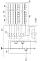
- the display device 100 in which the touch detection function is integrated functionally includes, for example, a control unit 601, a source driver 210, a gate driver 209, a COM power generation unit 602, and a Tx power source.
- a generation unit 603, a common line driving circuit 211, a sensor signal detection circuit 204, and the panel 200 are included.
- the control unit 601 controls each circuit. Specifically, for example, the control unit 601 controls each circuit by outputting a control signal for controlling each unit to the gate driver 209, the source driver 210, and the common line driving circuit 211. In addition, the control unit 601 receives a signal output from the sensor signal detection circuit, and performs processing such as calculation of touch coordinates and noise removal.
- control unit 601 may be composed of a single circuit or a plurality of circuits.
- a circuit for inputting a control signal to the gate driver 209 and the source driver 210 and a circuit for inputting a control signal to the sensor signal driving circuit may be provided separately.
- a circuit for processing a signal output from the sensor signal detection circuit may be provided separately.
- the control unit 601 is composed of a plurality of circuits, a circuit and wiring for synchronizing the circuits are required.
- the COM power generation unit 602 generates a COM potential.
- the COM potential is a potential that forms an electric field applied to the liquid crystal layer 406 arranged in each pixel together with the data signal when a data signal is applied to each pixel electrode 301.
- the Tx power generation unit 603 generates the Tx potential already described.
- the sensor signal detection circuit 204 detects a position where a finger or the like is in contact based on a signal acquired from the sensor signal detection line 202 of the panel 200 and a control signal of the control unit 601. I do.
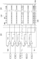
- the common line drive circuit 211 functionally includes a pulse generation unit 604 and a pulse compensation unit 605. Based on the control signal from the control unit 601, the pulse generation unit 604 generates a Tx signal that is a pulse signal for sequentially outputting to the plurality of common lines 208.
- the pulse compensation unit 605 is connected to the control unit 601, the pulse generation unit 604, the COM power generation unit 602, and the Tx power generation unit. Then, the pulse compensation unit 605 changes the potential of each source line 207 based on each Tx signal input from the pulse generation unit 604 and the potential input from all or part of each common line 208. Each common line drive signal that reduces the variation in potential of each common line 208 is generated. Then, the pulse compensation unit 605 outputs each common line drive signal to the corresponding common line 208.
- the pulse compensation unit 605 includes, for example, n operational amplifier circuits 701 corresponding to n common lines 208.
- Each operational amplifier circuit 701 includes one operational amplifier and two resistors. The two resistors included in each operational amplifier circuit 701 are connected in parallel to the negative terminal and output terminal of each operational amplifier, and the positive terminal of each operational amplifier is connected to the pulse generator 604, and the output terminal of each operational amplifier. Are connected to the common line 208 of the corresponding panel.
- each operational amplifier circuit 701 is an inverting amplifier circuit. Specifically, for example, signals from the corresponding Tx1 signal to the Txn signal are input from the pulse generation unit 604 to the positive terminal of each operational amplifier circuit 701. Further, the potential of the corresponding common line 208 is input to the negative terminal via a resistor. The output terminal of the operational amplifier outputs each common line drive signal obtained by adding each signal corresponding to the potential obtained by inverting the fluctuation of the potential of each common line 208 to each Tx signal to the corresponding common line 208. .
- the pulse compensation unit 605 includes an inverting amplifier circuit
- the pulse compensation unit 605 includes a configuration other than the inverting amplifier circuit as long as it has the same operation and effect.
- Other configurations may be used.
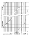
- FIG. 8 is a timing chart showing changes in potential with time of the G1 to Gm signals, the data signal, and the Tx1 to Txn signals.
- a period in which the G1 to Gm signals make one round is defined as one frame period.
- one frame period is divided into n, a period including a period in which the G1 signal is at a high potential is referred to as a first period, and each subsequent period is referred to as a second period to an nth period.
- each of the first to n-th periods corresponds to a period approximately four times as long as the high period input to one gate line 206.
- one common line 208 is arranged corresponding to each of the four gate lines 206.
- the gate driver 209 sequentially outputs pulses of G1 to G (m) signals to the m gate lines 206. Further, the source driver 210 outputs a data signal to each source line 207. Similarly, the Tx driver sequentially outputs pulses of Tx1 to Txn signals to n common lines.
- each Tx signal includes four pulses in each period (for example, the first period) of one frame period.
- signals G1 to Gm are gate signals output from the gate driver 209. Specifically, for example, pulses of the G1 to Gm signals are sequentially output to the m gate lines 206. Note that m and n may be different numbers, or the same number.
- the data signal is a signal output from the source driver 210.
- the number of data signals corresponds to the number of source lines 207 arranged on the panel, but in FIG. 8, for simplification of illustration, the number of data signals is omitted and only one is described. Yes.
- the Tx1 to Txn signals are pulse signals including a pulse in any period that does not overlap with each other from the first period to the nth period.
- the Tx1 signal is a pulse signal including four pulses in the nth period.
- the Tx2 to Txn signals are pulse signals including four pulses in the first period to the (n ⁇ 1) period, respectively.
- the Tx1 to Txn signals only need to include pulses only in one corresponding period among the first period to the nth period, and the order is not limited.
- FIG. 8 shows an example in which the Tx1 to Txn signals include four pulses in each period, but the number of times may be other than four.
- each pulse included in the Tx1 to Txn signals is included in a period different from a period in which each gate signal corresponding to each Tx signal includes a pulse.
- the Tx1 signal includes a pulse in the nth period. Therefore, the common line drive signal based on the Tx1 signal includes a pulse in the same nth period as the Tx1 signal, as described with reference to FIG.
- the Tx2 to Txn signals include pulses in a period different from a period in which each gate signal corresponding to each Tx signal includes a pulse.
- the common line 208 to which the common line drive signal is input is disposed corresponding to the gate line 206 to which the G1 to G4 signals are input, and the G1 to G4 signals include a pulse in the first period. Yes.
- FIG. 9 shows an example of the waveform shape of the common line drive signal input to the common line 208 in the period before and after the first period.
- Tx2 signal represents a signal generated by the pulse generation unit 604.
- Data signal represents a signal output from the source driver 210 to the source line 207.
- the “common line drive signal when there is no correction” represents the common line drive signal on the common line when not depending on the present embodiment.
- the “fluctuation of the potential of the common line due to the data signal” means that the data signal input to the source line 207 is given to the signal of the common line 208 through the parasitic capacitance formed between the source line 207 and the common line 208. Represents the variation in potential.
- the “inverted and amplified potential of the common line” represents a signal that is generated by the operational amplifier circuit 701 to which the fluctuation of the potential of the common line 208 is input and the fluctuation of the potential is inverted and amplified.
- the “common line drive signal output by the pulse compensator” represents the common line drive signal that has been output to the pulse compensator 605 and before being input to the common line 208 in the present embodiment.
- the “common line drive signal when there is correction” represents the common line drive signal on the common line 208 in the present embodiment.
- the “Tx2 signal” is converted into a common line drive signal via the pulse compensation unit 605 and input to the common line 208.
- the “fluctuation of the potential of the common line due to the data signal” is fed back to the inverting amplifier circuit. Then, the inverting amplifier circuit generates “inverted and amplified potential of the common line” representing a signal obtained by inverting the potential fluctuation based on “fluctuation of the potential of the common line due to the data signal”.
- the inverting amplifier circuit adds the input “Tx2 signal” and the waveform of the “inverted and amplified common line potential” to the common line having the waveform shown in “common line drive signal output by the pulse compensator”.
- a drive signal is output to the common line 208.
- the “inverted and amplified common line potential” included in the “common line drive signal output by the pulse compensator” input to the common line 208 is influenced by the “fluctuation of the potential of the common line due to the data signal”. Reduce. Specifically, as shown in FIG.
- the shape of the waveform of the common line drive signal on the common line 208 is the shape of the waveform indicated by the “common line drive signal when there is correction”, and is common when there is no correction. Compared with the line drive signal, it can be seen that the waveform shape of the common line drive signal at the timing immediately before the pulse is smoothed. Therefore, more effective touch detection is possible.
- the “common line drive signal when there is correction” has a potential variation caused by the “data signal” at the timing when each horizontal period starts, but the detection of touch is performed in a period in which the Tx signal includes a pulse. Therefore, the above effect can be obtained if the timing just before the pulse is flat.
- the data signal is illustrated as one of the causes of giving noise to the common line driving signal input to the common line 208, the data signal is not limited thereto.
- the pulse compensation unit 605 may be replaced with a configuration that achieves the same effect as the inverting amplifier circuit or a configuration that can achieve the same purpose.
- a second embodiment of the present invention will be described.
- the difference between the first embodiment and the second embodiment is that the pulse compensation unit 605 converts each signal obtained by inverting the fluctuation of the potential of each common line 208 into each Tx signal during the detection period in which touch detection is performed. This is a point to stop the adding operation.
- the second embodiment can reduce power consumption compared to the first embodiment.
- the other configurations of the second embodiment are the same as the configurations of the first embodiment, and therefore, duplicate description is omitted.
- FIG. 10 is a diagram illustrating an example of the panel 200 and the pulse compensation unit 605 of the display device 100 in which the touch detection function according to the second embodiment is integrated.
- FIG. 10 corresponds to FIG. 7 of the display device 100 in which the touch detection function according to the first embodiment is integrated.
- each operational amplifier circuit 701 included in the pulse compensation unit 605 one resistor and the negative of the operational amplifier are included.
- a circuit selection switch 1001 is provided between the side terminals. Since other points are the same as those in the first embodiment, description thereof is omitted.
- the control unit 601 switches the circuit selection switch 1001 so that the operational amplifier circuit 701 functions as an inverting amplifier circuit during a period when touch detection is not performed, and functions as a voltage follower during a period when touch detection is performed.
- the operational amplifier circuit 701 consumes less power than when functioning as an inverting amplifier circuit. Therefore, according to the present embodiment, it is possible to provide a display device integrated with a touch detection function that is thinner and has higher detection accuracy, and consumes the display device 100 with an integrated touch detection function. Electric power can be reduced.
- the operational amplifier circuit 701 functions as an inverting amplifier circuit as in the first embodiment when the circuit selection switch 1001 is in the ON state.
- the circuit selection switch 1001 when the circuit selection switch 1001 is in the off state, one of the two resistors is disconnected from the negative terminal of the operational amplifier, so that the operational amplifier circuit 701 consumes less power than the inverting amplifier circuit.
- the circuit selection switch 1001 is controlled to be turned on and off based on a control signal from the control unit 601.
- FIG. 11 is a timing chart showing an example of each timing of the G1 to Gm signals, the data signal, the Tx1 to Txn signals, and the SW1 to SWn. Note that a state in which the SW1 to SWn signals are at a high potential represents an on state of the circuit selection switch 1001, and a state in which the SW1 to SWn signals are at a low potential represents a low state of the circuit selection switch 1001. Further, the SW1 to n signals correspond to the circuit selection switch 1001 included in the operational amplifier circuit 701 to which the Tx1 to n signals are input, respectively.
- the SW1 to SWn signals are signals obtained by inverting the corresponding Tx1 to Txn signals, respectively. Therefore, the operational amplifier circuit 701 functions as a voltage follower that consumes less power than the inverting amplifier circuit when the Tx signal is at a high potential. Thus, the operational amplifier circuit 701 functions as an inverting amplifier circuit only during a period necessary for detection, and functions as a voltage follower during a period when the Tx signal necessary for detection is not output, thereby reducing power consumption.
- each TFT 302 that does not correspond represents a TFT 302 that does not apply a data signal to each pixel electrode, based on a common line 208 connected to an operational amplifier circuit 701 including a circuit selection switch 1001.
- the circuit selection switch 1001 may be switched on and off according to a timing chart as shown in FIG.
- the SW1 to SWn signals are high potentials in the first to nth periods in which the Tx signal corresponding to each SW signal includes a pulse. Is a signal.
- the SW1 to SWn signals are signals that become a high potential in a period in which a gate signal corresponding to each SW signal includes a pulse and a period subsequent to a period in which the gate signal includes a pulse.
- the SW1 signal has a low potential except for the n period in which the Tx1 signal corresponding to the SW1 signal includes a pulse, the first period in which the G1 to G4 signals include a pulse, and the second period. Signal.
- the SW1 signal may be at a low potential in the middle of the second period. According to this modification, the power consumption can be further reduced by increasing the period during which the operational amplifier circuit 701 functions as a voltage follower.
- timing charts shown in FIGS. 11 and 12 are examples, and the circuit selection switch 1001 may switch on and off based on other timing charts.
- the panel 200 includes a display area 1301 and a detection area 1302 that is different from the display area 1301.
- the pulse compensation unit 605 outputs each common line drive signal based on the potential input from the common line 208 arranged in the detection region 1302.
- the display region 1301 is a region where each pixel and each TFT 302 are arranged in each region partitioned by each source line 207 and each gate line 206.
- the detection region 1302 is a region different from the display region 1301 and is a region where each source line 207 and a part of the plurality of common lines 208 intersect each other.
- the other configuration of the third embodiment is the same as the configuration of the second embodiment, and a duplicate description is omitted.
- FIG. 13 is a diagram illustrating an example of the panel 200 and the pulse compensation unit 605 of the display device 100 in which the touch detection function according to the third embodiment is integrated.
- FIG. 13 corresponds to FIG. 10 of the display device 100 in which the touch detection function according to the second embodiment is integrated.
- a dedicated detection-dedicated electrode 1303 for detecting the fluctuation of the potential of the source electrode is arranged in the detection region 1302.
- each operational amplifier shares one of the two resistors included in each operational amplifier circuit 701.
- the shared resistor is connected to the negative terminal of the operational amplifier. Therefore, in the operational amplifier circuit 701 to which the shared resistor is connected, the potential of the dedicated common line 208 is fed back and input, and fluctuation in the potential of the common line drive signal to be output can be reduced.
- an operational amplifier circuit to which no shared resistor is connected functions as a voltage follower as described above.
- each operational amplifier circuit 701 shares a resistor. Therefore, compared to the second embodiment, one of the resistors arranged in each operational amplifier circuit 701 is unnecessary.
- the shared resistor is sequentially connected to each operational amplifier circuit 701 by a circuit selection switch 1001, and the operational amplifier circuit 701 operates as an inverting amplifier circuit during the connected period. Therefore, the shared resistor is the same as in the second embodiment.
- the waveform shape of the common line drive signal can be smoothed. Therefore, according to the third embodiment, it is possible to simplify the configuration of the pulse compensation unit 605 while having the same effect as compared with the second embodiment, and it is thinner and more detectable.
- a display device in which a highly accurate touch detection function is integrated can be provided.
- a fourth embodiment of the present invention will be described.
- the fourth embodiment is different from the third embodiment in that the pulse compensation unit 605 includes a signal selection unit 1401 and an output selection unit 1402.
- the signal selection unit 1401 and the output selection unit 1402 will be described later.
- the configuration of the pulse compensation unit 605 can be simplified as compared with the third embodiment.
- the other configuration of the fourth embodiment is the same as the configuration of the third embodiment, and thus redundant description is omitted.
- FIG. 14 is a diagram illustrating an example of the panel 200 and the pulse compensation unit 605 of the display device 100 in which the touch detection function according to the fourth embodiment is integrated, and the touch detection function according to the third embodiment is integrated. This corresponds to FIG. 13 of the converted display device 100.
- the pulse compensation unit 605 includes an operational amplifier circuit 701, a signal selection unit 1401, and an output selection unit 1402. Since the operational amplifier circuit 701 is the same as that of the first to third embodiments, the description thereof is omitted.
- the signal selection unit 1401 includes two resistors, two NchFETs (Field Effect Transistor), and one PchFET.
- the source terminal of one NchFET is grounded, the gate terminal is connected to the pulse generating unit 604, and the drain terminal is connected to the gate terminal of the other NchFET and one resistor.
- the source terminal of the other NchFET is connected to the output terminal of the operational amplifier in the operational amplifier circuit 701, and the drain terminal is connected to the source terminal of the PchFET and the output selection unit 1402.
- the gate terminal of the PchFET is connected to each of the two resistors, and the drain terminal is connected to one resistor and the Tx power supply generation unit 603.
- the output selection unit 1402 includes a switch whose output corresponds to each common line 208 arranged in the display area 1301 and whose input is connected to the signal selection unit 1401. Each of the switches is turned on and off by a control signal from the control unit 601.
- the signal selection unit 1401 selects the output of the operational amplifier circuit 701 while each Tx signal is in a high or low potential period. In the other period, the signal selection unit 1401 selects a signal corresponding to a potential different from the potential output from the operational amplifier circuit 701 in the one period, based on a high potential or a low potential power source.
- the signal selection unit 1401 turns off the NchFET to which the Tx signal is inputted and the PchFET, and turns on the NchFET connected to the operational amplifier circuit 701. Therefore, the signal selection unit 1401 outputs the signal input from the operational amplifier in the operational amplifier circuit 701 to the output selection unit 1402. Therefore, the signal output from the signal selection unit 1401 is added with the inversion component of the fluctuation of the potential of the common line 208 only during the low potential period.
- the output selection unit 1402 selects one common line 208 from the plurality of common lines 208 based on the timing of each Tx signal, and outputs the signal selected by the signal selection unit 1401 to the selected common line 208. Output. Specifically, for example, the switch included in the signal selection unit 1401 is in a period in which a touch on the corresponding common line 208 is detected and a period in which a voltage corresponding to the data signal is applied to the pixel corresponding to the common line 208. , The on state, and the off state in other periods. According to this embodiment, since the number of operational amplifiers in the operational amplifier circuit 701 is reduced, the circuit area can be reduced and the frame area can be reduced. In the fourth embodiment, the output selection unit 1402 may not be provided, and the signal selection unit 1401 corresponding to each common line 208 may be provided.
- a liquid crystal display device has been assumed.
- a display device using various light emitting elements such as an organic EL element, an inorganic EL element, and an FED (Field-Emission Device) may be used.
- the present invention is not limited to the above-described embodiment, and various modifications can be made.
- the configuration described in the embodiment can be replaced with substantially the same configuration, a configuration that exhibits the same operational effects, or a configuration that can achieve the same purpose.
Landscapes
- Engineering & Computer Science (AREA)
- Physics & Mathematics (AREA)
- Theoretical Computer Science (AREA)
- General Engineering & Computer Science (AREA)
- General Physics & Mathematics (AREA)
- Human Computer Interaction (AREA)
- Nonlinear Science (AREA)
- Chemical & Material Sciences (AREA)
- Crystallography & Structural Chemistry (AREA)
- Mathematical Physics (AREA)
- Optics & Photonics (AREA)
- Computer Hardware Design (AREA)
- Microelectronics & Electronic Packaging (AREA)
- Control Of Indicators Other Than Cathode Ray Tubes (AREA)
- Liquid Crystal Display Device Control (AREA)
Abstract
La présente invention porte sur un dispositif d'affichage mince doté d'une fonction de détection tactile intégrée ayant une précision de détection élevée. Ce dispositif d'affichage doté d'une fonction de détection tactile intégrée est caractérisé par le fait qu'il comprend : une pluralité de lignes de source et une pluralité de lignes de détection, qui s'étendent dans une première direction ; une pluralité de lignes communes et une pluralité de lignes de grille, qui s'étendent dans une seconde direction différente de la première direction ; une pluralité de pixels auxquels des signaux d'image correspondant à une image à afficher sont fournis par les lignes de source ; une pluralité de dispositifs de commande qui fournissent, aux pixels, des tensions qui sont basées sur les signaux d'image et les potentiels des lignes communes ; un circuit de pilotage de lignes communes qui comprend une unité de génération d'impulsion qui génère des premiers signaux d'impulsion pour piloter séquentiellement les lignes communes, et qui comprend en outre une unité de compensation d'impulsion qui, sur la base des premiers signaux d'impulsion et des potentiels reçus en provenance de tout ou partie des lignes communes, génère des deuxièmes signaux d'impulsion pour réduire des changements dans les potentiels des lignes communes en raison des potentiels des lignes de source et délivre chaque deuxième signal d'impulsion à l'une correspondante des lignes communes ; et une unité de détection tactile qui détecte une position pointée en réponse à chaque deuxième impulsion.
Priority Applications (2)
| Application Number | Priority Date | Filing Date | Title |
|---|---|---|---|
| PCT/JP2014/000931 WO2015125176A1 (fr) | 2014-02-21 | 2014-02-21 | Dispositif d'affichage doté d'une fonction de détection tactile intégrée |
| US15/243,267 US10007379B2 (en) | 2014-02-21 | 2016-08-22 | Display device with built-in touch detection function |
Applications Claiming Priority (1)
| Application Number | Priority Date | Filing Date | Title |
|---|---|---|---|
| PCT/JP2014/000931 WO2015125176A1 (fr) | 2014-02-21 | 2014-02-21 | Dispositif d'affichage doté d'une fonction de détection tactile intégrée |
Related Child Applications (1)
| Application Number | Title | Priority Date | Filing Date |
|---|---|---|---|
| US15/243,267 Continuation US10007379B2 (en) | 2014-02-21 | 2016-08-22 | Display device with built-in touch detection function |
Publications (1)
| Publication Number | Publication Date |
|---|---|
| WO2015125176A1 true WO2015125176A1 (fr) | 2015-08-27 |
Family
ID=53877722
Family Applications (1)
| Application Number | Title | Priority Date | Filing Date |
|---|---|---|---|
| PCT/JP2014/000931 Ceased WO2015125176A1 (fr) | 2014-02-21 | 2014-02-21 | Dispositif d'affichage doté d'une fonction de détection tactile intégrée |
Country Status (2)
| Country | Link |
|---|---|
| US (1) | US10007379B2 (fr) |
| WO (1) | WO2015125176A1 (fr) |
Families Citing this family (5)
| Publication number | Priority date | Publication date | Assignee | Title |
|---|---|---|---|---|
| KR102329050B1 (ko) * | 2015-04-17 | 2021-11-19 | 삼성디스플레이 주식회사 | 터치 패널 및 이의 제조방법 |
| JP6993168B2 (ja) * | 2017-10-18 | 2022-01-13 | 株式会社ジャパンディスプレイ | 表示装置、および、タッチパネル装置 |
| JP7112928B2 (ja) | 2018-09-28 | 2022-08-04 | 株式会社ジャパンディスプレイ | 表示装置 |
| CN115427922B (zh) * | 2020-06-15 | 2023-08-25 | 深圳市汇顶科技股份有限公司 | 打码方法、打码装置和触控芯片 |
| JP7623894B2 (ja) * | 2021-05-26 | 2025-01-29 | シャープ株式会社 | タッチパネル装置 |
Citations (5)
| Publication number | Priority date | Publication date | Assignee | Title |
|---|---|---|---|---|
| WO2006043660A1 (fr) * | 2004-10-22 | 2006-04-27 | Sharp Kabushiki Kaisha | Dispositif d’affichage avec capteur tactile et méthode de pilotage du dispositif |
| JP2011222013A (ja) * | 2010-04-06 | 2011-11-04 | Samsung Electronics Co Ltd | タッチパネルの寄生キャパシタンス補償方法及びその装置 |
| JP2012099081A (ja) * | 2010-11-04 | 2012-05-24 | Samsung Mobile Display Co Ltd | タッチスクリーンパネル一体型液晶表示装置 |
| JP2013084196A (ja) * | 2011-10-12 | 2013-05-09 | Lg Display Co Ltd | タッチパネルを備えた液晶表示装置およびその駆動方法 |
| JP2013109095A (ja) * | 2011-11-18 | 2013-06-06 | Lg Display Co Ltd | タッチパネルを備えた液晶表示装置およびその駆動方法 |
Family Cites Families (15)
| Publication number | Priority date | Publication date | Assignee | Title |
|---|---|---|---|---|
| DE3782858T2 (de) * | 1986-06-17 | 1993-04-08 | Fujitsu Ltd | Ansteuerung fuer eine anzeigevorrichtung in matrix-form. |
| JP4100383B2 (ja) * | 2003-10-31 | 2008-06-11 | セイコーエプソン株式会社 | 画像信号処理装置、画像信号処理方法、電気光学装置および電子機器 |
| JP2008304806A (ja) | 2007-06-11 | 2008-12-18 | Hitachi Displays Ltd | 液晶表示装置 |
| JP5203293B2 (ja) * | 2009-05-21 | 2013-06-05 | 株式会社ジャパンディスプレイウェスト | 表示装置および電子機器 |
| TWI431362B (zh) * | 2009-05-29 | 2014-03-21 | Japan Display West Inc | 觸控感測器、顯示器及電子裝置 |
| JP5191453B2 (ja) * | 2009-06-29 | 2013-05-08 | 株式会社ジャパンディスプレイウェスト | タッチセンサ、表示装置および電子機器 |
| US8411066B2 (en) * | 2010-01-05 | 2013-04-02 | 3M Innovative Properties Company | High speed noise tolerant multi-touch touch device and controller therefor |
| US9823785B2 (en) * | 2010-09-09 | 2017-11-21 | 3M Innovative Properties Company | Touch sensitive device with stylus support |
| GB201106350D0 (en) * | 2011-04-14 | 2011-06-01 | Plastic Logic Ltd | Display systems |
| US20130127794A1 (en) * | 2011-11-18 | 2013-05-23 | Qualcomm Mems Technologies, Inc. | Write waveform porch overlapping |
| JP2013246289A (ja) * | 2012-05-25 | 2013-12-09 | Panasonic Liquid Crystal Display Co Ltd | 液晶表示装置 |
| JP2013246737A (ja) * | 2012-05-28 | 2013-12-09 | Panasonic Liquid Crystal Display Co Ltd | エンベディッド型タッチスクリーン |
| JP5979988B2 (ja) * | 2012-05-31 | 2016-08-31 | 株式会社ジャパンディスプレイ | 液晶表示装置 |
| TWI471782B (zh) * | 2012-11-14 | 2015-02-01 | Orise Technology Co Ltd | 內嵌式多點觸控液晶顯示面板系統 |
| JP2014174851A (ja) * | 2013-03-11 | 2014-09-22 | Japan Display Inc | タッチセンサ装置、表示装置、及び電子機器 |
-
2014
- 2014-02-21 WO PCT/JP2014/000931 patent/WO2015125176A1/fr not_active Ceased
-
2016
- 2016-08-22 US US15/243,267 patent/US10007379B2/en active Active
Patent Citations (5)
| Publication number | Priority date | Publication date | Assignee | Title |
|---|---|---|---|---|
| WO2006043660A1 (fr) * | 2004-10-22 | 2006-04-27 | Sharp Kabushiki Kaisha | Dispositif d’affichage avec capteur tactile et méthode de pilotage du dispositif |
| JP2011222013A (ja) * | 2010-04-06 | 2011-11-04 | Samsung Electronics Co Ltd | タッチパネルの寄生キャパシタンス補償方法及びその装置 |
| JP2012099081A (ja) * | 2010-11-04 | 2012-05-24 | Samsung Mobile Display Co Ltd | タッチスクリーンパネル一体型液晶表示装置 |
| JP2013084196A (ja) * | 2011-10-12 | 2013-05-09 | Lg Display Co Ltd | タッチパネルを備えた液晶表示装置およびその駆動方法 |
| JP2013109095A (ja) * | 2011-11-18 | 2013-06-06 | Lg Display Co Ltd | タッチパネルを備えた液晶表示装置およびその駆動方法 |
Also Published As
| Publication number | Publication date |
|---|---|
| US20160357329A1 (en) | 2016-12-08 |
| US10007379B2 (en) | 2018-06-26 |
Similar Documents
| Publication | Publication Date | Title |
|---|---|---|
| US10572076B2 (en) | Touch display panel and associated driving circuit and driving method | |
| US9378699B2 (en) | Liquid crystal display device | |
| CN103941926B (zh) | 具有触控功能的显示装置 | |
| US9823788B2 (en) | Capacitive in-cell touch panel, display device, and driving method | |
| JP2017016560A (ja) | タッチ検出機能付き表示装置 | |
| KR20170070878A (ko) | 터치스크린 내장형 표시장치 및 구동방법 | |
| US10007379B2 (en) | Display device with built-in touch detection function | |
| US20170115798A1 (en) | Touch display panel and associated driving circuit and driving method | |
| EP3316237B1 (fr) | Écran d'affichage à commande tactile intégrée et procédé d'attaque associé ainsi que dispositif d'affichage | |
| US10481721B2 (en) | Display substrate having touch function, method for driving the same and display apparatus | |
| KR20140098022A (ko) | 표시 장치, 표시 장치의 구동 방법 및 전자 기기 | |
| TW201704965A (zh) | 觸控顯示面板 | |
| KR20110034188A (ko) | 액정 표시패널, 이를 포함하는 액정 표시장치 및 액정 표시장치의 구동 방법 | |
| CN102768423B (zh) | 显示装置 | |
| KR102098681B1 (ko) | 인 셀 터치 액정표시장치 | |
| US9524697B2 (en) | Capacitive touch screen display system including circuitry to address display perturbations induced by panel sensing | |
| US11269205B2 (en) | Display panel with charging control as well as liquid crystal display and control method associated therewith | |
| CN106708304B (zh) | 触控显示面板及相关的驱动电路及驱动方法 | |
| JP2016197400A (ja) | 表示装置 | |
| JP6263340B2 (ja) | 液晶表示装置 | |
| JP2014021799A (ja) | タッチパネル装置 | |
| JP2014167514A (ja) | 液晶表示装置及びその駆動方法 | |
| KR102260599B1 (ko) | 터치 디스플레이 장치의 구동 방법 | |
| JP2010210675A (ja) | 液晶表示装置 | |
| WO2012046633A1 (fr) | Dispositif d'affichage intégré d'entrée/sortie |
Legal Events
| Date | Code | Title | Description |
|---|---|---|---|
| 121 | Ep: the epo has been informed by wipo that ep was designated in this application |
Ref document number: 14883099 Country of ref document: EP Kind code of ref document: A1 |
|
| NENP | Non-entry into the national phase |
Ref country code: DE |
|
| 122 | Ep: pct application non-entry in european phase |
Ref document number: 14883099 Country of ref document: EP Kind code of ref document: A1 |
|
| NENP | Non-entry into the national phase |
Ref country code: JP |