WO2015125533A1 - Stratifié de film mince luminescent, procédé de production de stratifié de film mince luminescent, élément électroluminescent organique et procédé de fabrication d'élément électroluminescent organique - Google Patents
Stratifié de film mince luminescent, procédé de production de stratifié de film mince luminescent, élément électroluminescent organique et procédé de fabrication d'élément électroluminescent organique Download PDFInfo
- Publication number
- WO2015125533A1 WO2015125533A1 PCT/JP2015/051312 JP2015051312W WO2015125533A1 WO 2015125533 A1 WO2015125533 A1 WO 2015125533A1 JP 2015051312 W JP2015051312 W JP 2015051312W WO 2015125533 A1 WO2015125533 A1 WO 2015125533A1
- Authority
- WO
- WIPO (PCT)
- Prior art keywords
- layer
- thin film
- light emitting
- organic
- light
- Prior art date
- Legal status (The legal status is an assumption and is not a legal conclusion. Google has not performed a legal analysis and makes no representation as to the accuracy of the status listed.)
- Ceased
Links
Images


Classifications
-
- H—ELECTRICITY
- H10—SEMICONDUCTOR DEVICES; ELECTRIC SOLID-STATE DEVICES NOT OTHERWISE PROVIDED FOR
- H10K—ORGANIC ELECTRIC SOLID-STATE DEVICES
- H10K59/00—Integrated devices, or assemblies of multiple devices, comprising at least one organic light-emitting element covered by group H10K50/00
- H10K59/30—Devices specially adapted for multicolour light emission
- H10K59/32—Stacked devices having two or more layers, each emitting at different wavelengths
-
- H—ELECTRICITY
- H10—SEMICONDUCTOR DEVICES; ELECTRIC SOLID-STATE DEVICES NOT OTHERWISE PROVIDED FOR
- H10K—ORGANIC ELECTRIC SOLID-STATE DEVICES
- H10K50/00—Organic light-emitting devices
- H10K50/10—OLEDs or polymer light-emitting diodes [PLED]
- H10K50/11—OLEDs or polymer light-emitting diodes [PLED] characterised by the electroluminescent [EL] layers
- H10K50/125—OLEDs or polymer light-emitting diodes [PLED] characterised by the electroluminescent [EL] layers specially adapted for multicolour light emission, e.g. for emitting white light
- H10K50/13—OLEDs or polymer light-emitting diodes [PLED] characterised by the electroluminescent [EL] layers specially adapted for multicolour light emission, e.g. for emitting white light comprising stacked EL layers within one EL unit
- H10K50/131—OLEDs or polymer light-emitting diodes [PLED] characterised by the electroluminescent [EL] layers specially adapted for multicolour light emission, e.g. for emitting white light comprising stacked EL layers within one EL unit with spacer layers between the electroluminescent layers
Definitions
- the present invention relates to a light-emitting thin film laminate including one or more light-emitting organic semiconductor thin films, a method for producing the light-emitting thin film laminate, an organic electroluminescence device including the light-emitting thin film laminate, and an organic
- the present invention relates to a method for manufacturing an electroluminescence element.
- Examples of light-emitting electronic display devices include organic electroluminescence elements (organic EL elements).
- An organic EL device has a structure in which a light emitting layer containing a compound that emits light is sandwiched between a cathode and an anode, and injects electrons and holes into the light emitting layer to recombine excitons. It is an element that emits light by utilizing light emission (fluorescence / phosphorescence) when the exciton is deactivated. It can emit light at a voltage of several volts to several tens of volts, and is self-luminous, so it has a wide viewing angle and high visibility, and it is a thin-film, completely solid-state device that saves space and is portable. It attracts attention from the viewpoint of sex. Furthermore, the organic EL element has a feature that it is a surface light source.
- an organic EL element having a multi-unit structure has been reported by a multi-photon emission (MPE) technology in which light emitting units are connected in series by a charge generation layer and stacked in a plurality of stages (for example, patents). Reference 1).
- MPE multi-photon emission
- the organic EL element using the above-described MPE technology is provided with a plurality of light emitting layers for the purpose of extending the life of the element and increasing the luminance, and a charge generation layer is provided between the light emitting layer and the light emitting layer.
- the charge generation layer is configured, for example, by laminating an electron generation layer made of an inorganic semiconductor material having electron injection characteristics and a hole generation layer having hole injection characteristics. These electron generating layer and hole generating layer are formed by co-evaporation or vapor deposition alone.
- the organic EL element using the MPE technology has good performance, but the electron generation layer is formed by co-evaporation or vapor deposition alone, so that the production cost is low in terms of equipment investment, material utilization efficiency, and production speed. There is a problem of getting higher.
- a method for reducing the manufacturing cost a method of forming a charge generation layer by a wet method using an ionic polymer has been proposed (for example, see Patent Document 2).
- the performance of the entire device deteriorates due to the upper layer solvent penetrating into the lower organic film, dissolving the lower layer, roughing the lower surface, and promoting crystallization of the material constituting the lower layer.
- the laminated structure of the light emitting layer similar to the case where the vapor deposition method is used cannot be formed using the wet method. That is, it is not possible to realize a laminated structure of a light emitting layer or an organic EL element that can suppress functional degradation due to a solvent of a wet method.
- the present invention provides a light-emitting thin-film laminate and an organic electroluminescence device having a structure capable of suppressing functional degradation even when a wet method is used.
- the luminescent thin film laminate of the present invention includes at least one or more luminescent organic semiconductor thin films, an ALD thin film layer formed by an atomic layer deposition (ALD) method, and a wet layer above the ALD thin film layer. And at least one organic layer formed by the method. And the organic electroluminescent element of this invention is equipped with the said light emitting thin film laminated body.
- ALD atomic layer deposition
- the manufacturing method of the light emitting thin film laminated body of the present invention includes ALD using an atomic layer deposition (ALD) method after the step of forming the first organic layer and the step of forming the first organic layer.
- the method includes a step of forming a thin film layer and a step of forming a second organic layer using a wet method after the step of forming an ALD thin film layer.
- the manufacturing method of the organic electroluminescent element of this invention includes the manufacturing process of the said light emitting thin film laminated body.
- the atomic deposition (ALD) method is used to provide a dense and defect-free structure.
- ALD atomic deposition
- an organic layer is formed on the ALD thin film layer by a wet method.
- the dense and defect-free ALD thin film layer can suppress the penetration of the solvent used in the wet method into the lower layer.
- a wet method is used, a light-emitting thin film laminate and an organic electroluminescence element that can suppress lowering of the performance of the lower layer due to penetration of the solvent can be produced.
- Embodiment 2 of light-emitting thin film laminate 2.
- Manufacturing method of luminescent thin film laminate 3.
- Embodiment of organic electroluminescence device Method for manufacturing organic electroluminescence device
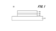
- Embodiment of Luminescent Thin Film Laminate> Specific embodiments of the luminescent thin film laminate of the present invention will be described below. In FIG. 1, the structure of the luminescent thin film laminated body of this embodiment is shown.
- the luminescent thin film laminate 10 shown in FIG. 1 includes a base material 11, a first luminescent layer 12, an intermediate layer 13, and a second luminescent layer 14. Specifically, in the luminescent thin film laminate 10, the first luminescent layer 12 is formed on the substrate 11. An intermediate layer 13 is formed on the first light emitting layer 12 by using an atomic layer deposition (ALD) method. Furthermore, a second light emitting layer 14 formed by a wet method is provided on the intermediate layer 13. The first light-emitting layer 12 and the second light-emitting layer 14 are configured to include at least one light-emitting organic semiconductor thin film (organic layer).
- ALD atomic layer deposition
- the base material 11 used for the light-emitting thin film laminate 10 is not particularly limited in the type of glass, plastic, and the like, and preferable examples include glass, quartz, and a transparent resin film. Particularly preferred is a resin film capable of imparting flexibility to the luminescent thin film laminate 10.
- polyesters such as polyethylene terephthalate (PET) and polyethylene naphthalate (PEN), polyethylene, polypropylene, cellophane, cellulose diacetate, cellulose triacetate (TAC), cellulose acetate butyrate, cellulose acetate propionate ( CAP), cellulose esters such as cellulose acetate phthalate, cellulose nitrate or derivatives thereof, polyvinylidene chloride, polyvinyl alcohol, polyethylene vinyl alcohol, syndiotactic polystyrene, polycarbonate, norbornene resin, polymethylpentene, polyether ketone, polyimide , Polyethersulfone (PES), polyphenylene sulfide, polysulfone , Polyetherimide, polyetherketoneimide, polyamide, fluororesin, nylon, polymethylmethacrylate, acrylic or polyarylates, cyclone resins such as Arton (trade name, manufactured by JSR) or Appel (trade name
- a barrier film made of an inorganic film, an organic film, or a hybrid film of both may be formed on the surface of the resin film.
- the barrier film had a water vapor transmission rate (25 ⁇ 0.5 ° C., relative humidity (90 ⁇ 2)% RH) of 0.01 g / (m 2 ⁇ 24 h) measured by a method according to JIS K 7129-1992.
- the following barrier films are preferred.
- the oxygen permeability measured by a method according to JIS K 7126-1987 is 10 ⁇ 3 ml / (m 2 ⁇ 24 h ⁇ atm) or less, and the water vapor permeability is 10 ⁇ 5 g / (m 2 ⁇ 24h)
- the following high-barrier film is preferable.
- the material for forming the barrier film may be any material that has a function of suppressing entry of elements such as moisture and oxygen.
- silicon oxide, silicon dioxide, silicon nitride, or the like can be used.
- the method for forming the barrier film is not particularly limited.
- the vacuum deposition method, sputtering method, reactive sputtering method, molecular beam epitaxy method, cluster ion beam method, ion plating method, plasma polymerization method, atmospheric pressure plasma weight A combination method, a plasma CVD method, a laser CVD method, a thermal CVD method, a coating method, or the like can be used.
- an atmospheric pressure plasma polymerization method as described in JP-A-2004-68143 is preferable.
- the first light emitting layer 12 is a layer including a light emitting organic semiconductor thin film that provides a field in which electrons and holes injected from an electrode or an adjacent layer are recombined to emit light via excitons.
- the first light emitting layer 12 preferably contains a light emitting dopant (a light emitting dopant compound, a dopant compound, also simply referred to as a dopant) and a host compound (a matrix material, a light emitting host compound, also simply referred to as a host).
- the formation method of the 1st light emitting layer 12 does not have a restriction
- the first light emitting layer 12 is preferably formed by a wet method from the manufacturing cost of the light emitting thin film laminate 10.
- Luminescent dopant As the luminescent dopant, a fluorescent luminescent dopant (also referred to as a fluorescent dopant or a fluorescent compound) and a phosphorescent dopant (also referred to as a phosphorescent dopant or a phosphorescent compound) are preferably used.
- the concentration of the light-emitting dopant in the light-emitting layer can be arbitrarily determined based on the specific dopant used and the device requirements.
- the concentration of the optical dopant may be contained at a uniform concentration relative to the thickness direction of the light emitting layer, or may have an arbitrary concentration distribution.
- the light emitting layer may contain a plurality of types of light emitting dopants. For example, a combination of dopants having different structures, or a combination of a fluorescent luminescent dopant and a phosphorescent luminescent dopant may be used. Thereby, arbitrary luminescent colors can be obtained.
- one or a plurality of light-emitting layers contain a plurality of light-emitting dopants having different emission colors and emit white light.
- the combination of light-emitting dopants that exhibit white but examples include a combination of blue and orange, a combination of blue, green, and red.
- the phosphorescent dopant is a compound in which light emission from an excited triplet is observed.
- the phosphorescent dopant is a compound that emits phosphorescence at room temperature (25 ° C.), and has a phosphorescence quantum yield of 0 at 25 ° C. .01 or more compounds.
- a preferable phosphorescence quantum yield is 0.1 or more.
- the phosphorescent quantum yield can be measured by the method described in Spectroscopic II, page 398 (1992 edition, Maruzen) of Experimental Chemistry Course 4 of the 4th edition.
- the phosphorescence quantum yield in a solution can be measured using various solvents.
- the phosphorescence emitting dopant used for the light emitting layer should just achieve the said phosphorescence quantum yield (0.01 or more) in any solvent.
- an excited state of the host compound is generated by recombination of carriers on the host compound to which carriers are transported. It is an energy transfer type in which light is emitted from the phosphorescent dopant by transferring this energy to the phosphorescent dopant.
- the other is a carrier trap type in which a phosphorescent dopant becomes a carrier trap, carrier recombination occurs on the phosphorescent dopant, and light emission from the phosphorescent dopant is obtained. In any case, it is a condition that the excited state energy of the phosphorescent dopant is lower than the excited state energy of the host compound.
- the phosphorescent dopant can be appropriately selected from known materials used for the light emitting layer of the organic EL element.
- specific examples of known phosphorescent dopants include compounds described in the following documents.
- Examples of the phosphorescent compound include compounds represented by general formula (4), general formula (5), and general formula (6) described in paragraphs [0185] to [0235] of JP2013-4245A, and Illustrative compounds (Pt-1 to Pt-3, Os-1, Ir-1 to Ir-45) can be preferably mentioned.
- Ir-46, Ir-47, and Ir-48 are shown below.
- a preferable phosphorescent dopant is an organometallic complex having Ir as a central metal. More preferably, a complex containing at least one coordination mode of a metal-carbon bond, a metal-nitrogen bond, a metal-oxygen bond, and a metal-sulfur bond is preferable.
- the fluorescent light-emitting dopant is a compound that can emit light from an excited singlet, and is not particularly limited as long as light emission from the excited singlet is observed.
- Examples of the fluorescent light-emitting dopant include anthracene derivatives, pyrene derivatives, chrysene derivatives, fluoranthene derivatives, perylene derivatives, fluorene derivatives, arylacetylene derivatives, styrylarylene derivatives, styrylamine derivatives, arylamine derivatives, boron complexes, coumarin derivatives, Examples include pyran derivatives, cyanine derivatives, croconium derivatives, squalium derivatives, oxobenzanthracene derivatives, fluorescein derivatives, rhodamine derivatives, pyrylium derivatives, perylene derivatives, polythiophene derivatives, rare earth complex compounds, and the like.
- a light emitting dopant using delayed fluorescence may be used as the fluorescent light emitting dopant.
- the luminescent dopant using delayed fluorescence include compounds described in, for example, International Publication No. 2011/156793, Japanese Patent Application Laid-Open No. 2011-213643, Japanese Patent Application Laid-Open No. 2010-93181, and the like.
- the host compound is a compound mainly responsible for charge injection and transport in the light emitting layer, and its own light emission is not substantially observed in the organic EL element.
- it is a compound having a phosphorescence quantum yield of phosphorescence of less than 0.1 at room temperature (25 ° C.), more preferably a compound having a phosphorescence quantum yield of less than 0.01.
- the mass ratio in the layer is 20% or more among the compounds contained in a light emitting layer.
- the excited state energy of a host compound is higher than the excited state energy of the light emission dopant contained in the same layer.
- a host compound may be used independently or may be used in combination of multiple types. By using a plurality of types of host compounds, it is possible to adjust the movement of electric charges, and it is possible to increase the efficiency of the organic EL element.
- the compound conventionally used with an organic EL element can be used.
- it may be a low molecular compound, a high molecular compound having a repeating unit, or a compound having a reactive group such as a vinyl group or an epoxy group.
- Tg glass transition temperature
- the glass transition point (Tg) is a value determined by a method based on JIS-K-7121 using DSC (Differential Scanning Colorimetry).
- the intermediate layer 13 includes an ALD thin film layer formed by the ALD method.
- the ALD method can control film formation of monomolecular and submolecular film thicknesses following the shape of a film formation target object as a base. For this reason, a very thin film of sub-nano order can be easily obtained with good reproducibility.
- a dense and defect-free thin film layer can be formed.
- a thin and defect-free layer By including the ALD thin film layer formed by the ALD method in the intermediate layer 13, a thin and defect-free layer can be formed.
- the penetration of the solvent into the first light emitting layer 12 can be suppressed. For this reason, dissolution of the first light emitting layer 12, surface roughness, crystallization of the material constituting the first light emitting layer 12, and the like due to the solvent can be suppressed, and deterioration in performance of the first light emitting layer 12 can be suppressed. Can do.
- the ALD method can be formed as a thin and defect-free layer, even when a light-emitting layer stack structure is formed using a wet method, the ALD thin film layer intervenes, so Damage to the organic layer can be suppressed. Accordingly, by interposing the ALD thin film layer as an intermediate layer 13 between the organic layers, a stacked structure of the organic layers can be realized using a wet method.
- the intermediate layer 13 can be a layer having a function of supplying electrons to the adjacent layer on the anode side and holes to the adjacent layer on the cathode side.
- a charge generation layer can be configured by a combination of a hole generation layer that generates holes and an electron generation layer that generates electrons.
- the intermediate layer 13 can be constituted by, for example, an intermediate electrode, an intermediate conductive layer, a charge generation layer, an electron extraction layer, a connection layer, or an intermediate insulating layer.
- the intermediate layer 13 may be formed of a plurality of layers.
- the manufacturing method of the other layers other than the ALD thin film layer is not particularly limited.
- the order of lamination of the layer formed by the ALD method and the layer formed by another manufacturing method is not particularly limited.
- the intermediate layer formed by a method other than the ALD method is formed by a wet method, it is preferably formed in an upper layer than the ALD thin film layer.
- the material used for the intermediate layer 13 is a known material that can be formed by ALD, for example, J. Appl. Phys. 97, 121301 (2005) [Surface chemistry of atomic layer deposition: A case study for Any material described in the trimethylaluminum / water process can be used without particular limitation.
- ITO indium tin oxide
- IZO indium zinc oxide
- Fullerenes such as C60, conductive organic layers such as oligothiophene, metal phthalocyanines, metal-free phthalocyanines, metal porphyrins, metal-free porphyrins Conductive organic compound layer such as class, and the like, but not limited thereto.
- an inorganic material In order to suppress the denseness of the ALD thin film layer, particularly the penetration of the solvent, it is preferable to use an inorganic material.
- the inorganic material it is preferable to use a metal, an inorganic oxide, or an inorganic nitride, and it is particularly preferable to use Zn, W, Zr, Y, or an oxide or nitride thereof. Further, it is preferable to use oxides of Zn, W, Zr and Y.
- the second light emitting layer 14 includes at least one light emitting organic semiconductor thin film formed by a wet method.
- the material of the second light emitting layer 14 is the same as that of the first light emitting layer 12 described above, and any material that can be applied to a wet method can be used without any particular limitation.
- Examples of the wet method include a spin coating method, a casting method, an ink jet method, a printing method, a die coating method, a blade coating method, a roll coating method, a spray coating method, a curtain coating method, and an LB method (Langmuir-Blodgett method).
- a method having high suitability for a roll-to-roll method such as a die coating method, a roll coating method, an ink jet method, or a spray coating method is preferable.
- a liquid medium for dissolving or dispersing the material of the organic layer for example, ketones such as methyl ethyl ketone and cyclohexanone, fatty acid esters such as ethyl acetate, halogenated hydrocarbons such as dichlorobenzene, toluene, xylene, Aromatic hydrocarbons such as mesitylene and cyclohexylbenzene, aliphatic hydrocarbons such as cyclohexane, decalin, and dodecane, and organic solvents such as DMF and DMSO can be used.
- the material of the organic layer can be dispersed by a dispersion method such as ultrasonic wave, high shearing force dispersion or media dispersion.
- another layer may be formed between the first light emitting layer and the intermediate layer. Further, another layer may be formed between the second light emitting layer and the intermediate layer.
- the layer is formed by a wet method above the intermediate layer, the effect of the ALD thin film layer that suppresses damage to the lower layer by the wet method can be obtained. For this reason, for example, even when there are other layers formed by a wet method or layers formed by a vapor deposition method between the first light emitting layer and the second light emitting layer and the intermediate layer, The layer can suppress penetration of the solvent. As described above, even when another layer is formed between the first light emitting layer or the second light emitting layer and the intermediate layer, the effect of the ALD thin film layer can be obtained.
- the structure in which the light emitting layer is formed as a single layer is described.
- other organic layers and inorganic layers for improving the function of the light emitting layer are formed above and below the light emitting layer. May be.
- the manufacturing method of these layers is not particularly limited, it is preferably formed by a wet method from the viewpoint of manufacturing cost.
- the structure provided with two light emitting layers is demonstrated, it is applicable also to the structure which has three or more light emitting layers.
- a light emitting thin film laminate can be produced.
- a light emitting thin film laminate in which all the light emitting layers are formed by a wet method can be produced.
- the first light emitting layer 12 is formed on the substrate 11.
- the method for producing the first light emitting layer 12 may be a wet method (wet process) or a vapor deposition method (dry process).
- the first light emitting layer 12 is preferably formed by a wet method from the manufacturing cost of the light emitting thin film laminate 10.
- Examples of the wet method include a spin coating method, a casting method, an ink jet method, a printing method, a die coating method, a blade coating method, a roll coating method, a spray coating method, a curtain coating method, and an LB method (Langmuir-Blodgett method).
- a method having high suitability for a roll-to-roll method such as a die coating method, a roll coating method, an ink jet method, or a spray coating method is preferable.
- a liquid medium for dissolving or dispersing the material of the organic layer for example, ketones such as methyl ethyl ketone and cyclohexanone, fatty acid esters such as ethyl acetate, halogenated hydrocarbons such as dichlorobenzene, toluene, xylene, Aromatic hydrocarbons such as mesitylene and cyclohexylbenzene, aliphatic hydrocarbons such as cyclohexane, decalin, and dodecane, and organic solvents such as DMF and DMSO can be used.
- the material of the organic layer can be dispersed by a dispersion method such as ultrasonic wave, high shearing force dispersion or media dispersion.
- the vapor deposition conditions vary depending on the type of compound used and the like, but generally a boat heating temperature of 50 ° C. to 450 ° C. and a vacuum degree of 10 ⁇ 6 Pa to 10 ⁇ 10 -2 Pa, deposition rate of 0.01 nm / sec ⁇ 50 nm / sec, a substrate temperature of -50 ° C. ⁇ 300 ° C., film thickness 0.1 nm ⁇ 5 [mu] m, preferably it is desirable to select appropriately the range of 5 nm ⁇ 200 nm.
- the intermediate layer 13 is formed on the first light emitting layer 12 by using the ALD method.
- the thickness of the intermediate layer 13 is preferably 1 to 100 nm, and more preferably 5 to 50 nm.
- the thickness of the intermediate layer 13 is 1 nm or more, not only a function as a charge generation layer but also an effect of the ALD thin film layer such as suppression of permeation of a solvent from fine defects can be appropriately obtained.
- the thickness is preferably 100 nm or less from the viewpoint of productivity.
- the layer formed by the ALD method is not particularly limited, and a material capable of forming the above-described intermediate layer 13 can be used.
- the intermediate layer 13 formed using the ALD method is preferably, for example, an inorganic substance, an inorganic oxide, an inorganic nitride, an inorganic sulfide, or an inorganic salt, and more preferably an inorganic substance or an inorganic oxide. It does not specifically limit as an inorganic substance, Metals, such as aluminum, silver, and gold
- the inorganic oxide is not particularly limited, and examples thereof include oxides such as zinc, aluminum, zirconium, yttrium, titanium, copper, tungsten, vanadium, and molybdenum, and composite oxides such as ITO and AZO.
- the inorganic oxide is at least one selected from ZnO, ZrO, Y 2 O 3 , WO 3 , TiO 2 , CuO, MoO 3 and V 2 O 5 from the viewpoint of physical properties such as work function and ionization potential. It is preferable to include.
- intermediate oxides such as ZnO x and ZrO x can be formed by adjusting the introduction time of each gas, the film formation temperature, and the pressure during film formation.
- the ALD method is a method of depositing atomic layers one by one by introducing two or more kinds of gases (first gas and second gas) alternately onto a film formation target. More specifically, first, a first gas (raw material gas) is introduced into the surface of a film formation target, for example, a base material (in this embodiment, the base material 11 on which the first light emitting layer 12 is formed). A first gas molecular layer (monoatomic layer) is formed. Next, the first gas is purged (removed) by introducing an inert gas (purge gas). Note that the gas molecule layer formed by the first gas is not purged even when an inert gas is introduced by chemical adsorption.
- a second gas for example, an oxidizing gas
- the formed first gas molecular layer is oxidized to form an inorganic film.
- the second gas is purged by introducing an inert gas, and one cycle of the ALD method is completed.
- the atomic layers are deposited one by one, and the intermediate layer 13 having a predetermined film thickness can be formed. Note that the ALD method can form a thin film including a shadow portion regardless of the unevenness of the surface of the film formation target.
- the surface of the film formation target needs to be activated in order to adsorb gas molecules to the film formation target.
- the film forming temperature is high to some extent.
- the film formation target is a resin material
- the film forming temperature is appropriately adjusted within a range not exceeding the glass transition temperature or the decomposition start temperature of the resin material.
- the temperature in the reactor is usually about 50 to 200 ° C.
- the deposition amount per cycle is usually 0.01 to 0.3 nm, and a desired film thickness is obtained by repeating the film forming cycle.
- the first gas is a gas obtained by vaporizing a single metal or metal compound
- the second gas can be an oxidizing gas
- the inert gas is a gas that does not react with the first gas or the second gas.
- the metal compound used for the first gas is not particularly limited as long as it contains a metal and can be vaporized.
- the metal compound include halides such as dichlorozinc, tetrachlorozirconium and hexachlorotungsten, and organometallic compounds such as trimethylaluminum, diethylzinc, copper acetylacetonate, zinc acetate, tungsten propoxide and vanadium isopropoxide.
- the source gas may be appropriately selected depending on the inorganic oxide film to be formed.
- the inorganic oxide of the intermediate layer 13 is zinc oxide, Zn, ZnCl 2 , ZnMe 2 , ZnEt 2, Zn (OAc) 2 and the like.
- middle layer 13 is a zirconium oxide
- the gas obtained by vaporizing a zirconium compound can be used as 1st gas.
- zirconium compounds include ZrCl 4 , ZrI 4 , Zr (OtBu) 4 , Zr (thd) 4 and the like.
- the gas obtained by vaporizing a titanium compound can be used as 1st gas.
- a titanium compound include titanium tetrachloride (TiCl 4) , titanium (IV) isopropoxide (Ti [(OCH) (CH 3 ) 2 ] 4 ), tetrakisdimethylaminotitanium ([(CH 3 ) 2 N ] 4 Ti, TDMATi), tetrakis (diethylamino) titanium (Ti [N (CH 2 CH 3) 2] 4, TDEATi) , and the like.
- the oxidizing gas used for the second gas is not particularly limited as long as it is a gas capable of oxidizing the gas molecular layer.
- oxygen (O 2 ) ozone (O 3 ), water (H 2 O), hydrogen peroxide (H 2 O 2 ), methanol (CH 3 OH), ethanol (C 2 H 5 OH) and the like are used. It is also possible to use oxygen radicals.
- a nitrogen radical can be used. Nitrogen radicals can be generated in the same manner as the oxygen radical generation described above.
- a rare gas helium, neon, argon, krypton, xenon
- nitrogen gas or the like can be used.
- Deposition system For forming the intermediate layer 13 by the ALD method, for example, a batch type ALD film forming apparatus or a roll-to-roll type film forming apparatus in which an ALD thin film layer is laminated on a film without transporting a substrate can be used.
- the introduction time of the first gas is preferably 0.05 to 10 seconds, more preferably 0.1 to 3 seconds, and 0.5 to 2 More preferably, it is seconds.
- the introduction time of the first gas is within the above range (0.05 seconds) or more, it is preferable because a sufficient time for forming the gas molecular layer can be secured.
- the introduction time of the first gas is within the above range (10 seconds or less), it is preferable because the time required for one cycle can be reduced.
- the introduction time of the inert gas for purging the first gas is preferably 0.05 to 10 seconds, more preferably 0.5 to 6 seconds, and 1 to 4 seconds. More preferably. It is preferable for the introduction time of the inert gas to be within the above range (0.05 seconds or more) because the first gas can be sufficiently purged. On the other hand, when the introduction time of the inert gas is within the above range (10 seconds or less), the time required for one cycle can be reduced, and the influence on the formed gas molecular layer is reduced.
- the introduction time of the second gas is preferably 0.05 to 10 seconds, and more preferably 0.1 to 3 seconds.
- the introduction time of the second gas is within the above range (0.05 seconds or more), it is preferable because sufficient time for oxidizing the gas molecular layer can be secured.
- the introduction time of the second gas is within the above range (10 seconds or less), it is preferable because the time required for one cycle can be reduced and side reactions are prevented.
- the introduction time of the inert gas for purging the second gas is preferably 0.05 to 10 seconds. It is preferable that the introduction time of the inert gas be within the above range (0.05 seconds) because the second gas can be sufficiently purged. On the other hand, when the introduction time of the inert gas is within the above range (10 seconds or less), it is preferable because the time required for one cycle can be reduced and the influence on the formed atomic layer is small.
- the intermediate layer 13 may be formed using a roll-to-roll film forming apparatus.
- the luminescent thin film laminate can be continuously produced by the roll-to-roll method. Therefore, if the intermediate layer 13 is formed using a roll-to-roll type film forming apparatus, the production is performed. This is preferable because of improved properties.
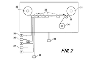
- a base material 32 on which a first light emitting layer and other layers are laminated as necessary is unwound from a feed roller 30 and wound by a take-up roller 31. Taken. Then, an intermediate layer is formed by the gas supplied from the coating head 33 while being conveyed from the feed roller 30 to the take-up roller 31.
- a protective film for protecting the base material 32 on which the ALD thin film layer is formed is supplied from the protective film roll 34 and conveyed to the take-up roller 31 together with the base material 32.
- an adhesive protective film it helps to protect the film surface on which the first light emitting layer is formed from damage, and is easy to install on an object to which the film on which the first light emitting layer is formed is applied.
- an adhesive protective film if it can apply to the film in which the 1st light emitting layer was formed, there will be no restriction
- an adhesive protective film formed of acrylic resin, urethane resin, epoxy resin, polyester resin, melamine resin, phenol resin, polyamide, ketone resin, vinyl resin, hydrocarbon resin, or the like can be used.
- the coating head 33 includes a raw material gas supply device 36 that supplies a first gas (raw material gas), an inert gas supply device 35 that supplies an inert gas, and A second gas supply device 37 for supplying a second gas and an exhaust pipe 38 are connected. Further, an exhaust pipe 39 for exhausting the entire roll-to-roll film forming apparatus is connected to the film forming apparatus.
- a raw material gas supply device 36 that supplies a first gas (raw material gas)
- an inert gas supply device 35 that supplies an inert gas
- a second gas supply device 37 for supplying a second gas and an exhaust pipe 38 are connected.
- an exhaust pipe 39 for exhausting the entire roll-to-roll film forming apparatus is connected to the film forming apparatus.
- the base 42 on which the first light emitting layer and other layers are laminated as necessary is unwound from the feed roller 41. Then, the base material 42 is supplied onto the main roll 44 through the guide roll 43. A coating head 45 is disposed on the main roll 44, and the substrate 42 is exposed to the gas supplied from the coating head 45. In the roll-to-roll apparatus, the temperature of the substrate 42 is appropriately adjusted by the temperature adjusting device 48 before being supplied to the coating head 45.
- the substrate 42 on which the ALD thin film layer is formed is wound up by a winding roller 47 through a guide roll 46.
- the guide roll 46 may be a stepped roll as disclosed in JP-A-2009-256709 so that the film blocking surface (ALD thin film layer) does not contact and the solvent blocking function does not deteriorate.
- the protective film for protecting the base material 42 in which the ALD thin film layer was formed is a protective film. Supplied from the roll 49 and conveyed to the take-up roller 47 together with the base material 42.
- the coating head 45 is supplied with a raw material gas supply device 50 for supplying a first gas (raw material gas), an inert gas supply device 54 for supplying an inert gas, and a second material.
- a second gas supply device 51 for supplying the gas and an exhaust pipe 52 are connected.
- an exhaust pipe 55 for exhausting the entire roll-to-roll film forming apparatus is connected to the film forming apparatus.
- FIG. 4 is a schematic diagram showing an example of a coating head for ALD film formation used in the apparatus shown in FIGS.
- the coating head 60 shown in FIG. 4 includes a source gas supply device 61 that supplies a first gas (source gas), an inert gas supply device 62 that supplies an inert gas, and a second gas that supplies a second gas. It has a supply device 63, a gas introduction pipe 64 and an exhaust pipe 65.
- the base material 66 on which the first light-emitting layer and other layers as necessary are stacked is conveyed in the A to B direction.
- the first gas (source gas) is supplied from the source gas supply device 61 to the base material 66 through the gas introduction pipe 64.
- the supplied gas is exhausted through the exhaust pipe 65.
- an inert gas is introduced into the substrate 66 from the inert gas supply device 62, and the source gas is purged (removed).
- a second gas (for example, oxidizing gas) is introduced from the second gas supply device 63 through the gas introduction pipe 64 to form an ALD thin film layer.
- the second gas is purged, and one cycle of the ALD method is completed.
- the inert gas and the second gas are exhausted through the exhaust pipe 65 before supplying the gas in the next process.
- the source gas and the second gas may be mixed with an inert gas (carrier gas) and supplied (see FIGS. 2 and 3).
- carrier gas inert gas
- the second light emitting layer 14 is formed on the intermediate layer 13.
- the second light emitting layer 14 is formed by a wet method.
- the wet method can be performed in the same manner as the wet method manufacturing method described in the description of the first light emitting layer 12 described above.
- the second light-emitting layer is formed by a wet method after the intermediate layer is formed by the ALD method.
- the solvent used for forming the second light emitting layer can be blocked by the intermediate layer, damage to the first light emitting layer due to the solvent can be suppressed.
- the influence of the solvent is not exerted on the lower layer. For this reason, a luminescent thin film laminated body can be manufactured using a wet method.
- another layer can be formed between the first light emitting layer and the intermediate layer, and between the second light emitting layer and the intermediate layer.
- Other layers can also be made.
- other layers for improving the function of the light emitting layer can be formed above and below the light emitting layer, and three or more light emitting layers can be formed.
- a layer is formed by a wet method on an upper layer than the intermediate layer, an effect of the ALD thin film layer that suppresses damage to the lower layer by a solvent used in the wet method can be obtained.
- the organic EL element 20 includes a base material 21, an anode 22, a first light emitting unit 23, an intermediate layer 24, a second light emitting unit 25, and a cathode 26.
- the anode 22 is formed on the base material 21.
- a first light emitting unit 23 and a second light emitting unit 25 are stacked on the anode 22 via an intermediate layer 24.
- a cathode 26 is provided on the second light emitting unit 25, and the first light emitting unit 23, the intermediate layer 24, and the second light emitting unit 25 are sandwiched between the cathode 26 facing the anode 22.
- the configuration in which the first light emitting unit 23 and the second light emitting unit 25 are laminated via the intermediate layer 24 is the same as that of the above-described embodiment of the light emitting thin film laminate. be able to.
- the organic EL element 20 is a structure provided with the above-mentioned luminescent thin film laminated body as a light emitting element.
- middle layer 24, the 2nd light emission unit 25, and the cathode 26 is demonstrated.
- middle layer 24 can be set as the structure similar to the base material and intermediate
- the first light emitting unit 23 and the second light emitting unit 25 have at least one light emitting layer.
- the light emitting layer included in the first light emitting unit 23 can have the same configuration as the first light emitting layer of the above-described embodiment of the light emitting thin film laminate.
- the light emitting layer contained in the 2nd light emitting unit 25 can be set as the structure similar to the 2nd light emitting layer of embodiment of the above-mentioned light emitting thin film laminated body. For this reason, detailed description is abbreviate
- FIG. 1 is abbreviate
- an electrode material made of a metal, an alloy, an electrically conductive compound, and a mixture thereof having a high work function (4 eV or more, preferably 4.3 V or more) is used.
- an electrode substance include metals such as Au and Ag, alloys thereof, and conductive transparent materials such as CuI, indium tin oxide (ITO), SnO 2 , and ZnO.
- amorphous material such as IDIXO (In 2 O 3 —ZnO) capable of forming a transparent conductive film may be used.
- a thin film may be formed by depositing these electrode materials by a method such as vapor deposition or sputtering, and a pattern having a desired shape may be formed by a photolithography method.
- a pattern may be formed through a mask having a desired shape during vapor deposition or sputtering of the electrode material.
- wet film-forming methods such as a printing system and a coating system, can also be used.
- the transmittance be larger than 10%.
- the sheet resistance as the anode is several hundred ⁇ / sq. The following is preferred. Further, although the thickness of the anode depends on the material, it is usually selected in the range of 10 nm to 1 ⁇ m, preferably 10 nm to 200 nm.
- the first light emitting unit 23 is provided between the anode 22 and the intermediate layer 24 and includes at least one light emitting layer including an organic material layer having light emitting properties. Further, the first light emitting unit 23 may include another layer between the light emitting layer and the anode 22 or the intermediate layer 24.
- Typical element configurations of the first light emitting unit 23 include the following configurations, but are not limited thereto.
- the configuration of (7) is preferably used, but is not limited thereto.
- the light emitting layer is formed of a single layer or a plurality of layers.
- a hole blocking layer (hole blocking layer), an electron injection layer (cathode buffer layer), or the like may be provided between the light emitting layer and the cathode, and between the light emitting layer and the anode.
- An electron blocking layer (electron barrier layer), a hole injection layer (anode buffer layer), or the like may be provided.
- the electron transport layer is a layer having a function of transporting electrons.
- the electron transport layer includes an electron injection layer and a hole blocking layer in a broad sense. Further, the electron transport layer may be composed of a plurality of layers.
- the hole transport layer is a layer having a function of transporting holes.
- the hole transport layer includes a hole injection layer and an electron blocking layer in a broad sense.
- the hole transport layer may be composed of a plurality of layers.
- the electron transport layer used for the organic EL element 20 is made of a material having a function of transporting electrons and has a function of transmitting electrons injected from the cathode to the light emitting layer.
- the electron transport material may be used alone or in combination of two or more.
- the total thickness of the electron transport layer is not particularly limited, but is usually in the range of 2 nm to 5 ⁇ m, more preferably 2 nm to 500 nm, and further preferably 5 nm to 200 nm.
- the organic EL element 20 when light generated in the light emitting layer is extracted, light extracted directly from the light emitting layer through the anode 22 and light extracted after being reflected by the cathode 26 positioned opposite to the anode 22 are extracted. , Known to cause interference. Therefore, in the organic EL element 20, it is preferable to adjust the total thickness of the first light emitting unit 23 by appropriately adjusting the total thickness of the electron transport layer between several nm to several ⁇ m. On the other hand, since the voltage when the thickness of the electron transport layer tends to increase, especially in the case a thick film thickness, the electron mobility of the electron transport layer is preferably 10 -5 cm 2 / Vs or more .
- the material used for the electron transport layer may have any of the electron injection property or the transport property or the hole barrier property. Any one can be selected and used. Examples thereof include nitrogen-containing aromatic heterocyclic derivatives, aromatic hydrocarbon ring derivatives, dibenzofuran derivatives, dibenzothiophene derivatives, silole derivatives, and the like.
- nitrogen-containing aromatic heterocyclic derivatives examples include carbazole derivatives, azacarbazole derivatives (one or more carbon atoms constituting the carbazole ring are substituted with nitrogen atoms), pyridine derivatives, pyrimidine derivatives, pyrazine derivatives, pyridazine derivatives, triazine derivatives.
- aromatic hydrocarbon ring derivative examples include naphthalene derivatives, anthracene derivatives, triphenylene and the like.
- a metal complex having a quinolinol skeleton or a dibenzoquinolinol skeleton as a ligand such as tris (8-quinolinol) aluminum (Alq3), tris (5,7-dichloro-8-quinolinol) aluminum, tris (5,7- Dibromo-8-quinolinol) aluminum, tris (2-methyl-8-quinolinol) aluminum, tris (5-methyl-8-quinolinol) aluminum, bis (8-quinolinol) zinc (Znq), etc., and metal complexes thereof
- a metal complex in which the central metal is replaced with In, Mg, Cu, Ca, Sn, Ga, or Pb can also be used as an electron transporting material.
- metal-free or metal phthalocyanine, or those having the terminal substituted with an alkyl group or a sulfonic acid group can be preferably used as the electron transporting material.
- the distyrylpyrazine derivative exemplified as the material for the light emitting layer can also be used as an electron transport material, and an inorganic semiconductor such as n-type-Si, n-type-SiC, etc. as in the case of the hole injection layer and the hole transport layer. Can also be used as an electron transporting material.
- a polymer material in which these materials are introduced into a polymer chain or these materials are used as a polymer main chain can also be used.
- the electron transport layer may be doped with a doping material as a guest material to form an electron transport layer having a high n property (electron rich).
- the doping material include metal compounds such as metal complexes and metal halides, and other n-type dopants.
- Specific examples of the electron transport layer having such a structure include, for example, JP-A-4-297076, JP-A-10-270172, JP-A-2000-196140, 2001-102175, J. Appl. Phys., 95, 5773 (2004) and the like.
- preferable electron transport materials include, but are not limited to, compounds described in the following documents.
- U.S. Pat.No. 6,528,187, U.S. Pat.No. 7,230,107 U.S. Patent Publication No. 20050025993, U.S. Pat. Publication No. 2004036077, U.S. Pat. Publication No. 200901115316, U.S. Pat. 2003060956, WO200008132085, Appl. Phys. Lett. 75, 4 (1999), Appl. Phys. Lett. 79, 449 (2001), Appl. Phys. Lett. 81, 162 (2002), Appl. Phys. Lett. 81, 162 (2002), Appl. Phys. Lett. 81, 162 (2002), Appl. Phys.
- More preferable electron transport materials include pyridine derivatives, pyrimidine derivatives, pyrazine derivatives, triazine derivatives, dibenzofuran derivatives, dibenzothiophene derivatives, carbazole derivatives, azacarbazole derivatives, and benzimidazole derivatives.
- the hole blocking layer is a layer having a function of an electron transport layer in a broad sense. Preferably, it is made of a material having a function of transporting electrons and a small ability to transport holes. By blocking holes while transporting electrons, the recombination probability of electrons and holes can be improved. Moreover, the structure of the above-mentioned electron carrying layer can be used as a hole-blocking layer as needed.
- the hole blocking layer provided in the organic EL element 20 is preferably provided adjacent to the cathode side of the light emitting layer.
- the thickness of the hole blocking layer is preferably in the range of 3 to 100 nm, more preferably in the range of 5 to 30 nm.
- the material used for the hole blocking layer the material used for the above-described electron transport layer is preferably used, and the material used as the above-described host compound is also preferably used for the hole blocking layer.
- the electron injection layer (also referred to as “cathode buffer layer”) is a layer provided between the cathode and the light emitting layer in order to lower the driving voltage and improve the light emission luminance.
- An example of an electron injection layer can be found in the second chapter, Chapter 2, “Electrode Materials” (pages 123-166) of “Organic EL devices and their industrialization front line (issued by NTT Corporation on November 30, 1998)”. Are listed.
- the electron injection layer is provided as necessary, and is provided between the cathode and the light emitting layer or between the cathode and the electron transport layer as described above.
- the electron injection layer is preferably a very thin film, and the film thickness is preferably in the range of 0.1 nm to 5 nm, depending on the material.
- membrane in which a constituent material exists intermittently may be sufficient.
- JP-A-6-325871, JP-A-9-17574, and JP-A-10-74586 Specific examples of materials preferably used for the electron injection layer include metals typified by strontium and aluminum, alkali metal compounds typified by lithium fluoride, sodium fluoride, and potassium fluoride, magnesium fluoride, and fluoride. Examples thereof include alkaline earth metal compounds typified by calcium, metal oxides typified by aluminum oxide, metal complexes typified by lithium 8-hydroxyquinolate (Liq), and the like.
- the material used for said electron injection layer may be used independently, and may be used in combination of multiple types.
- the hole transport layer is made of a material having a function of transporting holes.
- the hole transport layer is a layer having a function of transmitting holes injected from the anode to the light emitting layer.
- the total thickness of the hole transport layer is not particularly limited, but is usually in the range of 5 nm to 5 ⁇ m, more preferably 2 nm to 500 nm, and further preferably 5 nm to 200 nm.
- the material used for the hole transport layer may have any of a hole injection property or a transport property and an electron barrier property.
- a hole transport material an arbitrary material can be selected and used from conventionally known compounds.
- the hole transport material may be used alone or in combination of two or more.
- Hole transport materials include, for example, porphyrin derivatives, phthalocyanine derivatives, oxazole derivatives, oxadiazole derivatives, triazole derivatives, imidazole derivatives, pyrazoline derivatives, pyrazolone derivatives, phenylenediamine derivatives, hydrazone derivatives, stilbene derivatives, polyarylalkane derivatives, tria Reelamine derivatives, carbazole derivatives, indolocarbazole derivatives, isoindole derivatives, acene derivatives such as anthracene and naphthalene, fluorene derivatives, fluorenone derivatives, polyvinyl carbazole, polymer materials having aromatic amine introduced in the main chain or side chain, or Oligomer, polysilane, conductive polymer or oligomer (eg, PEDOT: PSS, aniline copolymer, polyaniline, polythiophene, etc.) And the like.
- PEDOT PEDOT: PS
- triarylamine derivatives examples include a benzidine type typified by ⁇ -NPD, a starburst type typified by MTDATA, and a compound having fluorene or anthracene in the triarylamine linking core part.
- hexaazatriphenylene derivatives described in JP-T-2003-519432 and JP-A-2006-135145 can also be used as the hole transport material.
- a hole transport layer having a high p property doped with impurities can also be used.
- the configurations described in JP-A-4-297076, JP-A-2000-196140, 2001-102175, J. Appl. Phys., 95, 5773 (2004), etc. can also be applied to the transport layer.
- so-called p-type hole transport materials and p-type materials as described in JP-A-11-251067 and J. Huang et.al. (Applied Physics Letters 80 (2002), p. 139).
- Inorganic compounds such as -Si and p-type -SiC can also be used.
- ortho-metalated organometallic complexes having Ir or Pt as the central metal as typified by Ir (ppy) 3 are also preferably used.
- the hole transport material the above materials can be used, but a triarylamine derivative, a carbazole derivative, an indolocarbazole derivative, an azatriphenylene derivative, an organometallic complex, or an aromatic amine is introduced into the main chain or side chain.
- the polymer materials or oligomers used are preferably used.
- Specific examples of the hole transport material include, but are not limited to, the compounds described in the following documents in addition to the documents listed above. Appl. Phys. Lett. 69, 2160 (1996), J. Lumin. 72-74, 985 (1997), Appl. Phys. Lett. 78, 673 (2001), Appl. Phys. Lett. 90, 183503 (2007) ), Appl. Phys.
- the electron blocking layer is a layer having a function of a hole transport layer in a broad sense. Preferably, it is made of a material having a function of transporting holes and a small ability to transport electrons.
- the electron blocking layer can improve the probability of recombination of electrons and holes by blocking electrons while transporting holes.
- the structure of the above-mentioned hole transport layer can be used as an electron blocking layer of the organic EL element 20 as needed.
- the electron blocking layer provided in the organic EL element 20 is preferably provided adjacent to the anode side of the light emitting layer.
- the thickness of the electron blocking layer is preferably in the range of 3 to 100 nm, and more preferably in the range of 5 to 30 nm.
- the materials used for the electron blocking layer can be preferably used.
- the material used as the above-mentioned host compound can also be preferably used as the electron blocking layer.
- the hole injection layer (also referred to as “anode buffer layer”) is a layer provided between the anode and the light emitting layer in order to lower the driving voltage and improve the light emission luminance.
- An example of the hole injection layer is “Organic EL device and its industrialization front line (November 30, 1998, issued by NTT)”, Chapter 2, Chapter 2, “Electrode material” (pages 123-166). It is described in.
- the hole injection layer is provided as necessary, and is provided between the anode and the light emitting layer or between the anode and the hole transport layer as described above.
- Examples of the material used for the hole injection layer include the materials used for the hole transport layer described above. Among them, phthalocyanine derivatives typified by copper phthalocyanine, hexaazatriphenylene derivatives as described in JP-T-2003-519432 and JP-A 2006-135145, metal oxides typified by vanadium oxide, amorphous carbon, polyaniline ( Preferred are conductive polymers such as emeraldine) and polythiophene, orthometalated complexes represented by tris (2-phenylpyridine) iridium complex, and triarylamine derivatives.
- the materials used for the hole injection layer described above may be used alone or in combination of two or more.
- the first light emitting unit 23 constituting the organic EL element 20 may further contain other inclusions.
- the inclusion include halogen elements such as bromine, iodine, and chlorine, halogenated compounds, alkali metals such as Pd, Ca, and Na, alkaline earth metals, transition metal compounds, complexes, and salts.
- the content of the inclusion can be arbitrarily determined, but is preferably 1000 ppm or less, more preferably 500 ppm or less, and even more preferably 50 ppm or less with respect to the total mass% of the contained layer. . However, it is not within this range depending on the purpose of improving the transportability of electrons and holes or the purpose of favoring the exciton energy transfer.
- the second light emitting unit 25 at least one layer is formed by a wet method.
- the light emitting layer is formed by a wet method.
- the organic layer is preferably formed by a wet method. Furthermore, it is preferable that all the organic layers are formed by a wet method.
- the configuration of the second light emitting unit 25 can be the same as the configuration of the first light emitting unit 23 described above except that it has a layer formed by a wet method. For this reason, if it is a structure applicable to a wet method, the structure similar to the above-mentioned 1st light emission unit 23 can be used without specifically limiting.
- an electrode substance made of a metal (referred to as an electron injecting metal) having a small work function (4 eV or less), an alloy, an electrically conductive compound, and a mixture thereof is used.
- electrode materials include sodium, sodium-potassium alloy, magnesium, lithium, magnesium / copper mixture, magnesium / silver mixture, magnesium / aluminum mixture, magnesium / indium mixture, aluminum / aluminum oxide (Al 2 O 3 ) Mixtures, indium, lithium / aluminum mixtures, aluminum, silver, silver-based alloys, aluminum / silver mixtures, rare earth metals, and the like.
- the cathode 26 can be produced by using the above electrode material by a method such as vapor deposition or sputtering.
- the sheet resistance of the cathode 26 is several hundred ⁇ / sq. The following is preferred.
- the thickness of the cathode 26 is usually selected in the range of 10 nm to 5 ⁇ m, preferably 50 nm to 200 nm.
- the anode 22 is formed on the base material 21.
- the anode 22 is formed into a pattern having a desired shape by a photolithography method by forming a thin film by a method such as vapor deposition or sputtering using the electrode material used for the anode 22 described above.
- the pattern may be formed through a mask having a desired shape when the electrode material is formed by vapor deposition or sputtering.
- a wet film forming method such as a printing method or a coating method can also be used.
- a first light emitting unit 23 (a hole injection layer, a hole transport layer, a light emitting layer, a hole blocking layer, an electron transport layer, an electron injection layer, or the like) is formed on the anode 22.
- the formation method of the 1st light emission unit 23 does not have a restriction
- Examples of the wet method include a spin coating method, a casting method, an ink jet method, a printing method, a die coating method, a blade coating method, a roll coating method, a spray coating method, a curtain coating method, and an LB method (Langmuir-Blodgett method).
- a method having high suitability for a roll-to-roll method such as a die coating method, a roll coating method, an ink jet method, or a spray coating method is preferable.
- examples of the liquid medium for dissolving or dispersing the material of the first light emitting unit 23 include ketones such as methyl ethyl ketone and cyclohexanone, fatty acid esters such as ethyl acetate, halogenated hydrocarbons such as dichlorobenzene, toluene, and the like.
- Aromatic hydrocarbons such as xylene, mesitylene and cyclohexylbenzene, aliphatic hydrocarbons such as cyclohexane, decalin and dodecane, and organic solvents such as DMF and DMSO can be used.
- it can disperse
- the vapor deposition conditions vary depending on the type of compound used, etc., but generally a boat heating temperature of 50 ° C. to 450 ° C. and a degree of vacuum of 10 ⁇ 6 Pa— It is desirable to select appropriately within the range of 10 ⁇ 2 Pa, vapor deposition rate of 0.01 nm / second to 50 nm / second, substrate temperature of ⁇ 50 ° C. to 300 ° C., film thickness of 0.1 nm to 5 ⁇ m, preferably 5 nm to 200 nm.
- the intermediate layer 24 is formed on the first light emitting unit 23 by using the ALD method.
- an ALD thin film layer can be formed using the same method as the intermediate layer described in the embodiment of the light emitting thin film laminate.
- the layer formed by the ALD method is not particularly limited, and a material capable of forming the intermediate layer described in the above embodiment of the light-emitting thin film stack can be used.
- the second light emitting unit 25 is formed on the intermediate layer 24.
- the 2nd light emission unit 25 forms at least 1 layer or more by a wet method.
- the wet method can be performed in the same manner as the wet method manufacturing method described in the description of the first light emitting unit 23 described above.
- the cathode 26 is formed on the second light emitting unit 25.
- the cathode 26 can be manufactured by using a method such as vapor deposition or sputtering of the electrode material used for the cathode 26 described above.
- the sheet resistance of the cathode 26 is several hundred ⁇ / sq. The following is preferred.
- the thickness of the cathode is usually selected in the range of 10 nm to 5 ⁇ m, preferably 50 nm to 200 nm.
- a wet film forming method such as a printing method or a coating method can be used.
- the produced organic EL element 20 is sealed.
- the sealing means used for sealing the organic EL element include a method in which a sealing member, an electrode, and a supporting base material are bonded with an adhesive.
- a sealing member it should just be arrange
- transparency and electrical insulation are not particularly limited.
- the sealing member In order to process the sealing member into a concave shape, sandblasting, chemical etching, or the like is used. In order to reduce the thickness of the organic EL element, it is preferable to use a polymer film or a metal film.
- the polymer film has an oxygen permeability measured by a method according to JIS K 7126-1987 of 1 ⁇ 10 ⁇ 3 ml / (m 2 / 24h) or less, and was measured by a method according to JIS K 7129-1992.
- water vapor permeability 25 ⁇ 0.5 ° C., relative humidity (90 ⁇ 2)%) is preferably at 1 ⁇ 10 -3 g / (m 2 / 24h) or less.
- the adhesive examples include photocuring and thermosetting adhesives having reactive vinyl groups such as acrylic acid oligomers and methacrylic acid oligomers, and moisture curing adhesives such as 2-cyanoacrylates. be able to.
- hot-melt type polyamide, polyester, and polyolefin can be mentioned.
- a cationic curing type ultraviolet curing epoxy resin adhesive can be mentioned.
- the sealing film it is preferable to have a laminated structure of an inorganic layer and a layer made of an organic material, like the above-described barrier film.
- the method for forming these films is not particularly limited. For example, vacuum deposition method, sputtering method, reactive sputtering method, molecular beam epitaxy method, cluster ion beam method, ion plating method, plasma polymerization method, atmospheric pressure plasma A polymerization method, a plasma CVD method, a laser CVD method, a thermal CVD method, a coating method, or the like can be used.
- the organic EL element of the embodiment described above is a surface light emitter, it can be used as various light emission sources.
- lighting devices such as home lighting and interior lighting, backlights for clocks and liquid crystals, lighting for billboard advertisements, light sources for traffic lights, light sources for optical storage media, light sources for electrophotographic copying machines, light sources for optical communication processors, Examples include, but are not limited to, a light source of an optical sensor, and can be effectively used as a backlight of a liquid crystal display device combined with a color filter and a light source for illumination.
- the organic EL element may be used as a kind of lamp for illumination or an exposure light source, a projection device that projects an image, or a display device that directly recognizes a still image or a moving image ( It may be used as a display.
- the light emitting surface may be enlarged by so-called tiling, in which light emitting panels provided with organic EL elements are joined together in a plane.
- the drive method when used as a display device for moving image reproduction may be either a simple matrix (passive matrix) method or an active matrix method.
- a color or full-color display device can be manufactured by using two or more organic EL elements having different emission colors.
- the organic EL element used for the lighting device may be designed such that the organic EL element having the configuration of the above-described embodiment has a resonator structure.
- Examples of the purpose of use of the organic EL element configured as a resonator structure include, but are not limited to, a light source of an optical storage medium, a light source of an electrophotographic copying machine, a light source of an optical communication processor, a light source of an optical sensor, and the like. .
- the material used for the organic EL element can be applied to an organic EL element that emits substantially white light (also referred to as a white organic EL element).
- a plurality of light emitting materials can simultaneously emit a plurality of light emission colors to obtain white light emission by color mixing.
- three emission maximum wavelengths of three primary colors of red, green, and blue may be included, or two emission using a complementary color relationship such as blue and yellow, blue green and orange, etc.
- a maximum wavelength may be included.
- a combination of light emitting materials for obtaining a plurality of emission colors includes a combination of a plurality of phosphorescent or fluorescent materials, a light emitting material that emits fluorescent or phosphorescent light, and light from the light emitting material as excitation light.
- a combination with a dye material that emits light may also be used.
- a plurality of light emitting dopants may be combined and mixed.
- Such a white organic EL element is different from a configuration in which organic EL elements emitting each color are individually arranged in parallel to obtain white light emission, and the organic EL element itself emits white light. For this reason, a mask is not required for the formation of most layers constituting the element, and for example, a conductive layer can be formed on one surface by vapor deposition, casting, spin coating, ink jet, printing, etc., and productivity is improved. .
- a light emitting material used for the light emitting layer of such a white organic EL element For example, if it is a backlight in a liquid crystal display element, it will adapt to the wavelength range corresponding to CF (color filter) characteristic.
- any material may be selected and combined from the metal complexes described in the embodiment of the organic EL element described above or a known light-emitting material and whitened.
- the lighting device can increase the area of the light emitting surface by using, for example, a plurality of organic EL elements.
- the light emitting surface is enlarged by arranging a plurality of light emitting panels provided with organic EL elements on the base material (that is, tiling) on the supporting base material.
- the supporting base material may also serve as a sealing material, and each light emitting panel is tiled in a state where the organic EL element is sandwiched between the supporting base material and the base material of the light emitting panel.
- An adhesive may be filled between the support substrate and the substrate, thereby sealing the organic EL element.
- the anode and cathode terminals are exposed around the light emitting panel.
- the center of each light emitting panel is a light emitting region, and a non-light emitting region is generated between the light emitting panels.
- a light extraction member for increasing the amount of light extracted from the non-light-emitting area may be provided in the non-light-emitting area of the light extraction surface.
- a light collecting sheet or a light diffusion sheet can be used as the light extraction member.
- Each of the light-emitting thin film stacks of Samples 101 to 107 was fabricated so that the area of the light emitting region was 5 cm ⁇ 5 cm. In the following, the configuration of each of the light-emitting thin film stacks of Samples 101 to 107 and the manufacturing procedure are shown.
- an atmospheric pressure plasma discharge treatment having a configuration described in Japanese Patent Application Laid-Open No. 2004-68143 is formed on the entire surface of a polyethylene naphthalate film (a film made by Teijin-Dyupon Co., Ltd., hereinafter abbreviated as PEN) on the side where the first electrode layer is formed.
- a polyethylene naphthalate film a film made by Teijin-Dyupon Co., Ltd., hereinafter abbreviated as PEN
- an inorganic gas barrier film made of SiOx is formed to a thickness of 500 nm, and a gas barrier having an oxygen permeability of 0.001 ml / m 2 / day or less and a water vapor permeability of 0.001 g / m 2 / day or less.
- Flexible films were prepared.
- a 120 nm-thick ITO (indium tin oxide) film was formed on the gas barrier flexible film by a sputtering method and patterned by a photolithography method to form a first electrode layer. In addition, it was set as the pattern so that a light emission area might be 50 mm x 50 mm.
- the first light emitting layer was formed to a thickness of 40 nm on the base material formed up to the first electrode layer using a wet method.
- the first light-emitting layer was prepared by preparing the following light-emitting layer composition, and then coating the substrate on which the first electrode layer was formed at a rate of 5 m / min by a die coating method, followed by natural drying, and then at 120 ° C. for 30 minutes. Retained and formed.
- a ZnO intermediate layer having a thickness of 5 nm was formed on the first light-emitting layer by ALD.
- the intermediate layer was formed using the ALD film forming apparatus having the configuration shown in FIG. 2 described in the embodiment of the organic EL element.
- a substrate formed up to the first light emitting layer was attached to the ALD film forming apparatus, a coating head for 150 cycles was prepared, and evacuation was performed to 100 Pa or less. Thereafter, each gas was allowed to flow through the coating head under the following film forming conditions to form an intermediate layer of ZnO, and then a protective film was attached and wound up.
- Film-forming conditions Film-forming material N 2 + ZnEt 2 (0.062 mol / L): 100 sccm Oxidizing gas N 2 + H 2 O (0.01 mol / L): 100 sccm Purge gas N 2 : 1000 sccm Substrate transport speed: 10 m / min Substrate temperature: 100 ° C
- a second light emitting layer was formed to a thickness of 40 nm on the intermediate layer by a wet method.
- the second light emitting layer was formed by the same method as the first light emitting layer described above.
- the sealing base material was adhere
- a laminated aluminum foil manufactured by Toyo Aluminum Co., Ltd.
- PET polyethylene terephthalate
- a two-component reactive urethane adhesive layer for dry lamination having a thickness of 1.5 ⁇ m was used.
- thermosetting adhesive as a sealing adhesive was uniformly applied to the aluminum surface of the sealing substrate with a thickness of 20 ⁇ m along the adhesive surface (glossy surface) of the aluminum foil using a dispenser. This was dried under a vacuum of 100 Pa or less for 12 hours. Furthermore, it moved to a nitrogen atmosphere with a dew point temperature of ⁇ 80 ° C. or lower and an oxygen concentration of 0.8 ppm, dried for 12 hours or longer, and adjusted the water content of the sealing adhesive to 100 ppm or lower.
- thermosetting adhesive an epoxy adhesive mixed with the following (A) to (C) was used.
- DGEBA Bisphenol A diglycidyl ether
- DIY Dicyandiamide
- C Epoxy adduct curing accelerator
- the sample in which the sealing base material was placed in close contact was tightly sealed using a pressure roll under pressure bonding conditions of a pressure roll temperature of 120 ° C., a pressure of 0.5 MPa, and an apparatus speed of 0.3 m / min.
- a luminescent thin film laminate of Sample 101 having the same form as the luminescent thin film laminate having the configuration shown in FIG. 1 was manufactured.
- a light-emitting thin film laminate of Sample 102 was produced in the same manner as Sample 101 described above, except that ZnO was formed by vapor deposition as the intermediate layer. (Intermediate layer-evaporation)
- the base material formed to the 1st light emitting layer was fixed to the base material holder of a commercially available vacuum evaporation apparatus, and was attached to the vacuum chamber of the vacuum evaporation apparatus. Further, ZnO was put into a resistance heating boat made of tungsten and attached in the vacuum chamber.
- the resistance heating boat was energized and heated, and the intermediate layer made of ZnO was deposited at 4 nm with a deposition rate of 0.1 nm / sec to 0.2 nm / sec. Formed in thickness.
- a light-emitting thin film laminate of Sample 103 was produced in the same manner as Sample 101 described above, except that an ALD precursor was applied as an intermediate layer and then oxidized to form ZnO. did.
- the coating solution was prepared in a nitrogen gas atmosphere, and all solvents were dehydrated and degassed before use. Diethyl ether (0.54 g) was added to diisopropyl ether (200 g), and the mixture was sufficiently stirred and filtered to obtain a coating solution. Next, the prepared coating solution was applied at a rate of 5 m / min by a die coating method and naturally dried, and then kept at 100 ° C. for 30 minutes to obtain an intermediate layer of 5 nm of ZnO.
- a light-emitting thin film laminate of Sample 104 was produced in the same manner as Sample 101 described above, except that the intermediate layer was formed by applying a polymer as described below and then curing the polymer.
- a chlorobenzene solution of DBp-6 and AIp-4 (each ratio is 50.0% by mass: 50.0% by mass) is formed on the first light-emitting layer by a die coating method.
- a low-pressure mercury lamp (15 mW / The polymer groups of DBp-6 and AIp-4 were photocured by UV irradiation at 130 ° C. for 30 seconds using cm 2 ) to provide an insolubilized n-type intermediate layer (CGL) having a thickness of 20 nm.
- n-type intermediate layer a chlorobenzene solution of DCp-3 and DCp-2 (each ratio is 85.0% by mass: 15.0% by mass) is formed by a die coating method. Thereafter, the polymerized groups of DCp-3 and DCp-2 were photocured by UV irradiation at 130 ° C. for 30 seconds using a low-pressure mercury lamp (15 mW / cm 2 ), and an insolubilized p-type intermediate layer having a thickness of 20 nm. (CGL) was provided. In the die coating method used at this time, the base material was fed at a speed of 5 m / min for coating.
- the light-emitting thin film laminate of Sample 105 was formed in the same manner as Sample 101 described above except that the intermediate layer was formed by forming a coating film containing ZnO particles as follows and then curing the coating film. Produced.
- Intermediate layer-ZnO particles A 2-propanol dispersion of ZnO nanoparticles (average particle size 20 nm) manufactured by Cai Kasei Co., Ltd. was applied at a rate of 5 m / min by a die coating method, naturally dried, and then kept at 100 ° C. for 30 minutes, and an intermediate layer of 20 nm ZnO Got.
- a luminescent thin film laminate of Sample 106 was manufactured in the same manner as Sample 101 described above, except that the intermediate layer was not manufactured. Therefore, the light-emitting thin film laminate of the sample 106 has a configuration in which the first light-emitting layer and the second light-emitting layer are directly laminated without having an intermediate layer.
- the sample 101 in which the intermediate layer is formed using the ALD method has higher emission intensity than the other samples, and is improved to 190 compared to the single layer.
- a value close to twice that of a single-layer phosphor is obtained, and the effect of laminating two light-emitting layers is sufficiently obtained.
- the samples 102 to 106 in which the intermediate layer is formed by a method other than the ALD method can only obtain a light emission amount that is about 1.5 times that of a single-layer light emitter, and the effect of stacking two light emitting layers is sufficient. It is not obtained.
- PEN polyethylene naphthalate film
- an atmospheric pressure plasma discharge treatment apparatus having a configuration described in Japanese Patent Application Laid-Open No. 2004-68143 is used to form an inorganic substance made of SiOx so as to have a thickness of 500 nm.
- a gas barrier layer was continuously formed.
- ITO indium tin oxide
- the base material formed up to the hole injection layer is transferred to a nitrogen atmosphere using nitrogen gas (grade G1), and a hole transport layer composition having the following composition is used to form a die coating method at 5 m / min. After coating and air drying, the film was kept at 130 ° C. for 30 minutes to provide a hole transport layer having a layer thickness of 30 nm.
- the base material formed up to the hole transport layer was coated at a rate of 5 m / min by a die coating method using a light emitting layer composition having the following composition, naturally dried, and then held at 120 ° C. for 30 minutes to obtain a layer thickness.
- a 50 nm light emitting layer was provided.
- Luminescent layer composition Host compound S-5: 11.79 parts by mass Phosphorescent dopant D-67: 0.05 parts by mass Isopropyl acetate: 2000 parts by mass
- n-type intermediate layer (hole generating layer) made of ZnO is formed on the first light emitting unit by using the ALD method, and a p-type intermediate layer (electron generating layer) is formed on the n-type intermediate layer. Laminated and formed.
- a ZnO intermediate layer having a thickness of 5 nm was formed by the ALD method in the same manner as the intermediate layer of the light-emitting thin film laminate of Sample 101 described above.
- a p-type intermediate layer was formed by a 10 nm WO 3 thin film on the ZnO intermediate layer.
- the WO 3 thin film was prepared by applying a mixed solution of tungsten isopropoxide and 2-propanol mixed at 1: 1 at a rate of 5 m / min by a die coating method, followed by air drying, and then transferring to the atmosphere at 100 ° C. for 60 ° C. Formed by holding for a minute.
- a second light emitting unit having a layer configuration excluding the hole injection layer was produced on the intermediate layer using the same method as that for the first light emitting unit described above.
- the organic EL element formed by the above steps is covered with a sealing material made of a glass substrate having a thickness of 300 ⁇ m, and the adhesive (sealing material) is interposed between the transparent sealing material and the substrate in a state of surrounding the organic EL element. ).
- a sealing material made of a glass substrate having a thickness of 300 ⁇ m
- the adhesive is interposed between the transparent sealing material and the substrate in a state of surrounding the organic EL element.
- an epoxy photocurable adhesive (Luxtrac LC0629B manufactured by Toagosei Co., Ltd.) was used.
- the adhesive was irradiated with UV light from the glass substrate (transparent sealing material) side, the adhesive was cured, and the organic EL element was sealed.
- an organic EL element of Sample 202 was fabricated in the same manner as Sample 201 described above, except that ZnO was formed by vapor deposition.
- the base material formed up to the first light emitting unit was fixed to a base material holder of a commercially available vacuum vapor deposition apparatus and attached to a vacuum chamber of the vacuum vapor deposition apparatus. Further, ZnO was put into a resistance heating boat made of tungsten and attached in the vacuum chamber. Next, after reducing the vacuum chamber to 4 ⁇ 10 ⁇ 4 Pa, the resistance heating boat is energized and heated, and the n-type intermediate layer made of ZnO is deposited at a deposition rate of 0.1 nm / second to 0.2 nm / second. Was formed with a thickness of 4 nm.
- an organic EL device of sample 203 was prepared in the same manner as sample 201 described above, except that an ALD precursor was applied and then the precursor was oxidized to form ZnO.
- the n-type intermediate layer was formed by the same method as the intermediate layer of the light-emitting thin film laminate of Sample 103 described above.
- Electrode transport layer On the light emitting layer, a 1,1,1-3,3,3-hexafluoroisopropanol solution of OC-107 was formed by a slit coating method. After film formation, a low pressure mercury lamp (15 mW / cm 2 ) was used. By UV irradiation at 130 ° C. for 30 seconds, the following polymer group of OC-107 was photocured to provide an insolubilized electron transport layer having a thickness of 20 nm.
- Luminous efficiency and lifetime were measured for each of the organic EL elements of Samples 201 to 205 produced as described above. Luminous efficiency is measured at room temperature (25 ° C) at a constant current density of 2.5 mA / cm 2 and each element is measured using a spectral radiance meter CS-2000 (manufactured by Konica Minolta Optics). The light emission luminance was measured, and the light emission efficiency (external extraction efficiency) at the current value was determined. The light emission luminance of each element was obtained from a relative value when the light emission efficiency of the single layer organic EL element of the sample 205 was set to 100.
- the lifetime was measured by continuously driving the organic EL element, measuring the luminance using the spectral radiance meter CS-2000, and determining the time (half-life) when the measured luminance was halved as a measure of the lifetime.
- the driving condition was set to a current value of 4000 cd / m 2 at the start of continuous driving.
- the lifetime of each element was calculated
- FIG. The results are shown in Table 2 below.
- the sample 201 in which the intermediate layer is formed by using the ALD method has higher luminous efficiency and lifetime than the other samples, and the luminous efficiency is improved to about 190 compared with the single layer.
- This is an organic EL element in which two light-emitting layers are stacked, and a value close to twice that of a single-layer organic EL element is obtained, and the effect of stacking two light-emitting layers is sufficiently obtained.
- the lifetime is improved by about 1.4 times as much as other samples, and the effect of improving the luminous efficiency and the influence on the first light emitting unit by the coating solvent when forming the second light emitting unit. The effect of reducing is sufficiently obtained.
- the samples 202 to 204 in which the intermediate layer is formed by a method other than the ALD method have a maximum lifetime of up to 150, but have a maximum lifetime of only about 1.1 times that of a single-layer organic EL element. Absent. Therefore, the effect of stacking two light emitting layers as an organic EL element is not sufficiently obtained.
- the upper layer and lower layer notations used for explaining the configuration of the light-emitting thin film laminate and the organic electroluminescence element are the layer configuration and the stacking order based on the base material. Is shown. That is, in the structure laminated
Landscapes
- Physics & Mathematics (AREA)
- Optics & Photonics (AREA)
- Electroluminescent Light Sources (AREA)
Abstract
La présente invention concerne un stratifié de film mince luminescent conçu pour comprendre : une couche de film mince ALD qui est formée par un procédé de dépôt de couche atomique et qui comprend au moins un film mince semi-conducteur luminescent organique ; et au moins une couche organique qui est formée au-dessus de la couche de film mince ALD par un procédé humide.
Priority Applications (1)
| Application Number | Priority Date | Filing Date | Title |
|---|---|---|---|
| JP2016504003A JPWO2015125533A1 (ja) | 2014-02-21 | 2015-01-20 | 発光性薄膜積層体、発光性薄膜積層体の製造方法、有機エレクトロルミネッセンス素子、及び、有機エレクトロルミネッセンス素子の製造方法 |
Applications Claiming Priority (2)
| Application Number | Priority Date | Filing Date | Title |
|---|---|---|---|
| JP2014031442 | 2014-02-21 | ||
| JP2014-031442 | 2014-02-21 |
Publications (1)
| Publication Number | Publication Date |
|---|---|
| WO2015125533A1 true WO2015125533A1 (fr) | 2015-08-27 |
Family
ID=53878049
Family Applications (1)
| Application Number | Title | Priority Date | Filing Date |
|---|---|---|---|
| PCT/JP2015/051312 Ceased WO2015125533A1 (fr) | 2014-02-21 | 2015-01-20 | Stratifié de film mince luminescent, procédé de production de stratifié de film mince luminescent, élément électroluminescent organique et procédé de fabrication d'élément électroluminescent organique |
Country Status (2)
| Country | Link |
|---|---|
| JP (1) | JPWO2015125533A1 (fr) |
| WO (1) | WO2015125533A1 (fr) |
Cited By (2)
| Publication number | Priority date | Publication date | Assignee | Title |
|---|---|---|---|---|
| JP2017509132A (ja) * | 2014-03-14 | 2017-03-30 | ネーデルランドセ・オルガニサティ・フォール・トゥーヘパスト−ナトゥールウェテンスハッペライク・オンデルズーク・テーエヌオー | 積層有機発光ダイオードの製造方法、積層oledデバイス、及びそれを製造するための装置 |
| CN111628095A (zh) * | 2020-06-08 | 2020-09-04 | 京东方科技集团股份有限公司 | Oled显示基板及其制作方法、显示面板、显示装置 |
Citations (4)
| Publication number | Priority date | Publication date | Assignee | Title |
|---|---|---|---|---|
| JP2012014905A (ja) * | 2010-06-30 | 2012-01-19 | Konica Minolta Holdings Inc | 有機エレクトロルミネッセンス素子、照明装置、表示装置及び有機エレクトロルミネッセンス素子の製造方法 |
| JP2012507123A (ja) * | 2008-10-30 | 2012-03-22 | オスラム オプト セミコンダクターズ ゲゼルシャフト ミット ベシュレンクテル ハフツング | 有機発光素子および有機発光素子の製造方法 |
| JP2012510706A (ja) * | 2008-12-01 | 2012-05-10 | イー・アイ・デュポン・ドウ・ヌムール・アンド・カンパニー | 有機電子デバイス用のアノード |
| EP2722413A1 (fr) * | 2012-10-18 | 2014-04-23 | Nederlandse Organisatie voor toegepast -natuurwetenschappelijk onderzoek TNO | Procédé de fabrication d'un élément semi-conducteur multicouche et élément semi-conducteur fabriqué en tant que tel |
-
2015
- 2015-01-20 WO PCT/JP2015/051312 patent/WO2015125533A1/fr not_active Ceased
- 2015-01-20 JP JP2016504003A patent/JPWO2015125533A1/ja active Pending
Patent Citations (4)
| Publication number | Priority date | Publication date | Assignee | Title |
|---|---|---|---|---|
| JP2012507123A (ja) * | 2008-10-30 | 2012-03-22 | オスラム オプト セミコンダクターズ ゲゼルシャフト ミット ベシュレンクテル ハフツング | 有機発光素子および有機発光素子の製造方法 |
| JP2012510706A (ja) * | 2008-12-01 | 2012-05-10 | イー・アイ・デュポン・ドウ・ヌムール・アンド・カンパニー | 有機電子デバイス用のアノード |
| JP2012014905A (ja) * | 2010-06-30 | 2012-01-19 | Konica Minolta Holdings Inc | 有機エレクトロルミネッセンス素子、照明装置、表示装置及び有機エレクトロルミネッセンス素子の製造方法 |
| EP2722413A1 (fr) * | 2012-10-18 | 2014-04-23 | Nederlandse Organisatie voor toegepast -natuurwetenschappelijk onderzoek TNO | Procédé de fabrication d'un élément semi-conducteur multicouche et élément semi-conducteur fabriqué en tant que tel |
Cited By (2)
| Publication number | Priority date | Publication date | Assignee | Title |
|---|---|---|---|---|
| JP2017509132A (ja) * | 2014-03-14 | 2017-03-30 | ネーデルランドセ・オルガニサティ・フォール・トゥーヘパスト−ナトゥールウェテンスハッペライク・オンデルズーク・テーエヌオー | 積層有機発光ダイオードの製造方法、積層oledデバイス、及びそれを製造するための装置 |
| CN111628095A (zh) * | 2020-06-08 | 2020-09-04 | 京东方科技集团股份有限公司 | Oled显示基板及其制作方法、显示面板、显示装置 |
Also Published As
| Publication number | Publication date |
|---|---|
| JPWO2015125533A1 (ja) | 2017-03-30 |
Similar Documents
| Publication | Publication Date | Title |
|---|---|---|
| CN104979482B (zh) | 有机电致发光元件及电子器件 | |
| WO2017195669A1 (fr) | Matériau d'élément électroluminescent organique, élément électroluminescent organique, appareil d'affichage et appareil d'éclairage | |
| JP6146415B2 (ja) | 有機エレクトロルミネッセンス素子、照明装置及び表示装置 | |
| JP6417821B2 (ja) | 有機エレクトロルミネッセンス素子及び照明装置 | |
| CN111244313A (zh) | 有机电致发光元件、有机电致发光元件的制造方法、显示装置及照明装置 | |
| CN107534092A (zh) | 有机电致发光元件用材料、有机电致发光元件、显示装置及照明装置 | |
| JP6939795B2 (ja) | 透明電極及び電子デバイス | |
| JP2016225498A (ja) | 有機エレクトロルミネッセンス素子 | |
| WO2015087795A1 (fr) | Élément électroluminescent organique, dispositif d'éclairage et dispositif d'affichage | |
| JP6592915B2 (ja) | 透明電極基板とその製造方法、電子デバイス及び有機elデバイス | |
| WO2015151684A1 (fr) | Élément électroluminescent organique et dispositif électronique | |
| JP6197404B2 (ja) | 有機エレクトロルミネッセンス素子、及び、電子機器 | |
| JP6941160B2 (ja) | 有機エレクトロルミネッセンス素子及び有機エレクトロルミネッセンス素子の製造方法 | |
| WO2015125533A1 (fr) | Stratifié de film mince luminescent, procédé de production de stratifié de film mince luminescent, élément électroluminescent organique et procédé de fabrication d'élément électroluminescent organique | |
| JP6996869B2 (ja) | 有機エレクトロルミネッセンス素子 | |
| JP2017079181A (ja) | 光変換材料、光変換フィルム、及び発光素子 | |
| JP5472107B2 (ja) | 有機エレクトロルミネセンス素子の製造方法 | |
| JPWO2014200067A1 (ja) | 有機エレクトロルミネッセンス素子、及び、電子機器 | |
| JP7351310B2 (ja) | 有機エレクトロルミネッセンス素子用の混合組成物 | |
| JP2018190608A (ja) | 有機エレクトロルミネッセンス素子 | |
| WO2017104242A1 (fr) | Matière d'élément électroluminescent organique, élément électroluminescent organique, dispositif d'affichage et dispositif d'éclairage | |
| WO2014109265A1 (fr) | Électrode transparente et dispositif électronique | |
| CN107278384B (zh) | 透明电极及电子器件 | |
| JPWO2019146396A1 (ja) | 発光性薄膜、発光性積層膜、有機エレクトロルミネッセンス素子、及びその製造方法 | |
| CN110431919A (zh) | 透明电极以及电子器件 |
Legal Events
| Date | Code | Title | Description |
|---|---|---|---|
| 121 | Ep: the epo has been informed by wipo that ep was designated in this application |
Ref document number: 15751457 Country of ref document: EP Kind code of ref document: A1 |
|
| ENP | Entry into the national phase |
Ref document number: 2016504003 Country of ref document: JP Kind code of ref document: A |
|
| NENP | Non-entry into the national phase |
Ref country code: DE |
|
| 122 | Ep: pct application non-entry in european phase |
Ref document number: 15751457 Country of ref document: EP Kind code of ref document: A1 |