WO2015137152A1 - Cellule solaire à hétérojonction et son procédé de production - Google Patents
Cellule solaire à hétérojonction et son procédé de production Download PDFInfo
- Publication number
- WO2015137152A1 WO2015137152A1 PCT/JP2015/055772 JP2015055772W WO2015137152A1 WO 2015137152 A1 WO2015137152 A1 WO 2015137152A1 JP 2015055772 W JP2015055772 W JP 2015055772W WO 2015137152 A1 WO2015137152 A1 WO 2015137152A1
- Authority
- WO
- WIPO (PCT)
- Prior art keywords
- layer
- amorphous silicon
- doped layer
- phosphorus
- boron
- Prior art date
- Legal status (The legal status is an assumption and is not a legal conclusion. Google has not performed a legal analysis and makes no representation as to the accuracy of the status listed.)
- Ceased
Links
Images


Classifications
-
- H—ELECTRICITY
- H10—SEMICONDUCTOR DEVICES; ELECTRIC SOLID-STATE DEVICES NOT OTHERWISE PROVIDED FOR
- H10F—INORGANIC SEMICONDUCTOR DEVICES SENSITIVE TO INFRARED RADIATION, LIGHT, ELECTROMAGNETIC RADIATION OF SHORTER WAVELENGTH OR CORPUSCULAR RADIATION
- H10F10/00—Individual photovoltaic cells, e.g. solar cells
- H10F10/10—Individual photovoltaic cells, e.g. solar cells having potential barriers
- H10F10/16—Photovoltaic cells having only PN heterojunction potential barriers
- H10F10/164—Photovoltaic cells having only PN heterojunction potential barriers comprising heterojunctions with Group IV materials, e.g. ITO/Si or GaAs/SiGe photovoltaic cells
- H10F10/165—Photovoltaic cells having only PN heterojunction potential barriers comprising heterojunctions with Group IV materials, e.g. ITO/Si or GaAs/SiGe photovoltaic cells the heterojunctions being Group IV-IV heterojunctions, e.g. Si/Ge, SiGe/Si or Si/SiC photovoltaic cells
- H10F10/166—Photovoltaic cells having only PN heterojunction potential barriers comprising heterojunctions with Group IV materials, e.g. ITO/Si or GaAs/SiGe photovoltaic cells the heterojunctions being Group IV-IV heterojunctions, e.g. Si/Ge, SiGe/Si or Si/SiC photovoltaic cells the Group IV-IV heterojunctions being heterojunctions of crystalline and amorphous materials, e.g. silicon heterojunction [SHJ] photovoltaic cells
-
- H—ELECTRICITY
- H10—SEMICONDUCTOR DEVICES; ELECTRIC SOLID-STATE DEVICES NOT OTHERWISE PROVIDED FOR
- H10F—INORGANIC SEMICONDUCTOR DEVICES SENSITIVE TO INFRARED RADIATION, LIGHT, ELECTROMAGNETIC RADIATION OF SHORTER WAVELENGTH OR CORPUSCULAR RADIATION
- H10F71/00—Manufacture or treatment of devices covered by this subclass
- H10F71/121—The active layers comprising only Group IV materials
-
- H—ELECTRICITY
- H10—SEMICONDUCTOR DEVICES; ELECTRIC SOLID-STATE DEVICES NOT OTHERWISE PROVIDED FOR
- H10F—INORGANIC SEMICONDUCTOR DEVICES SENSITIVE TO INFRARED RADIATION, LIGHT, ELECTROMAGNETIC RADIATION OF SHORTER WAVELENGTH OR CORPUSCULAR RADIATION
- H10F77/00—Constructional details of devices covered by this subclass
- H10F77/20—Electrodes
- H10F77/206—Electrodes for devices having potential barriers
- H10F77/211—Electrodes for devices having potential barriers for photovoltaic cells
- H10F77/219—Arrangements for electrodes of back-contact photovoltaic cells
-
- Y—GENERAL TAGGING OF NEW TECHNOLOGICAL DEVELOPMENTS; GENERAL TAGGING OF CROSS-SECTIONAL TECHNOLOGIES SPANNING OVER SEVERAL SECTIONS OF THE IPC; TECHNICAL SUBJECTS COVERED BY FORMER USPC CROSS-REFERENCE ART COLLECTIONS [XRACs] AND DIGESTS
- Y02—TECHNOLOGIES OR APPLICATIONS FOR MITIGATION OR ADAPTATION AGAINST CLIMATE CHANGE
- Y02E—REDUCTION OF GREENHOUSE GAS [GHG] EMISSIONS, RELATED TO ENERGY GENERATION, TRANSMISSION OR DISTRIBUTION
- Y02E10/00—Energy generation through renewable energy sources
- Y02E10/50—Photovoltaic [PV] energy
- Y02E10/547—Monocrystalline silicon PV cells
-
- Y—GENERAL TAGGING OF NEW TECHNOLOGICAL DEVELOPMENTS; GENERAL TAGGING OF CROSS-SECTIONAL TECHNOLOGIES SPANNING OVER SEVERAL SECTIONS OF THE IPC; TECHNICAL SUBJECTS COVERED BY FORMER USPC CROSS-REFERENCE ART COLLECTIONS [XRACs] AND DIGESTS
- Y02—TECHNOLOGIES OR APPLICATIONS FOR MITIGATION OR ADAPTATION AGAINST CLIMATE CHANGE
- Y02P—CLIMATE CHANGE MITIGATION TECHNOLOGIES IN THE PRODUCTION OR PROCESSING OF GOODS
- Y02P70/00—Climate change mitigation technologies in the production process for final industrial or consumer products
- Y02P70/50—Manufacturing or production processes characterised by the final manufactured product
Definitions
- the present invention relates to a heterojunction solar cell having a structure in which efficiency of converting solar energy into electricity is increased in a solar cell using a crystalline silicon substrate, and a manufacturing method thereof.
- Crystalline silicon solar cells are used to reduce the amount of expensive crystalline silicon substrates used and to reduce the price, and to improve the energy conversion efficiency from sunlight to electricity (hereinafter simply referred to as “efficiency”).
- the thickness of the crystalline silicon substrate is required to be about 1/10 mm or less.
- Conventional solar cells using crystalline silicon are doped by thermally diffusing impurities such as phosphorus and boron at a high temperature of around 800 ° C. to form n-type and p-type. When the thickness is reduced to about 1/10 mm, there arises a problem that the crystalline silicon substrate is damaged in the manufacturing process due to warpage caused by thermal strain. Therefore, there is a demand for production of solar cells at low temperatures where these do not cause problems.
- crystalline silicon contains impurities such as oxygen that are naturally and unexpectedly introduced during the manufacturing process, and this may act as a donor suddenly at temperatures exceeding 350 ° C. From the viewpoint of improving the efficiency, a low temperature of 350 ° C. or lower in the solar cell manufacturing process has been demanded.
- n is formed on the upper surface of the crystalline silicon substrate at a low temperature of about 200 ° C.
- Sanyo Electric Co., Ltd. developed a solar cell using a heterojunction of amorphous silicon and crystalline silicon, in which a type amorphous silicon or p type amorphous silicon is deposited to form an n-type electrode and a p-type electrode, respectively. It was done.
- this solar cell In order to improve the interfacial characteristics between crystalline silicon and n-type or p-type amorphous silicon, this solar cell actually has a non-doped intrinsic amorphous silicon layer having a thickness of 10 nanometers or less as n-type and p-type amorphous silicon In particular, it was named HIT solar cell as an abbreviation for Hetero-junction with Intrinsic Thin-layer.
- Heterojunction solar cells made of crystalline silicon, intrinsic amorphous silicon, n-type or p-type amorphous silicon have high efficiency.
- the world's highest class of solar cells using crystalline silicon 24.7% was reported to be obtained.
- this solar cell is not yet complete.
- the characteristics of the interface between crystalline silicon and amorphous silicon have improved due to the insertion of an intrinsic amorphous silicon layer, some recombination components remain at the interface between electrons and holes. Since the number of generated electrons and holes is reduced, the removal thereof has been demanded.
- Patent Document 1 the group including the inventors of the present application disclosed in Patent Document 1 and Patent Document 2 that phosphorus or boron such as phosphine or diborane is used in a heterojunction solar cell of an amorphous silicon thin film and a crystalline silicon substrate. It describes the use of a crystalline silicon substrate that has undergone a top treatment that is exposed to seeds produced by the catalytic cracking reaction of the containing doping gas with a catalytic medium heated to 1,100 ° C. to 1,400 ° C.
- Non-Patent Document 2 phosphorus atoms are doped at a temperature of 80 ° C. to 350 ° C. by exposing the front and back surfaces of crystalline silicon to a species obtained by catalytic decomposition of phosphine. It has been found that when an intrinsic amorphous silicon film and an n-type amorphous silicon film are laminated, the carrier life of the entire sample is improved by an order of magnitude or more. Further, from experiments in which current flows from the upper surface to the lower surface of the sample, crystalline silicon and amorphous ⁇ Announcement of experimental results such as estimating contact resistance at the silicon interface.
- the conventional solar cell using a heterojunction of crystalline silicon and amorphous silicon is currently recognized as the most successful solar cell with a new structure, but for further improvement in efficiency in the future. Still, some ingenuity is needed.
- One of them is the removal of the effects of defects that remain slightly at the interface between crystalline silicon and intrinsic amorphous silicon, as described above. The defects are largely removed by the insertion of intrinsic amorphous silicon rather than directly connecting crystalline silicon and n-type or p-type amorphous silicon, but electrons and holes are recombined through the defects.
- J SC short-circuit current
- Patent Document 1 and Patent Document 2 the group including the inventors of the present application is a contact between a doping gas containing phosphorus or boron such as phosphine or diborane and a catalyst medium heated from 1,100 ° C. to 1,400 ° C.
- an electron collecting electrode in a solar cell using a heterojunction of crystalline silicon and amorphous silicon has conventionally been formed by depositing non-doped intrinsic amorphous silicon having a thickness of 10 nanometers or less on crystalline silicon.
- the hole collecting electrode has conventionally been formed by depositing non-doped intrinsic amorphous silicon having a thickness of 10 nanometers or less on crystalline silicon.
- p-type amorphous silicon was laminated.
- Non-Patent Document 1 and Non-Patent Document 2 when a group including the inventors of the present application deposits an amorphous silicon film on a crystalline silicon substrate doped with phosphorus atoms on both front and back surfaces, carriers on the upper surface of the crystalline silicon It has been found that recombination is suppressed and the carrier lifetime of the entire sample is increased. However, at that time, the technology of forming a shallow doped layer on the surface of the crystalline silicon, the relationship between the band bending at the interface between the crystalline silicon and the intrinsic amorphous silicon, and the selective collection of electrons or holes by the band bending. The idea was not reached.
- the present invention considers that the phenomenon found in the past by the group including the inventors of the present application is expressed by the band bending of crystalline silicon due to phosphorus atoms doped within the surface layer, depth of 10 nanometers, This is based on facts confirmed experimentally. Then, the idea is developed, and in the case of the electron collecting electrode, the present invention introduces phosphorus atoms within 10 nanometers of the crystalline silicon surface layer so as to keep the holes away from the interface between the crystalline silicon and the amorphous silicon. In the case of the hole collection electrode, boron atoms are introduced within 10 nanometers of the surface of the crystalline silicon so as to keep the electrons away from the interface between the crystalline silicon and the amorphous silicon. This is based on a new technical idea of bending the band of crystalline silicon upward and improving the selectivity of electron collection and hole collection in the electrode through them.
- the periphery of the electron collection electrode 104 has a band structure schematically shown in FIG. Become.
- reference numeral 102 is a non-doped intrinsic amorphous silicon ultrathin film
- reference numeral 103 is an n-type amorphous silicon film.
- Reference numeral 105 indicates the Fermi level
- reference numeral 106 indicates the lowest energy level of the conduction band
- reference numeral 107 indicates the highest energy level of the valence band.
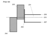
- the periphery of the hole collecting electrode 204 is a band schematically shown in FIG. It becomes a structure.
- reference numeral 202 is a non-doped intrinsic amorphous silicon ultrathin film
- reference numeral 203 is an n-type amorphous silicon film.
- Reference numeral 205 indicates the Fermi level
- reference numeral 206 indicates the lowest energy level of the conduction band
- reference numeral 207 indicates the highest energy level of the valence band.
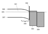
- the surface layer of the crystalline silicon 301 is doped with phosphorus atoms, and the portion is more than the normal n-type.
- the Fermi level 305 becomes a strong n-type approaching the energy level 306 at the lowest end of the conduction band, that is, n + type, as shown in FIG. 3, in the vicinity of the interface between the n-type crystalline silicon 301 and the amorphous silicon 302.
- the bands 306 and 307 on the crystalline silicon side are bent downward to facilitate movement of electrons to the electron collecting electrode 304.
- the holes are bounced away from the interface, and eventually, recombination of electrons and holes at the interface can be suppressed to improve the electron collection efficiency.
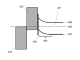
- boron atoms are doped in the surface layer of the crystalline silicon 401, and the portion is inverted to p-type, or Fermi
- bands 406 and 407 on the crystalline silicon side near the interface between the crystalline silicon 401 and the amorphous silicon 403 are on the upper side. Bends to facilitate moving the hole to the hole collection electrode 404.
- electrons are bounced away from the interface, and eventually, recombination of electrons and holes at the interface can be suppressed to improve the hole collection efficiency.
- the method of introducing phosphorus or boron into the crystalline silicon surface layer at a low temperature of 350 ° C. or less that can prevent the deterioration of the crystalline silicon itself is As a conventional technique, for example, there is a method of exposing crystalline silicon to a plasma-decomposed species, but technical problems to be overcome such as the upper surface of crystalline silicon becoming rough due to plasma damage are simultaneously presented. It was.
- an object of the present invention is to provide a heterojunction solar cell having a structure capable of dramatically suppressing the upper surface recombination of carriers and improving efficiency with respect to crystalline silicon, and a method for manufacturing the same. With the goal.
- the present invention provides a metal catalyst wire in which a layer doped with phosphorus or boron is formed in a very shallow region of the crystalline silicon surface layer, and a source gas containing phosphorus or boron such as phosphine or diborane is heated to 1,000 ° C. or higher.
- a new method of forming crystal silicon at a low temperature of 350 ° C. or less by exposing the crystalline silicon to the seeds produced by contact with the substrate and solved the above technical problem.
- this new method is referred to as “Cat-doping method”.
- the heterojunction solar cell of the present invention is a solar cell in which an amorphous silicon thin film is heterojunction to a crystalline silicon substrate, and the crystalline silicon substrate is doped with phosphorus in the extreme surface layer within a depth of 10 nanometers. Either a phosphorus-doped layer is formed, or the crystalline silicon substrate has a boron-doped layer in which boron is doped on the extreme surface layer within a depth of 10 nanometers, or both. It is characterized by.
- the method for producing a heterojunction solar cell is a method for producing a solar cell in which an amorphous silicon thin film is heterojunction to a crystalline silicon substrate, and is a metal catalyst body heated with a source gas containing phosphorus such as phosphine Exposing the crystalline silicon substrate to a seed produced by contact with a wire at a low temperature of 350 ° C. or less to form a phosphorus-doped layer by doping phosphorus into the extreme surface layer within a depth of 10 nanometers or diborane Boron on the extreme surface layer within a depth of 10 nanometers by exposing the crystalline silicon substrate at a low temperature of 350 ° C. or less to seeds produced by contact with a metal catalyst body wire heated with a source gas containing boron, etc. It is characterized in that either or both of the processes are performed by forming a boron-doped layer by doping.
- the electron and hole collection efficiency can be improved by suppressing recombination of electrons and holes at the interface of the heterojunction. Further, there is no problem that the upper surface of the crystalline silicon is rough.
- an interface transition layer is formed at the interface between the crystalline silicon substrate and the intrinsic amorphous silicon thin film, and the thickness of the interface transition layer is 0.6 nanometer or less. It is characterized by that.
- the method of manufacturing a heterojunction solar cell according to the present invention includes interfacial transition to the interface between the crystalline silicon substrate and the intrinsic amorphous silicon thin film by the action of either or both of the phosphorus-doped layer and the boron-doped layer. A layer is formed, and the thickness of the interface transition layer is 0.6 nanometer or less.
- the thickness of the interface transition layer is thin, the substantial area of the interface is reduced, recombination at the interface is suppressed, and the entire minority carrier lifetime is extended.
- the phosphorus-doped layer is formed on the upper surface side of the crystalline silicon substrate, the intrinsic amorphous silicon layer is laminated on the phosphorus-doped layer, and the intrinsic amorphous silicon layer
- the n-type amorphous silicon layer is laminated to form an electron collecting electrode, and the boron-doped layer is formed on the lower surface side of the crystalline silicon substrate, and the intrinsic amorphous layer is formed on the boron-doped layer.
- a silicon layer is laminated, and a hole collecting electrode is formed by laminating a p-type amorphous silicon layer on the intrinsic amorphous silicon layer.
- the method of manufacturing a heterojunction solar cell according to the present invention includes forming the phosphorus-doped layer on the upper surface side of the crystalline silicon substrate, and applying the intrinsic amorphous silicon layer to the phosphorus-doped layer by catalytic chemical vapor deposition. And laminating an n-type amorphous silicon layer on the intrinsic amorphous silicon layer to form an electron collecting electrode, and forming the boron-doped layer on the lower surface side of the crystalline silicon substrate. A hole collecting electrode is formed after laminating an intrinsic amorphous silicon layer on the doped layer and laminating a p-type amorphous silicon layer on the intrinsic amorphous silicon layer.
- the phosphorus-doped layer is formed on the upper surface side of the crystalline silicon substrate, the intrinsic amorphous silicon layer is laminated on the phosphorus-doped layer, and the intrinsic amorphous silicon layer
- An n-type amorphous silicon layer is laminated, a transparent conductive film is formed on the n-type amorphous silicon layer, a silicon nitride film is formed on the transparent conductive film, and pores are formed in the silicon nitride film at predetermined intervals.
- the electron collecting electrode is formed at the position of the pore group, and the boron doped layer is formed on the lower surface side of the crystalline silicon substrate, and the boron doped layer is intrinsic.
- An amorphous silicon layer is laminated, a p-type amorphous silicon layer is laminated on the intrinsic amorphous silicon layer, and the p-type amorphous silicon layer is laminated.
- a transparent conductive film is formed in the con layer, a silicon nitride film is formed under the transparent conductive film, pores are opened in the silicon nitride film at predetermined intervals, and a hole collecting electrode is formed at the position of the pore group It is characterized by being.
- the method of manufacturing a heterojunction solar cell according to the present invention includes forming the phosphorus-doped layer on the upper surface side of the crystalline silicon substrate, and applying the intrinsic amorphous silicon layer to the phosphorus-doped layer by catalytic chemical vapor deposition.
- a transparent conductive film is formed on the silicon layer, a silicon nitride film is formed under the transparent conductive film, pores are opened in the silicon nitride film at predetermined intervals, and hole collecting electrodes are formed at the positions of the pore groups. It is characterized by that.
- the phosphorus-doped layer is formed on the upper surface side of the crystalline silicon substrate, the silicon nitride film is formed on the phosphorus-doped layer, and The phosphorus-doped layer and the boron-doped layer are formed at a predetermined interval on the lower surface side of the crystalline silicon substrate, and the intrinsic amorphous silicon layer is laminated on the phosphorus-doped layer and the boron-doped layer.
- An n-type amorphous silicon layer is laminated immediately below the phosphorus-doped layer, a transparent conductive film is formed on the n-type amorphous silicon layer, and an electron collecting electrode is formed under the transparent conductive film.
- a p-type amorphous silicon layer is laminated immediately below the boron-doped layer, and a transparent conductive film is formed on the p-type amorphous silicon layer. Characterized in that the hole collecting electrode under the transparent conductive film is formed.
- the phosphorus-doped layer is formed on the upper surface side of the crystalline silicon substrate, and a silicon nitride film is formed on the phosphorus-doped layer by catalytic chemical vapor deposition.
- a p-type amorphous silicon layer is laminated immediately below the boron-doped layer, a transparent conductive film is formed on the p-type amorphous silicon layer, and the transparent conductive layer is formed. And forming a hole collecting electrode under the membrane.
- the phosphorus-doped layer is formed on the upper surface side of the crystalline silicon substrate, the silicon nitride film is formed on the phosphorus-doped layer, and The phosphorus-doped layer and the boron-doped layer are formed at a predetermined interval on the lower surface side of the crystalline silicon substrate, and the intrinsic amorphous silicon layer is laminated on the phosphorus-doped layer and the boron-doped layer.
- a silicon nitride film is formed under the intrinsic amorphous silicon layer, and pores are opened in the silicon nitride film at a predetermined interval, at a position immediately below the phosphorus-doped layer in the pore group position.
- n-type amorphous silicon layer is laminated, a transparent conductive film is formed on the n-type amorphous silicon layer, and an electron collecting electrode is formed below the transparent conductive film.
- a p-type amorphous silicon layer is laminated immediately below the boron-doped layer, a transparent conductive film is formed on the p-type amorphous silicon layer, and a hole collecting electrode is formed under the transparent conductive film It is characterized by being.
- the phosphorus-doped layer is formed on the upper surface side of the crystalline silicon substrate, and a silicon nitride film is formed on the phosphorus-doped layer by catalytic chemical vapor deposition. And forming the phosphorus-doped layer and the boron-doped layer at a predetermined interval on the lower surface side of the crystalline silicon substrate, and forming an intrinsic amorphous silicon layer on the phosphorus-doped layer and the boron-doped layer.
- n-type amorphous silicon layer is laminated, a transparent conductive film is formed on the n-type amorphous silicon layer, an electron collecting electrode is formed under the transparent conductive film, and the A p-type amorphous silicon layer is formed immediately below the doped layer, a transparent conductive film is formed on the p-type amorphous silicon layer, and a hole collecting electrode is formed under the transparent conductive film.
- either or both of the phosphorus-doped layer and the boron-doped layer are layers doped at a low temperature of 350 ° C. or less, and the intrinsic amorphous silicon thin film is formed by catalytic chemical vapor deposition. It is the thin film formed by these.
- the film is deposited by the Cat-CVD method, defects are not introduced into the upper surface of the crystalline silicon substrate, and a high-quality solar cell is obtained.
- the thickness of the silicon substrate is set to 100 ⁇ m or less, the recombination of electrons and holes on the upper surface of the crystalline silicon is suppressed to the limit without deteriorating its characteristics, so that high efficiency is achieved. Will get.
- the doped layer is formed using a seed produced by decomposition of the doping gas in the Cat-CVD apparatus by catalytic decomposition with the catalytic body, and is doped at low temperature. Even when the thickness of the silicon substrate is 100 ⁇ m or less, the recombination of electrons and holes on the upper surface of the crystalline silicon is suppressed to the limit without deteriorating its characteristics, and it is easy to obtain high efficiency.
- the intrinsic amorphous silicon thin film and the silicon nitride film are both formed by a Cat-CVD method, the silicon nitride film on the lower surface side of the silicon substrate is masked, and the silicon nitride film is etched. It is characterized in that pores are opened at predetermined intervals, and electrode groups are formed at the positions of the pore groups.
- a laminated film of amorphous silicon and silicon nitride capable of dramatically suppressing the upper surface recombination of carriers with respect to a crystalline silicon substrate such as crystalline silicon or polycrystalline silicon, and also a defect on the upper surface of silicon.
- a laminated film made by using a Cat-CVD method that can be deposited without introducing, recombination of electrons and holes generated by sunlight can be suppressed.
- the silicon nitride film on the lower surface side of the silicon substrate is opened by pores at predetermined intervals by etching, and an electrode group is formed at the position of the pore group. It becomes the structure which protects most from the outside air.
- the present invention is characterized in that the electrode group is formed by a liquid coating method.
- the electrode group is formed by a low temperature process, high efficiency can be obtained.
- liquid application method examples include inkjet and spin coating.
- the liquid application method is also called a liquid process.
- a liquid containing conductive metal fine particles or fine particles on which a conductive metal film is formed is applied, and a treatment such as H atom treatment is performed to form electrodes.
- the present invention is characterized in that the silicon substrate is n-type crystalline silicon and the light receiving surface of the silicon substrate has a texture structure.
- the present invention is characterized in that, as the electrode group, first electrode groups for collecting electrons and second electrode groups for collecting holes are alternately arranged.
- the electrode group is arranged in a well-balanced manner, it is easy to obtain high efficiency.
- the number of the first electrode group and the second electrode group may be different or the same.
- the silicon nitride film on the light receiving surface side of the silicon substrate is a base silicon nitride film on the side in contact with the amorphous silicon thin film, and the base such as silicon oxide, silicon oxynitride, or aluminum oxide is formed thereon. It is characterized by a structure in which films containing oxygen having a refractive index lower than that of a silicon nitride film are stacked.
- the solar cell element since the silicon nitride film is a laminated film having a different refractive index, the solar cell element has a wide band in which the absorption region of sunlight is expanded even for a short wavelength.
- the amorphous silicon thin film contains impurities such as hydrogen, oxygen, nitrogen, carbon, germanium, tin, boron, phosphorus, etc. while having amorphous silicon as a skeleton, and the silicon nitride
- the film is characterized by containing silicon nitride as a skeleton and impurities such as hydrogen, oxygen and carbon.
- a highly efficient solar cell can be obtained from an existing production line.
- the impurity may be an unavoidable impurity or may be an impurity that is actively contained.
- the content rate of the said impurity is set arbitrarily.
- the heterojunction solar cell of the present invention it is possible to suppress the recombination of electrons and holes at the interface of the heterojunction and improve the collection efficiency of electrons and holes.
- the thickness of the interface transition layer is thin, the substantial area of the interface is reduced, recombination at the interface is suppressed, and the entire minority carrier lifetime is extended.
- the film is deposited by the Cat-CVD method, defects are not introduced into the upper surface of the crystalline silicon substrate, and a high-quality solar cell is obtained. According to the present invention, a high-efficiency and high-quality solar cell is obtained.
- FIG. 3 is a cross-sectional structure diagram schematically showing a heterojunction solar cell 3 of the present invention. In order to compare a prior art with this invention, it is the graph which compared the power generation characteristic of the solar cell.
- FIG. 5 shows a sample 500 of the prior art, in which an n-type amorphous silicon film 503 is formed at a heterojunction between an n-type crystalline silicon substrate 501 and a non-doped intrinsic amorphous silicon ultrathin film 502 and crystallized by an electron collecting electrode 504. Covers both sides of the silicon substrate.
- FIG. 5 shows a sample 500 of the prior art, in which an n-type amorphous silicon film 503 is formed at a heterojunction between an n-type crystalline silicon substrate 501 and a non-doped intrinsic amorphous silicon ultrathin film 502 and crystallized by an electron collecting electrode 504. Covers both sides of the silicon substrate.
- FIG. 5 shows a sample 500 of the prior art, in which an n-type amorphous silicon film 503 is formed at a heterojunction between an n-type crystalline silicon substrate 501 and a non-doped intrinsic amorphous silicon ultrathin film 502 and crystallized by an
- FIG. 6 shows a sample 600 according to the present invention, in which phosphorus is cat-doped on the surface layer of an n-type crystalline silicon substrate 601 to form a phosphorus-doped layer 608, and then an intrinsic amorphous silicon ultrathin film 602 and an n-type amorphous silicon.
- a 603 film is deposited and the electron collecting electrode 604 covers both sides of the crystalline silicon substrate.
- Minority carrier lifetime was estimated by the microwave photoconductive decay method, and the result is shown as a function of processing gas pressure during Cat-doping as shown in FIG.
- a phosphorus-doped layer doped with phosphorus atoms in the crystalline silicon surface layer according to the present invention By having a phosphorus-doped layer doped with phosphorus atoms in the crystalline silicon surface layer according to the present invention, recombination at the interface between crystalline silicon and amorphous silicon of electrons and holes is suppressed, so In the undoped sample 500, the minority carrier lifetime was only 200 microseconds, whereas in the sample 600 in which the Cat-doping layer 608 is formed on the crystalline silicon surface layer, the minority carrier lifetime was 1.8 milliseconds.
- FIG. 7 shows a dramatic improvement. That is, the effect of the present invention is also apparent from FIG.
- the Cat-CVD method is employed as a method for preventing plasma damage on the upper surface of the crystalline silicon substrate as in the conventional method for the deposition of amorphous silicon.
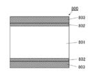
- a sample 800 shown in FIG. 8 has a structure in which intrinsic amorphous silicon 802 having a thickness of about 10 nanometers is deposited on both front and back surfaces of an n-type crystalline silicon substrate 801, and a silicon nitride film 803 is further deposited thereon. The minority carrier lifetime of the sample was measured.
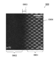
- FIG. 9A shows an electron microscope image when observed with a high-resolution transmission electron microscope. In this image, even the arrangement of crystalline silicon atoms can be clearly seen.
- reference numeral 904 is an image of a silicon atom pair.
- Reference numeral 903 denotes an interface transition layer between the n-type crystalline silicon 901 and the amorphous silicon 902.
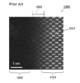
- FIG. 10A shows an electron microscope image when observed with a 0.08 nanometer ultrahigh resolution transmission electron microscope.
- Reference numeral 1004 in FIG. 10A is an image of a silicon atom pair.
- Reference numeral 1003 denotes an interface transition layer between the n-type crystalline silicon 901 and the amorphous silicon 902. 9A and 10A, the sample 900 using the Cat-CVD amorphous silicon film according to the present invention shown in FIG.
- the sample 1000 using the PECVD amorphous silicon film of the prior art shown in FIG. 10A has an interface between amorphous silicon and crystalline silicon.
- the width of the transition layer 1003 is about 1.0 nanometer.
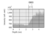
- FIG. 9B is a signal obtained when the atomic arrangement of crystalline silicon is or is not periodic in an electron microscope image when the sample 900 of FIG. 9A is observed with an ultrahigh resolution transmission electron microscope according to the present invention. It is the graph which estimated the value by making into the width
- the vertical axis of the graph represents the signal intensity with respect to crystalline silicon, and the horizontal axis of the graph represents the depth from the surface layer of crystalline silicon.
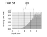
- FIG. 10B shows the case where the atomic arrangement of crystalline silicon is periodic in the electron microscope image when the sample 1000 formed by the plasma assisted CVD method of the prior art is observed with an ultrahigh resolution transmission electron microscope.
- FIG. 10B shows the case where the atomic arrangement of crystalline silicon is periodic in the electron microscope image when the sample 1000 formed by the plasma assisted CVD method of the prior art is observed with an ultrahigh resolution transmission electron microscope.
- FIG. 6 is a graph in which the value obtained by estimating the width of the transition layer as the width of the change in the signal intensity difference is estimated.
- the sample 900 using the Cat-CVD amorphous silicon film according to the present invention shown in FIG. 9B has a width of the transition layer 903 at the interface between the amorphous silicon and the crystalline silicon.
- the sample 1000 using the prior art PECVD amorphous silicon film shown in FIG. 10B has a width of the transition layer 1003 at the interface between amorphous silicon and crystalline silicon of 1.8 nanometers. become.
- the present invention aims to reduce the price of a crystalline silicon solar cell by reducing the amount of crystalline silicon used as a raw material by reducing the thickness of the crystalline silicon substrate, improving the electron collecting electrode and the hole collecting electrode. Therefore, it is effective to increase the electron collection efficiency at the electron collection electrode and the hole collection efficiency at the hole collection electrode, and as a result, improve the energy conversion efficiency. Furthermore, as a means for realizing the present invention, the manufacturing cost is further reduced by using the Cat-CVD method, which is about 10 times higher than the conventional PECVD method, for the deposition of amorphous silicon film. Also has utility.
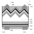
- FIG. 11 shows an example of the structure of the solar cell 1 that embodies the present invention.
- the sunlight irradiation surface has a structure that prevents reflection of sunlight on the upper surface as much as possible by utilizing irregular reflection of light.
- the electron collection electrode 1108 and the hole collection electrode 1108 are formed on the sunlight irradiation surface and the lower surface, respectively.
- an n-type crystalline silicon substrate 1101 is used.
- Phosphorus atoms are introduced into the surface layer of the crystalline silicon 1101 by a Cat-doping method at a low temperature of 80 ° C. to form a phosphorus-doped layer 1102 whose surface layer portion is changed to n + type, and a thickness of several nanometers is formed thereon.
- An intrinsic amorphous silicon film 1104 and an n-type amorphous silicon film 1105 having a thickness of 10 to 20 nanometers are sequentially deposited by Cat-CVD, and a transparent conductive film 1107 is further deposited and a metal such as silver is deposited thereon.
- the electron collecting electrode 1108 is deposited.
- a transparent conductive film 1107 is inserted between the n-type amorphous silicon film 1105 and the metal electrode 1108. This is because the transparent conductive film 1107 prevents the last deposited metal 1108 from diffusing into the amorphous silicon layer 1106.
- reference numeral 1109 denotes a silicon nitride film.
- boron atoms are introduced into the surface layer of the crystalline silicon 1101 by a Cat-doping method at a low temperature of 80 ° C., and the surface layer portion is changed to p-type.
- a doping layer 1103 is formed, and an intrinsic amorphous silicon film 1104 having a thickness of several nanometers and an n-type amorphous silicon film 1105 having a thickness of 10 to 20 nanometers are sequentially deposited by Cat-CVD, respectively,
- the hole collecting electrode 1118 is formed by depositing a metal such as silver on the transparent conductive film 1107.
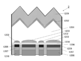
- FIG. 12 shows an example of the structure of the solar cell 2 that embodies the present invention.
- the sunlight irradiation surface has a structure that prevents reflection of sunlight on the upper surface as much as possible by utilizing irregular reflection of light.
- n-type crystalline silicon substrate 1201 is used. Phosphorus atoms are introduced into the surface layer of the crystalline silicon 1201 by a Cat-doping method at a low temperature of 80 ° C. to form a phosphorus-doped layer 1202 in which the surface layer portion is changed to n + type, on which a thickness of several nanometers is formed.
- Intrinsic amorphous silicon film 1204 and n-type amorphous silicon film 1205 having a thickness of 10 to 20 nanometers are sequentially deposited by Cat-CVD method, and further, a transparent conductive film 1207 is deposited and a metal such as silver is deposited thereon.
- the electron collecting electrode 1208 is deposited.
- a transparent conductive film 1207 is inserted between the n-type amorphous silicon film 1205 and the metal electrode 1208. This is because the transparent conductive film 1207 prevents the metal 1208 deposited last from diffusing into the amorphous silicon layer 1206.
- reference numeral 1209 denotes a silicon nitride film.
- boron atoms are introduced into the surface layer of the crystalline silicon 1201 by a Cat-doping method at a low temperature of 80 ° C., and the surface layer portion is changed to p-type.
- a doping layer 1203 is formed, and an intrinsic amorphous silicon film 1204 having a thickness of several nanometers and an n-type amorphous silicon film 1205 having a thickness of 10 to 20 nanometers are sequentially deposited thereon by Cat-CVD.
- a hole collecting electrode 1218 is formed by depositing a metal such as silver on the transparent conductive film 1207.
- the solar irradiation surface can be devised in various ways for efficiently capturing sunlight, so that the electrode disappears from the solar irradiation surface and the influence of the electrode shadow can be eliminated.
- this solar cell structure has great utility.
- FIG. 13 is a schematic diagram of an apparatus 1300 for performing Cat-doping according to the present invention.
- the apparatus itself is the same as the Cat-CVD apparatus.
- a stainless steel chamber 1301 having a diameter of about 30 centimeters and a height of about 30 centimeters is used, and the processing chamber is evacuated from a vacuum exhaust port 1302.
- a phosphine gas around a flow rate of 0.4 sccm (a flow rate in which the gas volume flowing per minute in terms of 1 atm is expressed in cc) is passed through the chamber 1301 from the gas inlet 1307 into the chamber. At this time, hydrogen gas with a flow rate of 10 to 20 sccm may be simultaneously supplied.
- the gas pressure is about 1 Pa to 2 Pa (hereinafter referred to as “Pa”).
- Crystalline silicon 1304 is placed on the sample holder 1303. Usually, in order not to contaminate the upper surface of the crystalline silicon 1304, the crystalline silicon 1304 is fixed only by its end surface, and is devised and fixed so as not to contact the upper surface of the sample holder 1303.
- the temperature of the crystalline silicon 1304 is kept at about 80 ° C.
- a catalyst body for decomposing phosphine gas a tungsten wire having a thickness of 0.5 millimeters and a length of about 2 meters is used as a catalyst wire 1305, and a zigzag is stretched while maintaining a distance Dcs from the sample at about 10 centimeters.
- This tungsten wire 1305 is energized and heated to keep the temperature at about 1,300 ° C.
- the time for Cat-doping by flowing phosphine gas is about 60 seconds, but this time can be appropriately changed. However, Cat-doping for a long time is not necessary, and a sufficient effect can be obtained even if it is shorter than 60 seconds.
- reference numeral 1306 denotes a gas jet shower head.
- the cat-doping of boron is the same as that of phosphorus-cat-doping using phosphine except that diborane is used instead of phosphine.
- FIG. 4 shows the result of observation of the distribution of phosphorus atoms in crystalline silicon by secondary ion mass spectrometry when phosphorus atoms are introduced into crystalline silicon at 80 ° C. substrate temperature by Cat-doping according to the present invention. It is shown in 14 graphs.
- the vertical axis of the graph is the density of phosphorus atoms
- the horizontal axis of the graph is the depth from the surface layer of crystalline silicon.
- the distribution of phosphorus atoms follows a complementary error function (denoted as “erfc”), which is a distribution seen during thermal diffusion when the doping gas concentration on the top surface is constant, and is only 80 ° C. at a low temperature. Is diffused into the crystalline silicon.
- erfc complementary error function
- Reference numeral 1402 is a complementary error function form.
- the value that the diffusion coefficient, the diffusion coefficient of the well-known phosphorus atom in the ordinary thermal diffusion obtained in experiments at high temperatures above 800 ° C. is obtained by extrapolating the simple 80 ° C., 10 -28 Compared to (micrometer) 2 / hour, it is nearly 10 20 times larger, which is a major feature of Cat-doping.
- the penetration depth of phosphorus atoms is as shallow as 10 nanometers or less, but is sufficient to bend the band on the top surface of crystalline silicon.
- reference numeral 1403 indicates the position of the upper surface of the crystalline silicon substrate, and reference numeral 1403 indicates the density distribution of phosphorus atoms measured by etching from the lower surface of the crystalline silicon substrate.
- intrinsic amorphous silicon, n-type and p-type amorphous silicon are sequentially deposited on a substrate in which phosphorus atoms and boron atoms are introduced into the crystalline silicon surface layer, and a transparent electrode and a metal electrode are further formed thereon.
- the solar cell 1 or 2 is limited to only the electron collecting electrode portion. As shown in FIG.
- a phosphorus-doped layer 1502 in which phosphorus atoms are cat-doped is formed on the layer, an intrinsic amorphous silicon film 1503 is deposited thereon, and an n-type amorphous silicon film 1504 is deposited to form a transparent electrode film 1506
- a silver electrode 1507 is formed, and an intrinsic amorphous silicon film 1503 is formed on the lower layer of the n-type crystalline silicon 1501. It is product, by depositing a p-type amorphous silicon film 1505 to form a transparent electrode film 1506 was fabricated solar cell 3 of the structure forming the silver electrode 1507. The characteristics of the solar cell 3 were compared with those of a conventional solar cell that does not include a Cat-doping layer.
- FIG. 16 shows a current-voltage characteristic of a solar cell 1602 of the prior art that does not include a Cat-doping phosphorus atomic layer and a solar cell 1601 of the present invention that includes a Cat-doping phosphorus atomic layer, that is, power generation of the solar cell. It is a comparison of characteristics.
- the solar cell in this case is a rudimentary one that is not subjected to any top surface processing for suppressing reflection of sunlight.
- Cat-Doping phosphorus atom layer of the present invention in crystalline silicon surface layer, the short-circuit current J SC of the solar cell, for electron collection efficiency of the electrode is increased, the conventional 1602 short-circuit current J SC 36.
- the present invention further improves the energy conversion efficiency of a solar cell having a heterojunction of amorphous silicon and crystalline silicon.
- the present invention is not limited to the embodiment described above.
- the amorphous silicon thin film and the silicon nitride film are described as being formed by the Cat-CVD method, but the present invention is not limited to this.
- the present invention can be modified as appropriate without departing from the spirit of the present invention.
- 1,2,3 Heterojunction solar cell of the present invention 901 crystalline silicon, 902 amorphous silicon, 903 Interface transition layer between amorphous silicon and crystalline silicon
Landscapes
- Photovoltaic Devices (AREA)
Abstract
L'invention aborde le problème de produire une cellule solaire à hétérojonction ayant une structure dans laquelle la recombinaison des porteurs sur la surface supérieure du silicium cristallin peut être considérablement inhibée et qui atteint une efficacité accrue. La présente invention réalise à cet effet une cellule solaire à hétérojonction qui est une cellule solaire dans laquelle un film mince en silicium amorphe intrinsèque a été lié par hétérojonction à un substrat en silicium cristallin. Le substrat en silicium cristallin possède une couche dopée formée par dopage d'une couche de surface extrême ayant une profondeur de 10 nanomètres ou moins avec du phosphore ou du bore. Selon une photomicrographie électronique obtenue lorsqu'un échantillon (900) a été examiné avec un microscope électronique à transmission, l'échantillon (900) ayant été produit en déposant un film en silicium amorphe intrinsèque (902) directement sur un substrat en silicium cristallin de type n (901) par un procédé de dépôt chimique en phase vapeur catalytique, l'épaisseur d'une couche de transition d'interface (903) entre le silicium cristallin de type n (901) et le silicium amorphe (902) est inférieure ou égale à 0,6 nanomètres.
Priority Applications (1)
| Application Number | Priority Date | Filing Date | Title |
|---|---|---|---|
| JP2016507447A JP6396425B2 (ja) | 2014-03-14 | 2015-02-27 | ヘテロ接合太陽電池とその製造方法 |
Applications Claiming Priority (2)
| Application Number | Priority Date | Filing Date | Title |
|---|---|---|---|
| JP2014-051160 | 2014-03-14 | ||
| JP2014051160 | 2014-03-14 |
Publications (1)
| Publication Number | Publication Date |
|---|---|
| WO2015137152A1 true WO2015137152A1 (fr) | 2015-09-17 |
Family
ID=54071600
Family Applications (1)
| Application Number | Title | Priority Date | Filing Date |
|---|---|---|---|
| PCT/JP2015/055772 Ceased WO2015137152A1 (fr) | 2014-03-14 | 2015-02-27 | Cellule solaire à hétérojonction et son procédé de production |
Country Status (3)
| Country | Link |
|---|---|
| JP (1) | JP6396425B2 (fr) |
| TW (1) | TW201535761A (fr) |
| WO (1) | WO2015137152A1 (fr) |
Cited By (9)
| Publication number | Priority date | Publication date | Assignee | Title |
|---|---|---|---|---|
| JP2018121053A (ja) * | 2017-01-26 | 2018-08-02 | エルジー エレクトロニクス インコーポレイティド | 太陽電池及びその製造方法 |
| CN109004053A (zh) * | 2017-06-06 | 2018-12-14 | 中国科学院上海微系统与信息技术研究所 | 双面受光的晶体硅/薄膜硅异质结太阳电池及制作方法 |
| CN110643971A (zh) * | 2019-09-27 | 2020-01-03 | 上海理想万里晖薄膜设备有限公司 | 用于制造异质结太阳能电池的cvd设备及其镀膜方法 |
| CN114005886A (zh) * | 2021-10-29 | 2022-02-01 | 苏州光汇新能源科技有限公司 | 一种适用于室内发电的硅异质结太阳电池结构及其制备方法 |
| CN114497288A (zh) * | 2022-01-26 | 2022-05-13 | 中节能太阳能科技(镇江)有限公司 | 栅线嵌入选择性重掺杂区域的异质结太阳能电池制造方法 |
| CN114497260A (zh) * | 2022-02-08 | 2022-05-13 | 上海理想万里晖薄膜设备有限公司 | 用于制造异质结太阳能电池的方法及异质结太阳能电池 |
| CN114566561A (zh) * | 2020-11-27 | 2022-05-31 | 嘉兴阿特斯技术研究院有限公司 | 异质结太阳能电池及其制作方法 |
| CN116247111A (zh) * | 2021-12-07 | 2023-06-09 | 嘉兴阿特斯技术研究院有限公司 | 太阳能电池及其制备方法 |
| CN116913991A (zh) * | 2023-08-01 | 2023-10-20 | 天合光能股份有限公司 | 异质结太阳能电池及其制备方法、光伏组件以及光伏系统 |
Families Citing this family (1)
| Publication number | Priority date | Publication date | Assignee | Title |
|---|---|---|---|---|
| CN108831967B (zh) * | 2018-06-25 | 2019-10-29 | 江苏悦阳光伏科技有限公司 | 一种新型hit太阳能电池及其制备方法 |
Citations (3)
| Publication number | Priority date | Publication date | Assignee | Title |
|---|---|---|---|---|
| JP2000058885A (ja) * | 1998-08-03 | 2000-02-25 | Sanyo Electric Co Ltd | 太陽電池及びその製造方法 |
| JP2011146528A (ja) * | 2010-01-14 | 2011-07-28 | Kaneka Corp | 多結晶シリコン系太陽電池およびその製造方法 |
| WO2013179529A1 (fr) * | 2012-05-30 | 2013-12-05 | パナソニック株式会社 | Cellule solaire |
-
2015
- 2015-02-27 WO PCT/JP2015/055772 patent/WO2015137152A1/fr not_active Ceased
- 2015-02-27 JP JP2016507447A patent/JP6396425B2/ja not_active Expired - Fee Related
- 2015-03-13 TW TW104108169A patent/TW201535761A/zh unknown
Patent Citations (3)
| Publication number | Priority date | Publication date | Assignee | Title |
|---|---|---|---|---|
| JP2000058885A (ja) * | 1998-08-03 | 2000-02-25 | Sanyo Electric Co Ltd | 太陽電池及びその製造方法 |
| JP2011146528A (ja) * | 2010-01-14 | 2011-07-28 | Kaneka Corp | 多結晶シリコン系太陽電池およびその製造方法 |
| WO2013179529A1 (fr) * | 2012-05-30 | 2013-12-05 | パナソニック株式会社 | Cellule solaire |
Non-Patent Citations (3)
| Title |
|---|
| HIDEKI MATSUMURA ET AL.: "Cat-doping: Novel method for phosphorus and boron shallow doping in crystalline silicon at 80°C", JOURNAL OF APPLIED PHYSICS, vol. 116, no. 11, September 2014 (2014-09-01), pages 114502 - 1 114502-10, XP012191053, ISSN: 0021-8979 * |
| KEISUKE OHDAIRA ET AL.: "Surface treatment of crystalline silicon realizing extremely low surface recombination velocity using catalytically generated radicals", PHOTOVOLTAIC SPECIALISTS CONFERENCE (PVSC), 2010 35TH IEEE, 2010, pages 003220 - 003222, XP031786191 * |
| TARO HAYAKAWA ET AL.: "Extremely low recombination velocity on crystalline silicon surfaces realized by low-temperature impurity doping in Cat-CVD technology", THIN SOLID FILMS, vol. 519, no. Iss.14, 2011, pages 4466 - 4468, XP055223743, ISSN: 0040-6090, DOI: doi:10.1016/j.tsf.2011.01.301 * |
Cited By (12)
| Publication number | Priority date | Publication date | Assignee | Title |
|---|---|---|---|---|
| JP2018121053A (ja) * | 2017-01-26 | 2018-08-02 | エルジー エレクトロニクス インコーポレイティド | 太陽電池及びその製造方法 |
| CN109004053A (zh) * | 2017-06-06 | 2018-12-14 | 中国科学院上海微系统与信息技术研究所 | 双面受光的晶体硅/薄膜硅异质结太阳电池及制作方法 |
| CN109004053B (zh) * | 2017-06-06 | 2024-03-29 | 通威太阳能(成都)有限公司 | 双面受光的晶体硅/薄膜硅异质结太阳电池及制作方法 |
| CN110643971A (zh) * | 2019-09-27 | 2020-01-03 | 上海理想万里晖薄膜设备有限公司 | 用于制造异质结太阳能电池的cvd设备及其镀膜方法 |
| CN114566561A (zh) * | 2020-11-27 | 2022-05-31 | 嘉兴阿特斯技术研究院有限公司 | 异质结太阳能电池及其制作方法 |
| CN114005886A (zh) * | 2021-10-29 | 2022-02-01 | 苏州光汇新能源科技有限公司 | 一种适用于室内发电的硅异质结太阳电池结构及其制备方法 |
| CN114005886B (zh) * | 2021-10-29 | 2024-01-09 | 苏州光汇新能源科技有限公司 | 一种适用于室内发电的硅异质结太阳电池结构及其制备方法 |
| CN116247111A (zh) * | 2021-12-07 | 2023-06-09 | 嘉兴阿特斯技术研究院有限公司 | 太阳能电池及其制备方法 |
| CN114497288A (zh) * | 2022-01-26 | 2022-05-13 | 中节能太阳能科技(镇江)有限公司 | 栅线嵌入选择性重掺杂区域的异质结太阳能电池制造方法 |
| CN114497260A (zh) * | 2022-02-08 | 2022-05-13 | 上海理想万里晖薄膜设备有限公司 | 用于制造异质结太阳能电池的方法及异质结太阳能电池 |
| CN114497260B (zh) * | 2022-02-08 | 2024-01-09 | 理想万里晖半导体设备(上海)股份有限公司 | 用于制造异质结太阳能电池的方法及异质结太阳能电池 |
| CN116913991A (zh) * | 2023-08-01 | 2023-10-20 | 天合光能股份有限公司 | 异质结太阳能电池及其制备方法、光伏组件以及光伏系统 |
Also Published As
| Publication number | Publication date |
|---|---|
| TW201535761A (zh) | 2015-09-16 |
| JP6396425B2 (ja) | 2018-09-26 |
| JPWO2015137152A1 (ja) | 2017-04-06 |
Similar Documents
| Publication | Publication Date | Title |
|---|---|---|
| JP6396425B2 (ja) | ヘテロ接合太陽電池とその製造方法 | |
| US11605750B2 (en) | Solar cell having an emitter region with wide bandgap semiconductor material | |
| Sharma et al. | Nanocrystalline silicon thin film growth and application for silicon heterojunction solar cells: a short review | |
| JP5456168B2 (ja) | 光電変換装置の製造方法 | |
| US9871161B2 (en) | Method for making crystalline silicon-based solar cell, and method for making solar cell module | |
| CN102656707B (zh) | 薄膜硅叠层太阳能电池及其制造方法 | |
| US20130269767A1 (en) | Method of coating a substrate for manufacturing a solar cell | |
| JP2007281156A (ja) | 裏面電極型半導体へテロ接合太陽電池ならびにその製造方法と製造装置 | |
| CN103748692A (zh) | 太阳能电池以及用于制造太阳能电池的方法 | |
| Chen et al. | Optimized n-type amorphous silicon window layers via hydrogen dilution for silicon heterojunction solar cells by catalytic chemical vapor deposition | |
| TWI790245B (zh) | 光電轉換裝置之製造方法 | |
| TW201201396A (en) | Method for manufacturing a solar panel | |
| CN103430326A (zh) | 微晶PIN结的SiOxN型层 | |
| JP4674956B2 (ja) | 薄膜太陽電池およびその製造方法 | |
| CN118867057B (zh) | 太阳能电池及其制备方法 | |
| JP5136066B2 (ja) | 光起電力素子およびその製造方法 | |
| JP2014007198A (ja) | 結晶シリコン系光電変換装置およびその製造方法 | |
| JP2009170507A (ja) | 光起電力素子およびその製造方法 |
Legal Events
| Date | Code | Title | Description |
|---|---|---|---|
| 121 | Ep: the epo has been informed by wipo that ep was designated in this application |
Ref document number: 15761228 Country of ref document: EP Kind code of ref document: A1 |
|
| DPE1 | Request for preliminary examination filed after expiration of 19th month from priority date (pct application filed from 20040101) | ||
| ENP | Entry into the national phase |
Ref document number: 2016507447 Country of ref document: JP Kind code of ref document: A |
|
| NENP | Non-entry into the national phase |
Ref country code: DE |
|
| 122 | Ep: pct application non-entry in european phase |
Ref document number: 15761228 Country of ref document: EP Kind code of ref document: A1 |