WO2015141015A9 - 基本素子 - Google Patents
基本素子 Download PDFInfo
- Publication number
- WO2015141015A9 WO2015141015A9 PCT/JP2014/059380 JP2014059380W WO2015141015A9 WO 2015141015 A9 WO2015141015 A9 WO 2015141015A9 JP 2014059380 W JP2014059380 W JP 2014059380W WO 2015141015 A9 WO2015141015 A9 WO 2015141015A9
- Authority
- WO
- WIPO (PCT)
- Prior art keywords
- particle
- particles
- energy
- ratio
- absorption
- Prior art date
- Legal status (The legal status is an assumption and is not a legal conclusion. Google has not performed a legal analysis and makes no representation as to the accuracy of the status listed.)
- Ceased
Links
Images


Classifications
-
- H—ELECTRICITY
- H01—ELECTRIC ELEMENTS
- H01J—ELECTRIC DISCHARGE TUBES OR DISCHARGE LAMPS
- H01J1/00—Details of electrodes, of magnetic control means, of screens, or of the mounting or spacing thereof, common to two or more basic types of discharge tubes or lamps
- H01J1/02—Main electrodes
- H01J1/30—Cold cathodes, e.g. field-emissive cathode
- H01J1/304—Field-emissive cathodes
- H01J1/3042—Field-emissive cathodes microengineered, e.g. Spindt-type
- H01J1/3044—Point emitters
-
- H—ELECTRICITY
- H05—ELECTRIC TECHNIQUES NOT OTHERWISE PROVIDED FOR
- H05H—PLASMA TECHNIQUE; PRODUCTION OF ACCELERATED ELECTRICALLY-CHARGED PARTICLES OR OF NEUTRONS; PRODUCTION OR ACCELERATION OF NEUTRAL MOLECULAR OR ATOMIC BEAMS
- H05H3/00—Production or acceleration of neutral particle beams, e.g. molecular or atomic beams
- H05H3/02—Molecular or atomic-beam generation, e.g. resonant beam generation
-
- H—ELECTRICITY
- H01—ELECTRIC ELEMENTS
- H01J—ELECTRIC DISCHARGE TUBES OR DISCHARGE LAMPS
- H01J37/00—Discharge tubes with provision for introducing objects or material to be exposed to the discharge, e.g. for the purpose of examination or processing thereof
- H01J37/02—Details
- H01J37/04—Arrangements of electrodes and associated parts for generating or controlling the discharge, e.g. electron-optical arrangement or ion-optical arrangement
- H01J37/06—Electron sources; Electron guns
- H01J37/073—Electron guns using field emission, photo emission, or secondary emission electron sources
-
- B—PERFORMING OPERATIONS; TRANSPORTING
- B82—NANOTECHNOLOGY
- B82Y—SPECIFIC USES OR APPLICATIONS OF NANOSTRUCTURES; MEASUREMENT OR ANALYSIS OF NANOSTRUCTURES; MANUFACTURE OR TREATMENT OF NANOSTRUCTURES
- B82Y30/00—Nanotechnology for materials or surface science, e.g. nanocomposites
-
- H—ELECTRICITY
- H01—ELECTRIC ELEMENTS
- H01J—ELECTRIC DISCHARGE TUBES OR DISCHARGE LAMPS
- H01J2237/00—Discharge tubes exposing object to beam, e.g. for analysis treatment, etching, imaging
- H01J2237/06—Sources
- H01J2237/063—Electron sources
- H01J2237/06383—Spin polarised electron sources
Definitions
- the present invention relates to a basic element having a particle emission / absorption source containing electromagnetic waves, electrons, holes, atoms / molecules, etc., and particles entering / exiting between other basic elements, interaction between these particles, chemical reaction, etc.
- Modifiers that allow time-varying mechanical / electromagnetic forces to the particle moving part face the emission / absorption edge of the basic element or are in the space created by the emission / absorption edge of one or more basic elements, Emission and absorption of low-energy particles that suppress the influence on the S / N ratio due to the steric structure and lattice of the constituent material of the particle moving part between the absorption edges and their three-dimensional structure and lattice, and the heat of the device
- the present invention relates to a basic element to be controlled and an apparatus, module, and system constructed from the plurality of basic elements.
- a beam of electromagnetic waves, particles, etc. (hereinafter abbreviated as a generic name when no particle is specified) is irradiated to the sample to analyze the physicochemical structure of the sample or to irradiate the material. It is used for physical or chemical processing or as an energy source.
- an electron beam is used in a scanning electron microscope, a transmission electron microscope, an electron beam exposure apparatus, a thermionic emission electron gun, a field emission electron gun, and the like.
- the electron emission area can be reduced, the cathode tip spherical surface having a radius of 0.4 ⁇ m is heated to 1800 K, and the electric field applied to the electron emission surface is ⁇ 10 8 V / m. It becomes a high-intensity electron beam about three orders of magnitude higher than a gun.
- the electric field (Schottky) emission type gun requires heating of the cathode, the Schottky shield, the first and second anodes, and the cathode.
- a pierce-type electron gun structure having a concave-shaped cathode having self-focusing characteristics is used, the electron flow is focused as a laminar flow.
- Non-patent document 1 Non-patent document 2
- Non-patent Document 3 in the electric field (Schottky) emission electron gun using single-walled or multi-walled carbon nanotubes, the height from the cathode is 1.6 ⁇ m and the radius is 7.5 nm.
- Particle beams are used for physical and chemical processing, and include molecular beam epitaxy, ion beam lithography, and ion implantation. With a focused ion beam, the target material can be processed in nano-order. It is also used to excite gas, control discharge, and plasma ignition. An atomic or molecular particle beam is called an ion beam or a radical beam depending on how the particles are charged. Moreover, what uses electromagnetic waves, such as a light beam, as a beam can also be considered. Such is a polarized beam.
- a positron also becomes a particle beam.
- a positron is generated by using an icosolid combination in which a plurality of hollow 24-hedrons are combined.
- the electrical resistance due to conduction electrons in the conductor decreases, scattering due to lattice vibration and interaction between conduction electrons becomes negligible, and a residual resistance that is usually governed by impurity scattering remains.
- the electric conductivity varies greatly depending on the type of constituent atoms and the crystal structure. According to Anderson localization, the electric conductivity in a conductor having a two or less dimension in a random potential field becomes zero when the size of the system increases (Non-Patent Document 4).
- two different waves of free electrons at off-diagonal positions r ′ 0 and r> 0 of the conduction electrons.
- the conduction electron wave correlation function of a spherical wave expressed by the product of the function term and the state density of the conductor expressed by the Fermi distribution function is attenuated by the square of the radius r of the sphere, but the conduction electron wave function of the spherical wave. Is not disturbed by the temperature, and the density of states of the conduction electrons changes depending on the atomic species constituting the conductor, and the way of attenuation changes greatly.
- the conduction electron wave function in a quasi-one-dimensional system Although depending on the density of states of conduction electrons in the conductor, when c increases, the conduction electron wave function ⁇ in the quasi-one-dimensional system attenuates to exp ( ⁇ / ⁇ (c)).
- the variable of the conduction direction is ⁇ .
- the conduction electron wave correlation function in a quasi-one-dimensional system decays in the same way as ⁇ . When the temperature of the quasi-one-dimensional system rises, the electrical resistance is scattered by the interaction between electrons reflecting the lattice vibration and the difference of constituent atoms, and the conduction electron wave correlation function in the conductor is attenuated.
- ⁇ (c) becomes a function ⁇ (c, T) of the temperature T (Non-patent Document 5).
- the electrical resistance due to the conduction electrons in the conductor varies greatly depending on the magnitude relationship of ⁇ (c, T), L and the elastic scattering length l e of the conduction electrons.
- the scattering between conduction electrons in ⁇ (c, T) is taken into account by the density of states of the equation for calculating the conduction electron correlation function, the following case is considered. Then, the current due to conduction electrons is attenuated and no conduction occurs. Then, conduction electrons are scattered between lattice vibrations, impurities, and conduction electrons, and conduction electrons become diffusion conduction.
- Non-Patent Document 5 the particle beam in the conductor depends on the atomic type and the three-dimensional structure of the conductor other than the particle beam in the conductor including the conduction electron in the conductor, the attenuation depending on the conductor temperature, and the impurity concentration in the conductor. It has a damping coefficient of the wave function.
- Particle beams generated from electromagnetic wave, neutral or ionized atom and electron beam generating / absorbing elements are generated by the heat of the particle beam generating / absorbing elements.
- the particle beam flow is disturbed by the lattice vibration, and the SN ratio is deteriorated.
- the S / N ratio deteriorates due to disturbance due to Coulomb interaction and correlation interaction of charged particles in the particle beam flow, impurities in the particle beam generation / absorption element, disturbance due to external fields, and fluid around the particle beam.
- the particle beam flow rate is determined depending on the atomic species constituting the beam generating / absorbing element.
- the particle energy state in the particle beam element calculated by quantum mechanics is caused by the lattice vibration in the particle beam generating / absorbing element and the disturbance of impurities, constituent atoms, and molecules.
- the thermal noise of the particle beam generating / absorbing element causes a transition between energy levels in the particle beam.
- the influence of the heat of the beam generating / absorbing element on the S / N ratio is determined by the temperature and becomes small at low temperatures.
- NEA Near Electron Affinity
- Non-Patent Document 6 since the emission area of the NEA cold cathode is made extremely small and many electrons are arranged close to each other and the emission electron flow can be controlled by a bias current, the thermoelectrons emitted from the heated cathode are transferred between the cathode and the anode. Compared to a thermionic cathode electron gun having a portion to which an accelerating voltage is applied, the energy consumption is significantly less than that of a thermionic cathode and quick control can be performed. However, since a stable NEA surface is required, NEA devices have problems with emission efficiency and lifetime.
- the photocathode has a long wavelength limit, but this long wavelength limit eliminates the NEA device, and the negative voltage control electrode, the acceleration electrode, and the beam limiting aperture required in the case of the hot cathode are essential, but the NEA surface is unnecessary. Therefore, since a stable NEA surface is necessary, the NEA device has a problem of emission efficiency and lifetime. Since the NEA surface is indispensable for a photocathode for a spin-polarized electron source with high luminance and low emittance, the above-mentioned drawbacks become a problem.
- a photocathode for a spin-polarized electron source using a GaAs crystal on a pyramidal PEA Pulsitive Electron Affinity
- a circularly polarized laser is irradiated onto the GaAs crystal on the surface of the pyramidal PEA, and specific spin electrons are selectively excited from the valence band to the conduction band.
- the excited specific spin electron population is disturbed by thermal noise in the GaAs crystal before being emitted from the PEA surface, but the quantum efficiency and spin polarization of the specific spin electrons are increased by the tunnel.
- Thermoelectric conversion is an element that converts thermal energy and electrical energy by using the difference between the electromotive force of each charged conductor and the thermal energy carried by the charged substance. It is possible to cool or heat by obtaining electric energy from exhaust heat or by flowing electricity.
- the thermoelectric conversion element that improves the figure of merit of thermoelectric conversion uses the electromotive force generated by the thermoelectric material in the element, and the thermal noise distribution of the motion velocity distribution in the quasi-primary direction of the charged particles using the quasi-one-dimensional part in the element.
- Patent Document 2 and Patent Document 3 The working substance source is a conductor or semiconductor of an electric circuit.
- a large amount of noble metal anode catalyst is used in a membrane electrode assembly (MEA) that contacts an aqueous methanol solution and an aqueous methanol solution using oxygen gas. Even if used, methanol oxidation rate is slow.
- MEA membrane electrode assembly
- the product at the time of CO 2 generation at the anode comes into contact with an alkaline electrolyte used as an electrolyte, such as a potassium hydroxide solution, and becomes a carbonate, thereby reducing the lifetime of the alkaline electrolyte, poisoning, and reducing the penetration of methanol into the alkaline electrolyte, etc.
- PEFC polymer electrolyte membrane
- MFC methanol fuel cell
- Both PEFC and methanol fuel cell (MFC) operating from room temperature to 100 ° C or less are made of polymer electrolyte membrane (PEM) with two electrodes consisting of a porous support layer + an anode catalyst layer and a porous support layer + a cathode catalyst layer. It has an MEA sandwiched between. This MEA is sandwiched between separators to constitute a single fuel cell.
- PEM polymer electrolyte membrane
- the PEFC PEM operated with hydrogen gas and oxygen in the air in the MEA requires the polymer electrolyte membrane to be humidified to maintain proton conductivity, but this PEM can be converted into a polymer electrolyte that operates with no or low humidity. Improvement of hydrogen gas by PEM, and management of generated water in MEA in contact with air are required.
- the catalyst layer which is one of the most important element materials of MEA is required to have high catalytic activity for the target reaction, have electrical conductivity, hardly corrode, and hardly be poisoned. .
- a catalyst for an oxidation reaction using oxygen as an oxidizing agent has been vigorously developed, and a noble metal having a diameter of 10 nm or less.
- a metal catalyst that uses nanoparticles as active sites.
- Conventionally used oxidants such as metal oxides are generally highly toxic and require cleaner oxidants. In that respect, the oxidation reaction using gaseous oxygen as the oxidant is a clean product with only by-product water. Reaction can be realized.
- the catalyst that causes the oxygen oxidation reaction of alcohol using a gold catalyst immobilized (encapsulated) in a polymer has not only high activity and easy handling, but also has advantages such as recovery and reuse.
- a bimetallic nanocluster catalyst composed of gold and platinum is immobilized on a polymer, thereby achieving higher activity.
- metal nanoclusters As described mainly on anode and cathode catalyst layers and metal nanoclusters used in fuel cells, it was reported by Associate Professor Hidehiro Sakurai of the Institute for Molecular Science that metal nanoclusters generally have the following three characteristics. ing. That is, 1. Changes in reactivity due to changes in metal surface shape and surface area: In the cluster state, the electronic state due to the quantum size effect varies greatly depending on the size and shape, and the chemical and physical properties depend on the size and shape accordingly. 2.
- Metal clusters as an efficient source of catalytically active species:
- the metal cluster often supplies the active species continuously to the reaction system, which recombines to the cluster again after the end of the catalyst cycle.
- Acts as a mediator that prevents the formation of inert bulk metals.
- the catalytically active species is not a cluster itself but a bare monoatomic state or a few atomic state generated by being scraped from the cluster (leaching).
- the true active species is not a palladium complex itself but a cluster that decomposes and generates in the reaction system. 3.
- Cluster-specific activity due to quantum size effects For example, there is surface plasmon resonance as a feature of gold clusters. However, when the cluster size is reduced and the particle size becomes 2 nm or less, surface plasmon resonance is no longer observed, and it is expected that it will no longer be a metal but a molecule. Has been. In a room temperature aqueous solution, the air oxidation activity of gold clusters under homogeneous conditions increases dramatically when the particle size is 2 nm or less. This is a significant change compared to the lack of catalytic activity in bulk gold. On the other hand, the oxide ion electrolyte used in a typical solid oxide fuel cell (SOFC) has many fluorite structures.
- SOFC solid oxide fuel cell
- CeO 2 , ThO 2 , CaF 2 , ZrO 2 , HfO 2, etc. take a fluorite structure in the temperature range from room temperature to the melting point.
- These oxide hosts and alkaline earth oxides such as CaO as guest, or rare earth oxides such as Y 2 O 2 form a solid solution in a wide range, and even if various lattice defects occur, basic fluorite It is known that the mold structure is easily maintained (Non-patent Document 9).
- the oxide ion electrolyte is an empty space in the fluorite-type structure electrolyte that participates in oxygen ion conduction under the assumption that the fluorite-type structure is maintained even if guest substitution is incorporated into a part of the host constituting the fluorite-type structure.
- Numerical analysis of the first approximate Helmholtz free energy leading to the concentration of vacancies and the dependence of the vacancy concentration on the nearest neighbor interaction was performed.
- Non-patent document 10 Non-patent document 11
- the local orbit was extended to the extended plane wave method linearized by ab initio method of a single crystal of Nd 9.20 (SiO 4 ) 6 O 1.8 substituted with neodymium instead of lanthanum (L) APW + lo method
- WIEN2K band calculation by WIEN2K, it has been confirmed that very small electron conduction occurs.
- energy storage include storage batteries and batteries. In the former storage battery, two electrodes are provided with an external load circuit and a circuit that causes oxidation / reduction, with some electrolytes in between.
- a ferromagnetic layer having a lattice mismatch rate of 5% or less and a ferroelectric layer are joined, and the spin polarization rate is varied depending on the voltage.
- elements other than the particle beam state determined by Equations 1 to 3 are generated.
- the physical properties of the device vary greatly depending on the atoms and molecules contained in the device.
- the particle beam component in the element surrounded by an outer wall that blocks disturbance from the outside world is also a system in which volume change occurs.
- the constituent parts to which the particles move are A.
- Particle beams in metals, intermetallic and quasicrystalline alloys, semiconductors, ionic materials including fast ionic conductors, metallic and oxide glasses and nanomaterial devices are A-1. Diffusion movement, A-2.
- Liquid or gas motion B.
- the particle beam has a Newtonian motion.
- Equation 4 is used to examine the flow rate of the particle beam in the system taking into account the volume change of the component A-1, the concentration change of atoms / molecules contained therein, the temperature change, etc. (Non-patent document 13).
- the transport equation of the irreversible process of neutral to ionized atoms, heat and electrons the phenomenological response of the i-type flux to n total fluxes consisting of these neutral to ionized atoms, heat or electrons, etc.
- L ij does not depend on the generalized thermodynamic force, and is a phenomenological coefficient or a transport coefficient of a function such as temperature and pressure.
- the applied temperature gradient generates a generalized diffusive force from the generalized force or chemical potential gradient related to the heat flow, the heat flow that is the diffusion response corresponding to the former is the thermal conductivity, and the latter is the diffusion coefficient of the material flow rate . That is, a part of the L matrix composed of L ij is composed of diagonal components L ii linking each generalized force and its conjugate flux.
- the off-diagonal coefficient L ij determines the effect of generalized thermodynamic forces on the non-conjugated flux.
- the elastic deformation and flow in A-1 and A-2 are studied by rheology, and the fluid including turbulent flow in A-2 is studied by liquid or gas theory.
- gas theory or fluid dynamics including a turbulent state is applied to the beam flow.
- Neutral charge particle beam is created by accelerating ions to charge exchange with neutral gas molecules.
- defects are generated by charge accumulation or vacuum ultraviolet light.
- the ion sheath decelerates or the trajectory is bent. Neutral charged particle beams are less likely to be charged up and are less likely to damage the object being irradiated, and have been used to create highly accurate devices.
- Non-Patent Document 14 a neutral charged particle beam is created by charge exchange between negative ions and gas molecules by utilizing the fact that negative ions require less energy to neutralize charges.
- -Particles in the beam with low kinetic energy are scattered by the target atoms / molecules and affect only the target sample surface. It is used to investigate the surface state using this, but there is a difference in energy called low kinetic energy depending on the particle.
- the incident direction is close to parallel to the target sample surface with a few keV or less.
- LEED It is ⁇ 100 eV, ⁇ 50 eV for plasma, and ⁇ 5 meV for cold neutrons.
- Kiyoshi Kobayashi Elucidation of the inverse Frenkel defect equilibrium in apatite-type lanthanum and silicon oxide, Grant-in-Aid for Scientific Research Grants (subsidized by Grants-in-Aid for Scientific Research), June 22, 2012 H. Mailer Diffusion in the solid Translated by Junichiro Fujikawa Maruzen Publishing 2007 J. et al. Plasma Fusion Res. Vol. 85, no. 4 (2009) 199
- a particle beam is applied to a sample to check its physical properties, or by irradiating the material, the physicochemical properties and shape of the material are changed.
- a device with a part that can adjust the flow rate of generated particles a device that has particle flow control at the suction part like a tunnel microscope, and a particle flow source control with one particle emission source end and another absorption source end
- transistors for input / output control, secondary particle emission source ends upon absorption of incident particles or photoelectric devices having the absorption source ends and the common part of such operation is an element in many fields.
- the physicochemical properties of the particle beam irradiation object or the particle beam generation source can be examined in more detail.
- the irradiation damage of the particle beam irradiation sample can be reduced, and the energy required for cryogenic temperature can be reduced in order to produce a high quality material.
- control of the input and output of the transistor which controls the input and output of the particles by controlling the diffusion flow of particles at the particle emission source end and the absorption source end, as well as the catalytic action to control the input and output of neutral to ionized atoms and molecules
- the responsiveness is much better, the resistance to external field noise including external radiation, and the energy consumption required to operate transistors at a low temperature can be reduced.
- the number of particles in low energy particle emission or absorption, the direction of particle beam, Element that generates particle kinetic energy distribution Element that controls emission / absorption of low energy particles with low influence on S / N ratio, such as low error due to atoms / molecules and heat, or high quantum efficiency and spin polarization (
- the conventional particle beam requires a particle beam generation heat source, and there is no reduction in the heat of particles in the moving part to the particle emission source, and the area of the particle generation part and particle beam absorption source is large, so the SN ratio in particle beam control is large. Increases the S / N ratio of the particle beam flow.
- Electron / hole emission / absorption sources flowing in electronic devices such as transistors are conductors and semiconductors, and working substance emission / absorption sources flowing in thermoelectric conversion elements are conductors, semiconductors, macroscopic quantum systems, metal nanoclusters, etc. There are various emission / absorption sources of particles, such as metal nanoclusters.
- a collection of atoms, molecules, etc. constituting the part where the particle beam flow is generated is defined as an aggregate.
- Quantum mechanics applied to aggregates in the outer wall of a certain shape is the energy state allowed for particles in the material that does not undergo large structural changes such as structural phase changes in the aggregate structure, dislocations in the aggregate, structure, dislocations, etc. Determined by.
- the grain boundary diffusion high-speed diffusion path, the columnar layer porous structure and the lamellar structure, etc., or the outer wall is constituted by an outer wall shape such as a polymer electrolyte membrane (PEM) or a cell membrane.
- PEM polymer electrolyte membrane
- the particle beam is limited to one direction. It is assumed that the particle beam in the outer wall of the basic element has a geometrical shape with a length L of the basic element parallel to the conduction direction of the particle beam and a cross-sectional area S perpendicular thereto.
- the outer wall -It On its outer wall -It has a particle emission / absorption source member corresponding to each particle beam. Because the particle beam has neutral species, the outer wall ⁇ Parts that can be split into other particle beams, mixed, shaped, modified by chemical reaction, and related parts. In order to change S of the aggregate including time fluctuation, it has a member that changes the shape of the outer wall. -It is a low energy particle with little influence on S / N ratio, and L of an aggregate is the length containing the above-mentioned modification part. Note that the number of the members is zero or more. Hereinafter, these members are abbreviated as modification portions for the sake of simplicity.
- Several product species are generated in various catalytic reactions and oxidation / reduction reactions in the catalyst layer of a fuel cell.
- a basic element corresponding to each particle beam is provided. Have.
- a basic element group that optimizes the S / N ratio of the S spatial shape and L of each beam group is defined as an apparatus.
- the basic elements are assembled in the vicinity by assembling the device from the supporting or connecting members on the outer walls of the respective basic elements, the outer wall of the device is provided with a lightweight and efficient supporting or connecting member.
- a reaction field such as a coupling reaction, a metathesis reaction, a Ziegler-Natta catalyst, a transistor, a fuel cell, a storage battery, or a battery
- a plurality of assemblies in the device are connected to zero or more lead wires.
- a module is assembled from basic elements, devices, and a plurality of basic elements or devices, paying attention to the wiring.
- each of the multiple modules is a high-level module with multiple lead wires connected to zero or more external external loads or current / voltage source terminals, further high-level modules ...
- On the module outer wall there is a lighter and more efficient carrying or connecting member similar to the lighter and more efficient outer wall of the device when the device is constructed from basic elements. Have. It is desirable that the supporting or connecting member for the module outer wall is common to the basic element, the device, and the module.
- Basic elements other than particle beams and particle beams inside high-speed diffusion paths such as diffusion in nanomaterials, outer walls such as columnar layer porous structures and lamellar structures, or outer walls such as polymer electrolyte membranes (PEM) and cell membranes
- PEM polymer electrolyte membranes
- d Exclude atoms, molecules, etc. other than the particle beam like an electron gun, and maximize the particle beam flow in which the spread of the kinetic energy distribution in the direction perpendicular to the particle beam flow direction is much smaller than the thermal energy. If the aggregate is a to d, the following design is possible. a.
- An aggregate in which a particle beam flow is generated inside the entire basic element of nano-size or larger is a crystal structure member.
- the energy level allowed by the thermal motion in the aggregate and the disorder of the arrangement of side interface atoms / molecules such as the protective outer wall that contains impurities and separates the outside from the outside and the crystal structure is complicated.
- the allowed energy state of the particle flow in the cross section space is completely determined by quantum mechanics. .
- the minimum energy level of the assembly which is the length L of the basic element in the quasi-one-dimensional ballistic conduction direction and the size of the cross-sectional area S perpendicular to the basic element, has a high probability of existence at the center of the cross section and is around the cross section.
- Decide S which is less affected by the disturbance of constituent atoms and molecules.
- the particle moving part inside the aggregate conducts diffusion conduction while interacting with lattice vibration, particles, etc., but if the cross-sectional area becomes narrow, it becomes a quasi-one-dimensional motion.
- the cross-sectional area becomes narrower and the distance becomes shorter by one digit or more than the attenuation coefficient of particles moving perpendicular to the cross-section, quasi-one-dimensional ballistic conduction can occur.
- the scattering of impurities such as constituent atoms and molecules around the aggregate can be ignored, and the SN ratio is further improved. Therefore, the design of an assembly of nano-order or more that has an impurity concentration c inside the assembly and is optimal for quasi-one-dimensional ballistic conduction such as hydrogen, electrons, and holes is a-1.
- the geometric shape of the aggregate is determined to be a certain shape.
- a-2. Decide the types of atoms / molecules and vacancies in the atoms / molecules constituting the aggregate and their hybrid ratio, and then Child spatial position vector, where Where V is the geometric volume of the aggregate.
- Quantum mechanics is applied to the assembly whose arrangement has been determined, and energy states are determined as L and S variables.
- a-4. Although it depends on the distribution and density of states of conductive particles due to heat, the conduction particle wave function ⁇ in a quasi-one-dimensional system as a function of c depends on the arrangement of impurity atoms and molecules including vacancies.
- the particle is a charged or magnetic charge particle from the initial shape determined in (2), not only the S that changes depending on the location of L and the quasi-one-dimensional system, including the influence of the space-time varying electromagnetic field in the modifier,
- the body shape is changed to optimize the influence on the S / N ratio.
- the direction along the L is the x-axis direction, and at time t + ⁇ , the x-axis value is ⁇ , and the concentration C of the diffusing particles that fluctuates in the vertical plane at L is in the vertical plane.
- Time-dependent concentration of diffusing particles, C which derives the diffusion or master equation from the equilibrium for ( ⁇ X, t) d
- Equation 11 The two items on the right side of Equation 11 are flux J in the phenomenological response of i-type flux. i
- Each of its generalized thermodynamic forces ⁇ j There is a relationship of Equation (4), and the effect of fluctuations on the conducting particles other than the quasi-unidirectional quasi-ballistic conducting particles is ⁇ X 2 > ave Therefore, it is related to the diffusion coefficient of the quasi-unidirectional quasi-ballistic conducting particles. b-6.
- the particle beam is conducted in a quasi-one direction along a hole-shaped high-speed diffusion path L in a cross section S perpendicular to L limited by the outer wall. Is an aggregate in a gas or liquid state due to thermal vibration.
- c-b In a basic element in which L and S are in a columnar layer porous structure, a lamella structure, etc. are aligned L, the above ca-a. Columnar layers, pillars of lamellar structure, partition walls, and the like are arranged perpendicularly to S, and the particle beam is conducted in a quasi-one direction along L, but the other particles are in a gas or liquid state by thermal vibration.
- the particle beam is conducted in a quasi-one direction along L by a member that maintains the film shape of the basic element or a member that facilitates conduction in the quasi-one direction.
- other particles are aggregates in a gas or liquid state due to thermal vibration.
- the concentration C of particles corresponding to a particle beam, fine particles composed of particles, or molecules chemically bonded to other atoms and molecules d Is determined by Equation 12.
- the particle beam that suppresses the influence on the S / N ratio in a quasi-one direction along L at S solves Equation 11 in consideration of the boundary condition of L at S.
- the design is c-1. Said ca. ⁇ cc.
- Energy spread ⁇ E> ⁇ E from the set energy E on the target quasi-unidirectional trajectory of the particles in the group of particle beams ⁇ > + ⁇ E ⁇ ⁇ E> / E, which is the ratio of E> to E, is obtained by rheology for elastic deformation and flow, and the gas / liquid phase including the turbulent state is obtained by using gas theory / liquid theory.
- ⁇ E ⁇ ⁇ Has an energy spread due to the movement in the direction perpendicular to the one-dimensional direction.
- ⁇ A> is an average for particles affected by the outer wall in the aggregate of physical quantity A. c-3.
- ⁇ A> is an average with respect to the particle beam affected by the outer wall in the aggregate of the physical quantity A. d-5.
- ⁇ E ⁇ > / E and ⁇ E ⁇ > / E is changed to include the distribution of charged / magnetic or neutral particles in the aggregate and the spatio-temporal variation of the aggregate shape to optimize the influence on the S / N ratio.
- aggregates cannot be classified neatly according to the above a to c.
- the design of an aggregate of nano-order or more optimum for the above-mentioned aggregate is an example and is not specified.
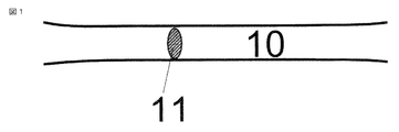
- the aggregate 10 in the particle from the particle emission source end or aggregate 10 to the particle absorption source end in FIG. 1, is provided with a portion having a small vertical cross section 11 in which the particles can move in the direction of particle movement.
- the disturbance of the composition, or the particles having little influence on the S / N ratio due to the heat of the basic element may be emitted from the particle emission source end or absorbed from the particle absorption end, or other aggregates It is possible to release particles to the reaction field or to absorb particles in a uniform state from the particle population.
- atoms / ions / molecular particles can only move in the hole direction.
- the particles can interact with each other from the substances constituting the aggregate and can selectively flow.
- the aggregate of particles in the modifying portion can change the thickness and constituent atoms / molecules, whereby the moving particles can be changed or the flow rate can be adjusted.
- the shape of the quasi-one-dimensional assembly 30 varies depending on the type of particle. A.
- the degree of each thermal noise depends on the disturbance around the cross section of the aggregate and the temperature of the basic element. If the square root of the cross-sectional area S is reduced, even when the temperature of the basic element is room temperature, the transition from the occupied ground state of electrons / holes to the unoccupied state of electrons / holes due to thermal noise does not occur, and When the holes enter the macroscopic quantum state, the SN ratio of the basic element is further improved.
- the atom / ion / molecular particle has a spatial structure having a hole shape, other basic elements are formed between the particles in the particle beam in the aggregate 30, the particles other than the particle beam, the outer wall, and the modification portion.
- the SN ratio of the basic element is improved by the force from the above. C.
- the flow is controlled including laminar flow or turbulent flow.
- energy consumption for maintaining the cooling of the apparatus can be reduced.
- the structure 31 having a protrusion at the particle emission source end or the absorption source end increases the electric field at the end of the particle emission source or near the absorption source end due to the charge at the counter electrode or the target charged particle. This also has the effect of facilitating the release and absorption of particles.
- there is a temperature difference between the particle moving part and the particle emission / absorption source end 1.
- Heat conduction from the particle emission source end to the particle absorption source end other than the thermal energy of the charged particles is suppressed by making the structure other than the assembly 30 vacuum so that heat other than radiation is not easily transmitted. 2.
- a thermoelectric material or thermoelectric conversion element for the aggregate portion 30 where the particle flow or particle beam flow is generated inside the entire absorption / emission basic element, the NEA or PEA effect is enhanced, 3.
- the catalytic effect of a basic element having a particle emission source end or particle absorption source end is enhanced. Collision particles are unlikely to change energy even if their momentum changes due to collision with particles of larger mass.
- low-kinetic energy particles having a good S / N ratio due to the three-dimensional structure of the constituent material, the lattice disturbance, or the heat of the basic element are strongly oozed out to the local nano-order absorption source end 41 using the particles.
- the SN ratio can be reduced with a low kinetic energy particle having a good basic element SN ratio and a larger mass.
- the target particle 45 is improved and a bound target particle energy state having a good S / N ratio is generated.
- charge transfer occurs and a combined target particle flow or particle beam having a good S / N ratio can be produced.
- Aggregates can use holes through which ions are transmitted, holes formed in the membrane, and the like, and can selectively pass particles.
- 52 and 53 indicate that the materials can be different, and the membrane 54 can selectively pass particles.
- Claim 5 is the particle 60 in FIG. 6 where the particle is moved by arranging a portion that generates an electromagnetic field in the vicinity of a spatially narrow place at the modification portion reaching the particle emission source end or the absorption source end 61. It is characterized by controlling the physical and chemical properties. By using an electric field generation source as 62, the voltage-current characteristics of the charged particle flow can be controlled.
- a magnetic field generating source as 62, magnetic atoms are added to the part where the particle flow flows, and by aligning the spins of the magnetic atoms with the magnetic field, the quantum efficiency can be increased by improving the spin polarization rate of the particles. Further, the particle and particle spin diffusion flow due to the concentration gradient field generated when the cross-sectional area of the fine wire obtained by crosslinking the particle emission source and the particle absorption source is about several square nm can be controlled in the same manner. Charged particles or the like adhere to the particle emission source end / particle absorption source end 31 during use or are deformed.
- Possible devices include photocathodes, thermoelectric devices, transistors, diodes, cold cathode tubes, and fuel cells. It is also possible to incorporate these. 7.
- a basic element comprising a combination of the basic elements of claim 6 in series or parallel, or a combination of series and parallel, or a basic element that requires a part other than the part controlling particle flow other than claim 6 or in series or parallel. It is conceivable to use an apparatus composed of a hybrid combination of the above, or a combination of basic elements other than claims 6 to 6 in series or parallel, or a combination of series and parallel.
- modules comprising combinations of these devices and devices and other basic elements are also contemplated in accordance with the scope and spirit of the present invention.
- a system having a low energy particle emission / absorption source with less influence on the S / N ratio than the module according to the claimed invention can be constructed.
- numerous embodiments may be employed to provide methods for implementing devices, modules and systems constructed from basic elements.
- the basic element used here has good energy efficiency because the SN ratio of the basic element is good. Any actuators, modules and systems used to describe this application should not be construed as critical or essential to the invention unless otherwise indicated.
- the influence of the heat of the basic element on the SN ratio can be reduced by reducing the cross-sectional area of the particle emission / absorption source. Since the emission source area is extremely small and a large number of them are arranged close to each other and the emission electron flow can be controlled by a bias current, the energy consumption used for cooling the system is significantly less than that of the hot cathode, and quick control can be performed. Furthermore, by adding magnetic atoms and molecules in the quasi-one-dimensional system, high spin polarization and high quantum efficiency can be obtained with little electron spin depolarization by an external magnetic field.
- Double qubits used in quantum computers are stable charge states in which excess electrons are tunneled between two quantum dots. (Phys. Rev. Lett. 91, 226804-2 (2003)) This control can be performed by applying a drain pulse. Immediate movement can be given by making this high speed.
- Aggregate part of particle absorption and emission basic element Aggregate part of particle absorption and emission basic element. Aggregate part of particle absorption and emission basic element. Basic element for particle absorption and emission. Particle absorption and emission basic element with a separate particle source. Basic element for particle absorption and emission. Particle absorption / release source with control unit.
- Aggregate part which is particle moving part 11 Cross section 20 of aggregate 20 Aggregate part 21 which is particle moving part Particle emission source end 22 Particle absorption source end 30 Aggregate part 31 which is particle moving part Particle emission source end or particle absorption Source end 32 Particle absorption source end or particle emission source end 33 Reaction field 40 close to particle emission / absorption source end Aggregate part 41 as particle movement site Particle emission source end or particle absorption source end 42 Particle absorption source end or particle Release source end 43 Reaction field 44 close to particle emission / absorption source end Target particle emission source 45 Target particle 50 Aggregate parts 51a, 51b and 51c which are particle moving parts Aggregate part 52 which is a particle moving part, 53 Part 54 Aggregate part or boundary between parts 60 Particle movement part 61 Control part
Landscapes
- Physics & Mathematics (AREA)
- Spectroscopy & Molecular Physics (AREA)
- Chemical & Material Sciences (AREA)
- Analytical Chemistry (AREA)
- Engineering & Computer Science (AREA)
- Plasma & Fusion (AREA)
- Physical Or Chemical Processes And Apparatus (AREA)
- Fuel Cell (AREA)
- Electron Sources, Ion Sources (AREA)
- Cold Cathode And The Manufacture (AREA)
Abstract
Description
本発明は、電磁波、電子、ホール、原子・分子等を含む粒子放出・吸収源を持つ基本素子において、他の基本素子と基本素子間の粒子出入、これら粒子同士の相互作用、化学反応等や時間変動する機械・電磁気的力を粒子移動部に許す修飾部が基本素子の放出・吸収端を面して、あるいは1以上の基本素子の放出・吸収端の作る空間内にあり、放出端と吸収端の間にある粒子移動部の構成材料の原子・分子種やその立体構造や格子及びこれらの乱れ、あるいはその装置の熱によるSN比への影響を抑えた低エネルギー粒子を放出・吸収を制御する基本素子とそれら複数の基本素子から構築される装置、モジュール及びシステムに関する。
電磁波や粒子など(以後、粒子を特定しない場合は総称として、粒子と略す)のビームは試料にこのビームを照射することによって試料の物理化学的な構造を解析するために、あるいは物質に照射することによって物理的、化学的に加工を行うために、あるいはエネルギー源とするために利用されている。
物質の構造解明のために走査型電子顕微鏡、透過電子顕微鏡、電子ビーム露光装置、熱電子放出型電子銃、電界放出型電子銃などに電子ビームが用いられる。電界放出型電子銃では電子放出面積が小さくでき、0.4μm半径の陰極先端球面を1800Kに加熱し、電子放出面に印加される電場が~108V/mであると熱電子放出型電子銃に比べ3桁程度高い高輝度電子ビームとなる。しかも熱電子放出型と同様に電界(ショットキー)放出型電子銃は陰極、ショットキーシールド、第一、第二陽極そして陰極の加熱が必要である。また自己収束特性を有する凹面型状のカソードを有するピアス型電子銃構造を用いると電子流は層流として集束する。ピアス型電子銃構造の加熱した陰極より放出される熱電子を、凹面型状の陰極と陽極の間に加速電圧を印加して、電子を陽極孔より引き出すが、凹面型状のカソードは熱電子陰極電子銃のように加熱が必要である。(非特許文献1、非特許文献2)
非特許文献3によると、単層あるいは多層カーボンナノチューブを用いた電界(ショットキー)放出型電子銃では陰極から高さが1.6μmで半径が7.5nm単層カーボンナノチューブの陰極面から陽極間距離が2.13μmで、陰極面から陽極面間に~30V印加されると単層カーボンナノチューブ一本当たり最大~10−7Aの電流となる。
また粒子ビームは物理的、化学的に加工を行うために利用されており、分子線エピタキシー、イオンビームリソグラフィ、イオン注入などがある。収束イオンビームではナノオーダで標的材料を加工することができる。またガスを励起したり、放電を制御したり、プラズマ点火することにも用いられる。
原子や分子の粒子ビームは、粒子の荷電の仕方によってイオンビーム、ラジカルビームなどとよばれる。またビームとして光線などの電磁波を用いたものも考えられる。そのようなものに偏光ビームなどがある。ポジトロンも粒子ビームとなる。特許文献1では、中空の24面体を複数個結合したイコソリッド結合体を利用してポジトロンを発生させていると推証されている。
導体内伝導電子による電気抵抗は温度が下がると格子振動や伝導電子間相互作用による散乱が無視できるようになり通常は不純物散乱が支配する残留抵抗が残る。更に不純物が無い完全結晶でも構成原子の種類や結晶構造によって電気伝導度は大きく変化する。
ランダムなポテンシャル場において二次元以下の導体内伝導電子はアンダーソン局在によると、電気伝導率は系の大きさが大きくなるとゼロとなる(非特許文献4)。以下で述べる伝導する方向に垂直な狭い断面をもつ擬一次元系では三次元なのでアンダソン局在は生じない。
系内の不純物濃度cが増え、系の温度が絶対零度に近づくと、通常は三次元系の伝導電子波動関数が局在するのでその波動関数Ψはexp(−r/ξ(c))と近似できる。ここでrは波動関数の位置変数、ξ(c)はcでの減衰係数である。系のサイズLを動く導体内伝導電子はLがξ(c)よりも小さければ局在することなく電気伝導する。
絶対零度T=0で三次元系伝導電子の状態密度が自由電子の状態密度であるとすると伝導電子の非対角の位置r´=0,r>0での自由電子の2つの異なった波動関数の項とフェルミ分布関数で表される導体の状態密度の積で表される球面波の伝導電子波動相関関数は球面の半径rの−2乗で減衰するが、球面波の伝導電子波動関数が温度によって乱されることはなく、導体を構成する原子種によって伝導電子の状態密度が変わり減衰の仕方は大きく変化する。擬一次元系での伝導電子波動関数も全く同様である。導体内伝導電子の状態密度に依存してるがcが大きくなると擬一次元系での伝導電子波動関数Ψはexp(−χ/ξ(c))と減衰する。ここで伝導する方向の変数をχとしている。擬一次元系での伝導電子波動相関関数はΨと同様に減衰する。
擬一次元系の温度が上昇すると電気抵抗は格子振動や構成原子の違いを反映する電子間相互作用による散乱が効いてきて導体内伝導電子波動相関関数に減衰が生じる。従ってξ(c)は温度Tの関数ξ(c,T)となる(非特許文献5)。その結果、導体内伝導電子による電気抵抗はξ(c,T)、Lそして伝導電子の弾性散乱長leの大小関係で大きく変化する。しかしξ(c,T)には伝導電子間の散乱は伝導電子相関関数を計算する式の状態密度で考慮されているので下記の場合を考えることにする。
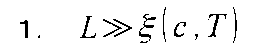
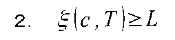
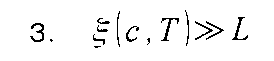

以上のように、導体内伝導電子を含む導体内粒子ビーム以外の導体を構成する原子種や立体構造に依存し、導体温度に依存する減衰や、導体内の不純物濃度に依存した導体内粒子ビームの波動関数の減衰係数をもつ。
電磁波、中性乃至イオン化原子そして電子のビーム発生・吸収素子(以後、本願発明の基本素子と違うことを明記するために素子を用いる)から発生する粒子ビームは粒子ビーム発生・吸収素子の熱による格子振動で粒子ビーム流れが乱されSN比が悪くなる。そのほかにも粒子ビーム流内の荷電粒子のクーロン相互作用や相関相互作用による乱れ、粒子ビーム発生・吸収素子内の不純物、外場による乱れ、粒子ビーム周りの流体によってSN比が悪くなるが、粒子ビーム発生・吸収素子を構成する原子種に依存して粒子ビーム流量は決定される。粒子ビーム発生・吸収素子内の格子振動、不純物や構成原子・分子配列の乱れによって量子力学で計算される粒子ビーム素子内の各粒子エネルギー状態に幅が生じる。粒子ビーム発生・吸収素子の熱雑音は粒子ビーム内のエネルギー準位間遷移を惹き起す。ビーム発生・吸収素子の熱によるSN比への影響は温度によって決まり低温では小さな値となる。
低運動エネルギー粒子として、容易に電子を放出しやすい界面にNEA(Negative Electron Affinity)デバイスがある。これはNEA光電面、二次電子面、冷陰極などとして利用できる。非特許文献6によると、NEA冷陰極の放出面積を極めて小さくし、しかも多数接近して並べて、バイアス電流で放出電子流を制御できるため、加熱した陰極より放出される熱電子を陰極と陽極の間に加速電圧を印加する部位を持つ熱電子陰極電子銃に比べ、エネルギー消費が熱陰極より大幅に少なく即動性のある制御が出来る。しかし安定したNEA表面が必要なためNEAデバイスは放出効率や寿命が問題となる。
光電面は長波長限界があるが、この長波長限界がNEAデバイスはなくなり、熱陰極の場合に必要な負電圧制御電極、加速電極およびビーム制限開孔が必須となるがNEA表面を不要とするために安定なNEA表面が必要なためNEAデバイスは放出効率や寿命が問題となる。高輝度・低エミッタンスのスピン偏極電子源用フォトカソードはNEA表面が必須とするために上記の欠点が問題となる。一方、NEA表面を必要としないピラミッド型のPEA(Positive Electron Affinity)表面のGaAs結晶を用いるスピン偏極電子源用フォトカソードがある。円偏光レーザーをピラミッド型のPEA表面のGaAs結晶に照射し、特定のスピン電子を選択的に荷電子帯から伝導帯へ励起する。この励起した特定のスピン電子集団がPEA表面から放出される前にGaAs結晶内の熱雑音で乱されるが、トンネルによって特定のスピン電子の量子効率やスピン偏極度が高められる。(非特許文献7)
熱電変換は荷電粒子である作業物質が運ぶ熱エネルギーと電荷の伝導体ごとの起電力差を利用して、熱エネルギーと電気エネルギーの変換を行う素子である。排熱から電気エネルギーを得、あるいは電気を流すことで冷却あるいは加熱をすることが可能である。熱電変換の性能指数を改善する熱電変換素子は素子内の熱電材料による起電力を利用し、素子内にある擬一次元部分を利用した荷電粒子の擬一次方向の運動速度分布の熱雑音分布を制御している(特許文献2、特許文献3)。作業物質源は電気回路の導体や半導体である。
粒子源が導体でない例である燃料電池や自動車排気ガス清浄化に代表される環境・エネルギー技術は、エネルギー供給と環境保全を両立する上で、21世紀の人間社会に必要不可欠である。燃料電池に使用する電解質の種類には、アルカリ形、固体高分子形、リン酸形溶融炭酸塩形そして固体酸化物形の五つに分類され、それぞれ特徴、欠点が異なる。携帯用小型電子機器の多機能化に伴いリチウム電池に代わる電源として~数十W程度のマイクロ固体高分子形燃料電池(PEFC)が注目されている。
メタノールの正味のエネルギー密度が非常に高いことを利用するダイレクト・メタノール燃料電池(DMFC)では、メタノール水溶液と酸素ガスを用いるメタノール水溶液に接する膜電極接合体(MEA)において、多量の貴金属アノード触媒を用いてもメタノール酸化速度が遅い。アノードにおけるCO2発生時の生成物は電解質として水酸化カリウム溶液など使用するアルカリ電解質と接触して炭酸塩になることによるアルカリ電解質寿命低下、被毒またアルカリ電解質へのメタノールの浸透の低減等の抵抗過電圧や濃度過電圧や活性化過電圧等の減少の低減が求められている。
室温から100°C以下で作動するPEFCとメタノール燃料電池(MFC)のいづれも高分子電解質膜(PEM)を多孔質支持層+アノード触媒層と多孔質支持層+カソード触媒層から成る二つの電極で挟んだMEAを持つ。このMEAをセパレーターで挟み込んで燃料電池単セルを構成する。MEAにおいて水素ガスと空気中の酸素で作動のPEFCのPEMでは、プロトン伝導性を保つための高分子電解質膜の加湿が必要であるが、このPEMを無・低加湿で動作する高分子電解質への改善、PEMによる水素ガスの遮断性の向上及び空気と接するMEAでの生成水の管理が求められている。
このようにMEAの最も重要な要素材料の1つである触媒層では、目的の反応に対する触媒活性が高く、電気伝導性を持ち、腐食しにくい上に被毒を受けにくいことが求められている。
直径数ナノメートル程度の金属ナノクラスターが酸素を用いた酸化反応を活性化させることが明らかにされて以来、酸素を酸化剤とする酸化反応の触媒が精力的に開発され、直径10nm以下の貴金属ナノ粒子を活性点とする「金属触媒」がある。従来用いられていた金属酸化物のような酸化剤は一般に毒性が高く、よりクリーンな酸化剤が求められ、その点、気体の酸素を酸化剤として用いる酸化反応は副生成物が水のみというクリーンな反応が実現できる。また、高分子に固定化した(内包させた)金触媒を用いたアルコールの酸素酸化反応を起こす触媒が高活性で取り扱いが容易であるのみならず、回収・再使用可能などの利点を有したグリーンな(環境にやさしい)触媒であること。また、二種類の金属を混ぜ合わせることで新たな性質を有する金属種ができる性質を利用し、金と白金から構成されるバイメタルのナノクラスター触媒を高分子に固定化させることにより、より高活性な触媒を合成し、金と白金を組み合わせた場合と、金とパラジウムを組み合わせた場合において、同一のアルコールを原料として用いた場合であっても、前者ではアルデヒドが、後者ではエステルが選択的に得られている(非特許文献8)。
燃料電池に用いられるアノードやカソード触媒層そして金属ナノクラスターを中心に述べたが、一般的に金属ナノクラスターは下記の3種類の特徴を持つことが分子科学研究所の櫻井英博准教授によって報告されている。即ち、
1.金属表面の形状・表面積の変化による反応性の変化:
クラスター状態において量子サイズ効果による電子状態がサイズ・形状によって大きく変化し、それに応じて化学的・物理的性質もサイズ・形状に依存する。
2.触媒活性種の効率的供給源としての金属クラスター:
特にパラジウムクラスター触媒がクロスカップリング反応と称される一連の反応に対して、金属クラスターは多くの場合、活性種を絶えず反応系に供給し、それが触媒サイクル終了後に再びクラスターへ再結合することによって不活性なバルク金属の生成を防ぐメディエイターのような物として働く。触媒活性種はクラスターそのものではなく、クラスターから削り取られること(リーチング)によって生成する裸の単原子状態あるいは数原子状態ではないかと考えられている。また錯体触媒を用いたHeck反応においても、真の活性種はパラジウム錯体そのものではなく、反応系中て分解・生成するクラスターとの報告がある。
3.量子サイズ効果によるクラスター独自の活性:
例えば金クラスターの特徴として表面プラズモン共鳴があるが、クラスターサイズを小さくし、粒径が2nm以下になると、表面プラズモン共鳴は観測されなくなり、もはや金属ではなく分子(molecule)としての性質を帯びると予想されている。室温水溶液中、均一系条件における金クラスターの空気酸化活性は粒径2nm以下になると飛躍的に増大する。これはバルクの金では殆ど触媒活性が無いのと比べ大きな変化である。
一方、代表的な固体酸化物型燃料電池(SOFC)に使用されている酸化物イオン電解質は蛍石型構造が多い。CeO2、ThO2、CaF2、ZrO2、HfO2等は室温から融点までの温度範囲で蛍石型構造を取る。これら酸化物であるホストにゲストであるCaO等のアルカリ土類酸化物、あるいはY2O2等の希土類酸化物は広い範囲で固溶体を造り、種々の格子欠陥が生じても基本的な蛍石型構造が維持されやすいことが知られている(非特許文献9)。
酸化物イオン電解質は蛍石型構造を構成しているホストの一部にゲストの置換混入しても蛍石型構造を維持する仮定下で酸素イオン伝導に関与する蛍石型構造電解質内における空孔子濃度を導く第一近似ヘルムホルツ自由エネルギー、及び空孔子濃度の最近接相互作用依存性の数値解析が行われた。(非特許文献10、非特許文献11)
従来の酸化物イオン導電体と導電機構が異なり、SOFC用の電解質材料として、400~600℃中温域作動が期待されている酸素イオン伝導体がある。その酸化物内のアパタイト型ランタン・シリコン酸化物内の2aサイトに位置するOでc軸方向に列ぶ酸素イオンが酸化物イオン伝導に寄与する。高温電気輸送特性と欠陥化学モデルから、イオン伝導特性に影響を与える逆フレンケル欠陥平衡が検討され、アパタイト型ランタン・シリコン酸化物は理想的な固体電解質であることが明らかになっている。またランタンの一部をネオジウムに置換すると電子伝導の影響が現れ、古典的な欠陥平衡理論のみでは理解できないことが分かった(非特許文献12)。また、ランタンの代わりにネオジウムに置換したNd9.20(SiO4)6O1.8の単結晶の非経験法で線形化された拡張平面波法に局在軌道を拡張した(L)APW+lo法のWIEN2Kによるバンド計算によると非常に小さい電子伝導が生じることを確認している。
燃料電池とは違って、エネルギーを貯える例として蓄電池や電池がある。前者の蓄電池では、いくつかの電解質を挟んで二つの電極は外部負荷の回路と酸化・還元を生じさせる回路が備わっている。
一方、ダイヤモンドはバンドギャップ(5.5eV)が大きいので伝導帯の底が真空準位を超えてしまうNEA状態になり、伝導帯に励起された電子は自由に真空中に飛び出ることができるため、電子放出が置きやすい状態になる。ダイヤモンド表面において水素終端を行うと負の電子親和力(NEA:Negative Electron Affinity)を持ち、酸素終端では正の電子親和力(PEA:Positive Electron Affinity)を持つ。
数1~数3を3次元系に適応した粒子ビームの例として、
・電場を用いて電子やホールを制御するデバイスは電界効果トランジスタ、トランジスタ、ダイオード、コンデンサーなど多く存在する。磁場を用いたものとしてスピン偏極率を制御した素子として特許文献4がある。ここでは格子不整合率5%以下の強磁性層と強誘電層とを接合して電圧によってスピン偏極率を変動させている。
上記のように数1~数3で決まる粒子ビーム状態以外の素子が生じる。この素子に含まれる原子・分子によって素子の物理的性質が大きく変化する。また外界からの擾乱を遮断する外壁で囲まれた素子内の粒子ビーム構成部分は体積変化が起こる系でもある。粒子が移動する構成部分が
A.金属、金属間および準結晶合金、半導体、高速イオン伝導体を含むイオン性物質、金属ガラスおよび酸化物ガラスおよびナノ材料素子内の粒子ビームは
A−1.拡散運動、
A−2.液体乃至気体運動
であり、
B.粒子が移動する構成部分で移動する粒子ビーム以外はない時の素子内の粒子ビームの運動は
B−1.粒子ビームはニュートン運動
をする。
上記A−1の構成部分の体積変化、そこに含まれる原子・分子の濃度変化、温度変化等を考慮する系内の粒子ビーム流量の検討に下記の(数4)を用いて解析されている(非特許文献13)。
中性乃至イオン化原子、熱そして電子の不可逆過程の輸送方程式では、それら中性乃至イオン化原子、熱あるいは電子・・・等から成るn個の全流束に対するi種流束の現象論的な応答で流束Jiとその各々の一般化された熱力学的力χjの間には

印加した温度勾配は熱流と関係する一般化力あるいは化学ポテンシャルの勾配から一般化拡散力を生じさせ、前者に対応する拡散応答である熱流量は熱伝導率で後者は物質流量の拡散係数である。すなわちLijからなるL行列の一部はそれぞれの一般化力とその共役流束とを結びつける対角成分Liiからなる。非対角係数Lijは非共役流束に及ぼす一般化された熱力学的力の影響を決定する。(例:エレクトロマイグレーション、熱電材料)
不可逆過程の特徴はエントロピーの生成である。エントロピー生成速度σを用いるとエネルギー散逸の熱生成速度は
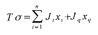

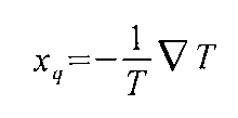
上記A−1とA−2での弾性変形や流動はレオロジー、上記A−2での乱流を含む流体は液体乃至気体論で検討されている。例えば、
・気体乃至液体状態にある中性乃至荷電化原子そして電子から成るビーム流になる場合には、ビーム流に対して乱流状態を含む気体論や流体力学が適用されている。
上記B−1の例としては、
・中性電荷粒子ビームはイオンを加速して中性ガス分子と電荷交換することによって作成される。ナノオーダのデバイス製作では電荷蓄積や真空紫外光などにより欠陥が生成される。またイオンシースによって減速されたり軌道が曲げられたりする。中性電荷粒子ビームはチャージアップしにくく照射対象に損傷を与えにくく、精度の良いデバイスを作成するのに使用されてきている。このためイオン化された粒子を中性電荷粒子と電荷交換させて中性化し中性電荷粒子ビームを作成している。特許文献5ではエネルギーと方向のそろった陽イオン粒子を作製したのち陽イオンと電子の相対速度をほとんどなくすことで効率よく再結合させ、エネルギー分布が単色な中性電荷粒子のビームを得ようとしている。ここでは陽イオンと電子との間の電荷交換散乱断面積や弾性散乱断面積のイオンエネルギーに対する依存性を示し、相対速度が小さいとき電荷交換反応又は結合反応する確率が高くなることを用いている。非特許文献14では負イオンの方が電荷を中性化するのに必要なエネルギーが少ない事を利用して、負イオンとガス分子との電荷交換により中性電荷粒子ビームを作成している。
・低運動エネルギーのビーム内粒子は標的原子・分子などによって散乱され、標的試料表面にしか影響を及ぼさない。これを利用して表面の状態を調べるのに利用されているが粒子によって低運動エネルギーといわれるエネルギーには違いがあり、ISSでは数keV以下で入射方向が標的試料表面と平行に近い、LEEDでは~100eV、プラズマでは~50eV、冷中性子では~5meVとなっている。
本間彰、沢村晃子、山崎初男、中田勝英、谷田弘明、沢村貞史、津守邦彦、線形加速器用低エミッタンス電子銃の設計 北海道大学工学部研究報告第173号(1995)pp.57−63 牧野芳明、飯吉僚、表面電荷法によるショットキー陰極の電界解析 愛知工業大学研究報告書 第41号B(2006)pp.33−40. B.Jean−Marc他 Phys.Rev.Lett.Vol.89(2002)pp.17962−1−19769−4. P.W.Anderson,Phys.Rev.Vol.109(1958)1492 馬淵他、新居浜工業高等専門学校紀要35巻(2002)pp.29−40. テレビジョン学会誌 Vol.32(1978)No.8 p670 M.Kuwahara他 高輝度スピン偏極電子源の開発 第2回日本加速器学会年会・第30回リニアック技術研究会報告集(2005)p.105 S.Kobayashi,et al.,Remarkable Effect of Bimetallic Nanocluster Catalysts for Aerobic Oxidation of Alcohols:Combining Metals Change the Activities and the Reaction Pathways to Aldehydes/Carboxylic Acids or Esters’,Journal of the American Chemical Society,134(2012)16963. T.Kudo and H.Obayashi,J.Electrochem.Soc.123(1976)415. 馬淵眞人、東浦大輔、森田憲治、真鍋純、岡田雄仁:新居浜工業高等専門学校 第42巻(2006)pp.17−23. 尾西康次、森田洋正、東浦大輔、馬淵眞人:新居浜工業高等専門学校 第42巻(2006)pp.25−34. 小林 清:アパタイト型ランタン・シリコン酸化物における逆フレンケル欠陥平衡の解明、科学研究費助成事業(科学研究費補助的)研究成果報告書 平成24年6月22日 H.メーラー 著 固体中の拡散 藤川辰一郎 訳 丸善出版 2007年 J.Plasma Fusion Res.Vol.85,No.4(2009)199
粒子ビームはある試料にあててその物性を調べたり、あるいは物質に照射することで物質の物理化学的性質・形状を変化させたりする。発生粒子の流量を調整できる部位をもつデバイス、トンネル顕微鏡のように吸い込み部位に粒子流の制御を持たせたデバイス、ある粒子放出源端と別の吸収源端と粒子流の制御を持たせて入出力制御するトランジスタ、入射粒子の吸収での二次粒子放出源端あるいはその吸収源端を持つ光電デバイスなどがあり、このような動作の共通部位は多くの分野の素子となっている。素子を通過した粒子ビームのSN比をよくすることで、粒子ビームの粒子ビームの照射対象物あるいは粒子ビーム発生元の物理化学的性質をよりさらに詳しく調べることができる。あるいは粒子ビーム照射試料の照射ダメージを少なくでき、高品質の材料の作製するために極低温にするエネルギーをより少なくできる。また粒子放出源端と吸収源端の粒子の拡散流の制御を持たせて入出力制御するトランジスタの電子と正孔や燃料電池は勿論、中性乃至イオン化原子・分子の入出力制御する触媒作用は従来の触媒に比べ遥かに良い即応性、外部放射線を含む外場雑音に対する耐性さらにトランジスタ等を低温に保って動作させるのに必要なエネルギー消費をより少なくできる。本発明は熱電子線発生装置のような陰極部の過熱、複雑な陰極線の制御によるSN比が悪くなることを生じさせずに低エネルギーの粒子放出あるいは吸収での粒子数、粒子線の方向や粒子運動エネルギー分布を生じさせる素子構成原子・分子や熱による誤差を低め、あるいは量子効率やスピン偏極度が高いといった、SN比への影響を抑えた低エネルギー粒子を放出・吸収を制御する素子(以後、簡単化のために基本素子と略す)とそれら複数基本素子から成るデバイス・モジュール・システムによる構造物を経済的につくることを目的とする。
従来の粒子ビームは粒子ビーム発生熱源を必要とし、粒子放出源までの移動部での粒子がもつ熱の低減がなく粒子発生部や粒子ビーム吸収源の面積が大きいため粒子ビーム制御でのSN比が増加するなどによって粒子ビーム流のSN比が悪くなる。
トランジスタ等の電子デバイスで流れる電子・正孔の放出・吸收源は導体や半導体等、熱電変換素子で流れる作業物質の放出・吸收源は導体、半導体、巨視的量子系等、或いは金属ナノクラスターなどの反応・生成種に伴う放出・吸収源は金属ナノクラスターなどのように、粒子の放出・吸收源は様々ある。粒子ビーム流の途中で粒子ビームの分割或いは粒子ビームへの他の粒子ビームによる混合乃至形状加工乃至化学反応による改変される粒子ビーム流は、外界物質、反応・生成種などの被毒、外部擾乱から守り、上記の分割・混合・形状加工・化学反応による改変そして時間的に変形を許す外壁で保護されている。粒子ビーム流が生じている部分を構成する原子・分子等の集まりを集合体とする。集合体の構造の構造相変化、集合体内転位等の大きな組成、構造、転位等の変化が生じない材料内にある粒子に許されるエネルギー状態はある形状の外壁内の集合体に適用した量子力学で決まる。粒子ビームの粒子をエネルギー準位に分布させ、そのエネルギー準位間隔が広くなれば状態間を変化させにくくなる。(数1~数3参照)更に、粒界拡散高速拡散経路、柱状層多孔構造そしてラメラ構造等或いは、外壁が高分子電解質膜(PEM)や細胞膜等のような外壁形状で構成されることにより、粒子ビームは一方向に制限される。
上記の基本素子の外壁内の粒子ビームは粒子ビームの伝導方向に平行な基本素子の長さL、これに垂直な断面積Sの幾何学的形状であるとする。その外壁には
・個々の粒子ビームに対応する粒子放出・吸収源の部材を持つ。
粒子ビームには中性種があるので、外壁は
・他の粒子ビームへの分割・混合・形状加工・化学反応による改変を許す部位とそれに関する部材を持つ。
・集合体のSを時間変動を含めて変化させるには外壁の形状を変化させる部材を持つ。
・SN比への影響の少ない低エネルギー粒子である上に、集合体のLは上記の修飾部を含む長さである。尚、上記の部材はゼロ個以上である。以後、これらの部材を簡単化のために修飾部と略す。
「技術背景」において、粒子ビーム流の途中で粒子ビームの修飾の例では電子部品の電界効果トランジスタ、トランジスタ等を述べたが、本発明の原理に従った修飾部における粒子ビームの例は1つ以上の実施例を例示し、本明細書とともに、そのような実施例を模式的に説明するものである。これらの概念例では発明の本質を強調した説明になっているが、言うまでもなく発明を特定するものではない。
各集合体の粒子放出・吸收源乃至修飾部での反応場近傍には、必要なら
・反応場と接する粒子放出・吸収源乃至修飾部端表面の導電性コーティング或いはアクチュエータで制御される粒子遮蔽材料部材を
・粒子放出・吸収源乃至修飾部端表面近傍の反応場の反応・生成種の機械的制御する調整板を微調整するアクチュエータを
・全ての反応場近傍に反応・生成物種乃至流の制御する静電・磁場乃至電磁場源を
・粒子放出・吸収源乃至修飾部の酸化、被毒等の汚染を解消させるために外壁に加熱部材を
・反応場から不要な生成種・未反応種を排除するために移送部材を
・各種触媒反応や燃料電池の触媒層での酸化・還元反応では複数の生成種が生じる。これらの複数の生成物種をゼロ以上の粒子ビームにするために個々の粒子ビームに対応する基本素子を
持つ。
上記ゼロ以上の粒子ビームがある基本素子のそれぞれが最短距離で目的の反応種として放出源乃至放出源から反応場に到達し、しかも互いにゼロ以上の粒子ビームが相互作用しない最適な空間配置及び粒子ビーム群のそれぞれのSの空間形状及びLをSN比を最適にする基本素子集団を装置とする。
装置では、
・それぞれの基本素子の外壁にある担持乃至接続部材より装置を組み立てることでこれら基本素子が近傍に纏まるために、装置の外壁は軽量・効率化した担持乃至接続部材を
・カップリング反応、メタセシス反応、チーグラー・ナッタ触媒、トランジスタ、燃料電池、蓄電池、電池等の反応場に対応する装置では、装置にある複数の集合体はゼロ以上のリード線に接続される。外界の外部負荷あるいは電流・電圧源端子に接続するゼロ乃至複数のリード線は、その配線に注意し基本素子、装置、複数の基本素子乃至装置からモジュールが組み立てられる。
そのモジュールの外壁には
・基本素子から装置の構築された際の装置の外壁が軽量・効率化されたのと同様な軽量・効率化された担持乃至接続部材を
・複数のモジュールの各々がゼロ以上の外界の外部負荷あるいは電流・電圧源端子に接続する複数のリード線を持つ高位モジュール、更なる高位モジュール・・・となってシステムに組み立てられようにそれぞれのモジュール外壁に、基本素子から装置の構築された際の装置の外壁が軽量・効率化されたのと同様な軽量・効率化された担持乃至接続部材を
持つ。上記のモジュール外壁の担持乃至接続部材は基本素子、装置そしてモジュールに対して共通であることが望ましい。
「技術背景」においては、触媒反応系、電子部品の電界効果トランジスタ、トランジスタ等や熱電変換素子や燃料電池・蓄電池や電子銃等を述べたが、これらに対応する装置、モジュールは本発明の原理に従った1つ以上の実施例を例示し、本明細書とともに、そのような実施例を模式的に説明するものである。発明の概念例では発明の本質を強調した説明になっているが、言うまでもなく発明を特定するものではない。
上記のような外壁と集合体が基本素子であり、外壁内で制限された集合体内の粒子ビーム流制御の設計は次のような分類になる。
a.質量の軽い電子、正孔等では、外壁が粒子ビーム流方向に垂直断面積が狭くなる外壁形状のとき、粒子の存在できるその外壁形状におけるエネルギー準位間隔が熱エネルギーより広くなると粒子は熱エネルギーによる状態間遷移を起こしにくくなる。その結果、粒子移動は擬一次元的になり散乱されにくくなる。
b.電子、正孔等より質量の重い粒子では、ある外壁形状内で集合体中の粒子ビーム流方向に垂直方向の粒子運動が小さくなれば粒子移動は擬一方向的になり、しかも粒子ビーム流を最大にする。
c.ナノ材料中の拡散のような高速拡散経路、柱状層多孔構造やラメラ構造等の外壁あるいは高分子電解質膜(PEM)や細胞膜等のような外壁形状の内部の粒子ビームと粒子ビーム以外で基本素子の放熱にも関与する粒子が乱流を含む気体・液体状態であるとき、粒子移動を擬一方向で、しかも粒子ビーム流を最大にする。
d.電子銃のように粒子ビーム以外の原子・分子等を排除して、粒子ビーム流方向に垂直方向の運動エネルギー分布の広がりが熱エネルギーより非常に小さくした粒子ビーム流を最大にする。
集合体が上記a~dであると下記のような設計が可能である。
a.ナノサイズ以上の基本素子の全体内部で粒子ビーム流が生じている集合体が結晶構造の部材とする。不純物を含み粒子ビームと外界とを隔てる保護外壁等の側面界面原子・分子や結晶構造の配列の乱れ、集合体内の熱運動によって許されるエネルギー準位が複雑に幅をもつ。熱運動による擾乱のみの集合体では運動の方向に垂直な断面の周囲に構成原子・分子配列に乱れがあってもその断面空間内にある粒子流の許されるエネルギー状態は量子力学で完全に決まる。擬一次元なバリスティック伝導方向に基本素子の長さL、そしてそれに垂直な断面積Sの大きさである集合体の最低エネルギー準位は断面中心部での存在確率が大きく断面の周囲での構成原子・分子による乱れの影響が少ないSを決める。LとSの大きさを持つ集合体の次のエネルギー準位に至るまでの粒子のエネルギーが基本素子の熱エネルギーに比べて大きいときには、Sの平方根がナノオーダ程度でない場合と比べるとSN比のよい粒子のエネルギー状態になる。集合体内部の粒子移動部では格子振動や粒子等と相互作用しながら拡散伝導をするが断面積が狭くなると擬一次元的な運動となる。断面積が狭くなり断面に垂直に移動する粒子の減衰係数より一桁以上距離が短くなると擬一次元なバリスティック伝導となりうる。バリスティック伝導では集合体の周囲での構成原子・分子などの不純物散乱が無視できSN比がより改善する。
従って、不純物濃度cを集合体内部に持ち、水素、電子そして正孔などの擬一次元なバリスティック伝導に最適なナノオーダー以上の集合体の設計は
a−1.集合体の幾何学的な形状をある形状に決定する。
a−2.集合体を構成する原子・分子や空孔を含む不純物原子・分子の種類とそれらの混成割合を決め、そし

a−3.配列が決定された集合体に量子力学を適用し、LとSの変数としてエネルギー状態を決定する。
a−4.熱による伝導粒子のエネルギー状態への分布と状態密度とに依存してるが、空孔を含む不純物原子・分子の配置に依存するcの関数として擬一次元系での伝導粒子波動関数Ψは
exp(−χ/ξ(c,T))と減衰係数ξ(c,T)で減衰する。ここで伝導する方向の変数をχとしている。擬一次元系での伝導粒子の二次以上の波動相関関数も熱による伝導粒子のエネルギー状態への分布と状

a−6.上記a−2.での基本素子の種類と混成割合や集合体内の配列少しづつ変化させて、上記A−3.~A−5.を行い、最適なナノオーダー以上の集合体を構成する原子・分子や空孔を含む不純物原子・分子の種類の最適化を行う。
a−7.上記a−1.で決めた初期の形状から粒子が荷電乃至磁荷粒子であれば修飾部にある時空変動する電磁場による影響を含め、Lと擬一次元系の場所に依存して変化するSのみならず、集合体の形状を変化させてSN比への影響を抑える最適化をする。
上記bでは、Lに沿った方向をx軸方向とし、時間t+τでx軸値がχでLに垂直面内に存在する時間変動する拡散粒子の濃度Cd(χ,t+τ)のtでχ−XでのCd(χ−X,t)に対する均衡から拡散方程式乃至マスター方程式を導く、時間依存する拡散粒子の濃度Cd(χ,t)による擬一方向の準バリスティック伝導するが他の粒子は熱振動以上の変位をするが気体乃至液体状態にならない粒子から成る集合体に最適なナノオーダー以上の集合体の設計は、
b−1.集合体を構成する準バリスティック伝導をしない粒子である原子・分子や空孔を含む不純物原子・分子の種類とそれらの混成割合を決定する。
ここで、




b−4.Cd(χ,t)が変化する速度は、X=0でτ=0近傍でのCd(χ,t+τ)と
Cd(χ−X,t)の展開によって、

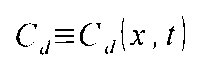
b−5.上式11の右辺2項目はi種流束の現象論的な応答では流束Jiを生じさせその各々の一般化された熱力学的力χjには数4の関係があり、擬一方向な準バリスティック伝導する粒子以外の粒子影響を伝導する粒子に与える変動の効果は〈X2〉aveとなるので、擬一方向な準バリスティック伝導する粒子の拡散係数と関係する。
b−6.上式11の右辺3項目以上の擬一方向な準バリスティック伝導する粒子以外の粒子影響を、伝導する粒子に与える変動の効果は〈X3〉ave、〈X4〉ave・・・となり、擬一方向な準バリスティック伝導する粒子のガウス分布からのズレを表す。
b−7.上記b−1.で決めた初期の形状から、粒子が荷電乃至磁荷粒子であれば修飾部にある時空変動する電磁場による影響を含め、Lと擬一方向系の場所乃至時間に依存して変化するSのみならず、集合体の形状を変化させて最適化する。
上記cでは、
c−a.高速拡散経路等の形状がLとSの基本素子では、外壁で制限されたLに垂直断面Sに穴形状の高速拡散経路Lに沿って擬一方向に粒子ビームは伝導するが、他の粒子は熱振動で気体乃至液体状態になっている集合体である。
c−b.LとSが柱状層多孔構造、ラメラ構造等がLを揃えて内在する基本素子では、上記c−a.のSに垂直に柱状層多孔やラメラ構造等の柱、隔壁等が配置し、Lに沿って粒子ビームは擬一方向に伝導するが他の粒子は熱振動で気体乃至液体状態になっている集合体である。
c−c.LとSのPEMや細胞膜等を持つ基本素子では、基本素子の膜形状を維持する部材、擬一方向に伝導しやすくする形状の部材等によって、Lに沿って擬一方向に粒子ビームは伝導するが他の粒子は熱振動で気体乃至液体状態になっている集合体である。
上記c−a.~c−c.の基本素子内では、粒子ビームに相当する粒子或いは粒子から成る微粒子或いは他の原子・分子と化学結合した分子による濃度Cdは数12で決まる。しかもSでLに沿った擬一方向にSN比への影響を抑える粒子ビームはSでLの境界条件を考慮して数11を解くことになる。
それぞれの集合体内のL方向で、SN比への影響を抑える粒子ビームが擬一方向に最大に伝導する設定エネルギーEの粒子ビームの集団内粒子の条件、そして最適なナノオーダー以上の集合体の設計は、
c−1.上記c−a.~c−c.の外壁、柱、隔壁、部材等による粒子ビーム散乱、粒子ビーム以外の集合体粒子との散乱や干渉、粒子ビームの粒子同士に散乱や干渉で目標とする擬一方向軌道からそれぞれずれを求める。
c−2.粒子ビームの集団内粒子の目標とする擬一方向軌道上の設定エネルギーEからのエネルギー広がり〈ΔE〉=〈ΔE⊥〉+〈ΔE‖〉とEとの比である〈ΔE〉/Eを弾性変形や流動はレオロジーで、乱流状態を含む気・液相は気体論・液体論を用いて求める。ここで、〈ΔE‖〉は粒子移動の一次元方向の、〈ΔE⊥〉は一次元方向に垂直方向の運動によるエネルギー広がりを持つ。ここで、〈A〉は物理量Aの集合体内の外壁に影響された粒子に対する平均である。
c−3.Eが小さいと、〈ΔE‖〉/Eや〈ΔE⊥〉/Eが大きくなるため、粒子が荷電乃至磁荷粒子であれば修飾部にある時空変動する電磁場による影響を含め、集合体内で粒子ビーム以外の粒子のLと擬一方向系の場所乃至時間に依存して変化するSのみならず、集合体の形状を変化させてSN比への影響を抑える最適化をする。
上記d.では、数11で表される濃度Cdのみ存在する。集合体に最適なナノオーダー以上のLと場所乃至時間に依存して変化するSの集合体の設計は、
d−.1.設定エネルギーEの粒子ビームの集団内粒子間と粒子と外壁間の相互作用、
d−2.粒子が荷電乃至磁荷粒子であれば修飾部にある時空変動するSや電磁場によって平衡軌道を中心に振動をする。
d−3.上記cと同様に、粒子ビームの集団内粒子振動によるエネルギー広がり〈ΔE〉=〈ΔE⊥〉+〈ΔE‖〉とEとの比〈ΔE〉/Eを巨視的量子系を含む量子論、古典論、熱力・統計力学等を用い求める。
d−4.上記cと同様に、Eが小さいと、〈ΔE‖〉/Eや〈ΔE⊥〉/Eが大きくなる。ここでの〈A〉は物理量Aの集合体内である外壁に影響された粒子ビームに対する平均である。
d−5.〈ΔE‖〉/Eや〈ΔE⊥〉/Eを集合体内の荷電・磁乃至中性粒子の分布や集合体形状の時空変動を含めて変化させてSN比への影響を抑える最適化をする。
一般には、集合体は上記のa~cで綺麗に分類できない。また、a~cとdを含めて計算機シミュレーションの発展と伴に、上記の集合体に最適なナノオーダー以上の集合体の設計は一例であって特定されるものではない。
請求項1は図1における粒子放出源端乃至集合体10から粒子吸収源端までにある粒子において、粒子の移動方向に粒子が移動可能な垂直な断面11が小さい部分を集合体10に備えることによって、構成材料の立体構造の格子又は組成の乱れ、あるい基本素子の熱によるSN比への影響の少ない粒子を粒子放出源端から放出又は粒子吸収端から吸収すること、あるいは他の集合体や反応場に放出、あるいは粒子集団から状態のそろった粒子を吸収することを可能とする。
本発明の原理に従ったSN比への影響を低減する基本素子の図示で、外壁、粒子放出・吸収源、修飾部、外壁内部にある部材、他の基本素子や他の部材との担持乃至接続部材、反応場等を除いて、基本素子を集合体だけに注目する添付の図面は、本明細書の一部を構成する1つ以上の実施例を図示し、本明細書とともに、そのような実施例を簡略・明瞭で模式的に説明するものである。以下の発明の概念図も発明の本質を強調した説明になっているが、言うまでもなく発明を特定するものではない。
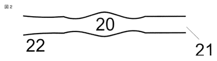
またアパタイト型ランタン・シリコン酸化物あるいは高速拡散経路、柱状層多孔構造のように、穴形状をもつ空間構造からなる集合体では原子・イオン・分子粒子は穴方向の運動だけが可能となる。粒子が集合体を構成する物質から相互作用を受け選択的な流れが可能である。図2のように、修飾部で粒子の集合体は太さや構成する原子・分子を変えることが可能であり、それによって移動する粒子を変化させ、あるいは流量を調整することが可能である。
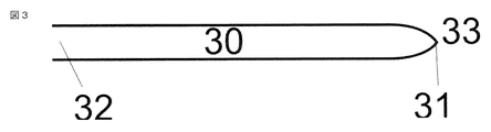
擬一次元的な集合体30の形状は粒子の種類によって異なる。上記a.で記載のように、電子・正孔では、それぞれの熱雑音の程度は集合体の断面周りの乱れと基本素子の温度に依存する。その断面積Sの平方根が小さくなれば基本素子の温度が室温でも熱雑音による電子・正孔の占有基底状態からの電子・正孔の非占有状態への状態間遷移が生じなくなり、しかも電子乃至正孔が巨視的量子状態になると、更に基本素子のSN比が改善される。上記b.で記載のように、原子・イオン・分子粒子では穴形状を持つ空間構造からなる場合、集合体30にある粒子ビーム内の粒子間、粒子ビーム以外の粒子、外壁、修飾部を通して他の基本素子等からの力により基本素子のSN比が改善される。上記c.で記載のように、穴形状の径が大きいときは流れは層流あるいは乱流ということも含め制御される。その結果、装置の冷却維持のエネルギー消費を削減できる。粒子が荷電粒子の場合、粒子放出源端あるいは吸収源端に突起のある構造31とすることで対極部の電荷あるいは標的荷電粒子による粒子放出源端あるいは吸収源端近傍での電界が強くなることにより粒子が放出・吸収されやすくするという効果も持つ。粒子移動部と粒子放出・吸収源端で温度差があるとき、
1.集合体30以外の部分を真空にするなどで輻射以外の熱が伝わりにくい構造にすることで荷電粒子がもつ熱エネルギー以外は粒子放出源端から粒子吸収源端までの熱伝導が抑え、
2.吸収・放出基本素子の全体内部で粒子流乃至粒子ビーム流が生じている集合体部分30に熱電材料あるいは熱電変換素子を用いて、NEA乃至PEA効果を高め、
3.粒子放出源端乃至粒子吸収源端を持つ基本素子の触媒効果などを高める。
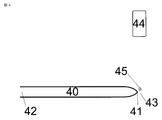
衝突粒子はそれより大きな質量の粒子との衝突によってその粒子の運動量は変えてもエネルギーを変えにくい。請求項2は構成材料の立体構造や格子の乱れ、あるいは基本素子の熱によるSN比のよい低運動エネルギーの粒子を、その粒子を利用する局所的でナノオーダの吸収源端41に強く染みださせることによって、その場所で被標的粒子の放出源44から放出された被標的粒子45と相互作用させることによって、基本素子のSN比がよい低運動エネルギー粒子とそれより大きい質量でSN比の低減が改善し、被標的粒子45が結合してSN比がよい結合被標的粒子エネルギー状態が生じる。あるいは電荷の移動が起こり、SN比の良い結合被標的粒子流れ乃至粒子ビームを造ることができる。基本素子のSN比がよい低運動エネルギー粒子として電子を用いることで、SN比のよい質量の大きな低エネルギー荷電粒子の電荷を打ち消し、低運動エネルギーではSN比のよい中性電荷低エネルギー被標的粒子を得ることを可能とする。一方、高エネルギー状態では熱エネルギーは無視できるので常にSN比はよい。
粒子として、原子、イオン乃至分子を使うことによって、移動開始前あるいは移動開始後に、電子、ホール、原子、イオン、分子と反応を起こさせることができる。請求項3はこの時集合体を通過する粒子を制御することで反応を制御することを可能とする。複数の基本素子が空間配置を取る装置の図5において、図5の各基本素子の集合体を移動する粒子は集合体50と集合体51で種類を変化させることも可能である。集合体はイオンが伝わる穴や膜に空いた穴などを利用することができ、選択的に粒子を通過させることも可能である。52と53は材質が違いうることを示しており、膜54は選択的に粒子を通過させうるものである。
上記の装置は高分子電解質膜(PEM)の多孔質支持層+アノード触媒層にも適用できるが、上記の図5に関する説明においては、請求項に係る発明の様々な態様の完全な理解を提供するため、例えば粒子放出・吸収源端表面の形状変形、反応場の変形および温度変化、反応場に作用する電磁場強度変化、反応場と接する粒子放出・吸収源端表面のコーティング或いは材料、反応場の反応・生成物の機械的制御する板のアクチュエータ、基本素子・モジュール・装置から成る混合構築物と外部負荷を考えたシステム等、及び基本素子、装置、上位のモジュールを含めたモジュールそしてシステムには放熱、保護等の最適化が説明されなければならない。しかしながら、そのような特定は個々の系の説明のために提示されるものであり、以下の請求項も含めて請求項に係る発明に関する限定として解釈されるべきではない。
基本素子を組み合わせることによって機能を修飾あるいは別の機能を持たせることを請求項4は可能とする。ある基本素子と別の基本素子の集合体は1対1で対応させる必要はなく、ある1つの基本素子の集合体に対して別の複数個の基本素子の集合体が対応させることも可能である。また、集合体毎に移動する粒子の種類が変わりうるので基本素子の集合体が別の基本素子の集合体と対応していなくてもいい。
請求項5は、図6の粒子が移動する部位60において、粒子放出源端あるいは吸収源端61に至る修飾部で空間的に狭い場所の近傍62に電磁場を発生する部位を配すことにより粒子の物理・化学的特性を制御することを特徴とする。62として電場発生源を用いることによって荷電粒子流の電圧電流特性を制御できる。62として磁場発生源を用いることにより粒子流が流れる部分に磁性原子を添加し、この磁性原子のスピンを磁場で揃えることにより粒子が持つスピンの偏極率の向上によって量子効率を大きくできる。また粒子放出源と粒子吸収源とを架橋した細線の断面積が数平方nm程度で生じる濃度勾配場による粒子や粒子スピン拡散流も同様に制御できる。
粒子放出源端・粒子吸収源端31には使っているうちに荷電粒子等が付着したり変形をしたりする。近傍33に熱を加えられる部位を配すことにより粒子放出・吸収源端31の使用による吸着原子・分子による汚れや変形を少なくすることを可能とする。
請求項6はSN比がよい粒子放出源、粒子吸収源があるときは粒子流を制御する部位以外は必要な部位はなく、即応性の良い、SN比が従来に比べ改善する装置が可能となる。また装置の冷却に対するエネルギー消費を低く抑えることよって、装置の直・並列あるいは複合配列を組み込んだモジュールが外界との接続において効率をよくすることが可能となるシステムができる。装置として光電面、熱電装置・トランジスタ・ダイオード・冷陰管・燃料電池などが考えられる。またこれらを組み込むことが考えられる。
請求項6の基本素子の直列あるいは並列、または直列と並列の混成した組み合わせから成る、或いは請求項6以外で粒子流を制御する部位以外を必要とする基本素子の直列あるいは並列、または直列と並列の混成した組み合わせから成る、或いは請求項6乃至請求項6以外の基本素子が直列あるいは並列、または直列と並列の混成した組み合わせから成る装置が考えられる。明らかなように、これらの装置と装置や他の基本素子からなる組み合わせからなるモジュールも本発明の範囲及び精神に従って意図される。このために請求項に係る発明に従ったモジュールよりSN比への影響の少ない低エネルギー粒子放出・吸収源を持つシステムが構築できる。明らかなように、基本素子から構築される装置、モジュール及びシステムを実現する方法を提供することには、数多くの実施形態が採用され得る。
請求項7は粒子溜めに基本素子を用いることにより粒子溜めに粒子を吸収させてエネルギーを貯蔵し、あるいは粒子溜めから基本素子を用いて粒子を放出させ粒子のエネルギーを利用する事を可能とする。ここで用いられる基本素子では基本素子のSN比がいいのでエネルギー効率がよい。
本出願の説明に使用された如何なるアクチュエータ、モジュールそしてシステム、特に断らない限り、本発明に決定的に重要な、あるいは不可欠なものとして解されるべきではない。
11 集合体の断面
20 粒子移動部位である集合体部
21 粒子放出源端
22 粒子吸収源端
30 粒子移動部位である集合体部
31 粒子放出源端または粒子吸収源端
32 粒子吸収源端または粒子放出源端
33 粒子放出・吸収源端に近接する反応場
40 粒子移動部位である集合体部
41 粒子放出源端または粒子吸収源端
42 粒子吸収源端または粒子放出源端
43 粒子放出・吸収源端に近接する反応場
44 被標的粒子の放出源
45 被標的粒子
50 粒子移動部位である集合体部
51a、51b、51c 粒子移動部位である集合体部
52、53 部位
54 集合体部または部位間の境界
60 粒子移動部位
61 制御部
Claims (7)
- 粒子流方向の運動に略垂直方向での許容される準位間エネルギーが素子の熱エネルギーに比べ大きくなるぐらいその粒子移動可能断面積が小さく、粒子発生部位乃至粒子移動部位から粒子放出端まであるいは粒子消滅部位乃至粒子移動部位から粒子吸収端まで(以後、素子と略す)の距離があることにより、立体構造や格子、組成の乱れ乃至素子の熱によるSN比への影響を抑え、そのSN比への影響が粒子の利用部位にほとんどそのまま伝わることを特徴とする粒子放出源乃至粒子吸収源を持つ基本素子。
- 請求項1に記載の粒子放出源において発生した低運動エネルギーでSN比がよい荷電粒子により、低運動エネルギーに制御された荷電粒子を中性化することにより中性化された粒子の熱によるSN比への影響が小さいことを特徴とする中性粒子発生源素子。
- 請求項1に記載の粒子放出乃源において発生したSN比がよい粒子を反応に用いることにより、あるいは、粒子吸収源においてSN比のよい粒子を吸収することによって、運動方向やエネルギー値の揃った生成物、熱乃至電気を得ることを特徴とする基本素子。
- 請求項1、請求項2、請求項3の基本素子を組み合わせることによって、必要なら移動する粒子の種類を動的或は静的に変化させ、或は基本素子の機能を高め、或は修飾することを可能とすることを特徴とする装置。
- 請求項1、請求項2、請求項3、請求項4に記載のSN比を改善する粒子放出源乃至粒子吸収部位において発生端に至る部位に放出粒子の自由度を制御し発生粒子乃至吸収粒子の流量を調整できる、あるいは必要ならば熱を加えられる部位を持つことを特徴とする粒子放出源乃至粒子吸収素子。
- 請求項1、請求項2、請求項3、請求項4に記載の素子を直・並列あるいは混生配列できることを特徴とする装置。
- 請求項1、請求項4、請求項5に記載の粒子放出源乃至粒子吸収部位として粒子溜めを用い、その外的条件を制御することによって少なくとも2個の粒子溜め間で粒子を移動させることによって、エネルギーを貯蔵・放出することを特徴とする、及び請求項1、請求項4、請求項5、請求項6記載の装置から成るシステム。
Priority Applications (6)
| Application Number | Priority Date | Filing Date | Title |
|---|---|---|---|
| RU2016140537A RU2696344C2 (ru) | 2014-03-17 | 2014-03-17 | Элементарный элемент |
| CN201480078944.9A CN106458577A (zh) | 2014-03-17 | 2014-03-17 | 基本元件 |
| JP2016508439A JPWO2015141015A1 (ja) | 2014-03-17 | 2014-03-17 | 基本素子 |
| EP14886203.0A EP3121146A4 (en) | 2014-03-17 | 2014-03-17 | Elementary element |
| US15/125,166 US20170231079A1 (en) | 2014-03-17 | 2014-03-17 | Elementary element |
| PCT/JP2014/059380 WO2015141015A1 (ja) | 2014-03-17 | 2014-03-17 | 基本素子 |
Applications Claiming Priority (1)
| Application Number | Priority Date | Filing Date | Title |
|---|---|---|---|
| PCT/JP2014/059380 WO2015141015A1 (ja) | 2014-03-17 | 2014-03-17 | 基本素子 |
Publications (2)
| Publication Number | Publication Date |
|---|---|
| WO2015141015A1 WO2015141015A1 (ja) | 2015-09-24 |
| WO2015141015A9 true WO2015141015A9 (ja) | 2016-11-24 |
Family
ID=54144015
Family Applications (1)
| Application Number | Title | Priority Date | Filing Date |
|---|---|---|---|
| PCT/JP2014/059380 Ceased WO2015141015A1 (ja) | 2014-03-17 | 2014-03-17 | 基本素子 |
Country Status (6)
| Country | Link |
|---|---|
| US (1) | US20170231079A1 (ja) |
| EP (1) | EP3121146A4 (ja) |
| JP (1) | JPWO2015141015A1 (ja) |
| CN (1) | CN106458577A (ja) |
| RU (1) | RU2696344C2 (ja) |
| WO (1) | WO2015141015A1 (ja) |
Families Citing this family (3)
| Publication number | Priority date | Publication date | Assignee | Title |
|---|---|---|---|---|
| EP3477390A1 (en) * | 2017-10-25 | 2019-05-01 | ASML Netherlands B.V. | Inspection tool, lithographic apparatus, electron beam source and an inspection method |
| CN113952894B (zh) * | 2020-07-21 | 2025-02-14 | 李辉雄 | 减容或有机物分解反应装置 |
| CN114927396B (zh) * | 2022-04-24 | 2023-05-12 | 电子科技大学 | 一种实时控制NEA GaN电子源扩散长度的方法 |
Family Cites Families (5)
| Publication number | Priority date | Publication date | Assignee | Title |
|---|---|---|---|---|
| JP4069624B2 (ja) * | 2000-03-31 | 2008-04-02 | 株式会社日立製作所 | 走査電子顕微鏡 |
| JP4751635B2 (ja) * | 2005-04-13 | 2011-08-17 | 株式会社日立ハイテクノロジーズ | 磁界重畳型電子銃 |
| JP2007149659A (ja) * | 2005-10-27 | 2007-06-14 | Sumitomo Electric Ind Ltd | 電界放出型電子銃、電子顕微鏡、及び電子ビーム露光機 |
| WO2012086419A1 (ja) * | 2010-12-22 | 2012-06-28 | 株式会社日立ハイテクノロジーズ | 荷電粒子放出銃及び荷電粒子線装置 |
| JP2014046451A (ja) * | 2012-09-02 | 2014-03-17 | Masato Mabuchi | 熱によるsn比への影響の少ない低エネルギー粒子放出装置乃至粒子吸収装置 |
-
2014
- 2014-03-17 EP EP14886203.0A patent/EP3121146A4/en not_active Ceased
- 2014-03-17 JP JP2016508439A patent/JPWO2015141015A1/ja active Pending
- 2014-03-17 US US15/125,166 patent/US20170231079A1/en not_active Abandoned
- 2014-03-17 CN CN201480078944.9A patent/CN106458577A/zh active Pending
- 2014-03-17 RU RU2016140537A patent/RU2696344C2/ru active
- 2014-03-17 WO PCT/JP2014/059380 patent/WO2015141015A1/ja not_active Ceased
Also Published As
| Publication number | Publication date |
|---|---|
| RU2016140537A (ru) | 2018-04-18 |
| WO2015141015A1 (ja) | 2015-09-24 |
| EP3121146A1 (en) | 2017-01-25 |
| JPWO2015141015A1 (ja) | 2017-04-13 |
| RU2696344C2 (ru) | 2019-08-01 |
| CN106458577A (zh) | 2017-02-22 |
| US20170231079A1 (en) | 2017-08-10 |
| EP3121146A4 (en) | 2018-04-25 |
Similar Documents
| Publication | Publication Date | Title |
|---|---|---|
| Zhang et al. | Metal single‐atoms toward electromagnetic wave‐absorbing materials: insights and perspective | |
| Yang et al. | The role of geometric sites in 2D materials for energy storage | |
| Huang et al. | Recent progress in the application of ion beam technology in the modification and fabrication of nanostructured energy materials | |
| Wang et al. | Tuning oxygen reduction reaction activity via controllable dealloying: a model study of ordered Cu3Pt/C intermetallic nanocatalysts | |
| Xiao et al. | Hierarchically porous graphene as a lithium–air battery electrode | |
| Rahman et al. | Semiconductor thermionics for next generation solar cells: photon enhanced or pure thermionic? | |
| Yang et al. | A stable, magnetic, and metallic Li3O4 compound as a discharge product in a Li–air battery | |
| Safari et al. | Kinetics of oxygen reduction in aprotic Li–O2 cells: a model-based study | |
| Schindler et al. | Surface photovoltage-induced ultralow work function material for thermionic energy converters | |
| Diao et al. | Photon-enhanced thermionic emission solar energy converters with GaAs wire array cathode under external electric field | |
| Chung et al. | Understanding a degradation mechanism of direct methanol fuel cell using TOF-SIMS and XPS | |
| Nojeh | Carbon nanotube electron sources: from electron beams to energy conversion and optophononics | |
| Ashok et al. | Plasma‐Induced Nanocrystalline Domain Engineering and Surface Passivation in Mesoporous Chalcogenide Semiconductor Thin Films | |
| Yang et al. | First principles studies of nitrogen doped carbon nanotubes for dioxygen reduction | |
| Li et al. | Machine-learning-accelerated screening of single metal atoms anchored on MnPS 3 monolayers as promising bifunctional oxygen electrocatalysts | |
| WO2015141015A9 (ja) | 基本素子 | |
| Diao et al. | Comparative study of negative electron affinity GaAs nanowire photocathodes with Cs/O and with Cs/NF3 from first‐principles | |
| Li | Stationary Direct Methanol Fuel Cells Using Pure Methanol | |
| Zhao et al. | Access to ultrafast surface and interface carrier dynamics simultaneously in space and time | |
| Lu et al. | Ultrahigh lithium storage capacity of Al2C monolayer in a restricted multilayered growth mechanism | |
| Chae et al. | Tunable Onset of Hydrogen Evolution in Graphene with Hot Electrons | |
| Ashraf et al. | Aligned Bilayer of Single-Walled Carbon Nanotubes Suppresses the Polysulfide Shuttle in Li–S Batteries | |
| Dhobi et al. | Scattering of free electrons with hydrogen atoms in proton exchange membrane fuel cell system | |
| Song et al. | An Ultra‐Low Discharge and High Energy Efficiency Li‐CO2 Battery Enabled by Plasmon‐Enhanced AuRu‐TiO2 Bifunctional Cathode | |
| JP2010272383A (ja) | 燃料電池電極及びその製造方法 |
Legal Events
| Date | Code | Title | Description |
|---|---|---|---|
| 121 | Ep: the epo has been informed by wipo that ep was designated in this application |
Ref document number: 14886203 Country of ref document: EP Kind code of ref document: A1 |
|
| ENP | Entry into the national phase |
Ref document number: 2016508439 Country of ref document: JP Kind code of ref document: A |
|
| NENP | Non-entry into the national phase |
Ref country code: DE |
|
| REEP | Request for entry into the european phase |
Ref document number: 2014886203 Country of ref document: EP |
|
| WWE | Wipo information: entry into national phase |
Ref document number: 2014886203 Country of ref document: EP |
|
| ENP | Entry into the national phase |
Ref document number: 2016140537 Country of ref document: RU Kind code of ref document: A |