WO2015141737A1 - 電子機器 - Google Patents
電子機器 Download PDFInfo
- Publication number
- WO2015141737A1 WO2015141737A1 PCT/JP2015/058099 JP2015058099W WO2015141737A1 WO 2015141737 A1 WO2015141737 A1 WO 2015141737A1 JP 2015058099 W JP2015058099 W JP 2015058099W WO 2015141737 A1 WO2015141737 A1 WO 2015141737A1
- Authority
- WO
- WIPO (PCT)
- Prior art keywords
- semiconductor integrated
- integrated circuit
- cooling element
- radiation
- radiation detection
- Prior art date
- Legal status (The legal status is an assumption and is not a legal conclusion. Google has not performed a legal analysis and makes no representation as to the accuracy of the status listed.)
- Ceased
Links
Images

Classifications
-
- H—ELECTRICITY
- H10—SEMICONDUCTOR DEVICES; ELECTRIC SOLID-STATE DEVICES NOT OTHERWISE PROVIDED FOR
- H10W—GENERIC PACKAGES, INTERCONNECTIONS, CONNECTORS OR OTHER CONSTRUCTIONAL DETAILS OF DEVICES COVERED BY CLASS H10
- H10W40/00—Arrangements for thermal protection or thermal control
- H10W40/20—Arrangements for cooling
- H10W40/22—Arrangements for cooling characterised by their shape, e.g. having conical or cylindrical projections
-
- B—PERFORMING OPERATIONS; TRANSPORTING
- B64—AIRCRAFT; AVIATION; COSMONAUTICS
- B64G—COSMONAUTICS; VEHICLES OR EQUIPMENT THEREFOR
- B64G1/00—Cosmonautic vehicles
- B64G1/10—Artificial satellites; Systems of such satellites; Interplanetary vehicles
-
- B—PERFORMING OPERATIONS; TRANSPORTING
- B64—AIRCRAFT; AVIATION; COSMONAUTICS
- B64G—COSMONAUTICS; VEHICLES OR EQUIPMENT THEREFOR
- B64G1/00—Cosmonautic vehicles
- B64G1/22—Parts of, or equipment specially adapted for fitting in or to, cosmonautic vehicles
- B64G1/46—Arrangements or adaptations of devices for control of environment or living conditions
- B64G1/50—Arrangements or adaptations of devices for control of environment or living conditions for temperature control
-
- B—PERFORMING OPERATIONS; TRANSPORTING
- B64—AIRCRAFT; AVIATION; COSMONAUTICS
- B64G—COSMONAUTICS; VEHICLES OR EQUIPMENT THEREFOR
- B64G1/00—Cosmonautic vehicles
- B64G1/22—Parts of, or equipment specially adapted for fitting in or to, cosmonautic vehicles
- B64G1/46—Arrangements or adaptations of devices for control of environment or living conditions
- B64G1/50—Arrangements or adaptations of devices for control of environment or living conditions for temperature control
- B64G1/503—Radiator panels
-
- B—PERFORMING OPERATIONS; TRANSPORTING
- B64—AIRCRAFT; AVIATION; COSMONAUTICS
- B64G—COSMONAUTICS; VEHICLES OR EQUIPMENT THEREFOR
- B64G1/00—Cosmonautic vehicles
- B64G1/22—Parts of, or equipment specially adapted for fitting in or to, cosmonautic vehicles
- B64G1/52—Protection, safety or emergency devices; Survival aids
- B64G1/54—Protection against radiation
-
- B—PERFORMING OPERATIONS; TRANSPORTING
- B64—AIRCRAFT; AVIATION; COSMONAUTICS
- B64G—COSMONAUTICS; VEHICLES OR EQUIPMENT THEREFOR
- B64G1/00—Cosmonautic vehicles
- B64G1/22—Parts of, or equipment specially adapted for fitting in or to, cosmonautic vehicles
- B64G1/52—Protection, safety or emergency devices; Survival aids
- B64G1/54—Protection against radiation
- B64G1/546—Protection against radiation shielding electronic equipment
-
- B—PERFORMING OPERATIONS; TRANSPORTING
- B64—AIRCRAFT; AVIATION; COSMONAUTICS
- B64G—COSMONAUTICS; VEHICLES OR EQUIPMENT THEREFOR
- B64G1/00—Cosmonautic vehicles
- B64G1/22—Parts of, or equipment specially adapted for fitting in or to, cosmonautic vehicles
- B64G1/52—Protection, safety or emergency devices; Survival aids
- B64G1/58—Thermal protection, e.g. heat shields
-
- B—PERFORMING OPERATIONS; TRANSPORTING
- B64—AIRCRAFT; AVIATION; COSMONAUTICS
- B64G—COSMONAUTICS; VEHICLES OR EQUIPMENT THEREFOR
- B64G1/00—Cosmonautic vehicles
- B64G1/22—Parts of, or equipment specially adapted for fitting in or to, cosmonautic vehicles
- B64G1/66—Arrangements or adaptations of apparatus or instruments, not otherwise provided for
-
- G—PHYSICS
- G01—MEASURING; TESTING
- G01J—MEASUREMENT OF INTENSITY, VELOCITY, SPECTRAL CONTENT, POLARISATION, PHASE OR PULSE CHARACTERISTICS OF INFRARED, VISIBLE OR ULTRAVIOLET LIGHT; COLORIMETRY; RADIATION PYROMETRY
- G01J5/00—Radiation pyrometry, e.g. infrared or optical thermometry
- G01J5/0003—Radiation pyrometry, e.g. infrared or optical thermometry for sensing the radiant heat transfer of samples, e.g. emittance meter
- G01J5/0007—Radiation pyrometry, e.g. infrared or optical thermometry for sensing the radiant heat transfer of samples, e.g. emittance meter of wafers or semiconductor substrates, e.g. using Rapid Thermal Processing
-
- G—PHYSICS
- G01—MEASURING; TESTING
- G01T—MEASUREMENT OF NUCLEAR OR X-RADIATION
- G01T1/00—Measuring X-radiation, gamma radiation, corpuscular radiation, or cosmic radiation
- G01T1/16—Measuring radiation intensity
- G01T1/24—Measuring radiation intensity with semiconductor detectors
- G01T1/244—Auxiliary details, e.g. casings, cooling, damping or insulation against damage by, e.g. heat, pressure or the like
-
- H—ELECTRICITY
- H10—SEMICONDUCTOR DEVICES; ELECTRIC SOLID-STATE DEVICES NOT OTHERWISE PROVIDED FOR
- H10D—INORGANIC ELECTRIC SEMICONDUCTOR DEVICES
- H10D84/00—Integrated devices formed in or on semiconductor substrates that comprise only semiconducting layers, e.g. on Si wafers or on GaAs-on-Si wafers
- H10D84/80—Integrated devices formed in or on semiconductor substrates that comprise only semiconducting layers, e.g. on Si wafers or on GaAs-on-Si wafers characterised by the integration of at least one component covered by groups H10D12/00 or H10D30/00, e.g. integration of IGFETs
- H10D84/82—Integrated devices formed in or on semiconductor substrates that comprise only semiconducting layers, e.g. on Si wafers or on GaAs-on-Si wafers characterised by the integration of at least one component covered by groups H10D12/00 or H10D30/00, e.g. integration of IGFETs of only field-effect components
- H10D84/83—Integrated devices formed in or on semiconductor substrates that comprise only semiconducting layers, e.g. on Si wafers or on GaAs-on-Si wafers characterised by the integration of at least one component covered by groups H10D12/00 or H10D30/00, e.g. integration of IGFETs of only field-effect components of only insulated-gate FETs [IGFET]
- H10D84/85—Complementary IGFETs, e.g. CMOS
-
- H—ELECTRICITY
- H10—SEMICONDUCTOR DEVICES; ELECTRIC SOLID-STATE DEVICES NOT OTHERWISE PROVIDED FOR
- H10W—GENERIC PACKAGES, INTERCONNECTIONS, CONNECTORS OR OTHER CONSTRUCTIONAL DETAILS OF DEVICES COVERED BY CLASS H10
- H10W40/00—Arrangements for thermal protection or thermal control
- H10W40/20—Arrangements for cooling
- H10W40/28—Arrangements for cooling comprising Peltier coolers
-
- F—MECHANICAL ENGINEERING; LIGHTING; HEATING; WEAPONS; BLASTING
- F25—REFRIGERATION OR COOLING; COMBINED HEATING AND REFRIGERATION SYSTEMS; HEAT PUMP SYSTEMS; MANUFACTURE OR STORAGE OF ICE; LIQUEFACTION SOLIDIFICATION OF GASES
- F25B—REFRIGERATION MACHINES, PLANTS OR SYSTEMS; COMBINED HEATING AND REFRIGERATION SYSTEMS; HEAT PUMP SYSTEMS
- F25B21/00—Machines, plants or systems, using electric or magnetic effects
- F25B21/02—Machines, plants or systems, using electric or magnetic effects using Peltier effect; using Nernst-Ettinghausen effect
-
- F—MECHANICAL ENGINEERING; LIGHTING; HEATING; WEAPONS; BLASTING
- F25—REFRIGERATION OR COOLING; COMBINED HEATING AND REFRIGERATION SYSTEMS; HEAT PUMP SYSTEMS; MANUFACTURE OR STORAGE OF ICE; LIQUEFACTION SOLIDIFICATION OF GASES
- F25B—REFRIGERATION MACHINES, PLANTS OR SYSTEMS; COMBINED HEATING AND REFRIGERATION SYSTEMS; HEAT PUMP SYSTEMS
- F25B2321/00—Details of machines, plants or systems, using electric or magnetic effects
- F25B2321/02—Details of machines, plants or systems, using electric or magnetic effects using Peltier effects; using Nernst-Ettinghausen effects
- F25B2321/021—Control thereof
- F25B2321/0212—Control thereof of electric power, current or voltage
-
- H—ELECTRICITY
- H10—SEMICONDUCTOR DEVICES; ELECTRIC SOLID-STATE DEVICES NOT OTHERWISE PROVIDED FOR
- H10W—GENERIC PACKAGES, INTERCONNECTIONS, CONNECTORS OR OTHER CONSTRUCTIONAL DETAILS OF DEVICES COVERED BY CLASS H10
- H10W40/00—Arrangements for thermal protection or thermal control
Definitions
- the present invention relates to an electronic device, and can be suitably used for an electronic device including a semiconductor device used in an environment exposed to radiation, for example.
- SEL Single Event Latchup: Single Event Latchup
- SEU Single Event Upset
- SET Single Event Transient: Single Event Transient
- Patent Document 1 Japanese Patent Laid-Open No. 2010-183087 discloses an invention relating to a semiconductor circuit.
- the semiconductor circuit described in Patent Document 1 includes a first circuit block and a second circuit block.
- the first circuit block is formed by connecting a plurality of pMOS transistors in series or in a parallel circuit including one pMOS transistor.
- the second circuit block is formed by connecting a plurality of nMOS transistors in series or in a parallel circuit including one nMOS transistor.
- the connection point between the first circuit block and the second circuit block is connected to the output terminal, and the gates of all the pMOS transistors and the gates of all the nMOS transistors are shared. It is connected to the terminal.
- Patent Document 1 In the case of Patent Document 1, it is necessary to redesign the semiconductor integrated circuit itself, which is disadvantageous in terms of both the development period and cost.
- An electronic device includes a semiconductor integrated circuit, a radiation detection device, and a cooling device.
- the radiation detection apparatus is provided in the vicinity of the semiconductor integrated circuit and detects the radiation dose.
- the cooling device cools the semiconductor integrated circuit according to the detected radiation dose.
- the one embodiment it is possible to suppress the occurrence of malfunction by cooling the semiconductor integrated circuit in an environment where the radiation dose is higher.
- a cooling device and a radiation detection device are added to the existing semiconductor integrated circuit, which is advantageous in terms of development period and cost.
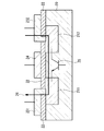
- FIG. 1 is a cross-sectional view showing a configuration example of a semiconductor integrated circuit and a principle that SEL occurs.
- FIG. 2 is a cross-sectional view showing another configuration example of the semiconductor integrated circuit and the principle that SEU or SET occurs.
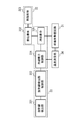
- FIG. 3 is a block circuit diagram showing a configuration example of the electronic device according to the present invention.
- FIG. 1 is a cross-sectional view showing a configuration example of a semiconductor integrated circuit and the principle of generation of SEL. A configuration of the semiconductor integrated circuit shown in FIG. 1 will be described.
- the semiconductor integrated circuit shown in FIG. 1 has an N-type body 10, a source 101, a drain 102, an oxide film 103, and a gate 104. These components operate as a P-type MOS (Metal Oxide Semiconductor: FET) (Field Effect Transistor).
- a power supply terminal 12 for applying a power supply voltage VDD is connected to the source 101.
- a signal terminal 14 for applying a signal voltage Pin is connected to the drain 102.
- the semiconductor integrated circuit shown in FIG. 1 further has a P-type well 11, a drain 111, a source 112, an oxide film 113, and a gate 114. These components operate as N-type MOSFETs.
- a ground terminal 13 for applying a ground voltage VSS is connected to the source 112.
- parasitic diode structure 15 in which the drain 102 functions as an anode and the N-type body 10 functions as a cathode.
- parasitic bipolar transistor structure 16 in which the drain 102 functions as a P-type emitter, the P-type well 11 functions as a P-type collector, and the N-type body 10 functions as an N-type base.
- the source 112 functions as an N-type emitter
- the N-type body 10 functions as an N-type collector
- the P-type well 11 functions as a P-type base.
- a parasitic thyristor structure 18 is also present by combining the parasitic bipolar transistor structure 16 and another parasitic bipolar transistor structure 17.
- a current 19 is generated.
- the current 19 enters the semiconductor integrated circuit from the power supply terminal 12 that applies the power supply voltage VDD to the N-type body 10 and the source 101, passes through the N-type body 10 and the P-type well 11, and the ground voltage VSS is applied to the P-type well 11 and Exit from the ground terminal 13 applied to the source 112.
- SEL is generated by the current 19 flowing through the parasitic thyristor structure 18.
- the current 19 accompanying the SEL flows in a path that is not intended, and causes an error in the operation of the semiconductor integrated circuit.
- FIG. 2 is a cross-sectional view showing another configuration example of the semiconductor integrated circuit and the principle that SEU or SET occurs. A configuration of the semiconductor integrated circuit shown in FIG. 2 will be described.
- the semiconductor integrated circuit shown in FIG. 2 has a P-type body 20, two N-type wells 211 and 212, an insulating layer 22, a source 231, a drain 232, and a gate 24. These components operate as N-type MOSFETs.
- one N-type well 211 functions as an N-type emitter
- the other N-type well 212 functions as an N-type collector
- a P-type body functions as a P-type base.
- a parasitic bipolar transistor structure 25 exists.
- a current 26 is generated.
- the current 26 enters the semiconductor integrated circuit from the drain 232, passes through the N-type well 212, the P-type body 20, and the N-type well 211 and exits from the source 231.
- SEU and SET are generated.
- SEU occurs in a semiconductor integrated circuit functioning as a memory, a flip-flop, or the like, inversion of stored data can be caused.
- SET occurs in a semiconductor integrated circuit functioning as a logic circuit or the like, an undesired current or voltage is generated in a pulse shape, which may cause a malfunction.
- radiation resistance is improved by utilizing the phenomenon that the resistance of the body decreases by cooling the semiconductor integrated circuit. That is, the current generated when charged particles enter the semiconductor integrated circuit is more likely to pass through the body if the resistance of the body is further reduced. As a result, the value of the current flowing through the parasitic thyristor structure and the parasitic bipolar transistor structure becomes smaller.
- it is not necessary to redesign the semiconductor integrated circuit itself.
- FIG. 3 is a block circuit diagram showing a configuration example of the electronic device according to the present invention. A configuration of the electronic device illustrated in FIG. 3 will be described.
- the 3 includes a semiconductor integrated circuit 31, a cooling device 32, a radiation detection device 33, and a temperature measurement unit 34.
- the electronic device shown in FIG. Here, any semiconductor integrated circuit can be used as the semiconductor integrated circuit 31.
- the cooling device 32 includes a cooling element 321, a heat conductor 322, a heat radiator 323, and a cooling element control unit 324.
- the cooling element 321 may be a Peltier element or the like
- the thermal radiator 323 may be a heat sink or the outer wall of an artificial satellite.
- the radiation detection device 33 includes a radiation detection unit 331 and a radiation detection unit control unit 332.
- connection relationship of the components shown in FIG. 3 will be described.
- the electrical connection is indicated by a single line
- the thermal connection is indicated by a double line.
- the semiconductor integrated circuit 31 and the cooling element 321 are thermally connected.
- the cooling element 321 and the heat conductor 322 are thermally connected.
- the heat conductor 322 and the heat radiator 323 are thermally connected.
- the semiconductor integrated circuit 31 and the temperature measuring unit 34 are thermally connected.
- the temperature measurement unit 34 may be built in the semiconductor integrated circuit 31.
- both may be brought into close contact with each other, or the temperature measurement unit 34 may be installed at a position slightly away from the semiconductor integrated circuit 31.
- one temperature measurement unit 34 may be provided for a plurality of semiconductor integrated circuits 31. In any case, the temperature measuring unit 34 is disposed at a position where the temperature of the semiconductor integrated circuit 31 can be measured with a desired accuracy.
- the input and output of the radiation detector 331 are electrically connected to the output and input of the radiation detector controller 332, respectively.
- the other output and other input of the radiation detection unit control unit 332 are electrically connected to the input and output of the cooling element control unit 324, respectively.
- the other input of the cooling element control unit 324 is electrically connected to the output of the temperature measurement unit 34.
- the other output of the cooling element control unit 324 is electrically connected to the input of the cooling element 321.
- the radiation detection unit 331 is preferably arranged at a position sufficiently close to the semiconductor integrated circuit 31 so that the radiation dose affecting the semiconductor integrated circuit 31 can be detected with a desired accuracy.
- Each of the above electrical connections may be connected by two wires by a combination of a signal line and a ground line. At this time, a part of the ground wire may be replaced with a heat conductor 322, a heat radiator 323, or the like.
- the cooling element 321 is controlled by the cooling element control unit 324 to cool the semiconductor integrated circuit 31.
- the heat generated by the cooling is conducted by the heat conductor 322 from the cooling element 321 toward the heat radiator 323.
- the thermal radiator 323 radiates the amount of heat conducted from the thermal conductor 322 toward the outside.
- the radiation detector 331 is controlled by the radiation detector controller 332 to detect the radiation dose.
- the radiation detection unit 331 generates a signal indicating the detection result of the radiation dose, and transmits the signal to the cooling element control unit 324 via the radiation detection unit control unit 332.
- the signal indicating the detection result of the radiation dose may be directly transmitted from the radiation detection unit 331 to the cooling element control unit 324.
- the temperature measuring unit 34 measures the temperature of the semiconductor integrated circuit 31 itself or its surroundings.
- the temperature measurement unit 34 generates a signal indicating the temperature measurement result, and transmits the signal to the cooling element control unit 324.
- the cooling element control unit 324 and the radiation detection unit control unit 332 will be described in more detail.
- the electronic device according to the present invention is, for example, the artificial satellite described above, control that saves power consumption as much as possible is required.
- the Peltier element consumes a lot of electric power in order to transfer the amount of heat from the cooling surface to the high temperature surface. Also, power is consumed for detecting the radiation dose.
- the cooling element control unit 324 may control the cooling capacity of the cooling element 321 according to the combination of the detected radiation dose and the measured temperature.
- the cooling element control unit 324 is only when the detected radiation dose is higher than a predetermined threshold, when the measured temperature is higher than the predetermined threshold, or when these two conditions are met, Control for operating the cooling element 321 may be performed. It is preferable that specific numerical values of these operating conditions and threshold values can be set or changed as appropriate according to the importance of the operation performed by the semiconductor integrated circuit 31 at that time.
- the radiation detection unit control unit 332 may control the radiation detection unit 331 so as to periodically detect radiation, or detect radiation only when the measured temperature is higher than a predetermined threshold. You may perform control which performs.
- the resistance to radiation is improved by utilizing the phenomenon that the resistance of the body decreases by cooling the semiconductor integrated circuit without changing the configuration of the existing semiconductor integrated circuit itself. Furthermore, by appropriately controlling the detection of the radiation dose and the cooling of the semiconductor integrated circuit, the power consumed in these operations can be saved.
- a kit in which components other than the semiconductor integrated circuit 31 in the electronic device shown in FIG. By mounting such a kit so that the cooling element 321 is in close contact with the surface of an arbitrary semiconductor integrated circuit, any existing semiconductor integrated circuit can be improved in radiation resistance.
Landscapes
- Engineering & Computer Science (AREA)
- Health & Medical Sciences (AREA)
- Remote Sensing (AREA)
- Aviation & Aerospace Engineering (AREA)
- General Health & Medical Sciences (AREA)
- Toxicology (AREA)
- Physics & Mathematics (AREA)
- Life Sciences & Earth Sciences (AREA)
- General Physics & Mathematics (AREA)
- Critical Care (AREA)
- Emergency Medicine (AREA)
- Spectroscopy & Molecular Physics (AREA)
- Environmental & Geological Engineering (AREA)
- Biodiversity & Conservation Biology (AREA)
- Environmental Sciences (AREA)
- Molecular Biology (AREA)
- High Energy & Nuclear Physics (AREA)
- Thermal Sciences (AREA)
- Astronomy & Astrophysics (AREA)
- Semiconductor Integrated Circuits (AREA)
- Measurement Of Radiation (AREA)
- Cooling Or The Like Of Semiconductors Or Solid State Devices (AREA)
Abstract
半導体集積回路と、放射線検出装置と、冷却装置とを具備する。ここで、放射線検出装置は、半導体集積回路の付近に設けられて放射線量を検出する。冷却装置は、検出された放射線量に応じて半導体集積回路を冷却する。放射線量がより多い環境では半導体集積回路をより冷却することによって、誤動作の発生を抑制することが出来る。
Description
本発明は電子装置に関し、例えば、放射線に晒される環境で用いられる半導体装置を含む電子装置に好適に利用できるものである。
一般的に使用される半導体集積回路は、比較的大きなエネルギーを有する荷電粒子が当たることで、半導体集積回路の故障や、誤動作などが引き起こされて、重大なエラーが発生し得ることが知られている。
このようなエラーの一例として、SEL(Single Event Latchup:シングルイベントラッチアップ)、SEU(Single Event Upset:シングルイベントアップセット)、SET(Single Event Transient:シングルイベントトランジェント)などが知られている。
これらのエラーの原因は、荷電粒子、及び、放射線によってもたらされる。したがって、宇宙空間で動作する人工衛星や、放射線カメラなどにおいては、内蔵される半導体集積回路が正常に動作するように、放射線によるエラーを抑制する必要がある。
上記に関連して、特許文献1(特開2010-183087号公報)には、半導体回路に係る発明が開示されている。特許文献1に記載の半導体回路は、第1の回路ブロックと、第2の回路ブロックとを備える。ここで、第1の回路ブロックは、複数のpMOSトランジスタを直列又は一のpMOSトランジスタを備えた並列回路に接続して形成されている。第2の回路ブロックは、複数のnMOSトランジスタを直列又は一のnMOSトランジスタを備えた並列回路に接続して形成されている。特許文献1に記載の半導体回路は、第1の回路ブロックと第2の回路ブロックとの接続点を出力端子に接続するとともに、全てのpMOSトランジスタのゲート及び全てのnMOSトランジスタのゲートを共通の入力端子に接続して形成されている。
特許文献1の場合は、半導体集積回路自体の再設計が必要となるので、開発期間およびコストの両方の面で不利である。
本発明では、既存の半導体集積回路において、その構成自体は変えずに、放射線への耐性を向上させる。その他の課題と新規な特徴は、本明細書の記述および添付図面から明らかになるであろう。
一実施の形態による電子装置は、半導体集積回路と、放射線検出装置と、冷却装置とを具備する。ここで、放射線検出装置は、半導体集積回路の付近に設けられて放射線量を検出する。冷却装置は、検出された放射線量に応じて半導体集積回路を冷却する。
前記一実施の形態によれば、放射線量がより多い環境では半導体集積回路をより冷却することによって、誤動作の発生を抑制することが出来る。また、既存の半導体集積回路に冷却装置や放射線検出装置を追加するので、開発期間やコストの面で有利である。
まず、放射線に晒される環境に置かれた半導体集積装置に発生し得る重大エラーについて説明する。
図1は、半導体集積回路の構成例と、SELが発生する原理とを示す断面図である。図1に示した半導体集積回路の構成について説明する。
図1に示した半導体集積回路は、N型ボディー10と、ソース101と、ドレイン102と、酸化膜103と、ゲート104とを有している。これらの構成要素は、P型MOS(Metal Oxide Semiconductor:金属酸化膜半導体)FET(Field Effect Transistor:電界効果トランジスタ)として動作する。ソース101には、電源電圧VDDを印加する電源端子12が接続されている。ドレイン102には、信号電圧Pinを印加する信号端子14が接続されている。
図1に示した半導体集積回路は、さらに、P型ウェル11と、ドレイン111と、ソース112と、酸化膜113と、ゲート114とを有している。これらの構成要素は、N型MOSFETとして動作する。ソース112には、接地電圧VSSを印加する接地端子13が接続されている。
図1に示した半導体集積回路のように、P型MOSFETと、N型MOSFETとが隣接して形成されると、寄生ダイオード構造15、寄生バイポーラトランジスタ構造16、17、寄生サイリスタ構造18などが形成されて、所望しない機能が働いてしまう。
図1に示した構成例では、ドレイン102がアノードとして機能し、N型ボディー10がカソードとして機能する、寄生ダイオード構造15が存在している。
ドレイン102がP型エミッタとして機能し、P型ウェル11がP型コレクタとして機能し、N型ボディー10がN型ベースとして機能する寄生バイポーラトランジスタ構造16が存在している。
ソース112がN型エミッタとして機能し、N型ボディー10がN型コレクタとして機能し、P型ウェル11がP型ベースとして機能する他の寄生バイポーラトランジスタ構造17が存在している。
さらに、上記の寄生バイポーラトランジスタ構造16と、他の寄生バイポーラトランジスタ構造17とが組み合わさって、寄生サイリスタ構造18も存在している。
このような半導体集積回路に、高エネルギーの荷電粒子が入射すると、電流19が発生する。電流19は、電源電圧VDDをN型ボディー10およびソース101に印加する電源端子12から半導体集積回路に侵入し、N型ボディー10およびP型ウェル11を通り、接地電圧VSSをP型ウェル11およびソース112に印加する接地端子13から抜け出る。
この電流19が寄生サイリスタ構造18に流れることによって、SELが発生する。SELに伴う電流19は、本来は意図しない経路に流れており、半導体集積回路の動作にエラーが発生する原因となる。
図2は、半導体集積回路の他の構成例と、SEUまたはSETが発生する原理とを示す断面図である。図2に示した半導体集積回路の構成について説明する。
図2に示した半導体集積回路は、P型ボディー20と、2つのN型ウェル211、212と、絶縁層22と、ソース231と、ドレイン232と、ゲート24とを有している。これらの構成要素は、N型MOSFETとして動作する。
図2に示した半導体集積回路の場合は、一方のN型ウェル211がN型エミッタとして機能し、もう一方のN型ウェル212がN型コレクタとして機能し、P型ボディーがP型ベースとして機能する寄生バイポーラトランジスタ構造25が存在している。
このような半導体集積回路に、高エネルギーの荷電粒子が入射すると、電流26が発生する。電流26は、ドレイン232から半導体集積回路に侵入し、N型ウェル212、P型ボディー20およびN型ウェル211を通り、ソース231から抜け出る。
この電流26が寄生バイポーラトランジスタ構造25に流れることによって、SEUやSETが発生する。メモリやフリップフロップなどとして機能する半導体集積回路にSEUが発生すると、格納されたデータの反転が引き起こされ得る。また、論理回路などとして機能する半導体集積回路にSETが発生すると、所望しない電流や電圧がパルス状に生じて誤動作が引き起こされ得る。
本発明では、半導体集積回路を冷却することでボディーの抵抗が下がる現象を利用して、放射線への耐性を向上させる。すなわち、荷電粒子が半導体集積回路に入射した際に発生する電流は、ボディーの抵抗がより下がればボディーをより通り抜けやすくなる。その結果、寄生サイリスタ構造や寄生バイポーラトランジスタ構造に流れる電流の値もより小さくなる。ここで、本発明によれば半導体集積回路自体の再設計が不要であることに注目されたい。
添付図面を参照して、本発明による電子装置を実施するための形態を以下に説明する。
(実施形態)
図3は、本発明による電子装置の構成例を示すブロック回路図である。図3に示した電子装置の構成について説明する。
図3は、本発明による電子装置の構成例を示すブロック回路図である。図3に示した電子装置の構成について説明する。
図3に示した電子装置は、半導体集積回路31と、冷却装置32と、放射線検出装置33と、温度測定部34とを有している。ここで、半導体集積回路31としては、任意の半導体集積回路が利用可能である。
冷却装置32は、冷却素子321と、熱伝導体322と、熱放射体323と、冷却素子制御部324とを含んでいる。一例として、冷却素子321はペルチェ素子などであっても良いし、熱放射体323はヒートシンクや人工衛星の外壁などであっても良い。
放射線検出装置33は、放射線検出部331と、放射線検出部制御部332とを含んでいる。
図3に示した構成要素の接続関係について説明する。なお、図3では、電気的接続を1本線で示し、熱的接続を2本線で示している。
半導体集積回路31と、冷却素子321とは、熱的に接続されている。冷却素子321と、熱伝導体322とは、熱的に接続されている。熱伝導体322と、熱放射体323とは、熱的に接続されている。これらの熱的な接続を行う際には、例えば、サーマルグリースや接着剤などを介して、接続する面同士を密着させることが好ましい。
半導体集積回路31と、温度測定部34とは、熱的に接続されている。ここで、温度測定部34は、半導体集積回路31に内蔵されていても良い。反対に、温度測定部34が半導体集積回路31から独立している場合は、両者を密着させても良いし、温度測定部34を半導体集積回路31から多少離れた位置に設置しても良い。さらに、複数の半導体集積回路31に対して1つの温度測定部34を設けても良い。いずれの場合も、温度測定部34は、半導体集積回路31の温度を、所望の精度で測定出来るような位置に配置される。
放射線検出部331の入力および出力は、放射線検出部制御部332の出力および入力に、電気的にそれぞれ接続されている。放射線検出部制御部332の他の出力および他の入力は、冷却素子制御部324の入力および出力に、電気的にそれぞれ接続されている。冷却素子制御部324の他の入力は、温度測定部34の出力に電気的に接続されている。冷却素子制御部324の他の出力は、冷却素子321の入力に電気的に接続されている。なお、放射線検出部331は、半導体集積回路31に影響する放射線量を所望の精度で検出できるように、半導体集積回路31から十分に近い位置に配置されることが好ましい。
上記の電気的な接続のそれぞれは、信号線および接地線などの組み合わせによる、2本の配線によって接続しても良い。このとき、接地線の一部は熱伝導体322や熱放射体323などで代用しても良い。
図3に示した構成要素ごとの動作について説明する。
冷却素子321は、冷却素子制御部324に制御されて、半導体集積回路31を冷却する。この冷却に伴って発生する熱量は、熱伝導体322が冷却素子321から熱放射体323に向けて伝導する。熱放射体323は、熱伝導体322から伝導された熱量を、外部に向けて放射する。
放射線検出部331は、放射線検出部制御部332に制御されて、放射線量の検出を行う。放射線検出部331は、放射線量の検出結果を示す信号を生成し、放射線検出部制御部332を介して、冷却素子制御部324に向けて送信する。なお、放射線量の検出結果を示す信号は、放射線検出部331から冷却素子制御部324まで直接伝達されても良い。
温度測定部34は、半導体集積回路31自体またはその周辺の温度を測定する。温度測定部34は、温度の測定結果を示す信号を生成し、冷却素子制御部324に向けて送信する。
冷却素子制御部324および放射線検出部制御部332の動作について、さらに詳細に説明する。本発明による電子装置が、一例として、上述した人工衛星であった場合は、電力の消費を極力節約する制御が必要となる。特に、ペルチェ素子は熱量を冷却面から高温面に移動するために多くの電力を消費する。また、放射線量の検出にも電力は消費される。
そこで、冷却素子制御部324は、検出された放射線量および計測された温度の組み合わせに応じて、冷却素子321の冷却能力を制御しても良い。また、冷却素子制御部324は、検出された放射線量が所定の閾値より高い場合や、計測された温度が所定の閾値より高い場合や、またはこれら2つの条件がそろった場合などに限って、冷却素子321を動作させる制御を行っても良い。これらの動作条件や閾値の具体的な数値は、その時に半導体集積回路31が行っている動作の重要性に応じて、適宜に設定または変更出来ることが好ましい。
また、放射線検出部制御部332は、放射線の検出を定期的に行うように放射線検出部331を制御しても良いし、計測された温度が所定の閾値より高い場合に限って放射線の検出を行うような制御を行っても良い。
このように、本発明では、既存の半導体集積回路自体の構成に変更を加えることなく、半導体集積回路を冷却することでボディーの抵抗が下がる現象を利用して、放射線への耐性を向上させる。さらに、放射線量の検出および半導体集積回路の冷却を適宜に制御することで、これらの動作で消費される電力を節約する。
また、本実施形態のさらなる応用として、図3に示した電子装置のうち、半導体集積回路31以外の構成要素をまとめたキットを用意しても良い。このようなキットを、任意の半導体集積回路の表面に冷却素子321が密着するように装着することで、いかなる既存の半導体集積回路にも放射線への耐性を向上させることが可能となる。
以上、発明者によってなされた発明を実施の形態に基づき具体的に説明したが、本発明は前記実施の形態に限定されるものではなく、その要旨を逸脱しない範囲で種々変更可能であることはいうまでもない。また、前記実施の形態に説明したそれぞれの特徴は、技術的に矛盾しない範囲で自由に組み合わせることが可能である。
10 N型ボディー
101 ソース
102 ドレイン
103 酸化膜
104 ゲート
11 P型ウェル
111 ドレイン
112 ソース
113 酸化膜
114 ゲート
12 電源端子
13 接地端子
14 信号端子
15 寄生ダイオード構造
16 寄生トランジスタ構造
17 寄生トランジスタ構造
18 寄生サイリスタ構造
19 SEL電流
20 P型ボディー
211 N型ウェル
212 N型ウェル
22 絶縁層
231 ソース
232 ドレイン
24 ゲート
25 寄生バイポーラトランジスタ構造
26 SEU電流、SEU電流
31 半導体集積回路
32 冷却装置
321 冷却素子
322 熱伝導体
323 熱放射体
324 冷却素子制御部
33 放射線検出装置
331 放射線検出部
332 放射線検出部制御部
34 温度測定部
101 ソース
102 ドレイン
103 酸化膜
104 ゲート
11 P型ウェル
111 ドレイン
112 ソース
113 酸化膜
114 ゲート
12 電源端子
13 接地端子
14 信号端子
15 寄生ダイオード構造
16 寄生トランジスタ構造
17 寄生トランジスタ構造
18 寄生サイリスタ構造
19 SEL電流
20 P型ボディー
211 N型ウェル
212 N型ウェル
22 絶縁層
231 ソース
232 ドレイン
24 ゲート
25 寄生バイポーラトランジスタ構造
26 SEU電流、SEU電流
31 半導体集積回路
32 冷却装置
321 冷却素子
322 熱伝導体
323 熱放射体
324 冷却素子制御部
33 放射線検出装置
331 放射線検出部
332 放射線検出部制御部
34 温度測定部
Claims (8)
- 任意の半導体集積回路と、
前記半導体集積回路の付近に設けられて放射線量を検出する放射線検出装置と、
検出された前記放射線量に応じて前記半導体集積回路を冷却する冷却装置と
を具備する
電子装置。 - 請求項1に記載の電子装置において、
前記冷却装置は、
前記半導体集積回路と熱的に接続されて、前記半導体集積回路から熱量を吸収する冷却素子と、
前記冷却素子と熱的に接続されて、吸収された前記熱量を伝導する熱伝導体と、
前記熱伝導体と熱的に接続されて、伝導された前記熱量を外部に放射する熱放射体と
を具備する
電子装置。 - 請求項2に記載の電子装置において、
前記半導体集積回路の温度を測定する温度測定部
をさらに具備し、
前記冷却装置は、
測定された前記温度が所定の範囲に含まれるように前記冷却素子の動作を制御する冷却素子制御部
をさらに具備する
電子装置。 - 請求項3に記載の電子装置において、
前記放射線検出装置は、
前記放射線量を検出する放射線検出部と、
前記放射線検出部の動作を制御し、検出された前記放射線量を示す信号を生成して前記冷却素子制御部に伝える放射線検出部制御部と
を具備する
電子装置。 - 任意の半導体集積回路の付近に設けられて放射線量を検出する放射線検出装置と、
前記半導体集積回路に密着するように装着されて、検出された前記放射線量に応じて前記半導体集積回路を冷却する冷却装置と
を具備する
キット。 - 請求項5に記載のキットにおいて、
前記冷却装置は、
前記半導体集積回路と熱的に接続されて、前記半導体集積回路から熱量を吸収する冷却素子と、
前記冷却素子と熱的に接続されて、吸収された前記熱量を伝導する熱伝導体と、
前記熱伝導体と熱的に接続されて、伝導された前記熱量を外部に放射する熱放射体と
を具備する
キット。 - 請求項6に記載のキットにおいて、
前記半導体集積回路の温度を測定する温度測定部
をさらに具備し、
前記冷却装置は、
測定された前記温度が所定の範囲に含まれるように前記冷却素子の動作を制御する冷却素子制御部
をさらに具備する
キット。 - 請求項7に記載のキットにおいて、
前記放射線検出装置は、
前記放射線量を検出する放射線検出部と、
前記放射線検出部の動作を制御し、検出された前記放射線量を示す信号を生成して前記冷却素子制御部に伝える放射線検出部制御部と
を具備する
キット。
Priority Applications (2)
| Application Number | Priority Date | Filing Date | Title |
|---|---|---|---|
| US15/117,805 US10002816B2 (en) | 2014-03-20 | 2015-03-18 | Electronic device |
| EP15765100.1A EP3093884B1 (en) | 2014-03-20 | 2015-03-18 | Electronic device |
Applications Claiming Priority (2)
| Application Number | Priority Date | Filing Date | Title |
|---|---|---|---|
| JP2014-058801 | 2014-03-20 | ||
| JP2014058801A JP6344938B2 (ja) | 2014-03-20 | 2014-03-20 | 電子機器 |
Publications (1)
| Publication Number | Publication Date |
|---|---|
| WO2015141737A1 true WO2015141737A1 (ja) | 2015-09-24 |
Family
ID=54144701
Family Applications (1)
| Application Number | Title | Priority Date | Filing Date |
|---|---|---|---|
| PCT/JP2015/058099 Ceased WO2015141737A1 (ja) | 2014-03-20 | 2015-03-18 | 電子機器 |
Country Status (4)
| Country | Link |
|---|---|
| US (1) | US10002816B2 (ja) |
| EP (1) | EP3093884B1 (ja) |
| JP (1) | JP6344938B2 (ja) |
| WO (1) | WO2015141737A1 (ja) |
Cited By (1)
| Publication number | Priority date | Publication date | Assignee | Title |
|---|---|---|---|---|
| CN110617885A (zh) * | 2019-09-27 | 2019-12-27 | 衢州光明电力投资集团有限公司 | 一种基于远红外线成像的电力设备测温方法 |
Families Citing this family (1)
| Publication number | Priority date | Publication date | Assignee | Title |
|---|---|---|---|---|
| CN108417571B (zh) * | 2018-05-18 | 2024-08-13 | 北京时代华诺科技有限公司 | 一种mos控制晶闸管芯片 |
Citations (2)
| Publication number | Priority date | Publication date | Assignee | Title |
|---|---|---|---|---|
| JPH04211158A (ja) * | 1990-02-14 | 1992-08-03 | Hitachi Ltd | 電子回路の耐放射線保護装置及び人工衛星 |
| JP2002540632A (ja) * | 1999-03-25 | 2002-11-26 | インテル・コーポレーション | 集積回路用の冷却ユニット |
Family Cites Families (5)
| Publication number | Priority date | Publication date | Assignee | Title |
|---|---|---|---|---|
| US5270551A (en) | 1990-02-14 | 1993-12-14 | Hitachi, Ltd. | Method of and apparatus for protecting electronic circuit against radiation |
| JP2002166898A (ja) * | 2000-12-01 | 2002-06-11 | Mitsubishi Heavy Ind Ltd | 宇宙機器の冷却装置 |
| JP5351796B2 (ja) | 2010-02-22 | 2013-11-27 | 三菱重工業株式会社 | 半導体回路 |
| EP2579239A4 (en) * | 2010-05-28 | 2016-01-20 | Nec Display Solutions Ltd | PROJECTION DISPLAY DEVICE |
| US8957385B2 (en) * | 2010-11-29 | 2015-02-17 | Saint-Gobain Ceramics & Plastics, Inc. | Radiation detection system, a radiation sensing unit, and methods of using the same |
-
2014
- 2014-03-20 JP JP2014058801A patent/JP6344938B2/ja active Active
-
2015
- 2015-03-18 US US15/117,805 patent/US10002816B2/en active Active
- 2015-03-18 EP EP15765100.1A patent/EP3093884B1/en active Active
- 2015-03-18 WO PCT/JP2015/058099 patent/WO2015141737A1/ja not_active Ceased
Patent Citations (2)
| Publication number | Priority date | Publication date | Assignee | Title |
|---|---|---|---|---|
| JPH04211158A (ja) * | 1990-02-14 | 1992-08-03 | Hitachi Ltd | 電子回路の耐放射線保護装置及び人工衛星 |
| JP2002540632A (ja) * | 1999-03-25 | 2002-11-26 | インテル・コーポレーション | 集積回路用の冷却ユニット |
Non-Patent Citations (1)
| Title |
|---|
| See also references of EP3093884A4 * |
Cited By (1)
| Publication number | Priority date | Publication date | Assignee | Title |
|---|---|---|---|---|
| CN110617885A (zh) * | 2019-09-27 | 2019-12-27 | 衢州光明电力投资集团有限公司 | 一种基于远红外线成像的电力设备测温方法 |
Also Published As
| Publication number | Publication date |
|---|---|
| EP3093884B1 (en) | 2020-01-29 |
| EP3093884A1 (en) | 2016-11-16 |
| JP2015185596A (ja) | 2015-10-22 |
| US10002816B2 (en) | 2018-06-19 |
| EP3093884A4 (en) | 2017-04-26 |
| JP6344938B2 (ja) | 2018-06-20 |
| US20170011984A1 (en) | 2017-01-12 |
Similar Documents
| Publication | Publication Date | Title |
|---|---|---|
| JP5431994B2 (ja) | 電流制限回路 | |
| JP4843034B2 (ja) | 温度センサ用リングオシレータ、温度センサ回路及びこれを備える半導体装置 | |
| CN104425408B (zh) | 用于3d ic的冷却系统 | |
| JP5547429B2 (ja) | 半導体装置 | |
| US10985744B2 (en) | Apparatus with integrated protection profile and method | |
| US9875950B2 (en) | Semiconductor device | |
| US8514010B2 (en) | Reference current generation circuit and power device using the same | |
| CN104967095B (zh) | 过温保护电路 | |
| US20160133597A1 (en) | Semiconductor device | |
| US20130257329A1 (en) | Junction temperature measurement of a power mosfet | |
| JP2008533734A (ja) | 温度感知機能を有するmosfet | |
| Zhang et al. | Temperature dependence of soft-error rates for FF designs in 20-nm bulk planar and 16-nm bulk FinFET technologies | |
| US9472547B2 (en) | Semiconductor device | |
| JP6344938B2 (ja) | 電子機器 | |
| JP6110615B2 (ja) | リーク電流吸収回路、電圧生成回路、および電源装置 | |
| TWI721045B (zh) | 包含一基材及一第一溫度測量元件的半導體構件以及測定流經一半導體構件之電流的方法以及車輛用的控制單元 | |
| JP4752904B2 (ja) | 温度測定回路、及び、方法 | |
| CN102193604A (zh) | Cpu散热电路 | |
| JP6588229B2 (ja) | 過熱保護回路並びにこれを用いた半導体集積回路装置及び車両 | |
| JP6205238B2 (ja) | 基準電圧発生装置 | |
| JP4553032B2 (ja) | 負荷駆動装置 | |
| JP2009038186A (ja) | 半導体装置 | |
| US12598988B2 (en) | Integrated circuit device | |
| US9117787B2 (en) | Integrated circuit device and method of enabling thermal regulation within an integrated circuit device | |
| Ahmed et al. | 8.8 Fine-Grained Spatial and Temporal Thermal Profiling of a 16nm CMOS Buck Converter and SoC Load-Current Emulator Using Low-Voltage Micron-Scale Thermal Sensors |
Legal Events
| Date | Code | Title | Description |
|---|---|---|---|
| 121 | Ep: the epo has been informed by wipo that ep was designated in this application |
Ref document number: 15765100 Country of ref document: EP Kind code of ref document: A1 |
|
| REEP | Request for entry into the european phase |
Ref document number: 2015765100 Country of ref document: EP |
|
| WWE | Wipo information: entry into national phase |
Ref document number: 2015765100 Country of ref document: EP |
|
| WWE | Wipo information: entry into national phase |
Ref document number: 15117805 Country of ref document: US |
|
| NENP | Non-entry into the national phase |
Ref country code: DE |