WO2015151677A1 - Film conducteur transparent et procédé de fabrication d'un élément conducteur transparent - Google Patents
Film conducteur transparent et procédé de fabrication d'un élément conducteur transparent Download PDFInfo
- Publication number
- WO2015151677A1 WO2015151677A1 PCT/JP2015/055821 JP2015055821W WO2015151677A1 WO 2015151677 A1 WO2015151677 A1 WO 2015151677A1 JP 2015055821 W JP2015055821 W JP 2015055821W WO 2015151677 A1 WO2015151677 A1 WO 2015151677A1
- Authority
- WO
- WIPO (PCT)
- Prior art keywords
- dielectric layer
- transparent conductive
- layer
- conductive member
- metal
- Prior art date
- Legal status (The legal status is an assumption and is not a legal conclusion. Google has not performed a legal analysis and makes no representation as to the accuracy of the status listed.)
- Ceased
Links
Images


Classifications
-
- B—PERFORMING OPERATIONS; TRANSPORTING
- B32—LAYERED PRODUCTS
- B32B—LAYERED PRODUCTS, i.e. PRODUCTS BUILT-UP OF STRATA OF FLAT OR NON-FLAT, e.g. CELLULAR OR HONEYCOMB, FORM
- B32B15/00—Layered products comprising a layer of metal
- B32B15/04—Layered products comprising a layer of metal comprising metal as the main or only constituent of a layer, which is next to another layer of the same or of a different material
-
- G—PHYSICS
- G06—COMPUTING OR CALCULATING; COUNTING
- G06F—ELECTRIC DIGITAL DATA PROCESSING
- G06F3/00—Input arrangements for transferring data to be processed into a form capable of being handled by the computer; Output arrangements for transferring data from processing unit to output unit, e.g. interface arrangements
- G06F3/01—Input arrangements or combined input and output arrangements for interaction between user and computer
- G06F3/03—Arrangements for converting the position or the displacement of a member into a coded form
- G06F3/041—Digitisers, e.g. for touch screens or touch pads, characterised by the transducing means
- G06F3/044—Digitisers, e.g. for touch screens or touch pads, characterised by the transducing means by capacitive means
- G06F3/0445—Digitisers, e.g. for touch screens or touch pads, characterised by the transducing means by capacitive means using two or more layers of sensing electrodes, e.g. using two layers of electrodes separated by a dielectric layer
-
- G—PHYSICS
- G06—COMPUTING OR CALCULATING; COUNTING
- G06F—ELECTRIC DIGITAL DATA PROCESSING
- G06F3/00—Input arrangements for transferring data to be processed into a form capable of being handled by the computer; Output arrangements for transferring data from processing unit to output unit, e.g. interface arrangements
- G06F3/01—Input arrangements or combined input and output arrangements for interaction between user and computer
- G06F3/03—Arrangements for converting the position or the displacement of a member into a coded form
- G06F3/041—Digitisers, e.g. for touch screens or touch pads, characterised by the transducing means
- G06F3/044—Digitisers, e.g. for touch screens or touch pads, characterised by the transducing means by capacitive means
- G06F3/0446—Digitisers, e.g. for touch screens or touch pads, characterised by the transducing means by capacitive means using a grid-like structure of electrodes in at least two directions, e.g. using row and column electrodes
-
- B—PERFORMING OPERATIONS; TRANSPORTING
- B32—LAYERED PRODUCTS
- B32B—LAYERED PRODUCTS, i.e. PRODUCTS BUILT-UP OF STRATA OF FLAT OR NON-FLAT, e.g. CELLULAR OR HONEYCOMB, FORM
- B32B2307/00—Properties of the layers or laminate
- B32B2307/20—Properties of the layers or laminate having particular electrical or magnetic properties, e.g. piezoelectric
- B32B2307/202—Conductive
-
- B—PERFORMING OPERATIONS; TRANSPORTING
- B32—LAYERED PRODUCTS
- B32B—LAYERED PRODUCTS, i.e. PRODUCTS BUILT-UP OF STRATA OF FLAT OR NON-FLAT, e.g. CELLULAR OR HONEYCOMB, FORM
- B32B2307/00—Properties of the layers or laminate
- B32B2307/20—Properties of the layers or laminate having particular electrical or magnetic properties, e.g. piezoelectric
- B32B2307/204—Di-electric
-
- B—PERFORMING OPERATIONS; TRANSPORTING
- B32—LAYERED PRODUCTS
- B32B—LAYERED PRODUCTS, i.e. PRODUCTS BUILT-UP OF STRATA OF FLAT OR NON-FLAT, e.g. CELLULAR OR HONEYCOMB, FORM
- B32B2307/00—Properties of the layers or laminate
- B32B2307/40—Properties of the layers or laminate having particular optical properties
- B32B2307/412—Transparent
-
- B—PERFORMING OPERATIONS; TRANSPORTING
- B32—LAYERED PRODUCTS
- B32B—LAYERED PRODUCTS, i.e. PRODUCTS BUILT-UP OF STRATA OF FLAT OR NON-FLAT, e.g. CELLULAR OR HONEYCOMB, FORM
- B32B2457/00—Electrical equipment
-
- G—PHYSICS
- G06—COMPUTING OR CALCULATING; COUNTING
- G06F—ELECTRIC DIGITAL DATA PROCESSING
- G06F2203/00—Indexing scheme relating to G06F3/00 - G06F3/048
- G06F2203/041—Indexing scheme relating to G06F3/041 - G06F3/045
- G06F2203/04103—Manufacturing, i.e. details related to manufacturing processes specially suited for touch sensitive devices
Definitions
- the present invention relates to a transparent conductive member having a metal layer and a dielectric layer, and a method for manufacturing the transparent conductive member.
- low resistance transparent conductive films are required for various devices such as touch panel materials, liquid crystal displays, plasma displays, inorganic and organic EL (electroluminescence) displays, and solar cells.
- a material constituting such a transparent conductive film for example, metals such as Au, Ag, Pt, Cu, Rh, Pd, Al, Cr, In 2 O 3 , CdO, CdIn 2 O 4 , Cd 2 SnO 4 are used.
- TiO 2 , SnO 2 , ZnO, ITO (indium tin oxide) and other oxide semiconductors are known.
- a wiring made of a transparent conductive film or the like is disposed on the image display surface of the display element.
- the transparent conductive film is required to have high light transmittance.
- a transparent conductive film made of ITO having a high light transmittance is often used in such various display devices.
- a transparent conductive member that aims to achieve both transparency and conductivity by forming layers having a high refractive index on both surfaces of silver serving as a conductive layer (see, for example, Patent Document 1). .
- the present invention provides a transparent conductive member having high productivity and a method for producing the transparent conductive member.
- the transparent conductive member of the present invention includes a first dielectric layer, a second dielectric layer, and a metal layer formed between the first dielectric layer and the second dielectric layer.
- the first dielectric layer and the second dielectric layer contain an infrared absorbing compound.
- the transparent conductive member manufacturing method of the present invention includes a step of forming a first dielectric layer containing an infrared absorbing compound, a step of forming a metal layer on the first dielectric layer, and a metal layer. Forming a second dielectric layer containing an infrared absorbing compound.
- the first dielectric layer and the second dielectric layer contain an infrared absorbing compound. For this reason, by irradiating the laser beam, the first dielectric layer and the second dielectric layer containing the infrared absorbing compound can be etched together with the metal layer. For this reason, by using the transparent conductive member having this configuration, it is possible to easily perform pattern formation of the conductive region and the non-conductive region. That is, a transparent conductive member having high productivity can be provided by forming the transparent conductive member having the above-described configuration.
- the present invention it is possible to provide a transparent conductive member having high productivity and a method for producing the transparent conductive member.
- Embodiment of Transparent Conductive Member (First Embodiment)>
- FIG. 1 and 2 show a schematic configuration (cross-sectional view) of the transparent conductive member of the first embodiment.
- the transparent conductive member 10 having the configuration shown in FIG. 1 has a configuration in which a first dielectric layer 12, a metal layer 13, and a second dielectric layer 14 are laminated in this order.
- a transparent conductive member 10 is provided on the transparent substrate 11.
- the transparent conductive member 10 shown in FIG. 2 a part of the laminated body including the first dielectric layer 12, the metal layer 13, and the second dielectric layer 14 provided on the transparent substrate 11 is subjected to pattern etching. Shows the state. By this pattern etching, the first dielectric layer 12, the metal layer 13, and the second dielectric layer 14 are removed, and the surface of the transparent substrate 11 is exposed from the surface side of the second dielectric layer 14. 15 is provided. By providing the opening 15 in this manner, a transparent region having a conductive region 16 in which the metal layer 13 is continuously formed and a non-conductive region 17 in which the metal layer 13 is not formed and having a desired conductive layer pattern is provided.
- the conductive member 10 can be formed. In the transparent conductive member 10 shown in FIG. 1, the metal layer 13 is formed on the entire surface of the transparent substrate 11. Therefore, the entire region where the metal layer 13 is formed is the conduction region 16.
- the detail of each structure of the transparent conductive member 10 is demonstrated.
- the metal layer 13 is a layer containing a metal for conducting electricity in the transparent conductive member 10.
- the metal layer 13 may be formed on the entire surface of the transparent substrate 11 as shown in FIG. 1, or may be patterned into a desired shape as shown in FIG.
- the metal contained in the metal layer 13 is not particularly limited as long as it is a highly conductive metal, and examples thereof include silver, copper, gold, platinum group, titanium, and chromium.
- the metal layer 13 may contain only one kind of these metals or two or more kinds.
- the metal contained in the metal layer 13 is preferably silver or an alloy containing 90 atomic% or more of silver.
- the metal combined with silver include zinc, gold, copper, palladium, aluminum, manganese, bismuth, neodymium, and molybdenum.
- a combination of silver and zinc is preferable because the sulfidation resistance of the metal layer 13 is increased.
- a combination of silver and gold is preferable because salt resistance (NaCl) resistance is increased.
- oxidation resistance is increased, which is preferable.
- the plasmon absorption rate of the metal layer 13 is preferably 10% or less, more preferably 7% or less, and further preferably 5% or less over the wavelength range of 400 to 800 nm (over the entire range). If there is a region having a large plasmon absorption rate in a part of the wavelength of 400 to 800 nm, the transmitted light of the conductive region 16 of the transparent conductive member 10 is likely to be colored.
- the plasmon absorption rate at a wavelength of 400 to 800 nm of the metal layer 13 is measured by the following procedures (i) to (iii).
- platinum palladium is formed to a thickness of 0.1 nm by a BMC-800T vapor deposition apparatus manufactured by SYNCHRON.
- the average thickness of platinum palladium is calculated from the formation rate of the manufacturer's nominal value of the vapor deposition apparatus.
- a metal layer having a thickness of 20 nm is formed on the substrate to which platinum palladium is adhered by vacuum deposition.
- the thickness of the metal layer 13 is preferably 10 nm or less, more preferably in the range of 3 to 9 nm, and still more preferably in the range of 5 to 8 nm.
- the metal layer 13 is less likely to reflect the original metal.
- the optical admittance of the transparent conductive member 10 by the first dielectric layer 12 and the second dielectric layer 14 can be easily adjusted, and light on the surface of the conductive region 16 can be adjusted. It is easy to suppress reflection.
- the thickness of the metal layer 13 can be obtained by measurement using an ellipsometer.
- the metal layer 13 may be a layer formed by any method, but is preferably a layer formed by a vacuum deposition method. If it is a vacuum evaporation method, the transparent substrate 11 will not be exposed to a high temperature environment, but the metal layer 13 with high planarity can be formed very quickly.
- the underlayer becomes a growth nucleus when the metal layer 13 is formed, so that the metal layer 13 tends to be a smooth film. As a result, even if the metal layer 13 is thin, plasmon absorption hardly occurs.
- the patterning method is not particularly limited.
- the metal layer 13 may be a layer formed by arranging a mask having a desired pattern, or may be a layer patterned by a known etching method.
- the first dielectric layer 12 and the second dielectric layer 14 are layers that adjust the light transmittance (optical admittance) of the conductive region 16 of the transparent conductive member 10, that is, the region where the metal layer 13 is formed. At least the conductive region 16 of the transparent conductive member 10 is formed. Although the first dielectric layer 12 and the second dielectric layer 14 may be formed also in the non-conductive region 17 of the transparent conductive member 10, a pattern composed of the conductive region 16 and the non-conductive region 17 is visually recognized. From the viewpoint of making it difficult, it is preferably formed only in the conductive region 16 and removed from the non-conductive region 17 as shown in FIG.
- the first dielectric layer 12 and the second dielectric layer 14 contain an infrared absorbing compound.
- the infrared absorbing compound included in the first dielectric layer 12 and the second dielectric layer 14 include ZnO, AZO, IZO, GZO, tin oxide, ATO, ITO, lanthanum boride, and nickel complex. Systemic compounds and the like can be used.
- Specific product names include: zinc oxide series, Cellax series (manufactured by Nissan Chemical Industries, Ltd.), passest series (manufactured by Hakusui Tech Co., Ltd.), tin oxide series, ATO dispersion, ITO dispersion (manufactured by Mitsubishi Materials) And KH series (manufactured by Sumitomo Metal Mining Co., Ltd.).
- an organic compound such as an imonium compound, a phthalocyanine compound, or an aminium compound can be used as the infrared absorbing compound contained in the first dielectric layer 12 and the second dielectric layer 14.
- Specific product names include NIR-IM1, NIR-AM1 (manufactured by Nagase Chemitex), Lumogen series (manufactured by BASF), and the like.
- the first dielectric layer 12 and the second dielectric layer 14 include a dielectric material having a refractive index higher than that of the transparent substrate 11 described later, or an oxide semiconductor material.
- the refractive index of light having a wavelength of 570 nm of the dielectric material or the oxide semiconductor material is preferably 0.1 to 1.1 larger than the refractive index of light having a wavelength of 570 nm of the transparent substrate 11, and 0.4 to 1 It is more preferable that the value be larger by 0.0.
- the value of the refractive index measured in a 25 degreeC environment is used for a refractive index.
- the refractive index can be determined by measuring using a commercially available ellipsometer.
- the specific refractive index of light having a wavelength of 570 nm of the dielectric material or oxide semiconductor material included in the first dielectric layer 12 and the second dielectric layer 14 is preferably greater than 1.5. It is more preferably from 7 to 2.5, still more preferably from 1.8 to 2.5.
- the refractive index of the dielectric material or the oxide semiconductor material is larger than 1.5, the first dielectric layer 12 and the second dielectric layer 14 cause the optical admittance of the conductive region 16 of the transparent conductive member 10. Is fully adjusted.
- the refractive index of the 1st dielectric material layer 12 and the 2nd dielectric material layer 14 is adjusted with the refractive index of the material contained, and the density of material.
- the first dielectric layer 12 and the second dielectric layer 14 include zinc sulfide, metal oxide, inorganic oxide, a mixture of zinc sulfide and metal oxide, a mixture of zinc sulfide and inorganic oxide, titanium oxide ( TiO 2 ), gallium-doped tin oxide (GZO), zinc oxide (ZnO), aluminum-doped zinc oxide, antimony-doped tin oxide (ATO), antimony-doped zinc oxide (AZO), indium-doped tin oxide (ITO) ), Indium-doped zinc oxide (IZO), or the like can be used.
- Examples of the metal oxide and inorganic oxide that can be used together with zinc sulfide include TiO 2 , ITO (indium tin oxide), ZnO, Nb 2 O 5 , ZrO 2 , CeO 2 , Ta 2 O 5 , and Ti 3 O.
- silicon dioxide (SiO 2 ) is particularly preferable.
- a metal fluoride can be used for the first dielectric layer 12 and the second dielectric layer 14.
- the metal fluoride include LaF 3 , BaF 2 , Na 5 Al 3 F 14 , Na 3 AlF 6 , AlF 3 , MgF 2 , CaF 2 , CeF 3 , NdF 3 , and YF 3 .
- metal nitride can be used for the first dielectric layer 12 and the second dielectric layer 14.
- the metal nitride include boron nitride, aluminum nitride, chromium nitride, silicon nitride, tungsten nitride, magnesium nitride, molybdenum nitride, lithium nitride, and titanium nitride.
- the first dielectric layer 12 and the second dielectric layer 14 preferably contain at least zinc sulfide (ZnS) as a dielectric material. Since the first dielectric layer 12 and the second dielectric layer 14 contain zinc sulfide, moisture from the transparent substrate 11 side or the like passes through the first dielectric layer 12 and the second dielectric layer 14. It becomes difficult and corrosion of the metal layer 13 is suppressed.
- ZnS zinc sulfide
- the first dielectric layer 12 and the second dielectric layer 14 are at least one selected from metal oxides, inorganic oxides, metal fluorides, and metal nitrides together with zinc sulfide. By co-evaporating this compound, the first dielectric layer 12 and the second dielectric layer 14 are likely to be amorphous, and the flexibility of the transparent conductive member 10 is likely to be enhanced.
- the average content of zinc sulfide is within the range of 0.5 to 99 mass% with respect to the total number of moles of the material constituting the layer. It is preferably within a range of 50 to 95% by mass, and more preferably within a range of 60 to 85% by mass.
- the ratio of zinc sulfide is high, the co-evaporation rate is increased, and the formation rate of the first dielectric layer 12 and the second dielectric layer 14 is increased.
- the ratio of zinc sulfide is high, the refractive index is increased, and light absorption in the metal layer 13 can be reduced.
- the amorphousness of the first dielectric layer 12 and the second dielectric layer 14 is increased, and the first dielectric layer 12 and the second dielectric layer are increased. The occurrence of 14 cracks is suppressed.
- the second dielectric layer 14 thickness T B is preferably in the range of 10 ⁇ 150 nm, more preferably in the range of 10 ⁇ 80 nm.
- the thickness of the first dielectric layer 12 and the second dielectric layer 14 is 150 nm or less, the light in the region where the first dielectric layer 12 and the second dielectric layer 14 are formed.
- the permeability is difficult to decrease.
- the thicknesses of the first dielectric layer 12 and the second dielectric layer 14 are measured with an ellipsometer.
- the first dielectric layer 12 and the second dielectric layer 14 are preferably formed by a co-evaporation method.
- the vapor deposition method include a resistance heating vapor deposition method, an electron beam vapor deposition method, an ion plating method, and an ion beam vapor deposition method.
- a vapor deposition apparatus for example, a BMC-800T vapor deposition machine manufactured by SYNCHRON Co., Ltd. can be used.
- the second dielectric layer 14 is selected from zinc sulfide, metal oxide, inorganic oxide, metal fluoride, and metal nitride. It is preferable to form a layer formed by co-evaporation with at least one compound.
- the first dielectric layer 12 and the second dielectric layer 14 are both co-evaporated with zinc sulfide and at least one compound selected from metal oxide, inorganic oxide, metal fluoride and metal nitride. It may be a layer formed by a method.
- Transparent substrate As the transparent substrate 11, materials applied to transparent substrates of various display devices can be used.
- the transparent substrate 11 is a glass substrate, a cellulose ester resin (for example, triacetyl cellulose (abbreviation: TAC), diacetyl cellulose, acetylpropionyl cellulose, etc.), a polycarbonate resin (for example, Panlite, Multilon (manufactured by Teijin Ltd.)).
- a cellulose ester resin for example, triacetyl cellulose (abbreviation: TAC), diacetyl cellulose, acetylpropionyl cellulose, etc.
- a polycarbonate resin for example, Panlite, Multilon (manufactured by Teijin Ltd.)
- Cycloolefin resins for example, ZEONOR (manufactured by ZEON CORPORATION), ARTON (manufactured by JSR), APPEL (manufactured by Mitsui Chemicals)), acrylic resins (for example, polymethyl methacrylate, acrylite (manufactured by Mitsubishi Rayon), Sumipex) (Manufactured by Sumitomo Chemical Co., Ltd.)), polyimide, phenol resin, epoxy resin, polyphenylene ether (abbreviation: PPE) resin, polyester resin (for example, polyethylene terephthalate (abbreviation: PET), polyethylene naphthalate (abbreviation: PEN)), polyether Rusulfone resin, acrylonitrile / butadiene / styrene resin (abbreviation: ABS resin) / acrylonitrile / styrene resin (abbreviation: AS resin), methyl methacrylate / buta
- the transparent substrate 11 to be applied includes a glass substrate, a cellulose ester resin, a polycarbonate resin, a polyester resin (particularly polyethylene terephthalate), a triacetyl cellulose, a cycloolefin resin, a phenol resin, Consists of resin components such as epoxy resin, polyphenylene ether (PPE) resin, polyethersulfone, ABS / AS resin, MBS resin, polystyrene, methacrylic resin, polyvinyl alcohol / EVOH (ethylene vinyl alcohol resin), styrene block copolymer resin, etc. It is preferable that it is a film.
- the transparent substrate 11 preferably has high transparency to visible light, and the average transmittance of light having a wavelength of 450 to 800 nm is preferably 70% or more, more preferably 80% or more, and 85% or more. More preferably it is. When the average light transmittance of the transparent substrate 11 is 70% or more, the light transmittance of the transparent conductive member 10 is likely to be increased.
- the average absorption rate of light with a wavelength of 450 to 800 nm of the transparent substrate 11 is preferably 10% or less, more preferably 5% or less, and further preferably 3% or less.
- the average transmittance is measured by making light incident from an angle inclined by 5 ° with respect to the normal line of the surface of the transparent substrate 11.
- the average absorptance is measured by measuring the average reflectance of the transparent substrate 11 by making light incident from the same angle as the average transmittance.
- Average absorptivity 100 ⁇ (average transmittance + average reflectance) Calculate as The average transmittance and the average reflectance can be measured using a spectrophotometer (for example, U4100: manufactured by Hitachi High-Technologies Corporation).
- the refractive index of light having a wavelength of 570 nm of the transparent substrate 11 is preferably in the range of 1.30 to 1.95, more preferably in the range of 1.35 to 1.75, and still more preferably 1.35. Within the range of ⁇ 1.70.
- the refractive index of the transparent substrate 11 is usually determined by the material of the transparent substrate 11.
- the refractive index of the transparent substrate 11 can be determined by measuring in an environment of 25 ° C. using an ellipsometer.
- the haze value of the transparent substrate 11 is preferably in the range of 0.01 to 2.5, and more preferably in the range of 0.1 to 1.2. It is preferable that the haze value of the transparent substrate is 2.5 or less because the haze value as the transparent conductive member can be suppressed.
- the haze value can be measured using a haze meter.
- the thickness of the transparent substrate 11 is preferably in the range of 1 ⁇ m to 20 mm, more preferably in the range of 10 ⁇ m to 2 mm. If the thickness of the transparent substrate 11 is 1 ⁇ m or more, the strength of the transparent substrate 11 is increased, and it is possible to prevent the first dielectric layer 12 from being cracked or torn during production. On the other hand, if the thickness of the transparent substrate 11 is 20 mm or less, sufficient flexibility of the transparent conductive member 10 can be obtained. Furthermore, the thickness of the electronic device apparatus etc. which comprised the transparent conductive member 10 can be made thin. Moreover, the electronic device apparatus etc. using the transparent conductive member 10 can also be reduced in weight.
- the transparent substrate 11 is preferably used in a forming step after removing moisture and remaining solvent contained in the substrate in advance using a cryopump or the like before forming each constituent layer.
- a known clear hard coat (CHC) layer may be provided on the transparent substrate 11 from the viewpoints of hardness, smoothness, and oligomer activity prevention of the first dielectric layer 12 to be formed later. Further, from the viewpoint of the function of the back surface of the transparent substrate 11, a CHC layer may be provided on the back surface of the transparent substrate 11.
- the CHC layer thermosetting silicon, epoxy, acrylic, or polysilazane can be used, but any CHC layer may be used as long as hardness, smoothness, haze, and adhesion with the upper layer are obtained.
- an ultraviolet curable acrylic resin from the viewpoint of productivity and safety.
- the film thickness of the CHC layer is preferably 0.1 ⁇ m or more and 10 ⁇ m or less in consideration of the balance of curl, hardness, and cracking.
- the transparent conductive member 10 may include an underlayer that becomes a growth nucleus when the metal layer 13 is formed, as necessary.
- the underlayer is a layer formed on the transparent substrate 11 side of the metal layer 13 and adjacent to the metal layer 13, and the metal layer 13 is preferably formed directly on the underlayer.
- the underlayer is preferably formed at least in the conductive region 16 of the transparent conductive member, and may be formed in the non-conductive region 17 of the transparent conductive member 10.
- the smoothness of the surface of the metal layer 13 is increased even when the metal layer 13 is thin. The reason is as follows.
- the material of the metal layer 13 is deposited on the first dielectric layer 12 by a general vacuum deposition method
- atoms attached on the first dielectric layer 12 migrate (move) at the initial stage of formation.
- a film grows clinging to this lump. Therefore, in the film at the initial stage of formation, there is a gap between the lumps, and the film is not conductive.
- a lump further grows from this state, a part of the lump is connected and barely conducted.
- plasmon absorption occurs.
- the lumps are completely connected and plasmon absorption is reduced.
- the intrinsic reflection of the metal occurs, and the light transmittance of the film decreases.
- the metal layer 13 grows using the base layer as a growth nucleus. That is, the material of the metal layer 13 is difficult to migrate, and the film grows without forming the above-described sea-island structure. As a result, it becomes easy to obtain a smooth metal layer 13 even if the thickness is small.
- the underlayer preferably contains palladium, molybdenum, zinc, germanium, niobium or indium, an alloy of these metals with other metals, an oxide or sulfide of these metals (for example, ZnS). .
- the underlayer may contain only one kind or two or more kinds.
- the amount of palladium, molybdenum, zinc, germanium, niobium or indium contained in the underlayer is preferably 20% by mass or more, more preferably 40% by mass or more, and further preferably 60% by mass or more.
- the underlayer contains palladium or molybdenum.
- the metal that forms an alloy with palladium, molybdenum, zinc, germanium, niobium, or indium is not particularly limited.
- a platinum group other than palladium, gold, cobalt, nickel, titanium, aluminum, chromium, and the like can be used.
- the thickness of the underlayer is preferably 3 nm or less, more preferably 0.5 nm or less, and particularly preferably a monoatomic film.
- the underlayer may be in a state where metal atoms are separated from each other and attached to the surface to be formed. If the adhesion amount of the underlayer is 3 nm or less, the underlayer is unlikely to affect the light transmittance and optical admittance of the transparent conductive member 10. The presence or absence of the underlayer is confirmed by the ICP-MS method. Further, the thickness of the underlayer is calculated from the product of the formation speed and the formation time.
- the underlayer is preferably a layer formed by vapor deposition or sputtering.
- the vapor deposition method includes a vacuum vapor deposition method, an electron beam vapor deposition method, an ion plating method, an ion beam vapor deposition method and the like.
- the deposition time is appropriately selected according to the desired thickness of the underlying layer and the formation speed.
- the deposition rate is preferably 0.01 to 1.5 nm / second, more preferably 0.01 to 0.7 nm / second.
- the patterning method is not particularly limited.
- the underlayer may be, for example, a layer formed in a pattern by a vapor phase forming method by placing a mask having a desired pattern on the surface to be formed, or a layer patterned by a known etching method. There may be. Further, the metal film 13, the first dielectric layer 12, and the second dielectric layer 14 may be patterned by laser etching simultaneously.
- the transparent conductive member 10 may have a low refractive index layer (not shown) for adjusting the light transmittance (optical admittance) of the conductive region 16 of the transparent conductive member 10 on the second dielectric layer 14. Good.
- the low refractive index layer may be formed only in the conductive region 16 of the transparent conductive member 10, or may be formed in both the conductive region 16 and the non-conductive region 17 of the transparent conductive member 10.
- the low refractive index layer includes a dielectric material that is included in the first dielectric layer 12 and the second dielectric layer 14, or a dielectric material having a refractive index of light having a wavelength of 570 nm lower than that of the oxide semiconductor material, or And oxide semiconductor materials.
- the refractive index of light with a wavelength of 570 nm of the dielectric material or oxide semiconductor material contained in the low refractive index layer is the refraction of light with a wavelength of 570 nm of the material contained in the first dielectric layer 12 and the second dielectric layer 14.
- the ratio is preferably 0.2 or more and more preferably 0.4 or more, respectively.
- the average transmittance of light having a wavelength of 450 to 800 nm of the transparent conductive member 10 is preferably 83% or more in both the conductive region 16 and the non-conductive region 17, more preferably 85% or more, and still more preferably. It is 88% or more.
- the transparent conductive member 10 can be applied to applications requiring high transparency to visible light.
- the average transmittance of light having a wavelength of 400 to 1000 nm of the transparent conductive member 10 is preferably 80% or more in both the conductive region 16 and the non-conductive region 17, more preferably 83% or more, and still more preferably. 85% or more.
- the transparent conductive member 10 is used in applications requiring transparency with respect to light in a wide wavelength range, such as a transparent conductive film for solar cells. Can be applied.
- the average absorptance of light having a wavelength of 400 to 800 nm of the transparent conductive member 10 is preferably 10% or less, more preferably 8% or less, and even more preferably in both the conductive region 16 and the non-conductive region 17. 7% or less.
- the maximum value of the light absorptance of the transparent conductive member 10 having a wavelength of 450 to 800 nm is preferably 15% or less, more preferably 10% or less, in both the conducting region 16 and the non-conducting region 17. More preferably, it is 9% or less.
- the average reflectance of light having a wavelength of 500 to 700 nm of the transparent conductive member 10 is preferably 20% or less, more preferably 15% or less, in both the conductive region 16 and the non-conductive region 17. More preferably, it is 10% or less.
- the average transmittance, average absorption rate, and average reflectance are preferably the average transmittance, average absorption rate, and average reflectance measured in the usage environment of the transparent conductive member 10.
- a layer made of the organic resin may be disposed on the transparent conductive member 10 to measure average transmittance and average reflectance.
- the transparent conductive member 10 is used in the air, it is preferable to measure the average transmittance and the average reflectance in the air.
- the transmittance and the reflectance are measured with a spectrophotometer by making measurement light incident from an angle inclined by 5 ° with respect to the normal line of the surface of the transparent conductive member 10.
- the absorptance is calculated by a calculation formula of [100 ⁇ (transmittance + reflectance)].
- the transparent conductive member 10 has the conductive region 16 and the non-conductive region 17 as shown in FIG. 2, it is preferable that the reflectivity of the conductive region 16 and the reflectivity of the non-conductive region 17 are approximated.
- the difference ⁇ R between the luminous reflectance of the conductive region 16 and the luminous reflectance of the non-conductive region 17 is preferably 5% or less, more preferably 3% or less, and even more preferably. Is 1% or less, particularly preferably 0.3% or less.
- the luminous reflectance of the conductive region 16 and the non-conductive region 17 is preferably 5% or less, more preferably 3% or less, and even more preferably 1% or less.
- the luminous reflectance is a Y value measured with a spectrophotometer (U4100; manufactured by Hitachi High-Technologies Corporation).
- the transparent conductive member 10 includes the conductive region 16 and the non-conductive region 17, the a * value and the b * value in the L * a * b * color system must be within ⁇ 30 in any region. Is preferable, more preferably within ⁇ 5, still more preferably within ⁇ 3.0, and particularly preferably within ⁇ 2.0. If the a * value and b * value in the L * a * b * color system are within ⁇ 30, both the conductive region 16 and the non-conductive region 17 are observed as colorless and transparent. The a * value and b * value in the L * a * b * color system are measured with a spectrophotometer.
- the surface electrical resistance of the conductive region 16 of the transparent conductive member 10 is 50 ⁇ / sq. Or less, more preferably 30 ⁇ / sq. It is as follows.
- the surface electric resistance value of the conduction region 16 is 50 ⁇ / sq.
- the following transparent conductive member 10 can be applied to a transparent conductive panel for a capacitive touch panel.
- the surface electrical resistance value of the conduction region 16 is adjusted by the thickness of the metal layer 13 and the like.
- the surface electrical resistance value of the conduction region 16 is measured in accordance with, for example, JIS K7194, ASTM D257, or the like. It is also measured by a commercially available surface electrical resistivity meter.
- Embodiment of Transparent Conductive Member (Second Embodiment)> Next, a second embodiment of the transparent conductive member will be described. 3 and 4 show a schematic configuration (cross-sectional view) of the transparent conductive member of the second embodiment. FIG. 4 is a modification of the embodiment shown in FIG.
- the transparent conductive member 20 of the second embodiment shown in FIG. 3 has a configuration in which a first dielectric layer 12, a first antisulfurization layer 18, a metal layer 13, and a second dielectric layer 14 are laminated in this order. is doing.
- a transparent conductive member 20 is provided on the transparent substrate 11.
- the transparent conductive member 20A of the modified example of the second embodiment shown in FIG. 4 includes a first dielectric layer 12, a first sulfidation preventing layer 18, a metal layer 13, a second sulfidation preventing layer 19, and a second dielectric. It has the structure which laminated
- a transparent conductive member 20 ⁇ / b> A is provided on the transparent substrate 11.
- the same configuration as that of the transparent conductive member of the first embodiment described above can be applied except that the first sulfide prevention layer 18 and the second sulfide prevention layer 19 are provided. .
- the first sulfide prevention layer 18 and the second sulfide prevention layer 19 are provided.
- a desired conductive layer pattern can be formed.
- the first sulfidation preventing layer 18 and the second sulfidation preventing layer 19 are also removed together with the first dielectric layer 12, the metal layer 13, and the second dielectric layer 14. It is preferable.
- the first dielectric layer 12 or the second dielectric layer 14 preferably contains zinc sulfide. Therefore, for example, when the first dielectric layer 12 is a layer containing zinc sulfide, as shown in FIG. 3, the first anti-sulfurization layer 18 is provided between the first dielectric layer 12 and the metal layer 13. It is preferable to form.
- the first sulfidation preventing layer 18 may be formed also in the non-conductive region of the transparent conductive members 20 and 20A. However, from the viewpoint of making it difficult to visually recognize the pattern including the conductive region 16 and the non-conductive region. It is preferable to form only in.
- the first sulfidation preventing layer 18 can be configured as a layer containing metal oxide, inorganic oxide, metal nitride, metal fluoride, or the like, or Zn.
- the first sulfurization preventing layer 18 may contain only one kind or two or more kinds, but preferably contains a compound containing a zinc metal element.
- the first sulfidation is performed by a compound capable of reacting with sulfur or adsorbing sulfur. It is preferable that the prevention layer 18 is formed.
- the metal oxide is a compound that reacts with sulfur
- the reaction product of the metal oxide and sulfur preferably has high visible light permeability.
- Metal oxides, inorganic oxides, metal nitrides, and metal fluorides that can be applied to the first antisulfurization layer 18 are described in the description of the first dielectric layer 12 and the second dielectric layer 14, Mention may be made of compounds similar to metal oxides, metal nitrides, and metal fluorides.
- Zn, ZnO, IZO (indium oxide / zinc oxide), and GZO (gallium-doped zinc oxide) are preferable.
- the thickness of the first sulfidation preventing layer 18 is a thickness capable of protecting the surface of the first dielectric layer 12 from an impact when the metal layer 13 is formed.
- zinc sulfide that can be included in the first dielectric layer 12 has a high affinity with the metal included in the metal layer 13. Therefore, if the thickness of the first sulfidation prevention layer 18 is very thin and a part of the first dielectric layer 12 is exposed, the metal layer 13 grows around the exposed part, and the metal layer 13 Tends to be dense.
- the first sulfidation preventing layer 18 is preferably relatively thin, preferably in the range of 0.1 to 15 nm, more preferably in the range of 0.5 to 10 nm, and even more preferably 1 to 5 nm. Is within the range.
- the thickness of the first sulfurization preventive layer 18 can be measured using an ellipsometer.
- the first antisulfurization layer 18 can be formed by a general vapor deposition method such as a vacuum deposition method, a sputtering method, an ion plating method, a plasma CVD method, a thermal CVD method, etc. It is preferable to do.
- a general vapor deposition method such as a vacuum deposition method, a sputtering method, an ion plating method, a plasma CVD method, a thermal CVD method, etc. It is preferable to do.
- the first sulfidation preventing layer 18 may be a layer formed in a pattern by a vapor phase forming method by placing a mask having a desired pattern on the surface to be formed, and patterned by a known etching method, for example. It may be a layer formed. Further, the metal film 13, the first dielectric layer 12, and the second dielectric layer 14 may be patterned by laser etching simultaneously.
- a second antisulfurization layer 19 is provided between the metal layer 13 and the second dielectric layer 14.
- a formed configuration is preferable.
- the second sulfidation preventing layer 19 may be formed also in the non-conductive region of the transparent conductive member 10, but from the viewpoint of making it difficult to visually recognize the pattern composed of the conductive region 16 and the non-conductive region, only the conductive region 16 is provided. Preferably it is formed.
- the same constituent materials and the same construction method as those of the first sulfidation preventing layer 18 can be applied.
- the thickness of the second antisulfurization layer 19 is preferably a thickness that can protect the surface of the metal layer 13 from impact during the formation of the second dielectric layer 14.
- the thickness of the second antisulfurization layer 19 is very thin, and a part of the metal layer 13 is present. If even a slight amount is exposed, the adhesion between the metal layer 13 or the second antisulfurization layer 19 and the second dielectric layer 14 is likely to increase.
- the specific thickness of the second antisulfurization layer 19 is preferably 0.1 to 10 nm, more preferably 0.5 to 5 nm, and further preferably 1 to 3 nm.
- the thickness of the second sulfurization preventing layer 19 is measured with an ellipsometer.
- the transparent conductive member can be produced using a general vapor deposition method such as a known vacuum deposition method, sputtering method, ion plating method, plasma CVD method, and thermal CVD method. Moreover, it can also produce using general coating liquid phase methods, such as a gravure coat and a die coat.
- a general vapor deposition method such as a known vacuum deposition method, sputtering method, ion plating method, plasma CVD method, and thermal CVD method.
- general coating liquid phase methods such as a gravure coat and a die coat.
- the first dielectric layer 12 is preferably a layer formed by an electron beam evaporation method or a sputtering method.
- the sputtering method since the material collides with the deposition target at high speed during film formation, a dense and smooth film is easily obtained, and the light transmittance of the metal layer 13 is likely to be increased. Further, when the metal layer 13 is a film formed by sputtering, the metal layer 13 is hardly corroded even in a high temperature and low humidity environment.
- the type of the sputtering method is not particularly limited, and may be an ion beam sputtering method, a magnetron sputtering method, a reactive sputtering method, a bipolar sputtering method, a bias sputtering method, a counter sputtering method, or the like.
- the metal layer 13 is particularly preferably a film formed by a counter sputtering method.
- the metal layer 13 becomes dense and the surface smoothness is likely to increase.
- the surface electrical resistance of the metal layer 13 becomes lower and the light transmittance is likely to increase.
- IAD ion assist
- the transparent conductive member is preferably produced by a continuous process from the viewpoint of production efficiency.
- FIG. 5 shows an example of a manufacturing flow of a transparent conductive member for manufacturing the transparent conductive member in a continuous online process. Below, the manufacturing method of a transparent conductive member using the manufacturing flow shown in FIG. 5 is demonstrated.
- the transparent conductive member 20 ⁇ / b> A according to the modification of the second embodiment shown in FIG. 4, the first dielectric layer 12, the first antisulfurization layer 18, and the metal layer are formed on the transparent substrate 11. 13, the manufacturing method which laminates
- step 1 the first dielectric layer 12 is formed on the transparent substrate 11 in the vacuum deposition chamber 21.
- step 2 the first sulfidation prevention layer 18 is formed on the first dielectric layer 12 in the vacuum deposition chamber 21.
- step 3 the metal layer 13 is formed on the first sulfurization prevention layer 18 in the vacuum deposition chamber 21.
- step 4 a second antisulfurization layer 19 is formed on the metal layer 13 in the vacuum deposition chamber 21.
- the second dielectric layer 14 is formed on the second sulfurization prevention layer 19 in the vacuum deposition chamber 21.
- the first resistance heating boat 22 is loaded with a dielectric material, for example, zinc sulfide, and the second resistance heating boat 23 is loaded with an infrared absorbing material, metal oxide, inorganic oxide, metal fluoride, and metal nitridation. At least one compound selected from the product, for example, SiO 2 is loaded. Then, each target is energized and heated, and the first dielectric layer 12 is formed on the continuously transported transparent substrate 11 by a co-evaporation method.
- a dielectric material for example, zinc sulfide
- the second resistance heating boat 23 is loaded with an infrared absorbing material, metal oxide, inorganic oxide, metal fluoride, and metal nitridation.
- At least one compound selected from the product, for example, SiO 2 is loaded.
- each target is energized and heated, and the first dielectric layer 12 is formed on the continuously transported transparent substrate 11 by a co-evaporation method.
- each resistance heating boat first resistance heating boat 22, second resistance heating boat 23
- zinc sulfide and metal oxide, inorganic oxide, metal fluoride In addition, the ratio of at least one compound selected from metal nitrides and the ratio in the layer can be adjusted.
- step 2 the resistance heating boat 24 is charged with a material for forming the first sulfidation prevention layer 18, for example, ZnO. Then, the first sulfidation prevention layer 18 is formed on the first dielectric layer 12 of the transparent substrate 11 that is continuously conveyed by energization heating under a predetermined condition.
- Step 3 the resistance heating boat 25 is charged with a material for forming the metal layer 13, for example, Ag. And the metal layer 13 is formed on the 1st sulfurization prevention layer 18 of the transparent substrate 11 currently conveyed by carrying out electricity heating on predetermined conditions.
- the metal layer 13 is formed of silver and the formation rate of the silver layer is 0.3 nm / second or more. From the viewpoint of realizing higher productivity, the formation rate is more preferably in the range of 0.5 to 30 nm / second, and particularly preferably in the range of 1.0 to 15 nm / second.
- the vapor deposition method is characterized by extremely high production efficiency compared to the sputtering method.
- the formation speed S (nm / second) is obtained as follows.
- a material for forming the metal layer 13 is loaded into the resistance heating boat 25 as an evaporation source.
- a monitor glass is arrange
- the formation time (seconds) required for forming the metal layer and the thickness of the metal layer formed on the monitor glass are measured.
- the formation speed S (nm / second) is calculated from the measured thickness (nm) / formation time (second) of the genus layer.
- step 4 the resistance heating boat 26 is charged with a material for forming the second sulfidation prevention layer 19, for example, ZnO. Then, the second sulfidation prevention layer 19 is formed on the metal layer 13 of the transparent substrate 11 that is continuously conveyed by energization heating under a predetermined condition.
- a material for forming the second sulfidation prevention layer 19 for example, ZnO.
- the first resistance heating boat 27 is loaded with a dielectric material, such as zinc sulfide, and the second resistance heating boat 28 is loaded with metal oxide, inorganic oxide, metal fluoride and metal nitridation. At least one compound selected from the product, for example, SiO 2 is loaded. Then, each target is energized and heated, and the second dielectric layer 14 is formed on the second sulfidation prevention layer 19 of the transparent substrate 11 continuously conveyed by a co-evaporation method.
- a dielectric material such as zinc sulfide
- metal oxide, inorganic oxide, metal fluoride and metal nitridation At least one compound selected from the product, for example, SiO 2 is loaded.
- each resistance heating boat first resistance heating boat 27, second resistance heating boat 28
- zinc sulfide and metal oxide, inorganic oxide, metal fluoride In addition, the ratio of at least one compound selected from metal nitrides and the ratio in the layer can be adjusted.
- the transparent conductive member 20A shown in FIG. 4 can be manufactured.
- the vapor deposition method using the resistance heating boat has been described as an example, but other vapor deposition methods using an electron beam or the like may be applied, for example.
- the transparent conductive member of 1st Embodiment shown to FIG.1, 2 and the transparent conductive member of 2nd Embodiment shown in FIG. 3 can also be manufactured similarly to the above-mentioned manufacturing method.
- the pressure in step 1 and step 5 is set. The sulfur component can be prevented from flowing into the step 3 for forming the metal layer 13.
- a pressure P 2 the metal layer 13 of the first dielectric layer 12 pressure P 1 of the vacuum deposition chamber 21 of the step 1 of forming a vacuum deposition chamber 21 of the step 2 of forming a first anti-sulfuration layer 18 vacuum deposition chamber 21 the pressure P 3 of the step 3, the pressure P 4 in the vacuum deposition chamber 21 of the step 4 of forming a second anti-sulfuration layer 19, and a vacuum deposition process 5 forming a second dielectric layer 14 pressure P 5 of the chamber 21, Pressure P 1 ⁇ Pressure P 2 ⁇ Pressure P 3 > Pressure P 4 > Pressure P 5 It is preferable to maintain this relationship. By maintaining this relationship, the inflow of the sulfur component to the step 3 for forming the metal layer 13 can be more efficiently prevented.
- the transparent conductive member 20A it is preferable to include a cooling system that can suppress the temperature rise of the transparent substrate 11 during formation and can control the temperature in the range of ⁇ 20 to 65 ° C. .
- the pressure in each vacuum deposition chamber is preferably in the range of 1 ⁇ 10 ⁇ 4 to 1 ⁇ 10 ⁇ 3 Pa.
- the coating liquid phase method can also be applied besides the above-mentioned vapor-phase film-forming method.
- the coating liquid phase method for example, coating by a wire bar, spin coating, coating by dip coating, or the like can be applied.
- a continuous coating apparatus such as a die coater, a gravure coater, or a comma coater.
- the patterns of the conductive regions 16 and the non-conductive regions 17 of the transparent conductive members 10, 20, and 20A of the above-described embodiments are formed by irradiating the transparent conductive members 10, 20, and 20A with laser light.
- the first dielectric layer 12 and the second dielectric layer 14 include an infrared absorbing compound. For this reason, by using a laser having a wavelength corresponding to the infrared absorbing compound contained in the first dielectric layer 12 and the second dielectric layer 14, the first dielectric layer 12 is processed in the same process as the metal layer 13. And the second dielectric layer 14 can be etched.
- the transparent conductive member 10 having the three-layer structure of the first dielectric layer 12, the metal layer 13, and the second dielectric layer 14 of the first embodiment, and the anti-sulfurization layer 3 of the second embodiment are included.
- the transparent conductive members 20 and 20A having a laminated structure of more than one layer all layers including the metal layer 13 can be etched in one step. Therefore, pattern etching of the transparent conductive member can be performed in one step, and the productivity of the transparent conductive member can be increased.
- Examples of the laser for forming the pattern of the conductive region 16 and the non-conductive region 17 of the transparent conductive members 10, 20, and 20A include a CO 2 laser, a YVO laser, a Ne-YAG laser, and an Nd-YVO4 laser.
- a CO 2 laser a laser that is used for forming the pattern of the conductive region 16 and the non-conductive region 17 of the transparent conductive members 10, 20, and 20A
- a YVO laser a Ne-YAG laser
- Nd-YVO4 laser Nd-YVO4 laser.
- the transparent conductive member having the above configuration includes various displays such as a liquid crystal method, a plasma method, an organic electroluminescence method, a field emission method, a touch panel, a mobile phone, electronic paper, various solar cells, various electroluminescence dimming elements, and the like. It can be preferably applied to substrates of electronic devices and optoelectronic devices.
- the surface of the transparent conductive member for example, when the transparent conductive member is provided on the transparent substrate, the back side of the transparent substrate (the transparent conductive member is formed).
- the exposed surface of the first dielectric layer may be bonded to another member via an adhesive layer or the like.
- it is preferable that the admittance coordinates of the adhesive layer and the equivalent admittance coordinates on the surface of the transparent conductive member bonded together by the adhesive layer are approximated. Thereby, reflection at the interface between the transparent conductive member and the adhesive layer is suppressed.
- the admittance coordinates of the air and the admittance coordinates of the surface of the transparent conductive member approximate each other. Thereby, reflection of light at the interface between the transparent conductive member and air is suppressed.
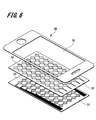
- FIG. 6 shows an example of the configuration of a touch panel including a transparent conductive member having an electrode pattern.
- the touch panel 30 shown in FIG. 6 is a projected capacitive touch panel.
- the touch panel 30 includes a first transparent conductive member 33 patterned on one main surface of the first transparent substrate 31 and a second transparent conductive pattern formed on one main surface of the second transparent substrate 32.
- the members 34 are arranged in this order.
- the upper portions of the second transparent substrate 32 and the second transparent conductive member 34 are covered with the front plate 35.
- Each of the first transparent conductive member 33 and the second transparent conductive member 34 has a desired metal layer pattern according to the conductive region and the non-conductive region shown in the first and second embodiments described above.
- a conductive member can be applied.
- a touch panel can be comprised by laminating
- a transparent substrate (11) As a transparent substrate (11), a polyethylene terephthalate (abbreviation: CHC-PET, manufactured by Kimoto Co.) film on which a double-sided hard coat was formed was prepared. Then, on this CHC-PET film, the first dielectric layer (12) (ZnS-ITO) / metal layer (13) (Ag) / second dielectric layer (14) (by a vapor deposition method according to the following method) ZnS-ITO) were laminated in this order. Then, each formed layer was patterned by the following method, and a transparent conductive member of sample 101 having the same pattern as the wiring shown in FIG. The thickness of each layer is J. A. Woollam Co. Inc. The measurement was made with a VB-250 VASE ellipsometer manufactured by the manufacturer.
- CHC-PET polyethylene terephthalate
- first dielectric layer ZnS-ITO
- a vacuum deposition apparatus a BMC-800T deposition apparatus manufactured by SYNCHRON Co., Ltd. was used. ZnS was loaded on the first resistance heating boat (22) made of molybdenum, and ITO was loaded on the second resistance heating boat (23) made of molybdenum. . Then, after reducing the vacuum tank to 1 ⁇ 10 ⁇ 4 Pa, the first resistance heating boat (22) and the second resistance heating boat (23) are energized and heated, and the current heating conditions of both resistance heating boats are appropriately set.
- the CHC-PET film on which the first dielectric layer (12) is formed is fixed to a vacuum vapor deposition apparatus similar to the above, Ag is loaded into a resistance heating boat (25) made of molybdenum, and the vacuum chamber is set to 1 The pressure was reduced to 10-4 Pa. Then, the resistance heating boat (25) was energized and heated, and was vacuum-deposited on the first dielectric layer under the condition that the formation time was 6 seconds, thereby forming a metal layer (13) having a layer thickness of 7.7 nm. The formation speed at this time was 2.7 nm / second as a result of measurement by the following method.
- the second dielectric layer having a layer thickness of 44 nm is prepared by co-evaporation under the conditions that the volume ratio of ZnS and ITO is 99: 1 and the formation speed is 0.37 nm / second and the formation time is 120 seconds. (14) was formed.
- the volume ratio of ZnS and SiO 2 is 99: 1 in the first resistance heating boat (22, 27).
- the second resistance heating boat (23, 28) was charged with ITO, and the formation rate was 4.3 nm / min under the condition that the volume ratio of ZnS—SiO 2 and ITO was 99: 1. Second, formation time was 10 seconds.
- the first dielectric layer (12) ZnS—SiO 2 —ITO
- metal layer (13) Al
- second dielectric layer (14 ) A transparent conductive member of Sample 105 having a layer structure of (ZnS—SiO 2 —ITO) was prepared.
- Sample 108 was prepared in the same manner as in the preparation of the transparent conductive member of Sample 102 described above, except that ZnS constituting the first dielectric layer (12) and the second dielectric layer (14) was changed to GZO. A transparent conductive member was prepared.
- Sample 109 was prepared in the same manner as in the preparation of the transparent conductive member of Sample 102 described above, except that ZnS constituting the first dielectric layer (12) and the second dielectric layer (14) was changed to ZnO. A transparent conductive member was prepared.
- the first dielectric layer (excluding that the PC200 mixed with 1% of ITO fine particles was formed to 40 nm was formed.
- transparent conductive member of sample 113 The material used to fabricate the first dielectric layer (12) and the second dielectric layer (14) was changed from PC200 to XJA-0291C (titanium oxide particle-dispersed UV curable resin composition, Pernox Corporation).
- a transparent conductive member of Sample 113 was prepared in the same manner as the transparent conductive member of Sample 111 described above, except that after drying, ultraviolet light having an illuminance of 150 mW and a light amount of 100 mJ was irradiated for 5 seconds.
- Sample 115 was prepared in the same manner as in the preparation of the transparent conductive member of Sample 102 described above, except that ITO contained in the first dielectric layer (12) and the second dielectric layer (14) was changed to ATO. A transparent conductive member was prepared.
- Sample 116 was prepared in the same manner as in the preparation of the transparent conductive member of Sample 106 described above except that ITO contained in the first dielectric layer (12) and the second dielectric layer (14) was changed to ATO. A transparent conductive member was prepared.
- Sample 117 is manufactured in the same manner as in the production of the transparent conductive member of Sample 111 described above, except that ITO contained in the first dielectric layer (12) and the second dielectric layer (14) is changed to ATO. A transparent conductive member was prepared.
- the first dielectric layer (12) (ZnS-ITO) / metal layer (13) (Ag) / second dielectric layer (14) on the transparent substrate (11) (CHC-PET film) by the following sputtering method (ZnS-ITO) was laminated in order.
- first dielectric layer (ZnS)) Using a magnetron sputtering apparatus manufactured by Osaka Vacuum Co., Ar: 20 sccm, O 2 : 0 sccm, sputtering pressure 0.1 Pa, room temperature, target side power 150 W, formation rate 0.3. Under the condition of nm / second, a ZnS target and an ITO target were juxtaposed in a volume ratio of 85:15 and RF sputtering was performed to form a first dielectric layer (12) having a layer thickness of 28 nm. The target-substrate distance was 90 mm.
- the first dielectric layer (12) and the second dielectric layer (14) are made of only ZnS and do not contain ITO, except that the first dielectric layer (12) ), A metal layer (13), and a second dielectric layer (14). Then, the formed first dielectric layer (12), metal layer (13), and second dielectric layer (14) were patterned by the following method.
- the first dielectric layer (12), the metal layer (13), and the second dielectric layer (14) were subjected to ultrasonic cleaning treatment.
- An ultrasonic cleaning treatment was performed at 25 ° C. for 4 minutes using a detergent “Clean 30-30 (10%)” manufactured by Kao Corporation as a cleaning solution.
- a detergent “Clean 30-30 (10%)” manufactured by Kao Corporation as a cleaning solution.
- ultrasonic washing with pure water at 25 ° C. was performed twice for 4 minutes.
- OFPR-800LB manufactured by Tokyo Ohka Kogyo Co., Ltd. is applied as a resist on the cleaned first dielectric layer (12), metal layer (13), and second dielectric layer (14) by spin coating. Then, application and drying were performed at 2000 rpm for 30 seconds to form a resist layer having a thickness of 1 ⁇ m.
- ultraviolet rays were irradiated through a mask under conditions of 60 mJ, and developed using a developer for positive photoresist “Tokuso SD-1” (tetramethylammonium hydroxide) manufactured by Tokuyama Corporation as a developer. .
- Yamaso SD-1 tetramethylammonium hydroxide
- ITO series manufactured by Kanto Chemical Co., Ltd. is used as an etchant, and the non-conductive region (17) where the transparent substrate is exposed, the first dielectric layer (12), the metal layer (13), and the second An electrode pattern composed of a current-carrying region (16) in which the dielectric layer (14) remained was formed.
- the width of the line-shaped non-conducting region (17) was 16 ⁇ m.
- the remaining resist layer was peeled off using acetone to form an electrode pattern having wiring.
- the transparent conductive member of the sample 121 was formed in the same manner as the sample 101 except that the first dielectric layer (12) and the second dielectric layer (14) were formed only of ZnS and did not contain ITO. Produced.
- permeability was measured in accordance with the following method.
- the transparent conductive member and a non-alkali glass substrate (EAGLE XG (thickness 7 mm ⁇ length 30 mm ⁇ width 30 mm) manufactured by Corning) were bonded together, and the average in the wavelength range of 400 to 1200 nm from the alkali-free glass substrate side.
- the transmittance (%) was measured.
- measurement light for example, light having a wavelength of 450 nm to 1200 nm
- the light transmittance was measured at U4100.
- the absorptance (%) of the laser light wavelength 1064 nm of each sample was measured.
- the transparent conductive members of Samples 101 to 119 having infrared absorbing compounds in the first dielectric layer and the second dielectric layer have absorption in the 1064 nm laser. Yes. For this reason, it can be seen that desired etching is possible with the laser, and the transmittance, resistance value, and haze are good.
- the transparent conductive members of the sample 120 and the sample 121 that do not have the infrared absorbing compound in the first dielectric layer and the second dielectric layer do not have absorption in the 1064 nm laser.
- the transparent conductive member of the sample 121 was not satisfactorily laser-etched and could not be measured for each evaluation after the etching. Further, even in the sample 120 subjected to wet etching, the etching was not performed well, and each evaluation after the etching could not be measured.
Landscapes
- Engineering & Computer Science (AREA)
- General Engineering & Computer Science (AREA)
- Theoretical Computer Science (AREA)
- Human Computer Interaction (AREA)
- Physics & Mathematics (AREA)
- General Physics & Mathematics (AREA)
- Laminated Bodies (AREA)
- Non-Insulated Conductors (AREA)
- Manufacturing Of Electric Cables (AREA)
Abstract
Selon l'invention, un élément conducteur transparent est conçu de manière à être pourvu d'une première couche diélectrique, d'une seconde couche diélectrique, et d'une couche métallique qui est formée entre la première couche diélectrique et la seconde couche diélectrique. Cet élément conducteur transparent est également conçu de manière que la première couche diélectrique et la deuxième couche diélectrique contiennent un composé absorbant les infrarouges.
Priority Applications (1)
| Application Number | Priority Date | Filing Date | Title |
|---|---|---|---|
| JP2016511467A JPWO2015151677A1 (ja) | 2014-03-31 | 2015-02-27 | 透明導電部材、及び、透明導電部材の製造方法 |
Applications Claiming Priority (2)
| Application Number | Priority Date | Filing Date | Title |
|---|---|---|---|
| JP2014072204 | 2014-03-31 | ||
| JP2014-072204 | 2014-03-31 |
Publications (1)
| Publication Number | Publication Date |
|---|---|
| WO2015151677A1 true WO2015151677A1 (fr) | 2015-10-08 |
Family
ID=54240010
Family Applications (1)
| Application Number | Title | Priority Date | Filing Date |
|---|---|---|---|
| PCT/JP2015/055821 Ceased WO2015151677A1 (fr) | 2014-03-31 | 2015-02-27 | Film conducteur transparent et procédé de fabrication d'un élément conducteur transparent |
Country Status (2)
| Country | Link |
|---|---|
| JP (1) | JPWO2015151677A1 (fr) |
| WO (1) | WO2015151677A1 (fr) |
Cited By (1)
| Publication number | Priority date | Publication date | Assignee | Title |
|---|---|---|---|---|
| CN114600202A (zh) * | 2020-09-09 | 2022-06-07 | 株式会社东芝 | 透明电极、透明电极的制造方法和电子器件 |
Citations (6)
| Publication number | Priority date | Publication date | Assignee | Title |
|---|---|---|---|---|
| JPH04310550A (ja) * | 1991-04-10 | 1992-11-02 | Asahi Glass Co Ltd | 積層ガラス構造 |
| JPH1170610A (ja) * | 1996-07-26 | 1999-03-16 | Asahi Glass Co Ltd | 透明導電膜、および透明電極の形成方法 |
| JP2004296140A (ja) * | 2003-03-25 | 2004-10-21 | Mitsui Chemicals Inc | 透明導電性薄膜積層体 |
| JP2004342375A (ja) * | 2003-05-13 | 2004-12-02 | Mitsui Chemicals Inc | 発光体 |
| JP2010157497A (ja) * | 2008-12-02 | 2010-07-15 | Geomatec Co Ltd | 透明導電膜付き基板とその製造方法 |
| JP2013008099A (ja) * | 2011-06-22 | 2013-01-10 | Reiko Co Ltd | 光学調整フィルム、並びにそれを使用して得る透明導電フィルム、透明導電積層体、及びタッチパネル |
-
2015
- 2015-02-27 JP JP2016511467A patent/JPWO2015151677A1/ja active Pending
- 2015-02-27 WO PCT/JP2015/055821 patent/WO2015151677A1/fr not_active Ceased
Patent Citations (6)
| Publication number | Priority date | Publication date | Assignee | Title |
|---|---|---|---|---|
| JPH04310550A (ja) * | 1991-04-10 | 1992-11-02 | Asahi Glass Co Ltd | 積層ガラス構造 |
| JPH1170610A (ja) * | 1996-07-26 | 1999-03-16 | Asahi Glass Co Ltd | 透明導電膜、および透明電極の形成方法 |
| JP2004296140A (ja) * | 2003-03-25 | 2004-10-21 | Mitsui Chemicals Inc | 透明導電性薄膜積層体 |
| JP2004342375A (ja) * | 2003-05-13 | 2004-12-02 | Mitsui Chemicals Inc | 発光体 |
| JP2010157497A (ja) * | 2008-12-02 | 2010-07-15 | Geomatec Co Ltd | 透明導電膜付き基板とその製造方法 |
| JP2013008099A (ja) * | 2011-06-22 | 2013-01-10 | Reiko Co Ltd | 光学調整フィルム、並びにそれを使用して得る透明導電フィルム、透明導電積層体、及びタッチパネル |
Cited By (1)
| Publication number | Priority date | Publication date | Assignee | Title |
|---|---|---|---|---|
| CN114600202A (zh) * | 2020-09-09 | 2022-06-07 | 株式会社东芝 | 透明电极、透明电极的制造方法和电子器件 |
Also Published As
| Publication number | Publication date |
|---|---|
| JPWO2015151677A1 (ja) | 2017-04-13 |
Similar Documents
| Publication | Publication Date | Title |
|---|---|---|
| JP6314463B2 (ja) | 透明導電体 | |
| JP6292225B2 (ja) | 透明導電体 | |
| JP6319302B2 (ja) | 透明導電体及びその製造方法 | |
| JP2016081318A (ja) | 透明導電体及びタッチパネル | |
| WO2014064939A1 (fr) | Conducteur transparent | |
| WO2015068738A1 (fr) | Corps conducteur transparent | |
| JP6344095B2 (ja) | 透明導電体及びタッチパネル | |
| JP6206262B2 (ja) | 透明導電体、その製造方法及び導電性ペースト | |
| WO2015025525A1 (fr) | Corps conducteur transparent | |
| JPWO2015194320A1 (ja) | 透明導電体及びタッチパネル | |
| WO2015151677A1 (fr) | Film conducteur transparent et procédé de fabrication d'un élément conducteur transparent | |
| JP2016152182A (ja) | 透明導電膜、透明導電膜の製造方法、及び、電子機器 | |
| JP6627769B2 (ja) | 透明導電体及びこれを含むタッチパネル | |
| WO2015087895A1 (fr) | Corps conducteur transparent | |
| JP2016091071A (ja) | 透明導電性フィルムとその製造方法 | |
| JP6493225B2 (ja) | 透明導電性フィルム | |
| JP2016177940A (ja) | 透明導電体の製造方法 | |
| JP2016146052A (ja) | 透明導電体及びこれを含むタッチパネル | |
| WO2015125677A1 (fr) | Conducteur transparent | |
| JP6586738B2 (ja) | 透明導電部材、及び、透明導電部材の製造方法 | |
| JP2016169420A (ja) | 透明導電部材の製造装置、及び、透明導電部材の製造方法 | |
| WO2015011928A1 (fr) | Procédé de production d'un corps conducteur transparent | |
| WO2015107968A1 (fr) | Procédé de fabrication de conducteur transparent et conducteur transparent | |
| WO2015053371A1 (fr) | Conducteur transparent | |
| WO2015190227A1 (fr) | Procédé de fabrication de conducteur transparent |
Legal Events
| Date | Code | Title | Description |
|---|---|---|---|
| 121 | Ep: the epo has been informed by wipo that ep was designated in this application |
Ref document number: 15773137 Country of ref document: EP Kind code of ref document: A1 |
|
| ENP | Entry into the national phase |
Ref document number: 2016511467 Country of ref document: JP Kind code of ref document: A |
|
| NENP | Non-entry into the national phase | ||
| 122 | Ep: pct application non-entry in european phase |
Ref document number: 15773137 Country of ref document: EP Kind code of ref document: A1 |