WO2015178019A1 - 光電気化学反応装置 - Google Patents
光電気化学反応装置 Download PDFInfo
- Publication number
- WO2015178019A1 WO2015178019A1 PCT/JP2015/002527 JP2015002527W WO2015178019A1 WO 2015178019 A1 WO2015178019 A1 WO 2015178019A1 JP 2015002527 W JP2015002527 W JP 2015002527W WO 2015178019 A1 WO2015178019 A1 WO 2015178019A1
- Authority
- WO
- WIPO (PCT)
- Prior art keywords
- layer
- electrode layer
- reduction
- potential
- oxidation
- Prior art date
- Legal status (The legal status is an assumption and is not a legal conclusion. Google has not performed a legal analysis and makes no representation as to the accuracy of the status listed.)
- Ceased
Links
Images







Classifications
-
- C—CHEMISTRY; METALLURGY
- C25—ELECTROLYTIC OR ELECTROPHORETIC PROCESSES; APPARATUS THEREFOR
- C25B—ELECTROLYTIC OR ELECTROPHORETIC PROCESSES FOR THE PRODUCTION OF COMPOUNDS OR NON-METALS; APPARATUS THEREFOR
- C25B1/00—Electrolytic production of inorganic compounds or non-metals
- C25B1/50—Processes
- C25B1/55—Photoelectrolysis
-
- C—CHEMISTRY; METALLURGY
- C25—ELECTROLYTIC OR ELECTROPHORETIC PROCESSES; APPARATUS THEREFOR
- C25B—ELECTROLYTIC OR ELECTROPHORETIC PROCESSES FOR THE PRODUCTION OF COMPOUNDS OR NON-METALS; APPARATUS THEREFOR
- C25B1/00—Electrolytic production of inorganic compounds or non-metals
- C25B1/01—Products
- C25B1/02—Hydrogen or oxygen
- C25B1/04—Hydrogen or oxygen by electrolysis of water
-
- C—CHEMISTRY; METALLURGY
- C25—ELECTROLYTIC OR ELECTROPHORETIC PROCESSES; APPARATUS THEREFOR
- C25B—ELECTROLYTIC OR ELECTROPHORETIC PROCESSES FOR THE PRODUCTION OF COMPOUNDS OR NON-METALS; APPARATUS THEREFOR
- C25B11/00—Electrodes; Manufacture thereof not otherwise provided for
- C25B11/02—Electrodes; Manufacture thereof not otherwise provided for characterised by shape or form
- C25B11/03—Electrodes; Manufacture thereof not otherwise provided for characterised by shape or form perforated or foraminous
-
- C—CHEMISTRY; METALLURGY
- C25—ELECTROLYTIC OR ELECTROPHORETIC PROCESSES; APPARATUS THEREFOR
- C25B—ELECTROLYTIC OR ELECTROPHORETIC PROCESSES FOR THE PRODUCTION OF COMPOUNDS OR NON-METALS; APPARATUS THEREFOR
- C25B11/00—Electrodes; Manufacture thereof not otherwise provided for
- C25B11/02—Electrodes; Manufacture thereof not otherwise provided for characterised by shape or form
- C25B11/03—Electrodes; Manufacture thereof not otherwise provided for characterised by shape or form perforated or foraminous
- C25B11/031—Porous electrodes
-
- C—CHEMISTRY; METALLURGY
- C25—ELECTROLYTIC OR ELECTROPHORETIC PROCESSES; APPARATUS THEREFOR
- C25B—ELECTROLYTIC OR ELECTROPHORETIC PROCESSES FOR THE PRODUCTION OF COMPOUNDS OR NON-METALS; APPARATUS THEREFOR
- C25B3/00—Electrolytic production of organic compounds
- C25B3/01—Products
- C25B3/07—Oxygen containing compounds
-
- C—CHEMISTRY; METALLURGY
- C25—ELECTROLYTIC OR ELECTROPHORETIC PROCESSES; APPARATUS THEREFOR
- C25B—ELECTROLYTIC OR ELECTROPHORETIC PROCESSES FOR THE PRODUCTION OF COMPOUNDS OR NON-METALS; APPARATUS THEREFOR
- C25B3/00—Electrolytic production of organic compounds
- C25B3/20—Processes
- C25B3/25—Reduction
-
- C—CHEMISTRY; METALLURGY
- C25—ELECTROLYTIC OR ELECTROPHORETIC PROCESSES; APPARATUS THEREFOR
- C25B—ELECTROLYTIC OR ELECTROPHORETIC PROCESSES FOR THE PRODUCTION OF COMPOUNDS OR NON-METALS; APPARATUS THEREFOR
- C25B3/00—Electrolytic production of organic compounds
- C25B3/20—Processes
- C25B3/25—Reduction
- C25B3/26—Reduction of carbon dioxide
-
- H—ELECTRICITY
- H10—SEMICONDUCTOR DEVICES; ELECTRIC SOLID-STATE DEVICES NOT OTHERWISE PROVIDED FOR
- H10F—INORGANIC SEMICONDUCTOR DEVICES SENSITIVE TO INFRARED RADIATION, LIGHT, ELECTROMAGNETIC RADIATION OF SHORTER WAVELENGTH OR CORPUSCULAR RADIATION
- H10F10/00—Individual photovoltaic cells, e.g. solar cells
- H10F10/10—Individual photovoltaic cells, e.g. solar cells having potential barriers
- H10F10/19—Photovoltaic cells having multiple potential barriers of different types, e.g. tandem cells having both PN and PIN junctions
-
- H—ELECTRICITY
- H10—SEMICONDUCTOR DEVICES; ELECTRIC SOLID-STATE DEVICES NOT OTHERWISE PROVIDED FOR
- H10F—INORGANIC SEMICONDUCTOR DEVICES SENSITIVE TO INFRARED RADIATION, LIGHT, ELECTROMAGNETIC RADIATION OF SHORTER WAVELENGTH OR CORPUSCULAR RADIATION
- H10F77/00—Constructional details of devices covered by this subclass
- H10F77/40—Optical elements or arrangements
- H10F77/42—Optical elements or arrangements directly associated or integrated with photovoltaic cells, e.g. light-reflecting means or light-concentrating means
- H10F77/48—Back surface reflectors [BSR]
-
- B—PERFORMING OPERATIONS; TRANSPORTING
- B01—PHYSICAL OR CHEMICAL PROCESSES OR APPARATUS IN GENERAL
- B01J—CHEMICAL OR PHYSICAL PROCESSES, e.g. CATALYSIS OR COLLOID CHEMISTRY; THEIR RELEVANT APPARATUS
- B01J35/00—Catalysts, in general, characterised by their form or physical properties
- B01J35/30—Catalysts, in general, characterised by their form or physical properties characterised by their physical properties
- B01J35/33—Electric or magnetic properties
-
- H—ELECTRICITY
- H01—ELECTRIC ELEMENTS
- H01G—CAPACITORS; CAPACITORS, RECTIFIERS, DETECTORS, SWITCHING DEVICES, LIGHT-SENSITIVE OR TEMPERATURE-SENSITIVE DEVICES OF THE ELECTROLYTIC TYPE
- H01G9/00—Electrolytic capacitors, rectifiers, detectors, switching devices, light-sensitive or temperature-sensitive devices; Processes of their manufacture
- H01G9/20—Light-sensitive devices
- H01G9/2004—Light-sensitive devices characterised by the electrolyte, e.g. comprising an organic electrolyte
- H01G9/2013—Light-sensitive devices characterised by the electrolyte, e.g. comprising an organic electrolyte the electrolyte comprising ionic liquids, e.g. alkyl imidazolium iodide
-
- Y—GENERAL TAGGING OF NEW TECHNOLOGICAL DEVELOPMENTS; GENERAL TAGGING OF CROSS-SECTIONAL TECHNOLOGIES SPANNING OVER SEVERAL SECTIONS OF THE IPC; TECHNICAL SUBJECTS COVERED BY FORMER USPC CROSS-REFERENCE ART COLLECTIONS [XRACs] AND DIGESTS
- Y02—TECHNOLOGIES OR APPLICATIONS FOR MITIGATION OR ADAPTATION AGAINST CLIMATE CHANGE
- Y02E—REDUCTION OF GREENHOUSE GAS [GHG] EMISSIONS, RELATED TO ENERGY GENERATION, TRANSMISSION OR DISTRIBUTION
- Y02E10/00—Energy generation through renewable energy sources
- Y02E10/50—Photovoltaic [PV] energy
- Y02E10/52—PV systems with concentrators
-
- Y—GENERAL TAGGING OF NEW TECHNOLOGICAL DEVELOPMENTS; GENERAL TAGGING OF CROSS-SECTIONAL TECHNOLOGIES SPANNING OVER SEVERAL SECTIONS OF THE IPC; TECHNICAL SUBJECTS COVERED BY FORMER USPC CROSS-REFERENCE ART COLLECTIONS [XRACs] AND DIGESTS
- Y02—TECHNOLOGIES OR APPLICATIONS FOR MITIGATION OR ADAPTATION AGAINST CLIMATE CHANGE
- Y02E—REDUCTION OF GREENHOUSE GAS [GHG] EMISSIONS, RELATED TO ENERGY GENERATION, TRANSMISSION OR DISTRIBUTION
- Y02E60/00—Enabling technologies; Technologies with a potential or indirect contribution to GHG emissions mitigation
- Y02E60/30—Hydrogen technology
- Y02E60/36—Hydrogen production from non-carbon containing sources, e.g. by water electrolysis
-
- Y—GENERAL TAGGING OF NEW TECHNOLOGICAL DEVELOPMENTS; GENERAL TAGGING OF CROSS-SECTIONAL TECHNOLOGIES SPANNING OVER SEVERAL SECTIONS OF THE IPC; TECHNICAL SUBJECTS COVERED BY FORMER USPC CROSS-REFERENCE ART COLLECTIONS [XRACs] AND DIGESTS
- Y02—TECHNOLOGIES OR APPLICATIONS FOR MITIGATION OR ADAPTATION AGAINST CLIMATE CHANGE
- Y02P—CLIMATE CHANGE MITIGATION TECHNOLOGIES IN THE PRODUCTION OR PROCESSING OF GOODS
- Y02P20/00—Technologies relating to chemical industry
- Y02P20/10—Process efficiency
- Y02P20/133—Renewable energy sources, e.g. sunlight
Definitions
- the invention of the embodiment relates to a photoelectrochemical reaction apparatus.
- a photoelectrochemical reaction apparatus for converting sunlight into a chemical substance electrochemically for example, it has an electrode having a reduction catalyst for reducing carbon dioxide (CO 2 ) and an oxidation catalyst for oxidizing water (H 2 O).
- CO 2 carbon dioxide
- H 2 O oxidizing water
- a two-electrode type apparatus that includes electrodes and immerses these electrodes in water in which CO 2 is dissolved. At this time, each electrode is electrically connected via an electric wire or the like.
- H 2 O is oxidized by light energy to obtain oxygen (1 / 2O 2 ) and a potential is obtained.
- CO 2 is reduced by generating a potential from an electrode that causes an oxidation reaction to produce formic acid (HCOOH) or the like.
- HCOOH formic acid
- the conversion efficiency from sunlight to chemical energy is as low as about 0.04%.
- a photoelectrochemical reaction device for example, a device that performs photoelectric conversion using GaN, oxidizes water on the surface, and reduces CO 2 with an electrically connected copper plate is known. However, the conversion efficiency is as low as 0.2%.
- JP 2011-094194 A Japanese Patent Laid-Open No. 10-290017
- the problem to be solved by the invention of the embodiment is to increase the conversion efficiency from light to a carbon compound.
- the photoelectrochemical reaction device of the embodiment includes an electrolytic solution, an oxidation electrode layer immersed in the electrolytic solution, a reduction electrode layer immersed in the electrolytic solution, and a first surface electrically connected to the oxidation electrode layer. And a second surface that faces the first surface and is electrically connected to the reduction electrode layer, and performs charge separation by the energy of light irradiated on the first surface or the second surface.
- a photoelectrochemical reaction device comprising an electromotive force layer. At least one of the oxidation electrode layer and the reduction electrode layer has a porous structure including pores.
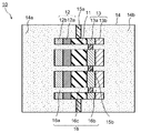
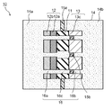
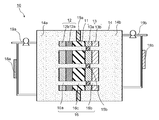
- FIG. 1 is a schematic diagram showing a configuration example of a photoelectrochemical reaction apparatus.
- a photoelectrochemical reaction device 10 shown in FIG. 1 includes a photovoltaic layer 11, an oxidation electrode layer 12, a reduction electrode layer 13, an electrolytic solution 14, an ion exchange membrane 15a, and an ion exchange membrane 15b. To do. Further, the photoelectrochemical reaction device 10 has a through hole 16.
- the through hole 16 includes a through hole 16 a that penetrates the oxidation electrode layer 12, a through hole 16 b that penetrates the reduction electrode layer 13, and a through hole 16 c that penetrates the photovoltaic layer 11.
- the through holes 16a to 16c are provided so as to communicate with each other. The diameters of the through holes 16a to the through holes 16c may be different from each other. Further, the through holes 16a to 16c are not necessarily provided. Furthermore, the through holes 16a to 16c do not have to communicate with each other.
- the photovoltaic layer 11 has a function of performing charge separation by the energy of light such as irradiated sunlight.
- the holes generated by the charge separation move to the oxidation electrode layer 12 side, and the electrons move to the reduction electrode layer 13 side. Thereby, the photovoltaic layer 11 can generate an electromotive force.
- the photovoltaic layer 11 has a first surface and a second surface that face each other.
- a pn junction type or pin junction type photoelectric conversion layer can be used as the photovoltaic layer 11 may be formed by stacking a plurality of photoelectric conversion layers.
- the through-hole 16c of the photovoltaic layer 11 is formed by removing a part of the photovoltaic layer 11 by etching or the like, for example.
- the through hole 16c may be formed by a plurality of opening processes.
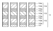
- FIG. 2 is a schematic diagram showing a structural example of the photovoltaic layer 11.
- the photovoltaic layer 11 shown in FIG. 2 includes a reflective layer 111, a photoelectric conversion layer 112, a photoelectric conversion layer 113, and a photoelectric conversion layer 114. Note that the reflective layer 111 is not necessarily provided.
- the reflective layer 111 is made of a material having light reflectivity.
- a distributed Bragg reflective layer made of a stacked layer of a metal layer or a semiconductor layer can be cited.
- the reflective layer 111 examples include a layer of a metal such as Ag, Au, Al, or Cu, or an alloy including at least one of these metals.
- the reflective layer 111 may be a stack of a first reflective layer and a second reflective layer.
- the first reflective layer has light reflectivity and conductivity
- the second reflective layer has translucency.
- the first reflective layer the above metal material or alloy can be used.
- the second reflective layer is provided for adjusting the optical distance and enhancing the light reflectivity.
- the second reflective layer is preferably formed of a material that has optical transparency and can make ohmic contact with the n-type semiconductor layer.
- the second reflecting layer examples include indium tin oxide (Indium Tin Oxide: ITO), zinc oxide (ZnO), tin oxide containing fluorine (Fluorine-doped Tin Oxide: FTO), and zinc oxide containing aluminum (Aluminum- Examples thereof include a layer of a light-transmitting metal oxide such as doped Zinc Oxide (AZO) and tin oxide containing antimony (Antimony-doped Tin Oxide: ATO).
- ITO Indium Tin Oxide
- ZnO zinc oxide
- FTO tin oxide containing fluorine
- FTO tin oxide containing aluminum
- Al zinc oxide containing aluminum
- aluminum- Examples thereof include a layer of a light-transmitting metal oxide such as doped Zinc Oxide (AZO) and tin oxide containing antimony (Antimony-doped Tin Oxide: ATO).
- the photoelectric conversion layer 112 is provided on the reflective layer 111.
- the photoelectric conversion layer 112 includes an n-type semiconductor layer 112a made of n-type amorphous silicon (a-Si) and an i-type semiconductor layer made of intrinsic amorphous silicon germanium (a-SiGe), which are sequentially stacked from the lower side. 112b and a p-type semiconductor layer 112c made of p-type microcrystalline silicon (uc-Si).
- the i-type semiconductor layer 112b is a layer that absorbs light in a short wavelength region of about 400 nm. Therefore, in the photoelectric conversion layer 112, charge separation occurs due to light energy in a short wavelength region.
- the photoelectric conversion layer 113 is provided on the photoelectric conversion layer 112.
- the photoelectric conversion layer 113 includes an n-type semiconductor layer 113a made of n-type a-Si, an i-type semiconductor layer 113b made of intrinsic a-SiGe, and a p-type made of p-type uc-Si.
- a type semiconductor layer 113c is provided.
- the i-type semiconductor layer 113b is a layer that absorbs light in the intermediate wavelength region of about 600 nm. Therefore, in the photoelectric conversion layer 113, charge separation occurs due to light energy in the intermediate wavelength region.
- the photoelectric conversion layer 114 is provided on the photoelectric conversion layer 113.
- the photoelectric conversion layer 114 includes an n-type semiconductor layer 114a made of n-type a-Si, an i-type semiconductor layer 114b made of intrinsic a-Si, and a p-type uc-Si stacked in order from the lower side.
- a p-type semiconductor layer 114c is provided.
- the i-type semiconductor layer 114b is a layer that absorbs light in a long wavelength region of about 700 nm. Therefore, in the photoelectric conversion layer 114, charge separation occurs due to light energy in the long wavelength region.
- the p-type semiconductor layer or the n-type semiconductor layer can be formed, for example, by adding an element serving as a donor or an acceptor to a semiconductor material.
- a semiconductor layer containing silicon, germanium, or the like is used as the semiconductor layer.
- the present invention is not limited to this, and for example, a compound semiconductor layer or the like can be used.
- the compound semiconductor layer for example, a semiconductor layer containing GaAs, GaInP, AlGaInP, CdTe, CuInGaSe, or the like can be used.
- a semiconductor layer such as TiO 2 or WO 3 may be used.
- each semiconductor layer may be single crystal, polycrystalline, or amorphous.
- a zinc oxide layer may be provided on the photoelectric conversion layer.
- the photovoltaic layer 11 shown in FIG. 2 can absorb light of a wide wavelength of sunlight by stacking the photoelectric conversion layer 112 to the photoelectric conversion layer 114, and more solar energy can be absorbed. It can be used efficiently. At this time, a high voltage can be obtained because the photoelectric conversion layers are connected in series. For example, a plurality of photoelectric conversion layers may be electrically connected in parallel connection. Alternatively, a two-junction type or single-layer type photovoltaic layer may be used.
- the present invention is not limited to this and may have a stack of two or four or more photoelectric conversion layers. . Further, instead of stacking a plurality of photoelectric conversion layers, one photoelectric conversion layer may be used. The above is the description of the structure example of the photovoltaic layer 11 shown in FIG.
- the oxidation electrode layer 12 shown in FIG. 1 is electrically connected to the first surface of the photovoltaic layer 11.
- the oxidation electrode layer 12 has a function of generating hydrogen ions by an oxidation reaction of water.
- the oxidation electrode layer 12 includes a conductive material and an oxidation catalyst.
- the oxidation electrode layer 12 includes a conductive layer 12a including a conductive material and an oxidation catalyst layer 12b including an oxidation catalyst stacked on the conductive layer 12a.
- the oxidation catalyst layer 12b may be in the form of a thin film, a lattice, a particle, or a wire, for example.
- the oxidation electrode layer 12 is made of, for example, a conductive material capable of ohmic contact with the p-type semiconductor layer 114c in the photovoltaic layer 11.
- the conductive material include a material containing at least one of Ag, Au, Al, and Cu.
- a light-transmitting metal oxide such as ITO, ZnO, FTO, AZO, or ATO may be used as the conductive material.
- the oxidized electrode layer 12 may be, for example, a laminate of a metal and a translucent metal oxide, a layer containing a metal and another conductive material, or a layer containing a translucent metal oxide and another conductive material. Good.
- the oxidation electrode layer 12 When light is irradiated to the photovoltaic layer 11 through the oxidation electrode layer 12, the oxidation electrode layer 12 needs to have translucency. At this time, the light transmittance of the oxidation electrode layer 12 is, for example, at least 10% or more, more preferably 30% or more, of the amount of light irradiated to the oxidation electrode layer 12.
- the oxidation catalyst examples include a material that reduces activation energy for oxidizing water, in other words, a material that reduces an overvoltage when oxygen and hydrogen ions are generated by an oxidation reaction of water.
- a material that reduces an overvoltage when oxygen and hydrogen ions are generated by an oxidation reaction of water For example, iridium, platinum, cobalt, a manganese catalyst, etc. are mentioned.
- a binary metal oxide, a ternary metal oxide, a quaternary metal oxide, or the like can be used.
- binary metal oxides include manganese oxide (Mn—O), iridium oxide (Ir—O), nickel oxide (Ni—O), cobalt oxide (Co—O), iron oxide (Fe—O), Examples thereof include tin oxide (Sn—O), indium oxide (In—O), and ruthenium oxide (Ru—O).
- Examples of the ternary metal oxide include Ni—Co—O, La—Co—O, Ni—La—O, and Sr—Fe—O.
- Examples of the quaternary metal oxide include Pb—Ru—Ir—O and La—Sr—Co—O. Note that the present invention is not limited to this, and a metal complex such as a Ru complex or an Fe complex can also be used as an oxidation catalyst. A plurality of materials may be mixed.
- the through hole 16a of the oxidation electrode layer 12 may be formed in the oxidation electrode layer 12 in advance, for example.
- the through-hole 16a can be formed by removing a part of the oxidation electrode layer 12 by etching or the like.
- the through hole 16a may be formed by a plurality of opening processes.
- the reduction electrode layer 13 is electrically connected to the second surface of the photovoltaic layer 11.
- the reduction electrode layer 13 has a function of generating a carbon compound by a reduction reaction of carbon dioxide.
- the carbon compound produced by the reduction reaction varies depending on the type of reduction catalyst.
- CO carbon monoxide
- HCOOH formic acid
- methane CH 4
- methanol CH 3 OH
- ethane C 2 H 6
- ethylene C 2 H 4
- ethanol C 2 H 5 OH
- Formaldehyde HCHO
- acetaldehyde CH 3 CHO
- acetic acid CH 3 COOH
- ethylene glycol HOCH 2 CH 2 OH
- 1-propanol CH 2 CH 2 OH
- isopropanol CHOHCH 3
- the reduction electrode layer 13 includes a conductive material and a reduction catalyst.
- the reduction electrode layer 13 includes a conductive layer 13a including a conductive material and a reduction catalyst layer 13b stacked on the conductive layer 13a and including a reduction catalyst.
- the reduction catalyst layer 13b may be, for example, a thin film shape, a lattice shape, a particle shape, or a wire shape.
- the present invention is not limited to this, and the reduction electrode layer 13 may be formed of a single layer including both the conductive material and the reduction catalyst.
- the reducing electrode layer 13 may be a layer made of a material that can make ohmic contact with the n-type semiconductor layer 112a in the photovoltaic layer 11.
- a metal such as Ag, Au, Al, Pd, Sn, Bi, or Cu, or an alloy material such as SUS including a plurality of the metals can be used.
- the mechanical strength of the photoelectrochemical reaction cell composed of the photovoltaic layer 11, the oxidation electrode layer 12, and the reduction electrode layer 13 can be increased by forming the conductive layer 13 a with the substrate of the above material.
- a light-transmitting metal oxide such as ITO, ZnO, FTO, AZO, or ATO may be used as the conductive material.
- the reduction electrode layer 13 may be, for example, a laminate of a metal and a translucent metal oxide, a layer including a metal and another conductive material, or a layer including a translucent metal oxide and another conductive material. Good.
- a semiconductor substrate such as silicon or germanium, a conductive resin, a conductive ion exchange membrane, or the like may be used as the conductive material.
- a resin material such as an ionomer may be used.
- the reduction catalyst examples include a material that reduces activation energy for reducing carbon dioxide, in other words, a material that reduces an overvoltage when a carbon compound is generated by a reduction reaction of carbon dioxide.
- a metal material or a carbon material can be used.
- the metal material for example, Au, Ag, Cu, Pt, Ni, Zn, or Pd can be used.
- the carbon material for example, carbon, graphene, carbon nanotube (Carbon Nanotube: CNT), fullerene, ketjen black, or the like can be used.
- metal complexes such as Ru complex or Re complex
- a plurality of materials may be mixed.
- the reduction electrode layer 13 has a porous structure including pores for allowing the electrolytic solution 14 to pass therethrough.
- the porous structure is formed by, for example, a method of forming pores by processing a material having no pores, a method using a porous material, or the like.
- Examples of materials applicable to the reduction electrode layer 13 having a porous structure include, in addition to the above materials, carbon black such as Ketjen Black and Vulcan XC-72, activated carbon, and metal fine powder.
- a material applicable to the reduction electrode layer 13 having the porous structure may be used for the conductive layer 13a.
- the porous structure preferably has a pore distribution of 5 nm to 100 nm.
- the catalytic activity can be enhanced.
- the porous structure preferably has a plurality of pore distribution peaks. Thereby, an increase in surface area, an improvement in diffusibility of ions and reactants, and high conductivity can all be realized simultaneously.
- a reduction catalyst layer 13b including metal or alloy fine particles (particulate reduction catalyst) applicable to the above-described reduction catalyst of 100 nm or less is laminated on the conductive layer 13a having a pore distribution of 5 micrometers to 10 micrometers. May be.
- the fine particles may also have a porous structure, but may not necessarily have a porous structure from the relationship between conductivity and reaction sites and substance diffusion. Further, the fine particles may be carried on another material. By doing so, the conductivity of the catalyst layer and the gas diffusibility, the contact probability between the catalyst particles and the gaseous reaction molecules and ions are improved, and the reaction efficiency is improved.
- the diameter of the fine particles is preferably smaller.
- the fine particles having a particle size of 10 nm or less are more than 50%, preferably 70% or more.
- the average particle diameter R and the standard deviation ⁇ satisfy the relationship of R + 2 ⁇ ⁇ 10 nm.
- ketjen black particles (hereinafter also simply referred to as ketjen black particles) carrying gold particles are not particularly limited to Nafion (registered trademark), but preferably 1 :
- a paste is prepared by mixing at about 3 (mass ratio).
- the paste is applied to carbon paper.
- the carbon paper and the SUS substrate are bonded with the conductive carbon paste sandwiched so that the SUS substrate faces the surface on which the paste is applied on the carbon paper, and the exposed surface of the SUS substrate and the electrode connection portion are bonded with an epoxy resin.
- An evaluation sample is produced by sealing.
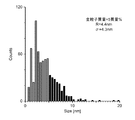
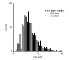
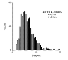
- FIG. 11 to FIG. 14 are diagrams showing the particle size distribution of 300 gold particles in the evaluation sample.
- FIG. 11 shows a particle size distribution of an evaluation sample in which the gold particle mass% obtained by (gold particle mass / (gold particle mass + Ketjen black mass)) ⁇ 100 is 1 mass%
- FIG. 12 shows the gold particle mass.
- % Is the particle size distribution of the evaluation sample with 5% by mass
- FIG. 13 is the particle size distribution of the evaluation sample with 19% by mass of the gold particles
- FIG. 14 is 24% by mass of the gold particles.
- % Is the particle size distribution of the evaluation sample.
- the average particle diameter R and standard deviation ⁇ of gold particles in each evaluation sample are shown in FIGS.
- the gold particles are specified by, for example, an electron microscope or X-ray crystal structure analysis.
- the particle diameter of the gold particles is measured using a measuring method according to, for example, JISH7803 to JISH7805.
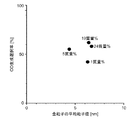
- FIG. 15 is a graph showing the relationship between the average particle size of gold particles and the production selectivity of carbon monoxide.
- the carbon monoxide production selectivity exceeds 50%.
- the carbon monoxide production selectivity is less than 50%. It can also be seen that the carbon monoxide production selectivity may exceed 50% even if the gold particle mass% is low. Furthermore, it can be seen that there is no significant correlation between the average particle diameter of gold particles and the production selectivity of carbon monoxide.
- FIG. 16 is a graph showing the relationship between the proportion of gold particles having a particle size of 5 nm or less and the carbon monoxide production selectivity.
- the curve in FIG. 16 is an approximate curve based on the value of each evaluation sample. As shown in FIG. 16, in the evaluation sample in which the proportion of gold particles having a particle size of 5 nm or less exceeds 25% of the total number of fine particles, it can be seen that the carbon monoxide production selectivity exceeds 50%.
- the ratio of the active surface increases exponentially as the particle size decreases.
- a particle size of 5 nm or less can be said to have a sufficient active surface.
- gold particles having a particle size of 5 nm or less are contained by 25% or more of the total gold particles. .
- Non-Patent Document 2 the average particle diameter of gold particles is 4 nm to 10 nm.
- the production selectivity of carbon monoxide when a potential of ⁇ 0.4 V (vs RHE) is applied by a reduction reaction test similar to the above is considered to be about 30% (Non-Patent Document 2, FIG. 1c). ). Therefore, in Non-Patent Document 2, it is considered that the proportion of gold particles having a particle size of 5 nm or less is less than 25% of the total gold particles.
- the reducing electrode layer 13 preferably contains a surfactant.
- the surfactant By using the surfactant, the gas generated after the reaction is easily detached from the reduction electrode layer 13. Further, by using a surfactant, the reaction can be promoted by dispersing and adsorbing fine particles in the porous structure.
- a vinyl compound having a hydrophilic group such as polyvinyl pyrrolidone or polyvinyl alcohol, and derivatives or polymers thereof can be used. Further, other materials may be used as long as they have a function equivalent to these.
- the reducing electrode layer 13 preferably contains an ion exchange resin.
- an ion exchange resin such as Nafion (registered trademark)
- adsorption of ions contributing to the reaction can be controlled.
- any type of ion exchange resin may be used, and a material having a function equivalent to that may be used.
- the surface of the reduction catalyst layer 13b may be processed to provide a convex portion having a height of 5 micrometers or less.
- the area of a reductive reaction increases and conversion efficiency can be improved.
- restoration electrode layer 13 can be reduced, and the selectivity of a reaction product can be improved.
- the through hole 16b of the reduction electrode layer 13 is formed by removing a part of the reduction electrode layer 13 by etching or the like, for example.
- the through hole 16b may be formed by a plurality of opening processes.
- the reduction electrode layer 13 having a porous structure can enhance the diffusibility of ions and reactants through the pores while ensuring high conductivity and a wide active surface area. As the surface area of the active surface increases and the amount of reactants increases, the supply of products and raw materials is restricted by material diffusion. be able to.
- restoration electrode layer 13 has shown the structure which has a porous structure, it is not limited to this,
- the oxidation electrode layer 12 may have the said porous structure.
- both the oxidation electrode layer 12 and the reduction electrode layer 13 may have the porous structure.
- the through hole 16 a may be constituted by the pores of the oxidation electrode layer 12.
- the reduction electrode layer 13 is electrically connected to the first surface of the photovoltaic layer 11, and the oxidation electrode layer 12 is electrically connected to the second surface of the photovoltaic layer 11. Also good.
- the electrode layer on the light irradiation side needs to have translucency.
- a protective layer may be provided between the conductive layer and the catalyst layer.
- the protective layer By providing the protective layer, it is possible to prevent the photovoltaic layer 11 from being destroyed by an oxidation-reduction reaction using light, and to extend the life of the photoelectrochemical reaction device.
- ITO can be used as the protective layer.
- the protective layer for example TiO 2, ZrO 2, Al 2 O 3, SiO 2, or it may be a dielectric such as HfO 2.
- the thickness of the protective layer is 10 nm or less, preferably 5 nm or less, conductivity can be obtained by the tunnel effect.
- an ion shielding function can be added, so that an ion exchange membrane may not be provided separately.
- the photovoltaic layer 11 may cause an oxidation reaction or a reduction reaction directly by the catalyst when charge separation is performed. Therefore, the conversion efficiency from light to chemical substance can be increased.
- wiring is used to connect the photovoltaic layer 11 and the oxidation electrode layer 12 or the reduction electrode layer 13. Since it is not necessary, the system can be simplified. In the case of non-stacking as shown in FIG. 4, resistance loss due to a transparent electrode such as a solar cell occurs, but the efficiency is improved by stacking.
- the electrode area can be increased.
- the oxidation electrode layer 12 or the reduction electrode layer 13 may be formed on at least a part of the photovoltaic layer 11.
- a plurality of oxidation electrode layers 12 and a plurality of reduction electrode layers 13 may be provided. At this time, the substances generated in the respective electrode layers may be different.
- the size or shape of the photovoltaic layer 11, the oxidation electrode layer 12, and the reduction electrode layer 13 is not limited to FIG.
- the sizes of the photovoltaic layer 11, the oxidation electrode layer 12, and the reduction electrode layer 13 may be different from each other.
- the electrolytic solution 14 is accommodated in a container such as an electrolytic solution tank.
- the electrolytic solution 14 has a first region 14a and a second region 14b.
- the photovoltaic layer 11, the oxidation electrode layer 12, and the reduction electrode layer 13 are immersed in the electrolytic solution 14, and the oxidation electrode layer 12 is immersed in the first region 14a.
- the reduction electrode layer 13 is immersed in the region 14b.
- the electrolyte solution 14 can also be replenished from the supply channel. Since the energy from sunlight is low, only a small amount of material needs to be supplied for a large area. Therefore, a module or module with an area exceeding 1 m 2 is connected by a supply flow path, or in a pipe-shaped supply flow path. Alternatively, a method of providing at least an oxidation electrode layer and a reduction electrode layer may be used. At this time, a heater or a temperature sensor may be provided in a part of the supply channel. Further, the vaporized electrolytic solution 14 component may be filled in the container.
- the electrolytic solution 14 contains water (H 2 O) and carbon dioxide (CO 2 ).
- Examples of the electrolyte solution 14 include phosphate ions (PO 4 2 ⁇ ), borate ions (BO 3 3 ⁇ ), sodium ions (Na + ), potassium ions (K + ), calcium ions (Ca 2+ ), and lithium ions.
- An aqueous solution containing (Li + ), cesium ions (Cs + ), magnesium ions (Mg 2+ ), chloride ions (Cl ⁇ ), hydrogen carbonate ions (HCO 3 ⁇ ), and the like can be given.
- the electrolytic solution 14 an aqueous solution containing LiHCO 3 , NaHCO 3 , KHCO 3 , CsHCO 3, or the like can be used.
- the electrolytic solution 14 may contain alcohols such as methanol, ethanol, and acetone.
- the electrolytic solution in which the oxidation electrode layer 12 is immersed and the electrolytic solution in which the reduction electrode layer 13 is immersed may be separate electrolytic solutions.
- the electrolytic solution in which the oxidation electrode layer 12 is immersed includes at least water
- the electrolytic solution in which the reduction electrode layer 13 is immersed includes at least carbon dioxide.
- generation ratio of a carbon compound can be changed by changing the quantity of the water contained in the electrolyte solution in which the reduction electrode layer 13 is immersed. Further, carbon dioxide may be blown into at least one of the first region 14a and the second region 14b by bubbling or the like.
- electrolyte 14 and a cation such as imidazolium ions, pyridinium ions, BF 4 - or PF 6 - consists salts with anions such, the ionic liquid or an aqueous solution thereof in a liquid state in a wide temperature range Can be used.
- examples of the other electrolyte include amine solutions such as ethanolamine, imidazole, and pyridine, or aqueous solutions thereof.
- examples of amines include primary amines, secondary amines, and tertiary amines.
- Examples of primary amines include methylamine, ethylamine, propylamine, butylamine, pentylamine, and hexylamine.
- the amine hydrocarbon may be substituted with alcohol, halogen or the like.
- Examples of the substituted amine hydrocarbon include methanolamine, ethanolamine, chloromethylamine and the like.
- an unsaturated bond may exist. These hydrocarbons are the same for secondary amines and tertiary amines.
- Secondary amines include dimethylamine, diethylamine, dipropylamine, dibutylamine, dipentylamine, dihexylamine, dimethanolamine, diethanolamine, dipropanolamine and the like.
- the substituted hydrocarbon may be different.
- tertiary amines include methylethylamine, methylpropylamine and the like.
- Tertiary amines include trimethylamine, triethylamine, tripropylamine, tributylamine, trihexylamine, trimethanolamine, triethanolamine, tripropanolamine, tributanolamine, tripropanolamine, triexanolamine, methyldiethylamine, methyl And dipropylamine.
- Examples of the cation of the ionic liquid include 1-ethyl-3-methylimidazolium ion, 1-methyl-3-propylimidazolium ion, 1-butyl-3-methylimidazole ion, 1-methyl-3-pentylimidazolium ion 1-hexyl-3-methylimidazolium ion, and the like.
- the 2-position of the imidazolium ion may be substituted.
- Examples of the cation substituted at the 2-position of the imidazolium ion include 1-ethyl-2,3-dimethylimidazolium ion, 1,2-dimethyl-3-propylimidazolium ion, and 1-butyl-2,3-dimethyl.
- Examples include imidazolium ion, 1,2-dimethyl-3-pentylimidazolium ion, 1-hexyl-2,3-dimethylimidazolium ion, and the like.
- pyridinium ions include methylpyridinium, ethylpyridinium, propylpyridinium, butylpyridinium, pentylpyridinium, and hexylpyridinium.
- imidazolium ion and the pyridinium ion an alkyl group may be substituted, and an unsaturated bond may exist.
- fluoride ions As anions, fluoride ions, chloride ions, bromide ions, iodide ions, BF 4 ⁇ , PF 6 ⁇ , CF 3 COO ⁇ , CF 3 SO 3 ⁇ , NO 3 ⁇ , SCN ⁇ , (CF 3 SO 2) ) 3 C ⁇ , bis (trifluoromethoxysulfonyl) imide, bis (trifluoromethoxysulfonyl) imide, bis (perfluoroethylsulfonyl) imide and the like. It may be a zwitterion obtained by connecting a cation and an anion of an ionic liquid with a hydrocarbon.
- the pH of the second region 14b is preferably lower than the pH of the first region 14a. This facilitates movement of hydrogen ions, hydroxide ions, and the like. Moreover, the liquid potential difference due to the difference in pH can be effectively used for the oxidation-reduction reaction. Efficiency can be improved by generating a pH difference by supplying carbon dioxide by bubbling or the like and obtaining a potential difference between the region 14b and the region 14a. For this purpose, it is preferable to have a CO 2 supply pipe (not shown).
- the ion exchange membrane 15a is provided between the first region 14a and the second region 14b, and the ion exchange membrane 15b is provided so as to close the through hole 16b penetrating the reduction electrode layer 13.
- the ion exchange membrane 15b may be provided so as to close at least one of the through hole 16a to the through hole 16c.
- the ion exchange membrane 15b is formed, for example, by immersing an object to be formed having through holes in a solution containing an ion exchange resin.
- the ion exchange membrane 15a and the ion exchange membrane 15b have a function of transmitting some ions contained in the electrolytic solution 14, that is, one type contained in the electrolytic solution 14 between the first region 14a and the second region 14b. It has a function of shielding the above ions.
- the pH can be varied between the first region 14a and the second region 14b.
- Examples of the ion exchange membrane 15a and the ion exchange membrane 15b include cation exchange membranes such as Nafion (registered trademark) and Flemion (registered trademark), and anion exchange membranes such as Neocepta (registered trademark) and Selemion (registered trademark).
- the ion exchange membrane 15a and the ion exchange membrane 15b may be made of different materials.
- an ion permeation hole may be provided in the ion exchange membrane 15a and the ion exchange membrane 15b, and the ion permeation hole may be filled with a glass filter or agar.
- the ion exchange membrane 15a and the ion exchange membrane 15b are not necessarily provided.
- the surface area of the ion exchange membrane 15b is preferably larger than the diameter of the through hole 16c.
- the central portion of the ion exchange membrane 15b is preferably thinner than the peripheral portion.
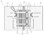
- FIG. 3 is a schematic diagram for explaining an operation example of the photoelectrochemical reaction apparatus 10.
- the light 2 is preferably sunlight, but is not limited thereto, and may be light such as a light emitting diode or an organic EL.
- the photovoltaic layer 11 absorbs the light 2 and generates and separates photoexcited electrons and holes. At this time, holes gather on the oxidation electrode layer 12 side and photoexcited electrons gather on the reduction electrode layer 13 side. Thereby, an electromotive force is generated in the photovoltaic layer 11.
- the photovoltaic layer 11 needs to have an open circuit voltage equal to or greater than the potential difference between the standard oxidation-reduction potential of the oxidation reaction and the standard oxidation-reduction potential of the reduction reaction.
- the standard redox potential of the oxidation reaction in formula (1) is 1.23 [V]
- the standard redox potential of the reduction reaction in formula (2) is ⁇ 0.11 [V].
- the open circuit voltage of the photovoltaic layer 11 is preferably equal to or greater than the potential difference including the overvoltage.
- the open circuit voltage is preferably 1.73 [V] or more.
- hydrogen ions move from the first region 14a to the second region 14b via the ion exchange membrane 15a.
- hydrogen ions move from the first region 14a to the second region 14b via the ion exchange membrane 15b in the through hole 16.
- the movement distance of the ions from the oxidation electrode layer 12 to the reduction electrode layer 13 can be greatly shortened by the movement of the hydrogen ions through the through-holes 16.
- the ion diffusibility can be enhanced while reducing the size.
- the carbon dioxide reduction reaction is a reaction that consumes hydrogen ions. For this reason, when the amount of hydrogen ions moving from the oxidation electrode layer 12 side to the reduction electrode layer 13 side is small, the efficiency of the reduction reaction is deteriorated. Therefore, it is preferable that the concentration of hydrogen ions in the first region 14a and the concentration of hydrogen ions in the second region 14b are different from each other in advance to facilitate movement of the hydrogen ions due to the concentration difference. Moreover, it is not limited to this, You may make hydroxide ion differ in the 1st area
- the photoelectrochemical reaction device of the embodiment includes an electrode layer having a porous structure.
- the surface area of the electrode layer can be increased, the diffusibility of ions and reactants can be increased, the overvoltage in the electrode layer can be reduced, and the resistance between the electrodes can be lowered.
- carbon dioxide is stable, the overvoltage tends to be high, and the conversion efficiency from light to a chemical substance tends to be low.
- unnecessary consumption of light energy such as sunlight can be suppressed, so that conversion energy from light to a carbon compound can be improved.
- the manufacturing cost can be reduced.
- the photoelectrochemical reaction cell itself functions as a partition and can isolate the product, so that it is not necessary to provide a separate product separation step.
- the photoelectrochemical reaction apparatus of the embodiment is not limited to the configuration shown in FIG.
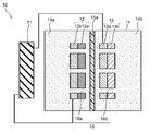
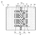
- Other structural examples of the photoelectrochemical reaction device in the embodiment will be described with reference to FIGS. 4 to 6, 8 to 10, and FIGS. 23 to 25. 4 to 6, FIG. 8 to FIG. 10, and FIG. 23 to FIG. 25 are schematic views showing other configuration examples of the photoelectrochemical reaction apparatus.
- the description of FIG. 1 is appropriately applied to portions similar to those of the photoelectrochemical reaction apparatus shown in FIG. Can be used.
- the photoelectrochemical reaction device 10 includes a photovoltaic layer 11 so as to be separated from the electrolytic solution 14.
- the oxidation electrode layer 12 is electrically connected to the first surface of the photovoltaic layer 11 and the reduction electrode layer 13 is electrically connected to the second surface using wiring or the like.
- An ion exchange membrane 15 a may be provided between the oxidation electrode layer 12 and the reduction electrode layer 13. Further, the ion exchange membrane 15b may be omitted.
- the structure has the electrolytic solution 14 between the oxidation electrode layer 12 and the reduction electrode layer 13, the resistance between the oxidation electrode layer 12 and the reduction electrode layer 13 is low, and the ion diffusibility is improved.
- one of the oxidation electrode layer 12 and the reduction electrode layer 13 may not have a porous structure. Further, the through hole 16 may not be provided.
- the gap between the oxidation electrode layer 12, the reduction electrode layer 13, and the ion exchange membrane 15a is narrow. Thereby, the resistance between the oxidation electrode layer 12 and the reduction electrode layer 13 can be lowered.
- a laminated structure without a gap may be used. In this configuration, the electrode layer does not need to have translucency.
- the electrode layer 13c includes, for example, a conductive material applicable to the reduction electrode layer 13 and a reduction catalyst. Note that the conductive material and the reduction catalyst may be the same material.
- a photoelectrochemical reaction device 10 shown in FIG. 6 is laminated on a porous conductive layer 13d and a porous conductive layer 13d as a reduction electrode layer 13 as compared with the photoelectrochemical reaction device 10 shown in FIG.
- the porous catalyst layer 13e having a porous structure For example, a mixture of conductive particles such as Nafion and Ketjen Black can be used as the porous conductive layer 13d, and a gold catalyst can be used as the porous catalyst layer 13e.
- the reduction electrode layer 13 having a nanoparticle structure can be formed by oxidizing the surface of the porous catalyst layer 13e by applying a high frequency and then electrochemically reducing the surface.
- the porous conductive layer 13d may further have a laminated structure in which each layer has different pore diameters. Depending on the laminated structure having different pore diameters, for example, the reaction difference due to the difference in the concentration of reaction products near the electrode layer or the difference in pH can be adjusted by the pore diameter to improve the efficiency.
- FIG. 7 shows an observation image of the oxidized gold catalyst by a scanning electron microscope.
- the gold catalyst 30 has a porous structure.
- this gold catalyst 30 is used for electrochemical reduction with a 0.5 M sodium carbonate aqueous solution, it is reduced to, for example, carbon monoxide with a Faraday efficiency of 90% or more.
- hydrogen is mainly produced when reduced in sulfuric acid.
- methanol is produced as a final product, it is stoichiometrically suitable to produce hydrogen and carbon monoxide at a ratio of 1: 2.
- the current density when a potential of ⁇ 0.4 V (vs RHE) is applied is about 7 mA / cm 2 .
- the reduction catalyst layer 13b having a nanoparticle structure may be formed by anodizing the surface of the gold catalyst and then performing electrochemical reduction. At this time, when electrochemical reduction is performed with a 0.5 M sodium carbonate aqueous solution, it is reduced to hydrogen as a main product.
- electrochemical reduction is performed with a 0.5 M sodium carbonate aqueous solution, it is reduced to hydrogen as a main product.
- hydrogen and CO may be generated at a ratio of 1: 2 to make a configuration suitable for methanol synthesis.
- the reduction current at this time is very large compared to a gold catalyst on a smooth plate.
- the gold catalyst may have a cubic octahedron (cubic octahedron) structure, for example.
- the gold catalyst preferably has crystal faces on the (111) face and the (100) face.
- metal catalysts such as platinum, nickel, iron, and titanium are suitable.
- the porous catalyst layer 13e having a nanoparticle structure is formed using high frequency, for example, a high frequency is applied to the conductive layer that becomes the porous catalyst layer 13e in the electrolytic solution.
- a high frequency is applied to the conductive layer that becomes the porous catalyst layer 13e in the electrolytic solution.
- a metal film that includes a metal that can be applied to the porous catalyst layer 13e and is formed by a conventional film formation method such as sputtering may be used.
- the highest potential of the high frequency is preferably not less than the oxidation potential of the porous catalyst layer 13e, and the lowest potential is preferably not more than the reduction potential of the porous catalyst layer 13e. That is, the high frequency potential periodically varies between a value equal to or higher than the oxidation potential of the porous catalyst layer 13e and a value equal to or lower than the reduction potential of the porous catalyst layer 13e.
- the oxidation potential is not particularly limited as long as the valence of the metal species is higher than the oxidation potential at which the valence can be shifted from zero to plus.
- the reduction potential may be any potential that is lower than the reduction potential at which the metal species can shift from zero valence to minus.
- the oxidation potential refers to a potential that changes from M 0 to M + , M + to M 2+, and the like, for example, considering a metal M.
- the reduction potential refers to a potential that changes, for example, from M + ⁇ M 0 or M 2+ ⁇ M + .
- the oxidation potential of the porous catalyst layer 13e is a potential that can shift the valence from zero to positive. Further, when the porous catalyst layer 13e is an oxide or the like and already has a positive valence, the potential can be shifted to a positive valence further than the value.
- the reduction potential of the porous catalyst layer 13e is a potential that can shift the valence from the positive valence to the zero valence if the porous catalyst layer 13e is a metal. Further, when the porous catalyst layer 13e is an oxide or the like and already has a positive valence, the potential can return the valence to that value.
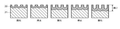
- FIG. 17 and FIG. 18 are schematic views showing a mechanism in the case of forming a nanoparticle structure using a high-frequency potential. 17 and FIG. 18 show that the oxide layer 22 of the metal layer 21 is gradually formed on the surface of the metal layer 21 over time, as the reaction proceeds from the left to the right in FIGS. 17 and 18.
- Non-Patent Document 1 when applying a high frequency having a minimum potential equal to or higher than the reduction potential of the porous catalyst layer 13e and a maximum potential equal to or higher than the oxidation potential of the porous catalyst layer 13e, it is shown in FIG. Thus, only the oxidation reaction is repeated intermittently.
- the oxidation layer 22 is formed by oxidizing the surface of the metal layer 21 by an oxidation reaction.
- the oxide layer 22 becomes thick every time the oxidation reaction occurs. When the oxide layer 22 is gradually thickened, it becomes difficult for current to pass through, so that the oxidation rate gradually decreases.
- the thickness of the oxide layer 22 is preferably not less than 1 micrometer and not more than 10 micrometers, for example.
- the formation reaction of the oxide layer 22 proceeds not only in the thickness direction of the porous catalyst layer 13e but also in the direction perpendicular to the thickness. Note that, by adjusting the high frequency, for example, the reduction reaction time may be made shorter than the oxidation reaction time.
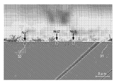
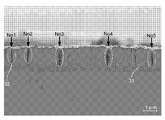
- FIG. 19 and 20 are cross-sectional observation images of a porous catalyst layer made of gold using a scanning electron microscope (SEM).
- FIG. 19 shows a high frequency (0.7-2 V (vs Hg / HgSO 4 : 0.5M, H 2 SO 4 aqueous solution) high frequency where the lowest potential is higher than the reduction potential of gold and the highest potential is higher than the oxidation potential of gold. ) Is a cross-sectional observation image of the porous catalyst layer in the case of forming by applying.
- FIG. 19 shows a high frequency (0.7-2 V (vs Hg / HgSO 4 : 0.5M, H 2 SO 4 aqueous solution) high frequency where the lowest potential is higher than the reduction potential of gold and the highest potential is higher than the oxidation potential of gold. )
- FIG. 19 shows a high frequency (0.7-2 V (vs Hg / HgSO 4 :
- the above-described high frequency having a frequency of 1000 Hz was applied to a gold film having a length of 1 cm ⁇ width 1 cm ⁇ thickness 100 ⁇ m in a sulfuric acid electrolyte solution of 0.5 M for 1 hour. It is a porous catalyst layer that is sometimes formed.
- the electrode connection part of a gold film, the back surface, etc. are sealed with the dicing film etc.
- the porous catalyst layer 31 in the case where the lowest potential is equal to or lower than the reduction potential of gold and the highest potential is higher than the oxidation potential of gold is applied. It is thicker than the porous catalyst layer 31 when formed by applying a high frequency equal to or higher than the reduction potential of gold.
- the porous catalyst layer 31 has a width of 40 ⁇ m.
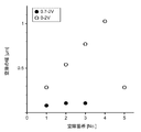
- 3-No. 3 voids 32 having a width of 50 nm or more are observed.
- five gaps 32 having a width of 50 nm or more are observed. From this, when applying a high frequency with the lowest potential being equal to or lower than the reduction potential of gold and the highest potential being equal to or higher than the oxidation potential of gold, compared to applying a high frequency with the lowest potential being equal to or higher than the reduction potential of gold, compared to applying a high frequency with the lowest potential being equal to or higher than the reduction potential of gold, It can be seen that a plurality of voids 32 extending to the surface are formed in the porous catalyst layer 31. By providing many voids 32 having a width of 50 nm or more in the porous catalyst layer 31, the surface area contributing to the reduction reaction is increased, and thus the reactivity can be increased.
- FIG. 21 is a diagram showing the width of the gap.
- the horizontal axis of FIG. The vertical axis represents the width of the voids on the surface of the porous catalyst layer.
- the widths of the five voids 32 are all 100 nm (0.1 micrometer) or more. Furthermore, No. 1 shown in FIG. 2 to No. 4 has a width of 300 nm (0.3 micrometers) or more. No. shown in FIG. 1-No. No. 5 shown in FIG. 1-No. 3 wider than the gap 32 (black circle). That is, the porous catalyst layer formed by applying a high frequency of 0-2V from FIG. 21 has a high frequency of 0.7-2V (vs Hg / HgSO 4 : 0.5M, H 2 SO 4 aqueous solution). It can be seen that there are more voids having a width of 100 nm or more than the porous catalyst layer formed by application.
- the reduction catalyst layer has, for example, three or more voids having a width of 300 nm or more in a range of 40 micrometers in width, or five or more voids having a width of 100 nm or more in a range of 40 micrometers in width. It is preferable to have.
- the surface area contributing to the reduction reaction can be sufficiently increased.
- the number and width of the gaps vary depending on, for example, the frequency of the high frequency and the application time.
- the width and number of voids are calculated from, for example, the cross-sectional observation image obtained by the SEM.
- the electrolytic solution easily enters the groove. Therefore, compared with the location where the width
- the number of voids is small and the width of the voids is narrow, so that the diffusion of reactants and products is slow and the activity is low.
- the sample of the porous catalyst layer prepared by the above method is used for the reduction reaction of carbon dioxide, it is not particularly limited after applying a high-frequency potential before the reaction, but preferably carbon dioxide is added to a 0.25 M sodium carbonate aqueous solution. Immerse in a sufficiently blown electrolyte and leave it until no air bubbles are generated from the surface. Then, using an electrolytic solution in which carbon dioxide is sufficiently blown into an aqueous sodium carbonate solution, electric potential is reduced by applying a potential of ⁇ 0.4 V (vs RHE) to the porous catalyst layer under a carbon dioxide bubbling condition. Do. In addition, an electrolytic solution such as 0.5M sulfuric acid may be used as the electrolytic solution used at this time.
- FIG. 22 is a diagram showing the current density consumed for the production of carbon monoxide in the reduction reaction test for each evaluation sample.
- the porous catalyst layer formed by applying a high frequency of 0-2V vs Hg / HgSO 4 : 0.5M, H 2 SO 4 aqueous solution
- the current density is higher than that of the porous catalyst layer formed by applying a high frequency, and it can be seen that excellent reactivity is exhibited.
- the porous catalyst layer produced by the above method is not necessarily used from an electrochemically reduced state, and may be used in an oxidized state. In this case, since the process of electrochemical reduction is included, the manufacturing process can be shortened.
- the porous catalyst layer produced by the above method can be used as, for example, the electrode layer 13c including both the conductive material and the reduction catalyst shown in FIG.
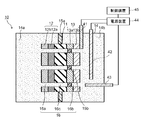
- the photoelectrochemical reaction device 10 shown in FIG. 23 is generated by the reduction reaction of CO 2 by the reduction electrode layer 13 by applying a potential to the reduction electrode layer 13 as compared with the photoelectrochemical reaction device 10 shown in FIG. The difference is that at least the selectivity of the carbon compound can be recovered (regenerated).
- the photoelectrochemical reaction device 10 shown in FIG. 23 includes a conductive layer 41 electrically connected to the reduction electrode layer 13, and an auxiliary electrode layer 42 immersed in the second region 14b.
- the conductive layer 41 has a function as a part of a working electrode when a potential is applied to the reducing electrode layer 13. That is, the reduction electrode layer 13 and the conductive layer 41 can be regarded as the working electrode.
- the conductive layer 41 for example, a layer of a material such as platinum, gold, silver, copper, an alloy such as SUS, or carbon can be used.
- the conductive layer 41 is not necessarily in contact with the reduction catalyst layer 13b, and may be in contact with the conductive layer 13a.
- the electrode layer 13c, the porous conductive layer 13d, the porous catalyst layer 13e, etc. are provided as the reduction electrode layer 13, the conductive layer 41 is any of the electrode layer 13c, the porous conductive layer 13d, and the porous catalyst layer 13e. You may touch the crab.
- the auxiliary electrode layer 42 functions as a counter electrode when a potential is applied to the reduction electrode layer 13.
- a layer of a conductive material such as platinum, gold, silver, copper, an alloy such as SUS, or carbon can be used.
- a material in which the auxiliary electrode layer 42 itself dissolves may be used. By applying the potential, all of the auxiliary electrode layer 42 may be dissolved and used up.
- the selectivity of the carbon compound is intermittently recovered (regenerated) in the photoelectrochemical reaction device 10
- the auxiliary electrode layer 42 has a material that can be regenerated or supplemented as the reaction proceeds, or the auxiliary electrode layer 42 is regenerated. Alternatively, it is preferable to have a system that can be replenished.
- the reference electrode layer 43 is an electrode layer having a function as a reference electrode when a potential is applied to the reduction electrode layer 13.
- As the reference electrode layer 43 for example, silver / silver chloride can be used.
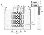
- the auxiliary electrode layer 42 and the reference electrode layer 43 may be immersed in the first region 14a. Further, each region is divided between the auxiliary electrode layer 42 and the first region 14a or the second region 14b, or between the reference electrode layer 43 and the first region 14a or the second region 14b. A membrane, a salt bridge, or the like may be provided. Furthermore, as shown in FIG. 25, an electrolytic solution that becomes the third region 14c in which the auxiliary electrode layer 42 is immersed may be provided. The electrolytic solution that becomes the third region 14c is accommodated in a container such as an electrolytic solution tank different from the electrolytic solution that becomes the first region 14a and the second region 14b, for example. The configurations shown in FIGS. 23 to 25 may be provided together with other measuring devices such as a pH meter, and can be applied to the case where a through hole is provided.
- the conductive layer 41, the auxiliary electrode layer 42, and the reference electrode layer 43 may all be immersed in the electrolytic solution 14 and electrically connected to the external power supply device 44 by wiring.
- the conductive layer 41, the auxiliary electrode layer 42, and the reference electrode layer 43 are connected to the photoelectrochemical reaction device 10 only when a potential is applied to the reduction electrode layer 13 in order to restore (regenerate) the selectivity of the carbon compound. May be installed.
- the photoelectrochemical reaction device 10 a reduction electrode recovery (regeneration) device (reduction electrode cleaning device) including the conductive layer 41, the auxiliary electrode layer 42, the reference electrode layer 43, the power supply device 44, and the control device 45, It can also be regarded as an electrochemical reaction system comprising
- the power supply device 44 is provided outside the electrolytic solution 14, for example.
- the power supply device 44 is electrically connected to the conductive layer 41, the auxiliary electrode layer 42, and the reference electrode layer 43 through, for example, wiring.
- the power supply device 44 has a function of applying a potential to the reduction electrode layer 13.
- the power supply device 44 is provided outside the electrolyte solution 14, for example.
- the power supply device 44 includes, for example, a power supply circuit and a control circuit that controls the power supply circuit.
- the control circuit includes, for example, a CPU (Central Processing Unit), a memory, a logic circuit, and the like, and generates and outputs a control signal input to the power supply circuit.
- the power supply device 44 may have an electrochemical measurement function such as impedance measurement, constant voltage current measurement, constant current voltage measurement and the like by including, for example, an electrochemical measurement device.
- an electrochemical measurement device such as a temperature sensor or a pH sensor, it may have a measurement function other than electrochemical measurement such as temperature measurement or pH measurement.
- the control device 45 is provided outside the electrolytic solution 14, for example.
- the control device 45 has a function of controlling a condition for applying a potential by the power supply device 44.
- the control device 45 includes, for example, a CPU (Central Processing Unit), a memory, a logic circuit, and the like, and generates and outputs a control signal input to the power supply device 44.
- the current flowing through the reduction electrode layer 13 during the reduction reaction is monitored by a sensor or the like, and the potential of the control signal is controlled according to the current value, so that the necessity of potential application by the power supply device 44 or the value of the potential to be applied is determined. May be controlled.
- the control device 45 may have a function of controlling measurements that can be performed by the power supply device 44. It is not limited to this, For example, you may have other control functions, such as a gas component composition analysis and a solution component composition analysis.
- a potential higher than the oxidation potential of the reduction catalyst layer 13b and a potential lower than the reduction potential of the reduction catalyst layer 13b are separately applied between the reduction electrode layer 13 and the auxiliary electrode layer 42, or the reduction electrode
- An AC potential having a highest potential that is more noble than the oxidation potential of the reduction catalyst layer 13b and a lowest potential that is lower than the reduction potential of the reduction catalyst layer 13b is applied between the layer 13 and the auxiliary electrode layer.
- the oxidation potential of the reduction catalyst layer 13b is a potential that can shift the valence from zero to positive if the reduction catalyst layer 13b is a metal. Further, when the reduction catalyst layer 13b is an oxide or the like and already has a positive valence, the potential can be shifted to a positive valence further than the value.
- the reduction potential of the reduction catalyst layer 13b is a potential that can shift the valence from the positive valence to the zero valence if the reduction catalyst layer 13b is a metal. Further, when the reduction catalyst layer 13b is an oxide or the like and already has a positive valence, the potential can return the valence to that value.
- the reduction catalyst layer 13b When the potential is applied, for example, when the CO selectivity and the current value at the time of generation are decreased, the reduction catalyst layer 13b is washed, and the CO selectivity and the current value at the time of generation are reduced. It can be recovered (regenerated). At this time, the electrolyte solution may be changed to be suitable for cleaning the catalyst layer.
- the oxidation potential and the reduction potential are preferably applied one or more times each. Further, it is preferable to repeatedly apply the potential until the change in current value during the reaction becomes substantially constant. At this time, it is preferable that the value of the current flowing between the electrodes can be measured.
- the photoelectrochemical reaction apparatus 10 when using the photoelectrochemical reaction apparatus 10, it is preferable to apply and sweep the potential once or more before use. Moreover, it is preferable to use an apparatus that can analyze or monitor the composition of the product resulting from the reduction reaction or the current value during the reaction. Thus, the potential can be automatically applied according to the composition of the product and the current value during the reaction.
- the potential is at least once or more. It is preferable to perform the application operation.
- the potential application operation is preferably performed, for example, in conjunction with the photoelectrochemical reaction device 10 in a system in which an algorithm representing the potential application operation is incorporated.
- Table 1 is a diagram showing the relationship between the CO 2 reduction reaction and the CO production selectivity in the evaluation sample.
- an evaluation sample using a gold nanoparticle electrode as a reduction electrode and a CO 2 saturated sodium hydrogen carbonate aqueous solution as an electrolyte solution was used. Apply an electric potential of .4 V (vs RHE), and calculate the average value of the production selectivity of carbon monoxide, which is a reduction product produced during one hour after the reaction. Thereafter, the used reduction electrode is washed with pure water, naturally dried, and the average value of the CO production selectivity is calculated repeatedly.
- the fourth CO 2 reduction reaction reduces the CO production selectivity to less than 80%. Therefore, for the evaluation sample using the above gold nanoparticle electrode as the working electrode, the platinum electrode as the counter electrode, the silver / silver chloride electrode as the reference electrode, and the CO 2 saturated sodium hydrogen carbonate aqueous solution as the electrolyte,
- the operation of applying the potential to the working electrode while sweeping the potential at 150 mV / sec in the range of 1.3 to +1.4 V (vs Ag / AgCl) is repeated 100 times. For example, in a single potential application operation, the potential is swept from 0 V to ⁇ 1.3 V, applied, and then the potential is swept from ⁇ 1.3 V to 1.4 V, and then from 1.4 V to 0 V The potential is swept up to
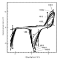
- FIG. 26 is a diagram illustrating the relationship between the applied potential and the current density in the potential application operation.
- the horizontal axis represents the applied potential
- the vertical axis represents the generated current density.
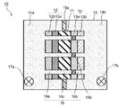
- the 8 includes a stirrer 17a and a stirrer 17b in addition to the components of the photoelectrochemical reaction device 10 shown in FIG.
- the stirrer 17a is provided in the first region 14a, and the stirrer 17b is provided in the second region 14b.
- the pH of the second region 14b is preferably lower than the pH of the first region 14a.
- the surface pH and the internal pH may be different.
- a pH distribution in which the pH on the surface of the reduction electrode layer 13 is higher than the pH on the surface of the oxidation electrode layer 12 may be formed.
- the first region 14a and the second region 14b are stirred by the stirrer 17a and the stirrer 17b, so that the uniformity of each pH can be improved. it can. Further, by promoting the movement of ions, the resistance between the first region 14a and the second region 14b can be lowered, so that the conversion efficiency can be increased.
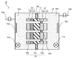
- the photoelectrochemical reaction device 10 shown in FIG. 9 includes, in addition to the components of the photoelectrochemical reaction device 10 shown in FIG. 1, a stirrer 17a and a stirrer 17b, a pH sensor 18a and a pH sensor 18b, and a supply channel 19a. And a supply channel 19b.
- Each of the pH sensor 18a and the pH sensor 18b has a measurement electrode layer.
- the measurement electrode layer of the pH sensor 18a is in contact with the first region 14a
- the measurement electrode layer of the pH sensor 18b is in contact with the second region 14b.
- the pH of the electrolyte solution 14 can be measured by the pH sensors 18a and 18b.
- a reduction catalyst may be used for the measurement electrode layer of the pH sensor 18b, and the carbon compound may be generated by causing a reduction reaction in the measurement electrode layer.
- the carbon compound may be generated using light energy by electrically connecting the oxidation electrode layer 12 or the reduction electrode layer 13 to the pH sensor measurement electrode layer. Moreover, it is not limited to light energy, It may be an external power supply or other natural energy.
- a carbon compound different from the carbon compound generated in the reduction electrode layer 13 may be generated. For example, carbon monoxide may be generated by the reduction electrode layer 13 and formic acid may be generated by the measurement electrode layer of the pH sensor 18b.
- the measurement electrode layer of the pH sensor 18b may be connected to an external power source and used as the second reduction electrode layer.
- formic acid generated by the reduction reaction of the reduction electrode layer 13 which is the first reduction electrode layer And the like may be further reduced by the second reduction electrode layer to generate methanol or the like.
- the position of the measurement electrode layer of the pH sensor 18b is arbitrary, and may be provided in the vicinity of the oxidation electrode layer 12, for example.
- the measurement electrode layer of the pH sensor 18a may be used for the oxidation reaction.
- the supply channel 19a has a function of supplying a reactant when the pH of the electrolyte solution 14 measured by the pH sensor 18a is outside the reference range
- the supply channel 19b is provided for the electrolyte solution 14 measured by the pH sensor 18b. It has a function of supplying the reactant when the pH is outside the reference range.
- a valve may be provided in the supply channels 19a and 19b, and the valve may be controlled by a control circuit having an arithmetic circuit such as a CPU so that the valve opens when the measured value of the pH sensor is outside the reference range.
- an electrolytic solution containing a reactive substance may be supplied via the supply channel 19a and the supply channel 19b.
- the photoelectrochemical reaction device 10 shown in FIG. 10 includes a pH sensor 18a and a pH sensor 18b, a supply channel 19a and a supply channel 19b in addition to the components of the photoelectrochemical reaction device 10 shown in FIG.
- the supply channel 19a is in contact with the first region 14a of the electrolyte solution 14 at two or more locations
- the supply channel 19b is in contact with the second region 14b of the electrolyte solution 14 at two or more locations.
- the pH sensor 18a may be provided so as to be in contact with the supply channel 19a
- the pH sensor 18b may be provided so as to be in contact with the supply channel 19b.
- the electrolyte solution 14 can be circulated through the supply channel 19a and the supply channel 19b. Moreover, since it circulates by natural convection when it gives temperature distribution to the electrolyte solution 14 with sunlight etc., it is preferable. Therefore, in the electrolytic solution 14, not only the pH but also the temperature and concentration can be easily made uniform. Moreover, since it is not necessary to provide a stirrer at this time, the energy accompanying stirring is reduced, and the system can be simplified.
- the electrolytic solution 14 may be circulated using a circulation pump.
- the entire electrolytic solution 14 can be prepared at a time.
- the reactant may be supplied in the electrolyte solution or the like via the supply channel 19a and the supply channel 19b according to the measured values of the pH sensors 18a and 18b.
- ions may be circulated more efficiently by causing a temperature difference in the electrolytic solution by using heat raised by irradiating the photovoltaic layer 11 with light, for example.
- ion movement can be promoted by convection other than ion diffusion.
- a temperature regulator that adjusts the temperature of the electrolytic solution is provided in a container that accommodates the electrolytic solution 14 or in the electrolytic solution supply channel, and the oxidation-reduction reaction can be controlled by temperature control.
- FIG. 27 is a diagram showing a configuration of the photoelectrochemical reaction device according to the present example.
- the through-hole 16 and the ion exchange membrane 15b are not provided as compared with the photoelectrochemical reaction device 10 shown in FIG. 1, and the photovoltaic layer 11 is formed in the first region 14a.
- the electrode layer 13c which is immersed and has the reduction catalyst function shown in FIG. 5 as the reduction electrode layer 13 is provided, and the ion exchange membrane 15a is provided between the first region 14a and the second region 14b.
- the difference is that the second surface of the layer 11 and the reduction electrode layer 13 are electrically connected by wiring or the like.
- the photoelectrochemical reaction device 10 includes an ammeter 46 between the second surface of the photovoltaic layer 11 and the reducing electrode layer 13.
- the photoelectrochemical reaction device 10 includes a control device 47 electrically connected to the ammeter 46.
- a control device 47 may be provided outside the photoelectrochemical reaction device 10.
- the ammeter 46 has a function of measuring the current flowing through the reduction electrode layer 13.
- the control device 47 has a function of controlling measurement conditions by the ammeter 46, for example.
- the control device 47 includes, for example, a CPU x, a memory, a logic circuit, and the like, and generates and outputs a control signal input to the ammeter 46.
- the current value can be measured by the ammeter 46, and the obtained current value data can be sent to the control device 47 in real time.
- the control device 47 may have a function of interrupting the operation of the photoelectrochemical reaction device 10 and shifting to a process when the data of the current value sent is below the reference value. Good. That is, the control device 47 may have a function as the control device 45. Further, the plurality of photoelectrochemical reaction devices 10 may be controlled by the control device 47.
- a three-junction type (pin junction type) photovoltaic layer having a length of 1 cm ⁇ width of 1 cm ⁇ thickness of 500 nm was used.
- an oxidation electrode layer having a conductive layer 12a made of an ITO layer having a thickness of 70 nm and an oxidation catalyst layer 12b made of a cobalt oxide layer having a thickness of 15 nm was used.
- a reduction electrode layer having a length of 1 cm, a width of 1 cm, and a thickness of 1 mm comprising an electrode layer 13c containing gold as a conductive material and containing a porous gold catalyst as a reduction catalyst was used.
- a Selemion (registered trademark) membrane was used as the ion exchange membrane 15a.
- a 0.25M sodium carbonate aqueous solution into which carbon dioxide was sufficiently blown was used as the electrolytic solution in the second region 14b in which the reduction electrode layer 13 was immersed.
- ⁇ [R (CO) ⁇ ⁇ G 0 ] / [P ⁇ S] ⁇ 100 (3)
- ⁇ represents the conversion efficiency (%) from light to carbon monoxide
- R (CO) represents the carbon monoxide production rate (mol / sec)
- ⁇ G 0 represents the combustion of carbon monoxide.
- P represents the energy intensity (1000 W / m 2 ) of the irradiation light
- S represents the light receiving area (cm 2 ) of the irradiation light. .
- Table 2 is a table showing the conversion efficiency from light to carbon monoxide when the CO 2 reduction reaction is performed.
- the conversion efficiency from light to carbon monoxide in the case where a 0.5 M potassium borate aqueous solution was used as the electrolytic solution in the first region 14a was about 1.5%.
- the conversion efficiency from light to carbon monoxide was about 0.5% when a 0.25M sodium carbonate aqueous solution into which carbon dioxide was sufficiently blown was used as the electrolyte in the first region 14a.
- the conversion efficiency from light to carbon monoxide was about 1.1% when a 0.25M aqueous sodium carbonate solution into which carbon dioxide was not blown was used as the electrolyte in the first region 14a.
- the conversion efficiency from light to carbon monoxide when using a 0.25M sodium carbonate aqueous solution in which carbon dioxide is not blown as the electrolyte in the first region 14a is as follows.
- the conversion efficiency from light to carbon monoxide was higher when a 0.25M sodium carbonate aqueous solution into which carbon dioxide was sufficiently blown was used as the electrolyte solution 14a.
- the overvoltage during the oxidation reaction by the oxidation electrode layer 12 is suppressed by the pH of the electrolyte solution in the first region 14a not being lowered.
- the conversion efficiency can be improved by blowing CO 2 without preparing an electrolytic solution, for example, so that the cycle of the oxidation-reduction reaction proceeds permanently. Can be made.
Landscapes
- Chemical & Material Sciences (AREA)
- Organic Chemistry (AREA)
- Engineering & Computer Science (AREA)
- Chemical Kinetics & Catalysis (AREA)
- Electrochemistry (AREA)
- Materials Engineering (AREA)
- Metallurgy (AREA)
- Inorganic Chemistry (AREA)
- Electrolytic Production Of Non-Metals, Compounds, Apparatuses Therefor (AREA)
- Power Engineering (AREA)
- Microelectronics & Electronic Packaging (AREA)
Abstract
光から炭素化合物への変換効率を高める。電解液と、電解液に浸漬された酸化電極層と、電解液に浸漬された還元電極層と、酸化電極層に電気的に接続された第1の面と、第1の面に対向し還元電極層に電気的に接続された第2の面とを有し、第1の面または第2の面に照射された光のエネルギーにより電荷分離を行う光起電力層と、を具備する。酸化電極層および還元電極層の少なくとも一方は、細孔を含む多孔質構造を有する。
Description
実施形態の発明は、光電気化学反応装置に関する。
近年、エネルギー問題や環境問題の観点から、植物の光合成を模倣して太陽光を電気化学的に化学物質に変換する人工光合成技術の開発が進められている。太陽光を化学物質に変換してボンベやタンクに貯蔵する場合、太陽光を電気に変換して蓄電池に貯蔵する場合に比べて、エネルギーの貯蔵コストを低減することができ、また貯蔵ロスも少ないという利点がある。
太陽光を電気化学的に化学物質へ変換する光電気化学反応装置としては、例えば二酸化炭素(CO2)を還元する還元触媒を有する電極と、水(H2O)を酸化する酸化触媒を有する電極とを備え、これら電極をCO2が溶解した水中に浸漬させる二電極方式の装置が知られている。このとき、各電極は電線等を介して電気的に接続される。酸化触媒を有する電極においては、光エネルギーによりH2Oを酸化して酸素(1/2O2)を得ると共に、電位を得る。還元触媒を有する電極においては、酸化反応を生起する電極から電位を得ることによって、CO2を還元して蟻酸(HCOOH)等を生成する。このように、二電極方式の装置においては、CO2の還元電位を2段励起により得ているため、太陽光から化学エネルギーへの変換効率が0.04%程度と非常に低い。また、光電気化学反応装置として、例えばGaNを用いて光電変換を行いその表面で水を酸化し、電気的に接続された銅板によってCO2を還元する装置が知られている。しかしながら、変換効率が0.2%と低い。
また、一対の電極で光起電力層を挟持した積層体(シリコン太陽電池等)を用いた光電気化学反応装置も検討されている。光照射側の電極では、光エネルギーにより水(2H2O)を酸化して酸素(O2)と水素イオン(4H+)を得る。反対側の電極では、光照射側電極で生成した水素イオン(4H+)と光起電力層に生じた電位(e-)とを用いて、化学物質として水素(2H2)等を得る。また、シリコン太陽電池を積層させた電気化学反応装置も知られている。この場合の太陽光から化学エネルギーへの変換効率は高いが、水素は貯蔵や輸送が不便である。エネルギー問題や環境問題を考えると、水素ではなく、貯蔵や輸送が容易な炭素化合物に変換することが好ましい。
Y.Chen,et al.,Journal of the American Chemical Society vol.134.pp.19969(2012)
W.Zhu,et al.,Journal of the American Chemical Society vol.135.pp.16833(2013)
実施形態の発明が解決しようとする課題は、光から炭素化合物への変換効率を高めることである。
実施形態の光電気化学反応装置は、電解液と、電解液に浸漬された酸化電極層と、電解液に浸漬された還元電極層と、酸化電極層に電気的に接続された第1の面と、第1の面に対向し還元電極層に電気的に接続された第2の面とを有し、第1の面または第2の面に照射された光のエネルギーにより電荷分離を行う光起電力層と、を具備する光電気化学反応装置である。酸化電極層および還元電極層の少なくとも一つは、細孔を含む多孔質構造を有する。
図1は、光電気化学反応装置の構成例を示す模式図である。図1に示す光電気化学反応装置10は、光起電力層11と、酸化電極層12と、還元電極層13と、電解液14と、イオン交換膜15aと、イオン交換膜15bと、を具備する。さらに、光電気化学反応装置10は、貫通孔16を有する。貫通孔16は、酸化電極層12を貫通する貫通孔16aと、還元電極層13を貫通する貫通孔16bと、光起電力層11を貫通する貫通孔16cと、を有する。図1に示すように、貫通孔16aないし貫通孔16cは、互いに連通するように設けられている。なお、貫通孔16aないし貫通孔16cの径は、それぞれ異なっていてもよい。また、必ずしも貫通孔16aないし貫通孔16cを設けなくてもよい。さらに貫通孔16aないし貫通孔16cは、互いに連通しなくても良い。
光起電力層11は、照射された太陽光等の光のエネルギーにより電荷分離を行う機能を有する。電荷分離により発生した正孔は酸化電極層12側に移動し、電子は還元電極層13側に移動する。これにより、光起電力層11は、起電力を発生することができる。光起電力層11は、対向する第1の面および第2の面を有する。光起電力層11としては、例えばpn接合型またはpin接合型の光電変換層を用いることができる。なお、複数の光電変換層を積層することにより光起電力層11を形成してもよい。
光起電力層11の貫通孔16cは、例えばエッチング等により光起電力層11の一部を除去することにより形成される。なお、複数の開口工程により貫通孔16cを形成してもよい。
図2は、光起電力層11の構造例を示す模式図である。図2に示す光起電力層11は、反射層111と、光電変換層112と、光電変換層113と、光電変換層114と、を具備する。なお、必ずしも反射層111を設けなくてもよい。
反射層111は、光反射性を有する材料で構成される。反射層111としては、例えば金属層または半導体層の積層からなる分布型ブラッグ反射層が挙げられる。反射層111を設けることにより、光電変換層112ないし光電変換層114で吸収できなかった光を反射させて光電変換層112ないし光電変換層114のいずれかに入射することができるため、光から化学物質への変換効率を高めることができる。
反射層111としては、例えばAg、Au、Al、Cu等の金属、それら金属を少なくとも1つ含む合金等の層が挙げられる。なお、反射層111を第1の反射層と第2の反射層との積層としてもよい。このとき、第1の反射層は、光反射性および導電性を有し、第2の反射層は、透光性を有する。第1の反射層としては、上記金属材料または合金を用いることができる。第2の反射層は、光学的距離を調整して光反射性を高めるために設けられる。第2の反射層としては、光透過性を有し、n型半導体層とオーミック接触が可能な材料で形成することが好ましい。第2の反射層としては、例えばインジウム錫酸化物(Indium Tin Oxide:ITO)、酸化亜鉛(ZnO)、フッ素を含む酸化錫(Fluorine-doped Tin Oxide:FTO)、アルミニウムを含む酸化亜鉛(Aluminum-doped Zinc Oxide:AZO)、アンチモンを含む酸化錫(Antimony-doped Tin Oxide:ATO)等の透光性金属酸化物の層が挙げられる。
光電変換層112は、反射層111上に設けられる。光電変換層112は、下部側から順に積層されたn型のアモルファスシリコン(a-Si)からなるn型半導体層112a、真性(intrinsic)のアモルファスシリコンゲルマニウム(a-SiGe)からなるi型半導体層112b、およびp型の微結晶シリコン(uc-Si)からなるp型半導体層112cを具備する。i型半導体層112bは、400nm程度の短波長領域の光を吸収する層である。よって、光電変換層112では、短波長領域の光エネルギーによって、電荷分離が生じる。
光電変換層113は、光電変換層112上に設けられる。光電変換層113は、下部側から順に積層されたn型のa-Siからなるn型半導体層113a、真性のa-SiGeからなるi型半導体層113b、およびp型のuc-Siからなるp型半導体層113cを具備する。i型半導体層113bは、600nm程度の中間波長領域の光を吸収する層である。よって、光電変換層113では、中間波長領域の光エネルギーによって、電荷分離が生じる。
光電変換層114は、光電変換層113上に設けられる。光電変換層114は、下部側から順に積層されたn型のa-Siからなるn型半導体層114a、真性(intrinsic)のa-Siからなるi型半導体層114b、およびp型のuc-Siからなるp型半導体層114cを具備する。i型半導体層114bは、700nm程度の長波長領域の光を吸収する層である。よって、光電変換層114では、長波長領域の光エネルギーによって、電荷分離が生じる。
p型半導体層またはn型半導体層は、例えば半導体材料にドナーまたはアクセプタとなる元素を添加することにより形成することができる。なお、図2に示す光起電力層11では、半導体層としてシリコン、ゲルマニウム等を含む半導体層を用いているが、これに限定されず、例えば化合物半導体層等を用いることができる。化合物半導体層としては、例えばGaAs、GaInP、AlGaInP、CdTe、CuInGaSe等を含む半導体層を用いることができる。また、光電変換が可能であればTiO2やWO3のような半導体層を用いてもよい。さらに、各半導体層は、単結晶、多結晶、またはアモルファスであってもよい。また、光電変換層に酸化亜鉛層を設けてもよい。
図2に示す光起電力層11では、p型半導体層114cの上面が第1の面となり、n型半導体層112aに接する反射層111の下面が第2の面となる。以上のように、図2に示す光起電力層11は、光電変換層112ないし光電変換層114を積層することで、太陽光の幅広い波長の光を吸収することができ、太陽光エネルギーをより効率良く利用することができる。このとき、各光電変換層が直列に接続されているため高い電圧を得ることができる。これに限定されず、例えば並列接続で複数の光電変換層を電気的に接続してもよい。また、2接合型、単層型の光起電力層を用いてもよい。また、図2では3つの光電変換層の積層を有する光起電力層の例について説明したが、これに限定されず、2つまたは4つ以上の光電変換層の積層を有していてもよい。また、複数の光電変換層の積層に代えて、1つの光電変換層を用いてもよい。以上が図2に示す光起電力層11の構造例の説明である。
図1に示す酸化電極層12は、光起電力層11の第1の面に電気的に接続される。酸化電極層12は、水の酸化反応により水素イオンを生成する機能を有する。酸化電極層12は、導電材料および酸化触媒を含む。例えば、酸化電極層12は、導電材料を含む導電層12aと、導電層12aに積層され酸化触媒を含む酸化触媒層12bとを有する。酸化触媒層12bは、例えば薄膜状、格子状、粒子状、ワイヤー状であってもよい。なお、酸化触媒および導電材料を含む単層によって酸化電極層12を構成してもよい。
酸化電極層12は、例えば光起電力層11におけるp型半導体層114cとオーミック接触が可能な導電材料で構成される。導電材料としては、例えばAg、Au、Al、およびCuの少なくとも1つを含む材料が挙げられる。これに限定されず、例えばITO、ZnO、FTO、AZO、またはATO等の透光性金属酸化物を導電材料として用いてもよい。酸化電極層12は、例えば金属と透光性金属酸化物との積層、金属とその他の導電材料とを含む層、または透光性金属酸化物とその他の導電材料とを含む層であってもよい。
光が酸化電極層12を介して光起電力層11に照射する場合、酸化電極層12は、透光性を有する必要がある。このとき、酸化電極層12の光の透過率は、例えば酸化電極層12に照射される光の照射量の少なくとも10%以上、より好ましくは30%以上であることが好ましい。
酸化触媒としては、水を酸化するための活性化エネルギーを減少させる材料、言い換えると、水の酸化反応により酸素と水素イオンを生成する際の過電圧を低下させる材料が挙げられる。例えば、イリジウム、白金、コバルト、マンガン触媒等が挙げられる。また、酸化触媒としては、二元系金属酸化物、三元系金属酸化物、または四元系金属酸化物などを用いることができる。二元系金属酸化物としては、例えば酸化マンガン(Mn-O)、酸化イリジウム(Ir-O)、酸化ニッケル(Ni-O)、酸化コバルト(Co-O)、酸化鉄(Fe-O)、酸化スズ(Sn-O)、酸化インジウム(In-O)、または酸化ルテニウム(Ru-O)等が挙げられる。三元系金属酸化物としては、例えばNi-Co-O、La-Co-O、Ni-La-O、Sr-Fe-O等が挙げられる。四元系金属酸化物としては、例えばPb-Ru-Ir-O、La-Sr-Co-O等が挙げられる。なお、これに限定されず、酸化触媒としてRu錯体またはFe錯体等の金属錯体を用いることもできる。また、複数の材料を混合してもよい。
酸化電極層12の貫通孔16aは、例えば予め酸化電極層12に形成されていてもよい。例えば、エッチング等により酸化電極層12の一部を除去することで貫通孔16aを形成することができる。なお、複数の開口工程により貫通孔16aを形成してもよい。
還元電極層13は、光起電力層11の第2の面に電気的に接続される。還元電極層13は、二酸化炭素の還元反応による炭素化合物を生成する機能を有する。還元反応により生成される炭素化合物は、還元触媒の種類等によって異なる。例えば、一酸化炭素(CO)、蟻酸(HCOOH)、メタン(CH4)、メタノール(CH3OH)、エタン(C2H6)、エチレン(C2H4)、エタノール(C2H5OH)、ホルムアルデヒド(HCHO)、アセトアルデヒド(CH3CHO)、酢酸(CH3COOH)、エチレングリコール(HOCH2CH2OH)、1-プロパノール(CH3CH2CH2OH)、イソプロパノール(CH3CHOHCH3)等の炭素化合物が挙げられる。
還元電極層13は、導電材料および還元触媒を含む。例えば、還元電極層13は、導電材料を含む導電層13aと、導電層13aに積層され還元触媒を含む還元触媒層13bと、を有する。還元触媒層13bは、例えば薄膜状、格子状、粒子状、ワイヤー状であってもよい。これに限定されず、導電材料および還元触媒の両方を含む単層で還元電極層13を構成してもよい。なお、光起電力層11に反射層111を設けない場合、還元電極層13は、光起電力層11におけるn型半導体層112aとオーミック接触が可能な材料の層であってもよい。
導電材料としては、例えばAg、Au、Al、Pd、Sn、Bi、もしくはCu等の金属、または当該金属を複数含む、例えばSUSのような合金材料を用いることができる。例えば、上記材料の基板により導電層13aを構成することにより、光起電力層11、酸化電極層12、還元電極層13からなる光電気化学反応セルの機械的強度を高めることができる。これに限定されず、例えばITO、ZnO、FTO、AZO、またはATO等の透光性金属酸化物を導電材料として用いてもよい。還元電極層13は、例えば金属と透光性金属酸化物との積層、金属とその他の導電材料とを含む層、または透光性金属酸化物とその他の導電材料とを含む層であってもよい。また、導電材料としてシリコンやゲルマニウム等の半導体基板、導電性樹脂、導電性のイオン交換膜等を用いてもよい。また、アイオノマー等の樹脂材料を用いてもよい。
還元触媒としては、二酸化炭素を還元するための活性化エネルギーを減少させる材料、言い換えると、二酸化炭素の還元反応により炭素化合物を生成する際の過電圧を低下させる材料が挙げられる。例えば、金属材料または炭素材料を用いることができる。金属材料としては、例えばAu、Ag、Cu、Pt、Ni、Zn、またはPd等を用いることができる。炭素材料としては、例えば炭素、グラフェン、カーボンナノチューブ(Carbon Nanotube:CNT)、フラーレン、またはケッチェンブラック等を用いることができる。なお、これに限定されず、還元触媒として例えばRu錯体またはRe錯体等の金属錯体を用いてもよい。また、複数の材料を混合してもよい。
さらに、還元電極層13は、電解液14を通過させるための細孔を含む多孔質構造を有する。多孔質構造は、例えば細孔を有しない材料を加工して細孔を形成する方法、多孔質材料を用いる方法等により形成される。
多孔質構造の還元電極層13に適用可能な材料としては、上記材料に加え、例えばケッチェンブラックやバルカンXC-72等のカーボンブラック、活性炭、金属微粉末等が挙げられる。例えば、上記多孔質構造の還元電極層13に適用可能な材料を導電層13aに用いてもよい。
多孔質構造は、5nm以上100nm以下の細孔分布を有することが好ましい。上記細孔分布を有することにより触媒活性を高めることができる。さらに、多孔質構造は、複数の細孔分布ピークを有することが好ましい。これにより、表面積の増大、イオンや反応物質の拡散性の向上、高い導電性の全てを同時に実現することができる。例えば、5マイクロメートル以上10マイクロメートル以下の細孔分布を有する導電層13aに100nm以下の上記還元触媒に適用可能な金属または合金の微粒子(微粒子状の還元触媒)を含む還元触媒層13bを積層してもよい。このとき、微粒子も多孔質構造を有していてもよいが、導電性や反応サイトと物質拡散の関係から必ずしも多孔質構造を有していなくてもよい。また、上記微粒子を他の材料に坦持させてもよい。このようにすることで触媒層の導電性とガスの拡散性、触媒粒子とガス状の反応分子やイオンとの接触確率が向上し、反応効率が良くなる。
上記微粒子の径は、小さい方が好ましく、例えば粒子径分布において、粒径10nm以下の微粒子が全体の50%を超える、好ましくは70%以上であることが好ましい。また、平均粒子径Rおよび標準偏差σが、R+2σ<10nmの関係を満たすことが好ましい。
ここで、微粒子として金粒子が坦持されたケッチェンブラック粒子を有する還元触媒層の還元反応試験の一例について説明する。還元反応試験用の評価サンプルの製造方法例としては、金粒子が坦持されたケッチェンブラック粒子(以下単にケッチェンブラック粒子ともいう)をナフィオン(登録商標)とを特に限定されないが好ましくは1:3(質量比)程度で混合することでペーストを作製する。次に、上記ペーストをカーボンペーパーに塗布する。さらに、カーボンペーパーにおけるペーストの塗布面の反対面とSUS基板が向かい合うようにカーボンペーパーとSUS基板とを導電性カーボンペーストを挟んで貼り合わせ、エポキシ樹脂によりSUS基板の露出面や電極接続部分等を封止することで評価サンプルを作製する。
図11ないし図14は、評価サンプルにおける300個分の金粒子の粒径分布を示す図である。図11は(金粒子質量/(金粒子質量+ケッチェンブラック質量))×100で求められる金粒子質量%が1質量%である評価サンプルの粒径分布であり、図12は上記金粒子質量%が5質量%である評価サンプルの粒径分布であり、図13は上記金粒子質量%が19質量%である評価サンプルの粒径分布であり、図14は上記金粒子質量%が24質量%である評価サンプルの粒径分布である。各評価サンプルにおける金粒子の平均粒子径Rおよび標準偏差σを、図11ないし図14のそれぞれに示す。なお、金粒子は、例えば電子顕微鏡またはX線結晶構造解析等により特定される。また、金粒子の粒子径は、例えばJISH7803ないしJISH7805に準じる測定方法を用いて測定される。
図15および図16は、還元反応試験において、縦1cm×横1cm×厚さ1mmの上記評価サンプルに対し、0.25Mの炭酸ナトリウム水溶液に二酸化炭素を十分吹き込んだ電解液中で-0.4V(vs RHE(Reversible Hydrogen Electrode:RHE))の電位を印加したときの一酸化炭素の生成選択率(CO生成選択率)を示す図である。このとき、ケッチェンブラック粒子を含む層の厚さは250マイクロメートルである。なお、一酸化炭素の生成選択率とは、還元反応により生成される全ての物質のうちの一酸化炭素の生成割合である。
図15は、金粒子の平均粒子径と一酸化炭素の生成選択率との関係を示す図である。図15に示すように、上記金粒子質量%が5質量%、19質量%、および24質量%である評価サンプルでは、一酸化炭素の生成選択率が50%を超える。これに対し、上記金粒子質量%が1質量%である評価サンプルでは、一酸化炭素の生成選択率が50%未満であることがわかる。また、上記金粒子質量%が低くても一酸化炭素の生成選択率が50%を超える場合があることがわかる。さらに、金粒子の平均粒子径と一酸化炭素の生成選択率との間には顕著な相関がないことがわかる。
一方、図16は、粒径5nm以下の金粒子の割合と一酸化炭素の生成選択率との関係を示す図である。なお、図16における曲線は、各評価サンプルの値に基づく近似曲線である。図16に示すように、粒径5nm以下の金粒子の割合が全微粒子数の25%を超える評価サンプルにおいて、一酸化炭素の生成選択率が50%を超えていることがわかる。
図11ないし図16から、一酸化炭素等の炭素化合物の生成選択率を高めるためには、金粒子の含有量を増やすだけでなく、粒子径の小さい金粒子の割合を多くすることが好ましいと考えられる。例えば、粒子径が大きい粒子は表面積が大きいが、還元反応に寄与する活性面が小さいため、炭素化合物の生成選択率が上昇しにくい。これに対し、粒子径が小さくなると粒子の表面に原子のエッジ面が露出し易くなるため活性面の割合が増える。よって、還元反応に寄与する面積が増え、炭素化合物の生成選択率を高めることができる。
活性面の割合は、粒子径が小さくなるほど指数関数的に大きくなる。例えば、5nm以下の粒子径であれば十分な活性面を有しているといえる。図11ないし図16から鑑みると、一酸化炭素の生成選択率を50%よりも高くするためには、例えば粒径5nm以下の金粒子が金粒子全体の25%以上含まれていることが好ましい。
非特許文献2では、金粒子の平均粒子径が4nm~10nmである。しかしながら、上記と同様の還元反応試験により-0.4V(vs RHE)の電位を印加したときの一酸化炭素の生成選択率は、30%程度であると考えられる(非特許文献2、図1c)。このことから、非特許文献2では、粒径5nm以下の金粒子の割合が金粒子全体の25%未満であると考えられる。このように、一酸化炭素等の炭素化合物の生成選択率を高めるためには、還元触媒層の表面積を大きくするだけでなく、活性面の面積を大きくすることが重要である。
還元電極層13は、界面活性剤を含むことが好ましい。界面活性剤を用いることにより、反応後に生成したガス等が還元電極層13から脱着しやすくなる。また、界面活性剤を用いることにより、多孔質構造に微粒子が分散して吸着することにより、反応を促進させることができる。
界面活性剤としては、例えばポリビニルピロリドン、ポリビニルアルコール等の親水基を有するビニル化合物、およびその誘導体やポリマー等を用いることができる。また、これらと同等の機能を有する材料であれば他の材料を用いてもよい。
還元電極層13は、イオン交換樹脂を含むことが好ましい。例えばナフィオン(登録商標)等のイオン交換樹脂を用いることにより、反応に寄与するイオンの吸着等を制御することができる。また、用途によっては、イオン交換樹脂の種類は問わず、それに準ずる機能を有する材料を用いてもよい。
また、還元触媒層13bの表面を加工して高さ5マイクロメートル以下の凸部を設けてもよい。凸部を設けることにより、還元反応の面積が増大し、変換効率を高めることができる。また、還元電極層13における過電圧を低下させることができ、反応生成物の選択性を高めることができる。
還元電極層13の貫通孔16bは、例えばエッチング等により還元電極層13の一部を除去することで形成される。なお、複数の開口工程により貫通孔16bを形成してもよい。
また、還元電極層13が多孔質構造を有する場合、連通する細孔を設けることで貫通孔16bとみなしてもよい。
また、還元電極層13が多孔質構造を有する場合、連通する細孔を設けることで貫通孔16bとみなしてもよい。
このように、還元電極層13が多孔質構造を有することにより、高い導電性と広い活性面の表面積を確保しつつ、細孔を介してイオンや反応物質の拡散性を高めることができる。活性面の表面積が増加して反応物質量が増加することに伴い、生成物、原料の物質の供給が物質拡散によって制限されるが、多孔質構造にすることで上記制限による問題を同時に解決することができる。
なお、図1では、還元電極層13が多孔質構造を有する構成を示しているが、これに限定されず、酸化電極層12が上記多孔質構造を有していてもよい。また、酸化電極層12および還元電極層13の両方が上記多孔質構造を有していてもよい。このとき、酸化電極層12の細孔により貫通孔16aを構成してもよい。さらに、光起電力層11の第1の面に還元電極層13が電気的に接続され、光起電力層11の第2の面に酸化電極層12が電気的に接続される構成であってもよい。このとき、光が照射される側の電極層は、透光性を有する必要がある。
酸化電極層12および還元電極層13が導電層と触媒層との積層の場合、導電層と触媒層との間に保護層を設けてもよい。保護層を設けることにより、光を利用した酸化還元反応による光起電力層11の破壊を防止することができ、光電気化学反応装置の寿命を長くすることができる。保護層としては、例えばITOを用いることができる。また、保護層としては、例えばTiO2、ZrO2、Al2O3、SiO2、またはHfO2等の誘電体を用いてもよい。このとき、保護層の厚さを10nm以下、好ましくは5nm以下にすることで、トンネル効果により導電性を得ることができる。また、イオン交換樹脂により保護層を構成することにより、保護層としての機能に加え、イオンの遮蔽機能を付加させることができるため、別途イオン交換膜を設けなくてもよい場合がある。
酸化電極層12および還元電極層13を導電層と触媒層との積層構造にする場合、光起電力層11により、電荷分離が行われた際に直接触媒によって酸化反応または還元反応を起こすことができるため、光から化学物質への変換効率を高めることができる。また、酸化電極層12または還元電極層13を光起電力層11に接する構造にすることにより、光起電力層11と、酸化電極層12または還元電極層13とを接続するために配線を用いる必要がなくなるため、システムを簡略にすることができる。図4のように積層でない場合では太陽電池のような透明電極による抵抗ロスが生じるが、積層することにより効率が向上する。さらに、電極面積を大きくすることができる。なお、光起電力層11の少なくとも一部に酸化電極層12または還元電極層13を形成してもよい。また、複数の酸化電極層12、複数の還元電極層13を設けてもよい。このとき、それぞれの電極層で生成される物質は異なっていてもよい。
また、光起電力層11、酸化電極層12、および還元電極層13のサイズまたは形状は、図1に限定されない。例えば、光起電力層11、酸化電極層12、および還元電極層13サイズは、互いに異なっていてもよい。
電解液14は、例えば電解液槽等の容器に収容される。電解液14は、第1の領域14aおよび第2の領域14bと、を有する。電解液14には、図1に示すように光起電力層11、酸化電極層12、および還元電極層13が浸漬され、第1の領域14aには酸化電極層12が浸漬され、第2の領域14bには還元電極層13が浸漬される。
電解液14は、供給流路から補充することも可能である。太陽光によるエネルギーは低いため、大きな面積に対してわずかの物質供給で足りることから、面積が1m2を超えるようなモジュールやモジュールを供給流路で連結した方式や、配管形状の供給流路内に少なくとも酸化電極層、還元電極層を設ける方式を用いてもよい。この際に供給流路の一部にヒータや温度センサを設けてもよい。また、気化された電解液14成分を容器内に充填させてもよい。
電解液14は、水(H2O)および二酸化炭素(CO2)を含む。電解液14としては、例えばリン酸イオン(PO4
2-)、ホウ酸イオン(BO3
3-)、ナトリウムイオン(Na+)、カリウムイオン(K+)、カルシウムイオン(Ca2+)、リチウムイオン(Li+)、セシウムイオン(Cs+)、マグネシウムイオン(Mg2+)、塩化物イオン(Cl-)、炭酸水素イオン(HCO3-)等を含む水溶液が挙げられる。例えば、電解液14としては、LiHCO3、NaHCO3、KHCO3、CsHCO3等を含む水溶液を用いることができる。電解液14は、メタノール、エタノール、アセトン等のアルコール類を含んでいてもよい。なお、酸化電極層12が浸漬される電解液と還元電極層13が浸漬される電解液とを別々の電解液としてもよい。このとき、酸化電極層12が浸漬される電解液は、少なくとも水を含み、還元電極層13が浸漬される電解液は、少なくとも二酸化炭素を含むことが好ましい。また、還元電極層13を浸漬させる電解液に含まれる水の量を変えることで炭素化合物の生成割合を変えることができる。さらに、第1の領域14aおよび第2の領域14bの少なくとも一方にバブリング等により二酸化炭素を吹き込んでもよい。
また、電解液14としては、イミダゾリウムイオンやピリジニウムイオン等の陽イオンと、BF4
-やPF6
-等の陰イオンとの塩からなり、幅広い温度範囲で液体状態であるイオン液体もしくはその水溶液を用いることができる。さらに、他の電解液としては、エタノールアミン、イミダゾール、ピリジン等のアミン溶液もしくはその水溶液が挙げられる。アミンとしては、一級アミン、二級アミン、三級アミン等が挙げられる。
一級アミンとしては、メチルアミン、エチルアミン、プロピルアミン、ブチルアミン、ペンチルアミン、ヘキシルアミン等が挙げられる。アミンの炭化水素は、アルコールやハロゲン等が置換していてもよい。アミンの炭化水素が置換されたものとしては、メタノールアミン、エタノールアミン、クロロメチルアミン等が挙げられる。また、不飽和結合が存在していてもかまわない。これら炭化水素は、二級アミン、三級アミンも同様である。
二級アミンとしては、ジメチルアミン、ジエチルアミン、ジプロピルアミン、ジブチルアミン、ジペンチルアミン、ジヘキシルアミン、ジメタノールアミン、ジエタノールアミン、ジプロパノールアミン等が挙げられる。置換した炭化水素は、異なってもよい。これは三級アミンでも同様である。例えば、炭化水素が異なるものとしては、メチルエチルアミン、メチルプロピルアミン等が挙げられる。
三級アミンとしては、トリメチルアミン、トリエチルアミン、トリプロピルアミン、トリブチルアミン、トリヘキシルアミン、トリメタノールアミン、トリエタノールアミン、トリプロパノールアミン、トリブタノールアミン、トリプロパノールアミン、トリエキサノールアミン、メチルジエチルアミン、メチルジプロピルアミン等が挙げられる。
イオン液体の陽イオンとしては、1-エチル-3-メチルイミダゾリウムイオン、1-メチル-3-プロピルイミダゾリウムイオン、1-ブチル-3-メチルイミダゾールイオン、1-メチル-3-ペンチルイミダゾリウムイオン、1-ヘキシル-3-メチルイミダゾリウムイオン等が挙げられる。
なお、イミダゾリウムイオンの2位が置換されていてもよい。イミダゾリウムイオンの2位が置換された陽イオンとしては、1-エチル-2,3-ジメチルイミダゾリウムイオン、1,2-ジメチル-3-プロピルイミダゾリウムイオン、1-ブチル-2,3-ジメチルイミダゾリウムイオン、1,2-ジメチル-3-ペンチルイミダゾリウムイオン、1-ヘキシル-2,3-ジメチルイミダゾリウムイオン等が挙げられる。
ピリジニウムイオンとしては、メチルピリジニウム、エチルピリジニウム、プロピルピリジニウム、ブチルピリジニウム、ペンチルピリジニウム、ヘキシルピリジニウム等が挙げられる。イミダゾリウムイオンおよびピリジニウムイオンは共に、アルキル基が置換されてもよく、不飽和結合が存在してもよい。
アニオンとしては、フッ化物イオン、塩化物イオン、臭化物イオン、ヨウ化物イオン、BF4
-、PF6
-、CF3COO-、CF3SO3
-、NO3
-、SCN-、(CF3SO2)3C-、ビス(トリフルオロメトキシスルホニル)イミド、ビス(トリフルオロメトキシスルホニル)イミド、ビス(パーフルオロエチルスルホニル)イミド等が挙げられる。イオン液体のカチオンとアニオンとを炭化水素で連結した双生イオンでもよい。
なお、第2の領域14bのpHは、第1の領域14aのpHよりも低いことが好ましい。これにより、水素イオンや水酸化物イオン等が移動し易くなる。また、pHの差による液間電位差を酸化還元反応に効果的に用いることができる。バブリング等により二酸化炭素の供給によってpH差を生じさせ、領域14bと領域14aとの電位差を得ることで効率向上をすることができる。このために図示しないCO2供給配管があると良い。
イオン交換膜15aは、第1の領域14aと第2の領域14bとの間に設けられ、イオン交換膜15bは、還元電極層13を貫通する貫通孔16bを閉塞するように設けられる。なお、これに限定されず、イオン交換膜15bは、貫通孔16aないし貫通孔16cの少なくとも一つを閉塞するように設ければよい。イオン交換膜15bは、例えばイオン交換樹脂を含む溶液に貫通孔が設けられた被形成体を浸漬させることにより形成される。イオン交換膜15aおよびイオン交換膜15bは、電解液14に含まれる一部のイオンを透過する機能、すなわち第1の領域14aと第2の領域14bとの間で電解液14に含まれる1種以上のイオンを遮蔽する機能を有する。これにより、例えば第1の領域14aと第2の領域14bとの間でpHを異ならせることができる。
イオン交換膜15aおよびイオン交換膜15bとしては、例えばナフィオン(登録商標)、フレミオン(登録商標)等のカチオン交換膜、ネオセプタ(登録商標)、セレミオン(登録商標)等のアニオン交換膜が挙げられる。なお、イオン交換膜15aとイオン交換膜15bと、を別々の材料で構成してもよい。また、イオン交換膜15aおよびイオン交換膜15bにイオン透過孔を設け、イオン透過孔にガラスフィルタや寒天を充填してもよい。さらに、酸化電極層12と還元電極層13とで同じ電解液成分を反応させる場合等、電解液14の第1の領域14aと第2の領域14bとの間でイオンの移動を制御しなくてもよい場合には、必ずしもイオン交換膜15aおよびイオン交換膜15bのそれぞれを設けなくてもよい。また、イオン交換膜15bの表面積は、貫通孔16cの径よりも大きいことが好ましい。さらに、イオン交換膜15bの中心部は、周辺部よりも薄いことが好ましい。このようにすることでイオンの拡散性が良くなり効率が向上する。
次に、図1に示す光電気化学反応装置の動作例について図3を参照して説明する。ここでは、一例として一酸化炭素を生成する場合について説明する。図3は、光電気化学反応装置10の動作例を説明するための模式図である。図3に示すように、酸化電極層12を介して光起電力層11に光2が入射する。光2としては、太陽光が好ましいが、これに限定されず、例えば発光ダイオードや有機EL等の光であってもよい。光2が入射すると、光起電力層11は、光2を吸収し、光励起電子および正孔を生成して分離する。このとき、酸化電極層12側には正孔が集まり、還元電極層13側には光励起電子が集まる。これにより、光起電力層11に起電力が発生する。
酸化電極層12に正孔が集まると、下記式(1)のように水の酸化反応が起こり、酸素と水素イオンが生成される。
2H2O → 4H++O2+4e- ・・・(1)
酸化反応により生成された水素イオンは、イオン交換膜15aおよびイオン交換膜15bを透過して還元電極層13側に移動する。このように、イオン交換膜15bを透過することにより、イオン等の物質の拡散性を高めることができる。
2H2O → 4H++O2+4e- ・・・(1)
酸化反応により生成された水素イオンは、イオン交換膜15aおよびイオン交換膜15bを透過して還元電極層13側に移動する。このように、イオン交換膜15bを透過することにより、イオン等の物質の拡散性を高めることができる。
還元電極層13に光励起電子が集まると、下記式(2)のように二酸化炭素の還元反応が起こり、二酸化炭素と水素イオンが反応し、炭素化合物である一酸化炭素と水が生成される。一酸化炭素は任意の割合で電解液14に溶解する。多孔質構造を有する還元電極層13における還元反応が起きる面積は、多孔質構造ではない電極層よりも多い。なお、電解液14の収容容器に回収流路を設け、回収流路を介して生成した炭素化合物を回収してもよい。
2CO2+4H++4e- → 2CO +2H2O ・・・(2)
2CO2+4H++4e- → 2CO +2H2O ・・・(2)
このとき、光起電力層11は、酸化反応の標準酸化還元電位と還元反応の標準酸化還元電位との電位差以上の開放電圧を有する必要がある。例えば、式(1)における酸化反応の標準酸化還元電位は1.23[V]であり、式(2)における還元反応の標準酸化還元電位は-0.11[V]である。このため、光起電力層11の開放電圧を1.33[V]以上にする必要がある。さらに、光起電力層11の開放電圧は、過電圧を含めた電位差以上であることが好ましい。例えば、式(1)における酸化反応および式(2)における還元反応の過電圧がそれぞれ0.2[V]である場合、開放電圧は1.73[V]以上であることが好ましい。
さらに、イオン交換膜15aを介して第1の領域14aから第2の領域14bに水素イオンが移動する。同様に、貫通孔16のイオン交換膜15bを介して第1の領域14aから第2の領域14bに水素イオンが移動する。図3からもわかるとおり、貫通孔16を介して水素イオンが移動することにより酸化電極層12から還元電極層13へのイオンの移動距離を大幅に短くすることができるため、電極間の抵抗を小さくしつつ、イオン拡散性を高めることができる。
上記二酸化炭素の還元反応は、水素イオンを消費する反応である。このため、酸化電極層12側から還元電極層13側に移動する水素イオンの量が少ない場合、還元反応の効率が悪くなる。よって、第1の領域14aの水素イオンの濃度と第2の領域14bの水素イオンの濃度を予め異ならせ、濃度差により水素イオンを移動させやすくしておくことが好ましい。また、これに限定されず、水酸化物イオンを第1の領域14aと第2の領域14bとで異ならせてもよい。
以上のように、実施形態の光電気化学反応装置は、多孔質構造を有する電極層を具備する。これにより、電極層の表面積を増大させ、イオンや反応物質の拡散性を高めつつ、電極層における過電圧を低下させ、電極間の抵抗を低くすることができる。一般的に二酸化炭素は、安定であり、過電圧が高くなりやすく、光から化学物質への変換効率が低くなりやすい。これに対し、実施形態の光電気化学反応装置では、太陽光等の光エネルギーの不要な消費を抑制することができるため、光から炭素化合物への変換エネルギーを向上させることができる。また、実施形態の光電気化学反応装置では、製造コストを低減することができる。また、実施形態の光電気化学反応装置では、光電気化学反応セル自体が仕切りとして機能し、生成物を隔離することができるため、別途生成物の分離工程を設けなくてもよい。
なお、実施形態の光電気化学反応装置は、図1に示す構成に限定されない。実施形態における光電気化学反応装置の他の構成例について図4ないし図6、図8ないし図10、図23ないし図25を参照して説明する。図4ないし図6、図8ないし図10、図23ないし図25は光電気化学反応装置の他の構成例を示す模式図である。なお、図4ないし図6、図8ないし図10、図23ないし図25に示す光電気化学反応装置において、図1に示す光電気化学反応装置と同様の部分については、図1の説明を適宜援用することができる。
図4に示す光電気化学反応装置10は、図1に示す光電気化学反応装置10と比較して電解液14と離間するように光起電力層11を具備する点が少なくとも異なる。このとき、例えば配線等を用いて光起電力層11の第1の面に酸化電極層12を電気的に接続させ、第2の面に還元電極層13を電気的に接続させる。なお、イオン交換膜15aを酸化電極層12と還元電極層13との間に設けてもよい。また、イオン交換膜15bを省略してもよい。電解液14と離間するように光起電力層11を設けることにより、電解液14による光起電力層11の劣化を抑制することができる。さらに、酸化電極層12と還元電極層13との間に電解液14を有する構造であるため、酸化電極層12と還元電極層13との間の抵抗が低く、イオン拡散性が向上する。このとき、酸化電極層12および還元電極層13の一方が多孔体構造を有していなくてもよい。また、貫通孔16を設けなくてもよい。また、酸化電極層12と還元電極層13とイオン交換膜15aとの間の間隙は狭いことが好ましい。これにより酸化電極層12と還元電極層13との間の抵抗を低くすることができる。さらに、間隙が無い積層構造でも良い。またこの構成において電極層は、透光性を有する必要はない。
図5に示す光電気化学反応装置10は、図1に示す光電気化学反応装置10と比較して還元電極層13として還元触媒機能を有する電極層13cを具備する点が少なくとも異なる。電極層13cとしては、例えば還元電極層13に適用可能な導電材料と還元触媒とを含む。なお、導電材料および還元触媒は、同じ材料であってもよい。導電材料と還元触媒の両方を含む電極層13cにより還元電極層13を構成することにより、部分点数が低減し、製造コスト等を削減することができる。
図6に示す光電気化学反応装置10は、図1に示す光電気化学反応装置10と比較して還元電極層13として多孔質導電層13dと、多孔質導電層13dに積層され、還元触媒を含む多孔質構造を有する多孔質触媒層13eと、を具備する点が少なくとも異なる。例えば、多孔質導電層13dとしてナフィオンおよびケッチェンブラック等の導電性粒子の混合物を用いることができ、多孔質触媒層13eとして金触媒を用いることができる。さらに、高周波を加えることで多孔質触媒層13eの表面を酸化させ、その後電気化学的に還元することにより、ナノパーティクル構造を有する還元電極層13を形成することができる。金以外としては、銅、パラジウム、銀、亜鉛、スズ、ビスマス、鉛等の金属が好ましい。また、多孔質導電層13dはさらにそれぞれの層が孔径の異なる積層構造を有していてもよい。孔径が異なる積層構造によって例えば電極層近傍の反応生成物濃度の違いやpHの違いなどによる反応の違いを孔径によって調整して効率を向上することが可能となる。
図7に一例として酸化後の金触媒の走査型電子顕微鏡による観察像を示す。図7に示す通り金触媒30は、多孔質構造を有している。この金触媒30を用いて0.5M炭酸ナトリウム水溶液で電気化学的に還元を行うと、例えばファラデー効率90%以上の一酸化炭素に還元される。例えば、硫酸中で還元すると主に水素が生成する。この場合、最終生成物としてメタノールを生成することを考えると、水素と一酸化炭素を1:2で生成することが化学量論的に適している。また、この際-0.4V(vs RHE)の電位を印加したときの電流密度は7mA/cm2程度である。また、金触媒の表面を陽極酸化させてその後電気化学的に還元することにより、ナノパーティクル構造を有する還元触媒層13bを形成してもよい。このとき、0.5M炭酸ナトリウム水溶液で電気化学的還元を行うと、主生成物として水素に還元される。これら性質の異なる触媒を組み合わせて、例えば水素とCOを1:2で生成しメタノール合成に適した構成にしてもよい。このときの還元電流は平滑な板上の金触媒と比較して非常に大きい。金触媒は、例えばキューボオクタヘドロン(立方八面体)構造であってもよい。また、金触媒は、(111)面と(100)面に結晶面を有することが好ましい。また、水素製造用としては、例えば白金、ニッケル、鉄、チタン等の金属触媒が適している。
高周波を用いてナノパーティクル構造を有する多孔質触媒層13eを形成する場合、例えば電解液中で多孔質触媒層13eとなる導電層に高周波を印加する。多孔質触媒層13eとなる導電層として、例えば多孔質触媒層13eに適用可能な金属を含み、スパッタリング等の従来の成膜方法により形成される金属膜を用いてもよい。
標準電極電位を基準としたとき、高周波の最高電位は、多孔質触媒層13eの酸化電位以上であることが好ましく、最低電位は多孔質触媒層13eの還元電位以下であることが好ましい。つまり、高周波の電位は、多孔質触媒層13eの酸化電位以上の値から多孔質触媒層13eの還元電位以下の値までの間で周期的に変動する。上記高周波を印加することによりナノパーティクル構造を有する多孔質触媒層13eが形成される。
酸化電位は、金属種の価数を問わず、例えば価数が0価からプラスにシフト可能な酸化電位よりも貴な電位であればよい。また、還元電位は、金属種が0価からマイナスにシフト可能な還元電位よりも卑な電位であればよい。酸化電位とは、例えばMという金属で考えると、M0→M+やM+→M2+等に変化する電位のことをいう。また、還元電位とは、例えばM+→M0やM2+→M+等に変化する電位のことをいう。
例えば、多孔質触媒層13eの酸化電位は、仮に多孔質触媒層13eが金属であった場合、その価数を0価から正の価数にシフトさせることが可能な電位である。また、多孔質触媒層13eが酸化物等であって、すでに正の価数を有している場合、その値よりもさらに正の価数にシフトさせることが可能な電位である。
多孔質触媒層13eの還元電位は、仮に多孔質触媒層13eが金属であった場合、その価数を正の価数から0価にシフトさせることが可能な電位である。また、多孔質触媒層13eが酸化物等であって、すでに正の価数を有している場合、その値に価数を戻すことが可能な電位である。
図17および図18は、高周波電位を用いてナノパーティクル構造を形成する場合のメカニズムを示す模式図である。図17および図18では、時間経過と共に金属層21の表面に金属層21の酸化層22が徐々に形成される様子を図17および図18の左から右に反応が進んでいくとして示す。
例えば、非特許文献1のように、多孔質触媒層13eの還元電位以上の最低電位と、多孔質触媒層13eの酸化電位以上の最高電位と、を有する高周波を印加する場合、図17に示すように、間欠的に酸化反応のみが繰り返される。酸化反応により、金属層21の表面が酸化されることにより、酸化層22が形成される。酸化層22は、酸化反応が起こる期間毎に厚くなる。酸化層22が徐々に厚くなると、電流が通りにくくなるため、徐々に酸化速度が遅くなる。
これに対し、多孔質触媒層13eの還元電位以下の最低電位と、多孔質触媒層13eの酸化電位以上の最高電位とを有する高周波を印加する場合、図18に示すように、酸化反応および還元反応が交互に繰り返される。酸化層22が還元されると酸化層22が薄くなる。薄くなった酸化層22は、電流が通りやすいため、再度酸化するときに酸化反応が進行しやすくなる。また、酸化と還元とを繰り返すことにより多孔質触媒層13e内の金属元素間が収縮と膨張とを繰り返す。これにより、図17の場合と比較して酸化層22を効率良く厚くすることができる。よって、多孔質触媒層13eの表面積が増大し、反応性が向上する。
酸化層22の厚さは、例えば1マイクロメートル以上10マイクロメートル以下であることが好ましい。なお、多孔質触媒層13eの厚さ方向のみならず、厚さに垂直な方向に向かっても酸化層22の生成反応は進んでいく。なお、高周波を調整することにより、例えば酸化反応時間よりも還元反応時間を短くしてもよい。
図19および図20は、走査型電子顕微鏡(Scanning Electron Microscope:SEM)による金からなる多孔質触媒層の断面観察像である。図19は最低電位が金の還元電位以上であり、最高電位が金の酸化電位以上である高周波(0.7-2V(vs Hg/HgSO4:0.5M、H2SO4水溶液)の高周波)を印加して形成する場合の多孔質触媒層の断面観察像である。図20は最低電位が金の還元電位以下であり、最高電位が金の酸化電位以上である高周波(0-2V(vs Hg/HgSO4:0.5M、H2SO4水溶液)の高周波)を印加して製造する場合の多孔質触媒層の断面観察像である。
図19および図20に示す多孔質触媒層は、縦1cm×横1cm×厚さ100マイクロメートルの金膜に対し0.5Mの硫酸電解液中で1000Hzの周波数を有する上記高周波を1時間印加したときに形成される多孔質触媒層である。なお、金膜の電極接続部や裏面等は、ダイシングフィルム等により封止されている。
図19および図20に示すように、最低電位が金の還元電位以下であり、最高電位が金の酸化電位以上の高周波を印加して形成される場合の多孔質触媒層31は、最低電位が金の還元電位以上の高周波を印加して形成される場合の多孔質触媒層31よりも厚い。
また、図19では、多孔質触媒層31の幅40マイクロメートルの範囲内にNo.1~No.3の3つの幅50nm以上の空隙32が観察され、図20では、多孔質触媒層の幅40マイクロメートルの範囲内にNo.1~No.5の5つの幅50nm以上の空隙32が観察される。このことから、最低電位が金の還元電位以下であり、最高電位が金の酸化電位以上の高周波を印加する場合、最低電位が金の還元電位以上である高周波を印加する場合と比較して、多孔質触媒層31に表面まで延在する複数の空隙32が多く形成されていることがわかる。多孔質触媒層31に幅50nm以上の空隙32を多く設けることにより、還元反応に寄与する表面積が大きくなるため、反応性を高めることができる。
図21は、空隙の幅を示す図である。図21の横軸は、観察された50nm以上の幅を有する空隙のNo.を表し、縦軸は、多孔質触媒層の表面における当該空隙の幅を表す。
図21に示すように、図20に示すNo.1~No.5の空隙32(白丸)の幅は、全て100nm(0.1マイクロメートル)以上である。さらに、図20に示すNo.2~No.4の空隙32の幅は、300nm(0.3マイクロメートル)以上である。図20に示すNo.1~No.5の空隙32の幅は、いずれも図19に示すNo.1~No.3の空隙32(黒丸)の幅よりも広い。すなわち、図21から上記0-2Vの高周波を印加して形成される多孔質触媒層は、上記0.7-2V(vs Hg/HgSO4:0.5M、H2SO4水溶液)の高周波を印加して形成される多孔質触媒層よりも100nm以上の幅を有する空隙が多く存在していることがわかる。このように、還元触媒層は、例えば幅40マイクロメートルの範囲内に300nm以上の幅を有する3つ以上の空隙、または幅40マイクロメートルの範囲内に100nm以上の幅を有する5つ以上の空隙を有することが好ましい。
上記空隙を有することにより、還元反応に寄与する表面積を十分に大きくすることができる。空隙の数や幅は、例えば高周波の周波数や印加時間等によって変化する。空隙の幅や個数は、例えば上記SEMによる断面観察像から算出される。また、空隙の幅が広がることにより、電解液が溝に入りやすくなる。よって、空隙の幅が狭い箇所と比較して、反応物や生成物の拡散が速くなり、反応性が向上する。従って、仮に同じ比表面積であっても、空隙の幅が広い箇所が多く存在する還元触媒層の活性の方が高くなる。酸化のみを行った場合では、空隙数が少なく、その空隙の幅も狭いため、反応物や生成物の拡散が遅く活性が低くなる。
上記方法で作製した多孔質触媒層のサンプルを二酸化炭素の還元反応に用いる場合は、反応前に高周波電位を印加した後、特に限定されないが、好ましくは0.25Mの炭酸ナトリウム水溶液に二酸化炭素を十分吹き込んだ電解液に浸漬し、表面から気泡が発生しなくなるまで放置する。その後、炭酸ナトリウム水溶液に二酸化炭素を十分吹き込んだ電解液を用いて、二酸化炭素のバブリング条件下で、-0.4V(vs RHE)の電位を多孔質触媒層に印加して電気的に還元を行う。また、この際用いる電解液としては、0.5Mの硫酸等などの電解液を用いてもよい。
図22は、評価サンプル毎の上記還元反応試験における一酸化炭素の生成に消費される電流密度を示す図である。図22に示すとおり、上記0-2V(vs Hg/HgSO4:0.5M、H2SO4水溶液)の高周波を印加して形成される多孔質触媒層は、上記0.7-2V(vs Hg/HgSO4:0.5M、H2SO4水溶液)の高周波を印加して形成される多孔質触媒層よりも電流密度が増加していることから、優れた反応性を示すことがわかる。
上記方法により作製した多孔質触媒層は、必ずしも電気化学的に還元された状態から用いる必要はなく、酸化された状態で用いてもよい。この場合、電気化学的に還元する工程が含まれるため、製造工程を短縮することができる。
上記方法により作製した多孔質触媒層は、例えば図5に示す導電材料と還元触媒の両方を含む電極層13cとして用いることができる。
図23に示す光電気化学反応装置10は、図1に示す光電気化学反応装置10と比較して、還元電極層13に対する電位の印加により、還元電極層13によるCO2の還元反応で生成される炭素化合物の選択性を回復(再生)させることが可能である点が少なくとも異なる。
図23に示す光電気化学反応装置10は、図1に示す構成に加え、還元電極層13に電気的に接続された導電層41と、第2の領域14bに浸漬された補助電極層42と、第2の領域14bに浸漬された参照電極層43と、還元電極層13、補助電極層42、および参照電極層43に電気的に接続された電源装置44と、電源装置44に電気的に接続された制御装置45と、を具備する。
導電層41は、還元電極層13に電位を印加する際の作用極の一部としての機能を有する。すなわち、還元電極層13および導電層41を上記作用極とみなすことができる。導電層41としては、例えば白金、金、銀、銅、SUS等の合金、カーボン等の材料の層を用いることができる。導電層41は、必ずしも還元触媒層13bに接していなくてもよく、導電層13aに接していてもよい。また、還元電極層13として、電極層13c、多孔質導電層13d、多孔質触媒層13e等を設ける場合、導電層41は、電極層13c、多孔質導電層13d、多孔質触媒層13eのいずれかに接していてもよい。
補助電極層42は、還元電極層13に電位を印加する際の対極としての機能を有する。補助電極層42としては、例えば白金、金、銀、銅、SUS等の合金、カーボン等の導電性を有する材料の層を用いることができる。また、補助電極層42としては、補助電極層42自身が溶解する材料を用いてもよい。上記電位の印加により、補助電極層42の全てを溶解して使い切ってもよい。断続的に光電気化学反応装置10において炭素化合物の選択性を回復(再生)させる場合、反応の進行上、補助電極層42が再生可能もしくは補充可能な材料を有する、または補助電極層42の再生または補充が可能なシステムを有することが好ましい。
参照電極層43は、還元電極層13に電位を印加する際の参照極としての機能を有する電極層である。参照電極層43としては、例えば銀/塩化銀を用いることができる。
なお、図24に示すように、補助電極層42および参照電極層43を第1の領域14aに浸漬させてもよい。また、補助電極層42と第1の領域14aもしくは第2の領域14bとの間、または参照電極層43と第1の領域14aもしくは第2の領域14bとの間にそれぞれの領域を区切るための膜や塩橋などを設けてもよい。さらに、図25に示すように、補助電極層42が浸漬された第3の領域14cとなる電解液を設けてもよい。第3の領域14cとなる電解液は、例えば第1の領域14aおよび第2の領域14bとなる電解液と異なる電解液槽等の容器に収容される。図23ないし図25に示す構成は、pHメーター等の他の測定器などと共に設けてもよく、貫通孔を有する場合にも適応可能である。
導電層41、補助電極層42、および参照電極層43の全てを電解液14に浸漬させ、配線により外部の電源装置44に電気的に接続してもよい。また、例えば炭素化合物の選択性を回復(再生)させるために還元電極層13に電位を印加するときのみ、導電層41、補助電極層42、および参照電極層43を光電気化学反応装置10に設置してもよい。この場合、光電気化学反応装置10と、導電層41、補助電極層42、参照電極層43、電源装置44、および制御装置45を備える還元電極回復(再生)装置(還元電極洗浄装置)と、を具備する電気化学反応システムとみなすこともできる。
電源装置44は、例えば電解液14の外部に設けられる。電源装置44は、例えば配線を介して導電層41、補助電極層42、および参照電極層43に電気的に接続される。電源装置44は、還元電極層13に電位を印加する機能を有する。電源装置44は、例えば電解液14の外部に設けられる。電源装置44は、例えば電源回路と、電源回路を制御する制御回路と、を備える。制御回路は、例えばCPU(Central Processing Unit)、メモリ、論理回路等を有し、電源回路に入力される制御信号を生成して出力する。
電源装置44は、例えば電気化学測定装置を具備することにより、インピーダンス測定、定電圧電流測定、定電流電圧測定等の電気化学的な測定機能を有していてもよい。その他、温度センサやpHセンサ等のセンサを有することにより、温度測定や、pH測定等の電気化学的な測定以外の測定機能を有していてもよい。
制御装置45は、例えば電解液14の外部に設けられる。制御装置45は、電源装置44による電位の印加条件を制御する機能を有する。制御装置45は、例えばCPU(Central Processing Unit)、メモリ、論理回路等を有し、電源装置44に入力される制御信号を生成して出力する。
例えば、還元反応時に還元電極層13に流れる電流をセンサ等で監視しておき、電流値に応じて制御信号の電位を制御することにより、電源装置44による電位印加の要否や印加する電位の値を制御してもよい。制御装置45は、電源装置44により実施可能な測定を制御する機能を有していてもよい。これに限定されず、例えばガス成分組成解析や溶液成分組成解析など、他の制御機能を有していてもよい。
次に、図23に示す光電気化学反応装置10を用いたCO2還元反応によるCOの選択性の回復(再生)方法について説明する。上記回復(再生)方法では、還元電極層13(還元触媒層13b)の酸化電位よりも貴な電位と、還元電極層13(還元触媒層13b)の還元電位よりも卑な電位とを還元電極層13に印加する。例えば、還元電極層13と補助電極層42との間に還元触媒層13bの酸化電位よりも貴な電位と、還元触媒層13bの還元電位よりも卑な電位とを別々に印加、または還元電極層13と補助電極層42との間に還元触媒層13bの酸化電位よりも貴な最高電位と、還元触媒層13bの還元電位よりも卑な最低電位とを有する交流電位を印加する。
還元触媒層13bの酸化電位は、仮に還元触媒層13bが金属であった場合、その価数を0価から正の価数にシフトさせることが可能な電位である。また、還元触媒層13bが酸化物等であって、すでに正の価数を有している場合、その値よりもさらに正の価数にシフトさせることが可能な電位である。
還元触媒層13bの還元電位は、仮に還元触媒層13bが金属であった場合、その価数を正の価数から0価にシフトさせることが可能な電位である。また、還元触媒層13bが酸化物等であって、すでに正の価数を有している場合、その値に価数を戻すことが可能な電位である。
上記電位の印加を、例えばCOの選択性および生成時の電流値が低下した場合等に上記電位の印加を行うことにより、還元触媒層13bが洗浄され、CO選択性および生成時の電流値を回復(再生)させることができる。この際に触媒層の洗浄に適した電解液に変更しても良い。
上記電位の印加では、上記酸化電位および上記還元電位をそれぞれ1回以上ずつ印加することが好ましい。また、反応中の電流値の変化がほぼ一定になるまで上記電位の印加を繰り返し行うことが好ましい。このとき、電極間に流れる電流値の測定が可能であることが好ましい。
また、光電気化学反応装置10を使用する際、使用前に1回以上上記電位の印加および掃引を行うことが好ましい。また、還元反応による生成物の組成または反応中の電流値を解析またはモニタリング可能な装置を用いることが好ましい。これにより、生成物の組成や反応中の電流値に応じて上記電位の印加を自動的に行うことができる。
例えば、還元反応による生成物のうち、CO生成選択率が80%以下の場合、または、反応中の電流値が、反応初期に得られる電流値の半分以下である場合、少なくとも1回以上上記電位の印加動作を行うことが好ましい。上記電位の印加動作は、例えば上記電位の印加動作を表すアルゴリズムが組み込まれたシステムを光電気化学反応装置10と連動させて行うことが好ましい。
表1は、評価サンプルにおけるCO2還元反応と、CO生成選択率との関係を示す図である。表1の結果を得るための実験では、例えば還元電極として金ナノ粒子電極を用い、電解液としてCO2飽和炭酸水素ナトリウム水溶液を用いた評価サンプルに対し、電解液中で、還元電極に-0.4V(vs RHE)の電位を印加し、反応後1時間の間に生成する還元生成物である一酸化炭素の生成選択率の平均値を算出する。その後、使用後の還元電極を純水で洗浄し、自然乾燥を行い、繰り返しCO生成選択率の平均値を算出する。

表1から、4回目のCO2還元反応により、CO生成選択率が80%未満まで低下することがわかる。そこで、作用極として上記金ナノ粒子電極を用い、対極として白金電極を用い、参照極として銀/塩化銀電極を用い、電解液としてCO2飽和炭酸水素ナトリウム水溶液を用いた評価サンプルに対し、-1.3~+1.4V(vs Ag/AgCl)の範囲において150mV/secで電位を掃引しながら作用極に印加する動作を100回繰り返す。例えば、1回の電位の印加動作において、0Vから-1.3Vまで電位を掃引して印加した後、-1.3Vから1.4Vまで電位を掃引して印加し、その後1.4Vから0Vまで電位を掃引して印加する。
図26は、電位の印加動作における印加電位と電流密度との関係を示す図である。横軸は印加電位を示し、縦軸は発生する電流密度を示す。図26に示すように、1回目の電位の印加ではノイズを含んでいるものの、電位の印加動作を繰り返すことにより各電位で得られる電流密度が正負ともに増加し、50回目(実線)と100回目(点線)では、ほとんど差が無いことがわかる。その後、上記と同じ条件で-0.4V(vs RHE)の電位を作用極に印加し、CO2による還元反応を行うと、表1に示すようにCO生成選択率が回復することがわかる(1回目(印加動作後))。その後、上記と同じ条件で-1.3Vから+1.4V(vs RHE)まで電位を掃引しながら作用極に印加した後に-0.4V(vs RHE)の電位を作用極に印加したところ、表1に示すように、CO生成選択率がほとんど低下していないことがわかる(2回目(印加動作後))。
図8に示す光電気化学反応装置10は、図1に示す光電気化学反応装置10の構成要素に加え、撹拌器17aおよび撹拌器17bを具備する。撹拌器17aは第1の領域14aに設けられ、撹拌器17bは第2の領域14bに設けられる。
前述のとおり、第2の領域14bのpHは、第1の領域14aのpHよりも低いことが好ましい。しかしながら、酸化電極層12または還元電極層13のそれぞれにおいて、表面のpHと内部のpHが異なる場合がある。この場合、酸化還元反応でpHが変化することにより、例えば還元電極層13表面のpHが酸化電極層12表面のpHよりも高くなるようなpHの分布が形成されてしまう場合がある。
これに対し、図8に示す光電気化学反応装置10では、撹拌器17aおよび撹拌器17bにより第1の領域14aおよび第2の領域14bを撹拌させることでそれぞれのpHの均一性を高めることができる。また、イオンの移動を促進させることで第1の領域14aと第2の領域14bとの間の抵抗を低くすることができるため、変換効率を高めることができる。
図9に示す光電気化学反応装置10は、図1に示す光電気化学反応装置10の構成要素に加え、撹拌器17aおよび撹拌器17bと、pHセンサ18aおよびpHセンサ18bと、供給流路19aおよび供給流路19bと、を具備する。pHセンサ18aおよびpHセンサ18bのそれぞれは、測定用電極層を有する。pHセンサ18aの測定用電極層は第1の領域14aに接し、pHセンサ18bの測定用電極層は第2の領域14bに接する。
pHセンサ18a、18bにより電解液14のpHを測定することができる。また、pHセンサ18bの測定用電極層に還元触媒を用い、測定用電極層で還元反応を起こすことにより上記炭素化合物を生成してもよい。酸化電極層12または還元電極層13と、pHセンサ測定用電極層とを電気的に接続することによって光エネルギーを用いて上記炭素化合物を生成してもよい。また、光エネルギーに限定されず、外部電源であっても他の自然エネルギーであってもよい。このとき、還元電極層13において生成される炭素化合物と異なる炭素化合物を生成してもよい。例えば、還元電極層13により一酸化炭素を生成し、pHセンサ18bの測定用電極層により蟻酸を生成してもよい。また、pHセンサ18bの測定用電極層を外部電源と接続し、第2の還元電極層としても用いてもよく、例えば第1の還元電極層である還元電極層13の還元反応により生成した蟻酸等を第2の還元電極層によりさらに還元してメタノール等を生成するといった2段階還元を行ってもよい。pHセンサ18bの測定用電極層の位置は任意であり、例えば酸化電極層12の近傍に設けてもよい。これに限定されず、例えばpHセンサ18aの測定用電極層を酸化反応に用いてもよい。
供給流路19aは、pHセンサ18aで測定した電解液14のpHが基準範囲外のときに反応物質を供給する機能を有し、供給流路19bは、pHセンサ18bで測定した電解液14のpHが基準範囲外のときに反応物質を供給する機能を有する。例えば、供給流路19a、19bに弁を設けておき、pHセンサの測定値が基準範囲外のときに弁が開くようにCPU等の演算回路を有する制御回路により弁を制御してもよい。また、供給流路19aおよび供給流路19bを介して、反応物質を含む電解液が供給されてもよい。
図10に示す光電気化学反応装置10は、図1に示す光電気化学反応装置10の構成要素に加え、pHセンサ18aおよびpHセンサ18bと、供給流路19aおよび供給流路19bと、を具備し、供給流路19aが2箇所以上で電解液14の第1の領域14aに接し、供給流路19bが2箇所以上で電解液14の第2の領域14bに接する。このとき、図10に示すように、供給流路19aに接するようにpHセンサ18aを設け、供給流路19bに接するようにpHセンサ18bを設けてもよい。なお、図10において、図9と同様に撹拌器を設けてもよい。
供給流路19aおよび供給流路19bのそれぞれが2箇所以上で電解液14に接することで、供給流路19aおよび供給流路19bにより電解液14を循環させることができる。また、太陽光などによって電解液14に温度分布を付与すると自然対流で循環するため好ましい。よって、電解液14において、pHだけでなく温度や濃度なども均一化しやすくなる。また、このとき、撹拌器を設けなくてもよいため、撹拌に伴うエネルギーが減少し、システムを簡略化することができる。なお、循環ポンプを用いて電解液14を循環させてもよい。また、電解液14を収容する容器を複数並べて循環流路を単純化させる場合、全体の電解液14の調製が一度に可能となる。さらに、図9と同様にpHセンサ18a、18bの測定値に応じて供給流路19aおよび供給流路19bを介して反応物質を電解液等に含ませて供給してもよい。
なお、これに限定されず、例えば光起電力層11に光を照射することによって上昇した熱を利用して電解液に温度差を生じさせることで、より効率よくイオンを循環させてもよい。言い換えると、イオン拡散以外の対流によってイオンの移動を促進させることができる。一方、電解液14を収容する容器内や電解液供給流路内に電解液の温度を調整する温度調整器を設け、温度制御によって酸化還元反応を制御することができる。
なお、図1、図4ないし図6、図8ないし図10、および図23ないし図25に示す光電気化学反応装置10の一部は、互いに適宜置換することができる。また、図1、図4ないし図6、図8ないし図10、および図23ないし図25に示す光電気化学反応装置10の少なくとも一部を、互いに組合わせることができる。
また、実施形態は例として提示したものであり、発明の範囲を限定することは意図していない。上記実施形態は、その他の様々な形態で実施し得るものであり、発明の要旨を逸脱しない範囲で、種々の省略、置き換え、変更を行うことができる。上記実施形態やその変形は、発明の範囲や要旨に含まれると共に、特許請求の範囲に記載された発明とその均等の範囲に含まれる。
図27は、本実施例に係る光電気化学反応装置の構成を示す図である。図27に示す光電気化学反応装置10は、図1に示す光電気化学反応装置10と比較して貫通孔16およびイオン交換膜15bを設けず、光起電力層11が第1の領域14aに浸漬され、還元電極層13として図5に示す還元触媒機能を有する電極層13cを具備し、第1の領域14aと第2の領域14bとの間にイオン交換膜15aを具備し、光起電力層11の第2の面と還元電極層13とを配線等により電気的に接続する点が異なる。このとき、光電気化学反応装置10は、光起電力層11の第2の面と還元電極層13との間に電流計46を具備する。また、光電気化学反応装置10は、電流計46に電気的に接続された制御装置47を具備する。なお、光電気化学反応装置10の外に制御装置47を設けてもよい。
電流計46は、還元電極層13に流れる電流を測定する機能を有する。制御装置47は、例えば電流計46による測定条件を制御する機能を有する。制御装置47は、例えばCPUx、メモリ、論理回路等を有し、電流計46に入力される制御信号を生成して出力する。
光照射時(光電気化学反応装置10の稼働期間)において、電流計46により電流値を測定し、得られた電流値のデータをリアルタイムで制御装置47に送ることができる。なお、制御装置47は、送られてきた電流値のデータが基準となる値を下回った場合、光電気化学反応装置10の稼働を中断し、プロセスへ移行させるなどの機能を有していてもよい。すなわち、制御装置47は制御装置45としての機能を有していてもよい。また、制御装置47により、複数の光電気化学反応装置10を制御してもよい。
光起電力層11として三接合型(pin接合型)の縦1cm×横1cm×厚さ500nmの光起電力層を用いた。光起電力層11上の酸化電極層12として、厚さ70nmのITO層からなる導電層12aと、厚さ15nmの酸化コバルト層からなる酸化触媒層12bとを有する酸化電極層を用いた。
還元電極層13として導電材料として金を含み、還元触媒として多孔質金触媒を含む電極層13cからなる縦1cm×横1cm×厚さ1mmの還元電極層を用いた。イオン交換膜15aとしてセレミオン(登録商標)膜を用いた。光起電力層11および酸化電極層12が浸漬される第1の領域14aの電解液として0.5Mのホウ酸カリウム水溶液、二酸化炭素が十分に吹き込まれた0.25Mの炭酸ナトリウム水溶液、または二酸化炭素が吹き込まれていない0.25Mの炭酸ナトリウム水溶液を用いた。還元電極層13が浸漬される第2の領域14bの電解液として二酸化炭素が十分に吹き込まれた0.25Mの炭酸ナトリウム水溶液を用いた。
光起電力層11の受光面(第1の面)に対して1SUN(1000W/m2)の光を1時間照射し、CO2の還元反応を行ったときの光から一酸化炭素への変換効率を算出した。変換効率は、下記式(3)により算出した。
η=[R(CO)×ΔG0]/[P×S]×100 ・・・(3)
(式(3)中、ηは光から一酸化炭素への変換効率(%)を表し、R(CO)は一酸化炭素生成速度(mol/sec)を表し、ΔG0は一酸化炭素が燃焼する際に得られる標準ギブス自由エネルギー変化量(257.2kJ/mol)を表し、Pは照射光のエネルギー強度(1000W/m2)を表し、Sは照射光の受光面積(cm2)を表す。)
(式(3)中、ηは光から一酸化炭素への変換効率(%)を表し、R(CO)は一酸化炭素生成速度(mol/sec)を表し、ΔG0は一酸化炭素が燃焼する際に得られる標準ギブス自由エネルギー変化量(257.2kJ/mol)を表し、Pは照射光のエネルギー強度(1000W/m2)を表し、Sは照射光の受光面積(cm2)を表す。)
表2は、CO2還元反応を行ったときの光から一酸化炭素への変換効率を示す表である。表2に示すように、第1の領域14aの電解液として0.5Mのホウ酸カリウム水溶液を用いた場合の光から一酸化炭素への変換効率はおよそ1.5%であった。また、第1の領域14aの電解液として二酸化炭素が十分に吹き込まれた0.25Mの炭酸ナトリウム水溶液を用いた場合の光から一酸化炭素への変換効率はおよそ0.5%であった。さらに、第1の領域14aの電解液として二酸化炭素が吹き込まれていない0.25Mの炭酸ナトリウム水溶液を用いた場合の光から一酸化炭素への変換効率はおよそ1.1%であった。
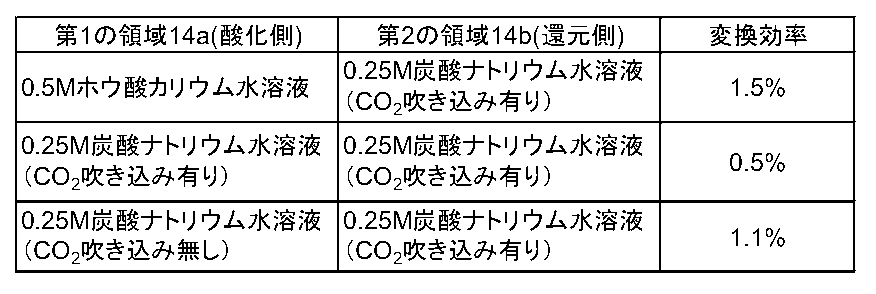
表2に示すように、第1の領域14aの電解液として二酸化炭素が吹き込まれていない0.25Mの炭酸ナトリウム水溶液を用いた場合の光から一酸化炭素への変換効率は、第1の領域14aの電解液として二酸化炭素が十分に吹き込まれた0.25Mの炭酸ナトリウム水溶液を用いた場合の光から一酸化炭素への変換効率よりも高かった。これは、第2の領域14bの電解液にのみ二酸化炭素を十分吹き込むことにより、第2の領域14bの電解液のpHが低下して第1の領域14aの電解液と第2の領域14bの電解液との間に液間電位差が生じるためである考えられる。また、第1の領域14aの電解液のpHが低下しないことにより、酸化電極層12による酸化反応の際の過電圧が抑制されるためであると考えられる。
このように、実施例の光電気化学反応装置では、例えば電解液を調製しなくてもCO2を吹き込むことにより、変換効率を向上させることができるため、酸化還元反応のサイクルを永続的に進行させることができる。
Claims (15)
- 電解液と、
前記電解液に浸漬された酸化電極層と、
前記電解液に浸漬された還元電極層と、
前記酸化電極層に電気的に接続された第1の面と、前記還元電極層に電気的に接続された第2の面とを有し、前記第1の面または前記第2の面に照射された光のエネルギーにより電荷分離を行う光起電力層と、を具備する光電気化学反応装置であって、
前記酸化電極層および前記還元電極層の少なくとも一つは細孔を含む多孔質構造を有する、光電気化学反応装置。 - 前記還元電極層は、
細孔を含む多孔質構造を有する導電層と、
前記導電層に積層され、微粒子状の還元触媒を含む還元触媒層と、を有する、請求項1に記載の光電気化学反応装置。 - 前記微粒子状の還元触媒は、5nm以下の粒子径を有する微粒子を全微粒子数の25%以上含む、請求項2に記載の光電気化学反応装置。
- 前記還元電極層は、
細孔を含む多孔質構造を有する導電層と、
前記導電層に積層され、還元触媒を含む多孔質構造を有する還元触媒層と、を有し、
前記還元触媒層は、300nm以上の幅を有する空隙を幅40マイクロメートルの範囲内に3つ以上有する、または100nm以上の幅を有する空隙を幅40マイクロメートルの範囲内に5つ以上有する、請求項1に記載の光電気化学反応装置。 - 前記還元触媒層は、前記還元触媒層の還元電位以下の最低電位と前記還元触媒層の酸化電位以上の最高電位とを有する高周波を印加することにより形成されたものである、請求項4に記載の光電気化学反応装置。
- 前記還元電極層は、界面活性剤を含む、請求項1に記載の光電気化学反応装置。
- 前記界面活性剤は、ポリビニルピロリドンまたはポリビニルアルコールを有する、請求項6に記載の光電気化学反応装置。
- 前記還元電極層は、イオン交換樹脂を含む、請求項1に記載の光電気化学反応装置。
- 前記酸化電極層は、前記光起電力層の前記第1の面に接し、且つ前記電解液の通過が可能である第1の貫通孔を有し、
前記還元電極層は、前記光起電力層の前記第2の面に接し、且つ前記電解液の通過が可能である第2の貫通孔を有し、
前記光起電力層は、前記電解液の通過が可能であり且つ前記第1の貫通孔および前記第2の貫通孔と連通する第3の貫通孔を有する、請求項1に記載の光電気化学反応装置。 - 前記第1の貫通孔ないし前記第3の貫通孔の少なくとも一つを閉塞するように設けられ、前記電解液に含まれる一部のイオンを透過するイオン交換膜をさらに具備する、請求項9に記載の光電気化学反応装置。
- 前記電解液に浸漬された撹拌器と、
前記電解液に接するように設けられ、前記電解液のpHを測定するpHセンサと、
前記電解液に接するように設けられた供給流路と、をさらに具備し、
前記pHセンサで測定した前記電解液のpHが基準範囲外であるとき、前記電解液のpHを調整する反応物質が前記供給流路を介して前記電解液に供給される、請求項1に記載の光電気化学反応装置。 - 前記電解液に浸漬され、前記還元電極層の対極としての機能を有する補助電極層をさらに具備する、請求項1に記載の光電気化学反応装置。
- 前記還元電極層および前記補助電極層に電気的に接続され、前記還元電極層と前記補助電極層との間に電位を印加する電源装置をさらに具備する、請求項12に記載の光電気化学反応装置。
- 前記還元電極層に印加される電位は、前記還元電極層の酸化電位よりも貴な電位の最高電位と、前記還元電極層の還元電位よりも卑な電位の最低電位と、を有する交流電位である、請求項13に記載の光電気化学反応装置。
- 前記電源装置に電気的に接続され、前記電源装置による電位の印加条件を制御する制御装置をさらに具備する、請求項13に記載の光電気化学反応装置。
Priority Applications (3)
| Application Number | Priority Date | Filing Date | Title |
|---|---|---|---|
| CN201580013278.5A CN106170586B (zh) | 2014-05-20 | 2015-05-20 | 光电化学反应装置 |
| EP15795869.5A EP3147385B1 (en) | 2014-05-20 | 2015-05-20 | Photoelectrochemical reaction device |
| US15/260,982 US10597787B2 (en) | 2014-05-20 | 2016-09-09 | Electrochemical reaction device |
Applications Claiming Priority (4)
| Application Number | Priority Date | Filing Date | Title |
|---|---|---|---|
| JP2014104621 | 2014-05-20 | ||
| JP2014-104621 | 2014-05-20 | ||
| JP2014-216315 | 2014-10-23 | ||
| JP2014216315 | 2014-10-23 |
Related Child Applications (1)
| Application Number | Title | Priority Date | Filing Date |
|---|---|---|---|
| US15/260,982 Continuation US10597787B2 (en) | 2014-05-20 | 2016-09-09 | Electrochemical reaction device |
Publications (1)
| Publication Number | Publication Date |
|---|---|
| WO2015178019A1 true WO2015178019A1 (ja) | 2015-11-26 |
Family
ID=54553700
Family Applications (1)
| Application Number | Title | Priority Date | Filing Date |
|---|---|---|---|
| PCT/JP2015/002527 Ceased WO2015178019A1 (ja) | 2014-05-20 | 2015-05-20 | 光電気化学反応装置 |
Country Status (4)
| Country | Link |
|---|---|
| US (1) | US10597787B2 (ja) |
| EP (1) | EP3147385B1 (ja) |
| CN (1) | CN106170586B (ja) |
| WO (1) | WO2015178019A1 (ja) |
Cited By (5)
| Publication number | Priority date | Publication date | Assignee | Title |
|---|---|---|---|---|
| JP2018154900A (ja) * | 2017-03-21 | 2018-10-04 | 株式会社東芝 | 電気化学反応装置と電気化学反応方法 |
| US10344388B2 (en) | 2015-09-16 | 2019-07-09 | Kabushiki Kaisha Toshiba | CO2 reduction catalyst, CO2 reduction electrode, CO2 reduction reaction apparatus, and process for producing CO2 reduction catalyst |
| WO2019181002A1 (ja) * | 2018-03-22 | 2019-09-26 | 株式会社 東芝 | 二酸化炭素電解装置および二酸化炭素電解方法 |
| WO2023042476A1 (ja) * | 2021-09-17 | 2023-03-23 | 株式会社日立製作所 | アノード光電極、アノード光電極の製造方法および水素製造設備 |
| JP2023152115A (ja) * | 2022-04-01 | 2023-10-16 | 株式会社カネカ | 光電解モジュール |
Families Citing this family (9)
| Publication number | Priority date | Publication date | Assignee | Title |
|---|---|---|---|---|
| JP6649293B2 (ja) * | 2017-01-25 | 2020-02-19 | 株式会社東芝 | 還元触媒、ならびにそれを用いた化学反応装置、還元方法、および還元物生産システム |
| JP6779849B2 (ja) * | 2017-09-19 | 2020-11-04 | 株式会社東芝 | 二酸化炭素の還元触媒体とその製造方法、還元電極、及び還元反応装置 |
| KR102187859B1 (ko) * | 2019-06-12 | 2020-12-08 | 한국과학기술연구원 | 이산화탄소 환원 및 에틸렌 생산용 염기성 전기촉매, 이를 포함하는 전극과 장치, 및 상기 전극의 제조방법 |
| WO2020257246A1 (en) * | 2019-06-17 | 2020-12-24 | The Regents Of The University Of Michigan | Co2 reduction into syngas |
| WO2021016539A2 (en) * | 2019-07-25 | 2021-01-28 | The Regents Of The University Of Michigan | Co2 conversion with nanowire-nanoparticle architecture |
| CN114207187B (zh) * | 2019-08-08 | 2024-08-02 | 奈诺普特科公司 | 辐射辅助电解槽单元和组 |
| JP7204619B2 (ja) * | 2019-09-17 | 2023-01-16 | 株式会社東芝 | 二酸化炭素電解装置及び二酸化炭素電解方法 |
| FR3125825B1 (fr) * | 2021-07-30 | 2024-03-01 | Totalenergies Se | Dispositif monolithique autonome de production d’hydrogène |
| TWI862232B (zh) * | 2023-10-20 | 2024-11-11 | 國立中央大學 | 半導體基板處理方法 |
Citations (7)
| Publication number | Priority date | Publication date | Assignee | Title |
|---|---|---|---|---|
| JPS6167790A (ja) * | 1984-09-11 | 1986-04-07 | Japan Storage Battery Co Ltd | イオン交換樹脂膜一電極接合体の製造法 |
| JP2005329376A (ja) * | 2004-05-21 | 2005-12-02 | Honda Motor Co Ltd | 電解水生成装置 |
| JP2006265697A (ja) * | 2005-03-25 | 2006-10-05 | Sharp Corp | 水分解用半導体光電極 |
| JP2010138039A (ja) * | 2008-12-12 | 2010-06-24 | Panasonic Corp | 炭素材料の精製方法および精製装置、ならびに非水電解質二次電池 |
| JP2011184767A (ja) * | 2010-03-10 | 2011-09-22 | Sharp Corp | 気体製造装置および気体製造方法 |
| JP2012112023A (ja) * | 2010-11-26 | 2012-06-14 | Sharp Corp | 気体製造装置および気体製造方法 |
| JP2012177160A (ja) * | 2011-02-25 | 2012-09-13 | Sharp Corp | 水素製造装置および水素製造方法 |
Family Cites Families (21)
| Publication number | Priority date | Publication date | Assignee | Title |
|---|---|---|---|---|
| US4160816A (en) | 1977-12-05 | 1979-07-10 | Rca Corporation | Process for storing solar energy in the form of an electrochemically generated compound |
| US4593129A (en) | 1984-04-18 | 1986-06-03 | Ethyl Corporation | Polyphosphazene process |
| JPH10290017A (ja) | 1997-04-14 | 1998-10-27 | Mitsubishi Heavy Ind Ltd | 光触媒 |
| GB0302654D0 (en) * | 2003-02-05 | 2003-03-12 | Univ Cambridge Tech | Processes of forming small diameter rods and tubes |
| US7605326B2 (en) * | 2003-11-24 | 2009-10-20 | Anderson Christopher M | Solar electrolysis power co-generation system |
| US20120222967A1 (en) * | 2004-02-24 | 2012-09-06 | Oakes Thomas W | System and Method for Generating Hydrogen Gas Using Renewable Energy |
| GB2414243A (en) * | 2004-03-15 | 2005-11-23 | Hydrogen Solar Ltd | Photoelectrochemical system |
| JP2009007647A (ja) * | 2007-06-29 | 2009-01-15 | Hitachi Ltd | 有機ハイドライド製造装置、及び、それを用いた分散電源と自動車 |
| CN102224279A (zh) * | 2008-10-08 | 2011-10-19 | 麻省理工学院 | 用于水电解和其它电化学技术的催化材料、光电阳极和光电化学电池 |
| CN101694816B (zh) * | 2009-10-16 | 2011-05-11 | 清华大学 | 一种异质结和光电化学混合太阳能电池 |
| JP5724170B2 (ja) | 2009-10-30 | 2015-05-27 | 株式会社豊田中央研究所 | 光化学反応デバイス |
| US20110114502A1 (en) | 2009-12-21 | 2011-05-19 | Emily Barton Cole | Reducing carbon dioxide to products |
| JP5663254B2 (ja) * | 2010-02-08 | 2015-02-04 | シャープ株式会社 | 水素製造装置および水素製造方法 |
| US8999119B2 (en) * | 2010-09-07 | 2015-04-07 | Panasonic Intellectual Property Management Co., Ltd. | Hydrogen production device |
| WO2012114787A1 (ja) | 2011-02-25 | 2012-08-30 | シャープ株式会社 | 水素製造装置および水素製造方法 |
| US20130168228A1 (en) * | 2011-04-12 | 2013-07-04 | Geoffrey A. Ozin | Photoactive Material Comprising Nanoparticles of at Least Two Photoactive Constituents |
| US9112217B2 (en) * | 2011-05-17 | 2015-08-18 | The Penn State University | Reverse electrodialysis supported microbial fuel cells and microbial electrolysis cells |
| DE102012205258A1 (de) * | 2012-03-30 | 2013-10-02 | Evonik Industries Ag | Photoelektrochemische Zelle, System und Verfahren zur lichtgetriebenen Erzeugung von Wasserstoff und Sauerstoff mit einer photoelektrochemischen Zelle und Verfahren zur Herstellung der photoelektrochemischen Zelle |
| US9947816B2 (en) * | 2012-04-03 | 2018-04-17 | California Institute Of Technology | Semiconductor structures for fuel generation |
| US9528192B1 (en) * | 2013-01-16 | 2016-12-27 | The United States Of America As Represented By The Administrator Of The National Aeronautics And Space Administration | Solar powered CO2 conversion |
| US20150259810A1 (en) * | 2014-03-17 | 2015-09-17 | California Institute Of Technology | Hydrogen evolution reaction catalysis |
-
2015
- 2015-05-20 WO PCT/JP2015/002527 patent/WO2015178019A1/ja not_active Ceased
- 2015-05-20 CN CN201580013278.5A patent/CN106170586B/zh not_active Expired - Fee Related
- 2015-05-20 EP EP15795869.5A patent/EP3147385B1/en active Active
-
2016
- 2016-09-09 US US15/260,982 patent/US10597787B2/en active Active
Patent Citations (7)
| Publication number | Priority date | Publication date | Assignee | Title |
|---|---|---|---|---|
| JPS6167790A (ja) * | 1984-09-11 | 1986-04-07 | Japan Storage Battery Co Ltd | イオン交換樹脂膜一電極接合体の製造法 |
| JP2005329376A (ja) * | 2004-05-21 | 2005-12-02 | Honda Motor Co Ltd | 電解水生成装置 |
| JP2006265697A (ja) * | 2005-03-25 | 2006-10-05 | Sharp Corp | 水分解用半導体光電極 |
| JP2010138039A (ja) * | 2008-12-12 | 2010-06-24 | Panasonic Corp | 炭素材料の精製方法および精製装置、ならびに非水電解質二次電池 |
| JP2011184767A (ja) * | 2010-03-10 | 2011-09-22 | Sharp Corp | 気体製造装置および気体製造方法 |
| JP2012112023A (ja) * | 2010-11-26 | 2012-06-14 | Sharp Corp | 気体製造装置および気体製造方法 |
| JP2012177160A (ja) * | 2011-02-25 | 2012-09-13 | Sharp Corp | 水素製造装置および水素製造方法 |
Non-Patent Citations (1)
| Title |
|---|
| See also references of EP3147385A4 * |
Cited By (9)
| Publication number | Priority date | Publication date | Assignee | Title |
|---|---|---|---|---|
| US10344388B2 (en) | 2015-09-16 | 2019-07-09 | Kabushiki Kaisha Toshiba | CO2 reduction catalyst, CO2 reduction electrode, CO2 reduction reaction apparatus, and process for producing CO2 reduction catalyst |
| JP2018154900A (ja) * | 2017-03-21 | 2018-10-04 | 株式会社東芝 | 電気化学反応装置と電気化学反応方法 |
| US10612147B2 (en) | 2017-03-21 | 2020-04-07 | Kabushiki Kaisha Toshiba | Electrochemical reaction device and electrochemical reaction method |
| WO2019181002A1 (ja) * | 2018-03-22 | 2019-09-26 | 株式会社 東芝 | 二酸化炭素電解装置および二酸化炭素電解方法 |
| JP2019167556A (ja) * | 2018-03-22 | 2019-10-03 | 株式会社東芝 | 二酸化炭素電解装置および二酸化炭素電解方法 |
| US11286573B2 (en) | 2018-03-22 | 2022-03-29 | Kabushiki Kaisha Toshiba | Carbon dioxide electrolytic device and method of electrolyzing carbon dioxide |
| WO2023042476A1 (ja) * | 2021-09-17 | 2023-03-23 | 株式会社日立製作所 | アノード光電極、アノード光電極の製造方法および水素製造設備 |
| JP2023152115A (ja) * | 2022-04-01 | 2023-10-16 | 株式会社カネカ | 光電解モジュール |
| JP7788336B2 (ja) | 2022-04-01 | 2025-12-18 | 株式会社カネカ | 光電解モジュール |
Also Published As
| Publication number | Publication date |
|---|---|
| EP3147385B1 (en) | 2020-02-19 |
| US10597787B2 (en) | 2020-03-24 |
| EP3147385A1 (en) | 2017-03-29 |
| CN106170586A (zh) | 2016-11-30 |
| EP3147385A4 (en) | 2017-11-08 |
| CN106170586B (zh) | 2018-10-19 |
| US20160376713A1 (en) | 2016-12-29 |
Similar Documents
| Publication | Publication Date | Title |
|---|---|---|
| WO2015178019A1 (ja) | 光電気化学反応装置 | |
| JP6672193B2 (ja) | 二酸化炭素の電解セルと電解装置 | |
| JP6744242B2 (ja) | 化学反応システム | |
| US20180073153A1 (en) | Optically transparent oxygen generation catalyst, production method thereof, and chemical reactor utilizing the same | |
| US10612146B2 (en) | Electrochemical reaction device | |
| US10472724B2 (en) | Chemical reaction device | |
| JP6495630B2 (ja) | 光電気化学反応装置 | |
| JP2020062639A (ja) | Co2還元触媒、co2還元電極、co2還元反応装置およびco2還元触媒の製造方法 | |
| JP2014101550A (ja) | 光化学反応システム | |
| JP2014101551A (ja) | 光化学反応装置 | |
| JP6768269B2 (ja) | 光電気化学反応装置 | |
| JP2017048442A (ja) | 光電気化学反応装置 | |
| US20170247804A1 (en) | Electrochemical reaction device and electrochemical reaction method | |
| TWI507566B (zh) | Photoelectrochemical reaction device | |
| WO2016088286A1 (ja) | 光電極とその製造方法、およびそれを用いた光電気化学反応装置 | |
| KR20150143854A (ko) | 광화학 반응 장치 및 박막 | |
| US20160369409A1 (en) | Photoelectrochemical reaction system | |
| JP2017155337A (ja) | 電気化学反応装置 | |
| JP2017155315A (ja) | 光電気化学反応装置 | |
| US20170029964A1 (en) | Method of forming composite catalyst layer, structure for electrochemical reaction device, and electrochemical reaction device | |
| JP6805307B2 (ja) | 化学反応装置の動作方法 | |
| JP6556887B2 (ja) | 光化学反応システム | |
| JP2017218679A (ja) | 化学反応装置およびその動作方法 |
Legal Events
| Date | Code | Title | Description |
|---|---|---|---|
| 121 | Ep: the epo has been informed by wipo that ep was designated in this application |
Ref document number: 15795869 Country of ref document: EP Kind code of ref document: A1 |
|
| REEP | Request for entry into the european phase |
Ref document number: 2015795869 Country of ref document: EP |
|
| WWE | Wipo information: entry into national phase |
Ref document number: 2015795869 Country of ref document: EP |
|
| NENP | Non-entry into the national phase |
Ref country code: DE |
|
| NENP | Non-entry into the national phase |
Ref country code: JP |