WO2015178258A1 - プリント配線板及びプリント配線板の製造方法 - Google Patents
プリント配線板及びプリント配線板の製造方法 Download PDFInfo
- Publication number
- WO2015178258A1 WO2015178258A1 PCT/JP2015/063679 JP2015063679W WO2015178258A1 WO 2015178258 A1 WO2015178258 A1 WO 2015178258A1 JP 2015063679 W JP2015063679 W JP 2015063679W WO 2015178258 A1 WO2015178258 A1 WO 2015178258A1
- Authority
- WO
- WIPO (PCT)
- Prior art keywords
- layer
- conductive layer
- base material
- wiring board
- printed wiring
- Prior art date
- Legal status (The legal status is an assumption and is not a legal conclusion. Google has not performed a legal analysis and makes no representation as to the accuracy of the status listed.)
- Ceased
Links
Images


Classifications
-
- H—ELECTRICITY
- H05—ELECTRIC TECHNIQUES NOT OTHERWISE PROVIDED FOR
- H05K—PRINTED CIRCUITS; CASINGS OR CONSTRUCTIONAL DETAILS OF ELECTRIC APPARATUS; MANUFACTURE OF ASSEMBLAGES OF ELECTRICAL COMPONENTS
- H05K1/00—Printed circuits
- H05K1/02—Details
- H05K1/11—Printed elements for providing electric connections to or between printed circuits
- H05K1/115—Via connections; Lands around holes or via connections
-
- H—ELECTRICITY
- H05—ELECTRIC TECHNIQUES NOT OTHERWISE PROVIDED FOR
- H05K—PRINTED CIRCUITS; CASINGS OR CONSTRUCTIONAL DETAILS OF ELECTRIC APPARATUS; MANUFACTURE OF ASSEMBLAGES OF ELECTRICAL COMPONENTS
- H05K1/00—Printed circuits
- H05K1/02—Details
- H05K1/03—Use of materials for the substrate
- H05K1/0313—Organic insulating material
- H05K1/032—Organic insulating material consisting of one material
- H05K1/034—Organic insulating material consisting of one material containing halogen
-
- H—ELECTRICITY
- H05—ELECTRIC TECHNIQUES NOT OTHERWISE PROVIDED FOR
- H05K—PRINTED CIRCUITS; CASINGS OR CONSTRUCTIONAL DETAILS OF ELECTRIC APPARATUS; MANUFACTURE OF ASSEMBLAGES OF ELECTRICAL COMPONENTS
- H05K1/00—Printed circuits
- H05K1/02—Details
- H05K1/09—Use of materials for the conductive, e.g. metallic pattern
-
- H—ELECTRICITY
- H05—ELECTRIC TECHNIQUES NOT OTHERWISE PROVIDED FOR
- H05K—PRINTED CIRCUITS; CASINGS OR CONSTRUCTIONAL DETAILS OF ELECTRIC APPARATUS; MANUFACTURE OF ASSEMBLAGES OF ELECTRICAL COMPONENTS
- H05K3/00—Apparatus or processes for manufacturing printed circuits
- H05K3/38—Improvement of the adhesion between the insulating substrate and the metal
- H05K3/381—Improvement of the adhesion between the insulating substrate and the metal by special treatment of the substrate
-
- H—ELECTRICITY
- H05—ELECTRIC TECHNIQUES NOT OTHERWISE PROVIDED FOR
- H05K—PRINTED CIRCUITS; CASINGS OR CONSTRUCTIONAL DETAILS OF ELECTRIC APPARATUS; MANUFACTURE OF ASSEMBLAGES OF ELECTRICAL COMPONENTS
- H05K3/00—Apparatus or processes for manufacturing printed circuits
- H05K3/40—Forming printed elements for providing electric connections to or between printed circuits
- H05K3/4038—Through-connections; Vertical interconnect access [VIA] connections
- H05K3/4084—Through-connections; Vertical interconnect access [VIA] connections by deforming at least one of the conductive layers
-
- H—ELECTRICITY
- H05—ELECTRIC TECHNIQUES NOT OTHERWISE PROVIDED FOR
- H05K—PRINTED CIRCUITS; CASINGS OR CONSTRUCTIONAL DETAILS OF ELECTRIC APPARATUS; MANUFACTURE OF ASSEMBLAGES OF ELECTRICAL COMPONENTS
- H05K3/00—Apparatus or processes for manufacturing printed circuits
- H05K3/46—Manufacturing multilayer circuits
- H05K3/4611—Manufacturing multilayer circuits by laminating two or more circuit boards
-
- H—ELECTRICITY
- H05—ELECTRIC TECHNIQUES NOT OTHERWISE PROVIDED FOR
- H05K—PRINTED CIRCUITS; CASINGS OR CONSTRUCTIONAL DETAILS OF ELECTRIC APPARATUS; MANUFACTURE OF ASSEMBLAGES OF ELECTRICAL COMPONENTS
- H05K3/00—Apparatus or processes for manufacturing printed circuits
- H05K3/46—Manufacturing multilayer circuits
- H05K3/4644—Manufacturing multilayer circuits by building the multilayer layer by layer, i.e. build-up multilayer circuits
- H05K3/4661—Adding a circuit layer by direct wet plating, e.g. electroless plating; insulating materials adapted therefor
-
- H—ELECTRICITY
- H05—ELECTRIC TECHNIQUES NOT OTHERWISE PROVIDED FOR
- H05K—PRINTED CIRCUITS; CASINGS OR CONSTRUCTIONAL DETAILS OF ELECTRIC APPARATUS; MANUFACTURE OF ASSEMBLAGES OF ELECTRICAL COMPONENTS
- H05K2201/00—Indexing scheme relating to printed circuits covered by H05K1/00
- H05K2201/09—Shape and layout
- H05K2201/09209—Shape and layout details of conductors
- H05K2201/095—Conductive through-holes or vias
- H05K2201/09509—Blind vias, i.e. vias having one side closed
-
- H—ELECTRICITY
- H05—ELECTRIC TECHNIQUES NOT OTHERWISE PROVIDED FOR
- H05K—PRINTED CIRCUITS; CASINGS OR CONSTRUCTIONAL DETAILS OF ELECTRIC APPARATUS; MANUFACTURE OF ASSEMBLAGES OF ELECTRICAL COMPONENTS
- H05K2203/00—Indexing scheme relating to apparatus or processes for manufacturing printed circuits covered by H05K3/00
- H05K2203/07—Treatments involving liquids, e.g. plating, rinsing
- H05K2203/0703—Plating
- H05K2203/072—Electroless plating, e.g. finish plating or initial plating
-
- H—ELECTRICITY
- H05—ELECTRIC TECHNIQUES NOT OTHERWISE PROVIDED FOR
- H05K—PRINTED CIRCUITS; CASINGS OR CONSTRUCTIONAL DETAILS OF ELECTRIC APPARATUS; MANUFACTURE OF ASSEMBLAGES OF ELECTRICAL COMPONENTS
- H05K3/00—Apparatus or processes for manufacturing printed circuits
- H05K3/40—Forming printed elements for providing electric connections to or between printed circuits
- H05K3/42—Plated through-holes or plated via connections
- H05K3/423—Plated through-holes or plated via connections characterised by electroplating method
-
- H—ELECTRICITY
- H05—ELECTRIC TECHNIQUES NOT OTHERWISE PROVIDED FOR
- H05K—PRINTED CIRCUITS; CASINGS OR CONSTRUCTIONAL DETAILS OF ELECTRIC APPARATUS; MANUFACTURE OF ASSEMBLAGES OF ELECTRICAL COMPONENTS
- H05K3/00—Apparatus or processes for manufacturing printed circuits
- H05K3/40—Forming printed elements for providing electric connections to or between printed circuits
- H05K3/42—Plated through-holes or plated via connections
- H05K3/429—Plated through-holes specially for multilayer circuits, e.g. having connections to inner circuit layers
Definitions
- the present invention relates to a printed wiring board and a method for manufacturing the printed wiring board.
- a main component of a base material for forming a conductive layer is a fluororesin having a small dielectric constant and dielectric loss tangent (see JP 2013-165171 A).
- a multilayer printed wiring board in which a plurality of conductive layers are formed is used.
- via holes (cylindrical conductors) connecting different conductive layers are formed.
- a method for forming such a via hole a method is used in which a hole is formed in a printed wiring board, an electroless plating is applied to the inner peripheral surface of the hole, and then a metal layer that connects two or more conductive layers is formed by electroplating. It has been known.
- a technique has been proposed in which a layer of conductive fine particles is formed on the inner peripheral surface of a hole in a printed wiring board and then electroless plating and electroplating are performed (see JP 2013-214785 A).
- the present invention has been made in view of the above inconveniences, and a printed wiring board in which conductive layers formed on both surfaces of a base material layer mainly composed of a fluororesin are reliably connected by via holes, and such printed wiring. It aims at providing the manufacturing method of a board.
- a printed wiring board which has been made to solve the above problems, includes a base material layer mainly composed of a fluororesin, and a first conductive layer laminated on one surface of the base material layer.
- it has a pretreated surface with a nitrogen atom content of 0.2 atomic% or more.
- formed in order to solve the said subject is the 1st laminated
- a method for manufacturing a printed wiring board comprising: a conductive layer; a second conductive layer laminated on the other surface of the base material layer; and a via hole that electrically connects the first conductive layer and the second conductive layer.
- the conductive layers formed on both surfaces of the base material layer mainly composed of fluororesin are reliably connected by via holes.
- the manufacturing method of the printed wiring board of this invention can connect the conductive layer formed in both surfaces of the base material layer which has a fluororesin as a main component by a via hole reliably.
- FIG. 1 is a schematic partial cross-sectional view showing a printed wiring board according to an embodiment of the present invention.
- 2A is a schematic partial cross-sectional view showing a manufacturing process of the printed wiring board of FIG. 2B is a schematic partial cross-sectional view showing the next manufacturing step of FIG. 2A for the printed wiring board of FIG. 1.
- 2C is a schematic partial cross-sectional view showing the next manufacturing step of FIG. 2B for the printed wiring board of FIG. 1.
- 2D is a schematic partial cross-sectional view showing the next manufacturing step of FIG. 2C for the printed wiring board of FIG. 1.
- FIG. 2E is a schematic partial cross-sectional view showing the next manufacturing step of FIG. 2D for the printed wiring board of FIG. 1.
- FIG. 1 is a schematic partial cross-sectional view showing a printed wiring board according to an embodiment of the present invention.
- 2A is a schematic partial cross-sectional view showing a manufacturing process of the printed wiring board of FIG. 2B is a schematic partial cross-section
- FIG. 3 is a schematic partial cross-sectional view showing a printed wiring board according to an embodiment different from FIG.
- FIG. 4A is a schematic partial cross-sectional view illustrating a manufacturing process of the printed wiring board of FIG. 4B is a schematic partial cross-sectional view showing the next manufacturing step of FIG. 4A for the printed wiring board of FIG. 3.
- FIG. 5 is a schematic partial cross-sectional view showing a printed wiring board according to an embodiment different from those in FIGS. 1 and 3.
- FIG. 6A is a schematic partial cross-sectional view illustrating a manufacturing process of the printed wiring board of FIG.
- FIG. 6B is a schematic partial cross-sectional view showing the next manufacturing step of FIG. 6A for the printed wiring board of FIG. 5.
- 6C is a schematic partial cross-sectional view showing the next manufacturing step of FIG. 6B for the printed wiring board of FIG. 5.
- 6D is a schematic partial cross-sectional view showing the next manufacturing step of FIG. 6C for the printed wiring board of FIG. 5.
- FIG. 6E is a schematic partial cross-sectional view showing the next manufacturing step of FIG. 6D for the printed wiring board of FIG. 5.
- FIG. 7 is a schematic partial cross-sectional view showing a printed wiring board according to an embodiment different from those in FIGS. 1, 3, and 5.
- FIG. 8 is a schematic partial cross-sectional view showing a printed wiring board according to an embodiment different from those shown in FIGS. 1, 3, 5, and 7.
- FIG. 9 is a schematic partial cross-sectional view showing a printed wiring board according to an embodiment different from those in FIGS. 1, 3, 5, 7, and 8.
- 10A is a schematic partial cross-sectional view showing a manufacturing process of the printed wiring board of FIG.
- FIG. 10B is a schematic partial cross-sectional view showing the next manufacturing step of FIG. 10A for the printed wiring board of FIG. 9.
- FIG. 10C is a schematic partial cross-sectional view showing the next manufacturing step of FIG. 10B for the printed wiring board of FIG. 9.
- FIG. 10D is a schematic partial cross-sectional view showing the next manufacturing step of FIG. 10C for the printed wiring board of FIG. 9.
- 10E is a schematic partial cross-sectional view showing the next manufacturing step of FIG. 10D for the printed wiring board of FIG. 9.
- FIG. 10F is a schematic partial cross-sectional view showing the next manufacturing step of FIG. 10E for the printed wiring board of FIG. 9.
- the printed wiring board according to one aspect of the present invention includes a base material layer mainly composed of a fluororesin, a first conductive layer laminated on one surface of the base material layer, and the other surface of the base material layer. Formed along a connection hole penetrating in the thickness direction through the second conductive layer, the base material layer, and at least one of the first conductive layer and the second conductive layer, and the first conductive layer and A printed wiring board including a via hole for electrically connecting the second conductive layer, wherein at least a part of the inner peripheral surface of the base material layer in the connection hole has an oxygen atom or nitrogen atom content of 0. It has a pretreatment surface of 2 atomic% or more.
- the printed wiring board is a pretreated surface that compensates for the low adhesion of a fluororesin having an oxygen atom or nitrogen atom content of 0.2 atomic% or more on at least a part of the inner peripheral surface of the base material layer in the connection hole Therefore, the pretreated surface exhibits high adhesion to the via hole.
- the printed wiring board can reliably connect the first conductive layer and the second conductive layer on both sides of the base material layer by via holes, and the pretreatment surface prevents the via holes from peeling off. Is expensive.
- the printed wiring board has a pre-processed surface, via holes can be easily stacked, and thus can be easily manufactured and provided at low cost.
- a modified layer having a hydrophilic organic functional group at least in the formation region of the pretreatment surface of the inner peripheral surface of the base material layer in the connection hole, adhesion between the base material layer and the via hole is achieved. This can further increase the manufacturing efficiency and reliability.
- the via hole may have a base conductor layer in contact with the inner peripheral surface of the connection hole and a main conductor layer in contact with the inner peripheral surface of the base conductor layer.
- the contact angle of the pretreated surface with pure water is preferably 90 ° or less.
- the peel strength between the via hole and the base material layer is preferably 1.0 N / cm or more.
- the via hole is peeled from the inner peripheral surface of the base material layer in the connection hole and the first conductive layer of the via hole resulting therefrom.
- peeling from the second conductive layer is prevented. Thereby, the connection between the first conductive layer and the second conductive layer becomes more reliable.
- a method for manufacturing a printed wiring board according to another aspect of the present invention includes a base material layer containing a fluororesin as a main component, a first conductive layer laminated on one surface of the base material layer, and the above-described base material.
- a method of manufacturing a printed wiring board comprising: a second conductive layer laminated on the other surface of the material layer; and a via hole that electrically connects the first conductive layer and the second conductive layer, the base layer And a step of forming a connection hole penetrating through at least one of the first conductive layer and the second conductive layer, and at least part of the inner peripheral surface of the base material layer in the connection hole, oxygen atoms or nitrogen atoms
- the method for producing the printed wiring board includes forming a pretreated surface having a content of oxygen atoms or nitrogen atoms of 0.2 atomic% or more on at least a part of the inner peripheral surface of the base material layer in the connection hole. Since the adhesion between the material layer and the via hole is improved, it is easy to form a via hole by laminating the base conductor layer and the main conductor layer, and the first conductive layer and the second conductive layer can be easily and reliably connected. . For this reason, the manufacturing method of the said printed wiring board enables provision of a cheap and reliable printed wiring board.
- the base conductor layer may be formed by adhesion of a conductive material or electroless plating of copper. In this way, by forming the base conductor layer by attaching a conductive material or by electroless plating of copper, the base conductor layer can be easily stacked and the main conductor layer can be reliably stacked. .
- “content ratio of oxygen atom or nitrogen atom” is, for example, X-ray photoelectron spectroscopy (ESCA: Electron Spectroscopy for Chemical Analysis or XPS: X-ray Photoelectron Spectroscopy), energy dispersive X-ray spectroscopy (EDXE) Dispersive X-ray Spectroscopy or EDS: Energy Dispersive X-ray Spectroscopy, Electron Probe Microanalysis Method (EPMA: Electron Probe Micro-Sm)pectrometry), secondary ion mass spectrometry (SIMS: Secondary Ion Mass Spectrometry), Auger electron spectroscopy (AES: Auger Electron Spectroscopy), can be measured by an electron microscope.
- EMA Electron Probe Micro-Sm
- SIMS Secondary Ion Mass Spectrometry
- Auger electron spectroscopy AES: Auger Electron Spectroscopy
- measurement is performed by scanning the surface with the X-ray source being an aluminum metal K alpha ray, a beam diameter of 50 ⁇ m, and an X-ray incident angle of 45 ° with respect to the analysis surface.
- the X-ray source being an aluminum metal K alpha ray, a beam diameter of 50 ⁇ m, and an X-ray incident angle of 45 ° with respect to the analysis surface.
- the measurement surface (such as a pretreatment surface) at the time of the measurement can be exposed by removing a conductor layer (metal or the like) covering the measurement surface by, for example, etching.
- the composition ratio of atoms at any depth position can be measured by the above method by sequentially removing the material in the direction perpendicular to the measurement surface by sputtering.
- the thickness of the surface treatment layer is measured with an electron microscope while analyzing the impurity concentration in the depth direction by SIMS etc. while removing by sputtering in a direction substantially parallel to the measurement surface.
- the content of oxygen atoms or nitrogen atoms on the surface can be measured by evaluating various combinations of the above methods.
- the “contact angle with pure water” is a value of a contact angle measured by the sessile drop method of JIS-R-3257 (1999).
- the “peel strength” is a value measured in accordance with JIS-K-6854-2 (1999) “Adhesive—Peeling peel strength test method—Part 2: 180 degree peel”.
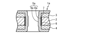
- a printed wiring board 1 in FIG. 1 includes a base material layer 2 mainly composed of a fluororesin, a first conductive layer 3 laminated on one surface of the base material layer 2, and the other base material layer 2.
- a second conductive layer 4 laminated on the surface, and a connection hole penetrating the base material layer 2, the first conductive layer 3 and the second conductive layer 4 in the thickness direction, and the first conductive layer 3 and A via hole 5 that electrically connects the second conductive layer 4 is mainly provided.
- the said base material layer 2 has the pre-processing surface 6 whose content rate of an oxygen atom or a nitrogen atom is 0.2 atomic% or more in the internal peripheral surface of the base material layer 2 in the said connection hole.
- the printed wiring board 1 further includes a modified layer 7 having a hydrophilic organic functional group in at least a region where the pretreatment surface 6 is formed on the inner peripheral surface of the base material layer.
- the base material layer 2 contains a fluororesin as a main component.
- the fluororesin is an organic group in which at least one hydrogen atom bonded to the carbon atom constituting the repeating unit of the polymer chain has a fluorine atom or a fluorine atom (hereinafter also referred to as “fluorine atom-containing group”). Refers to the substituted one.
- the fluorine atom-containing group is a group in which at least one hydrogen atom in a linear or branched organic group is substituted with a fluorine atom, and examples thereof include a fluoroalkyl group, a fluoroalkoxy group, and a fluoropolyether group. Can do.
- Fluoroalkyl group means an alkyl group in which at least one hydrogen atom is substituted with a fluorine atom, and includes a “perfluoroalkyl group”. Specifically, a “fluoroalkyl group” is a group in which all hydrogen atoms of an alkyl group are substituted with fluorine atoms, and all hydrogen atoms other than one hydrogen atom at the end of the alkyl group are substituted with fluorine atoms. Group.
- Fluoroalkoxy group means an alkoxy group in which at least one hydrogen atom is substituted with a fluorine atom, and includes a “perfluoroalkoxy group”. Specifically, a “fluoroalkoxy group” is a group in which all hydrogen atoms of an alkoxy group are substituted with fluorine atoms, and all hydrogen atoms other than one hydrogen atom at the end of the alkoxy group are substituted with fluorine atoms. Group.
- the “fluoropolyether group” is a monovalent group having an oxyalkylene unit as a repeating unit and having an alkyl group or a hydrogen atom at the terminal, and at least one hydrogen of the alkylene oxide chain or the terminal alkyl group A monovalent group in which an atom is substituted with a fluorine atom.
- the “fluoropolyether group” includes a “perfluoropolyether group” having a plurality of perfluoroalkylene oxide chains as repeating units.
- fluororesin constituting the base layer 2 examples include polytetrafluoroethylene (PTFE), polytetrafluoroethylene / perfluoroalkyl vinyl ether copolymer (PFA), and tetrafluoroethylene / hexafluoropropylene copolymer (FEP).
- PTFE polytetrafluoroethylene
- PFA polytetrafluoroethylene / perfluoroalkyl vinyl ether copolymer
- FEP tetrafluoroethylene / hexafluoropropylene copolymer
- Tetrafluoroethylene / ethylene copolymer ETFE
- PVDF polyvinylidene fluoride
- PCTFE polychlorotrifluoroethylene
- ECTFE chlorotrifluoroethylene / ethylene copolymer
- PVF polyvinyl fluoride
- a thermoplastic fluororesin (THV) and a fluoroelastomer composed of three types of monomers such as tetrafluoroethylene, hexafluoropropylene, and vinylidene fluoride can be exemplified.
- a mixture or copolymer containing these compounds can also be used as a material constituting the base layer 2.
- the fluororesin constituting the substrate layer 2 tetrafluoroethylene / hexapropylene copolymer (FEP), polytetrafluoroethylene / perfluoroalkyl vinyl ether copolymer (PFA), or polytetrafluoroethylene (PTFE) is preferred.
- FEP tetrafluoroethylene / hexapropylene copolymer
- PFA polytetrafluoroethylene / perfluoroalkyl vinyl ether copolymer
- PTFE polytetrafluoroethylene
- the base material layer 2 includes, as optional components, for example, engineering plastics, flame retardants, flame retardant aids, pigments, antioxidants, reflection imparting agents, masking agents, lubricants, processing stabilizers, plasticizers, foaming agents, and the like. May be included.
- the engineering plastic can be selected from known materials such as polyacetal, polyamide, polycarbonate, modified polyphenylene ether, polybutylene terephthalate, and liquid crystal polymer according to the characteristics required for the base material layer 2, and typically Aromatic polyetherketone resins can be used.
- This aromatic polyetherketone has a structure in which the benzene rings are bonded to the para position and the benzene rings are connected by a rigid ketone bond (—C ( ⁇ O) —) or a flexible ether bond (—O—). It is a thermoplastic resin.
- aromatic polyether ketone for example, ether ether, benzene ring, ether bond, benzene ring, ketone bond, and polyether ether ketone (PEEK) having a structural unit in which the benzene ring is arranged in this order, ether bond, benzene ring And polyether ketone (PEK) having a structural unit in which a ketone bond and a benzene ring are arranged in this order.
- PEEK is preferable as the aromatic polyether ketone.
- Such an aromatic polyether ketone is excellent in wear resistance, heat resistance, insulation, workability and the like.
- aromatic polyether ketones such as PEEK.
- aromatic polyether ketones those of various grades are commercially available, and a single grade of aromatic polyether ketone that is commercially available may be used alone, or multiple grades of aromatic polyether ketone.
- a ketone may be used in combination, or a modified aromatic polyether ketone may be used.
- the lower limit of the ratio of the total content of engineering plastics in the base material layer 2 to the fluororesin is not particularly limited, but is preferably 10% by mass, more preferably 20% by mass, and even more preferably 35% by mass.
- the upper limit of the ratio of the total content of engineering plastics to the fluororesin is not particularly limited, but is preferably 50% by mass and more preferably 45% by mass.
- the flame retardant various known ones can be used, and examples thereof include halogen flame retardants such as bromine flame retardants and chlorine flame retardants.
- flame retardant aid various known ones can be used, and examples thereof include antimony trioxide.
- pigment various known pigments can be used, and examples thereof include titanium oxide.
- antioxidant various known ones can be used, and examples thereof include a phenolic antioxidant.
- reflection imparting agent various known ones can be used, and examples thereof include titanium oxide.
- the base material layer 2 may be provided with a hollow structure.
- the lower limit of the average thickness of the base material layer 2 is preferably 3 ⁇ m, and more preferably 6 ⁇ m.
- an upper limit of the average thickness of the base material layer 2 100 micrometers is preferable and 55 micrometers is more preferable.
- the average thickness of the base material layer 2 is less than the said minimum, there exists a possibility that the intensity
- the average thickness of the base material layer 2 exceeds the said upper limit, there exists a possibility that the flexibility of the base material layer 2 and the said printed wiring board 1 may become inadequate.
- the pretreatment surface 6 is formed by surface treatment on the surface of the base material layer 2 (inner peripheral surface of the connection hole), and contains oxygen atoms or nitrogen atoms.
- the pretreatment surface 6 is a surface having an atomic composition different from the inside of the base material layer 2.
- the pretreatment surface 6 is formed on the entire inner peripheral surface of the base material layer in the connection hole.
- the lower limit of the oxygen atom or nitrogen atom content of the pretreated surface 6 is 0.2 atomic%, preferably 1 atomic%, and more preferably 5 atomic%.
- the upper limit of the content of oxygen atoms or nitrogen atoms on the pretreated surface 6 is preferably 30 atomic%, and more preferably 20 atomic%.
- the adhesion of the pretreatment surface 6 to the via hole 5 is not limited to the case where the via hole 5 is directly laminated on the pretreatment surface 6 but the via hole 5 is laminated on the pretreatment surface 6 via the modified layer 7. Also in this case, it means that the via hole 5 is difficult to peel off.
- the upper limit of the contact angle of the pretreated surface 6 with respect to pure water is preferably 90 °, more preferably 80 °.
- the lower limit of the contact angle of the pretreated surface 6 with respect to pure water is not particularly limited.
- the contact angle with respect to pure water can be measured using a contact angle measuring instrument “GI-1000” manufactured by ERMA.
- the lower limit of the wetting tension of the pretreated surface 6 is preferably 50 mN / m, more preferably 60 mN / m. When the wetting tension of the pretreated surface 6 is less than the lower limit, the adhesion between the pretreated surface 6 and the via hole 5 is insufficient, and the via hole 5 may be peeled off.
- the lower limit of the wetting tension is larger than that of pure polytetrafluoroethylene (PTFE). That is, the surface of the base material layer 2 has higher surface adhesion than the ordinary fluororesin by forming the pretreatment surface 6.
- the first conductive layer 3 and the second conductive layer 4 are layers formed of a conductor such as a metal, and each have a planar shape including a wiring for an electric circuit, a land for mounting an electric component, and the like.
- the planar shapes of the first conductive layer 3 and the second conductive layer 4 are formed, for example, by etching a conductor laminated on the base material layer 2.
- the material for forming the first conductive layer 3 and the second conductive layer 4 may be any material as long as it has conductivity.
- the material is copper, stainless steel, aluminum, nickel or the like, typically copper. It is formed.
- the lower limit of the average thickness of the first conductive layer 3 and the second conductive layer 4 is preferably 0.01 ⁇ m, and more preferably 0.1 ⁇ m.
- the upper limit of the average thickness of the first conductive layer 3 and the second conductive layer 4 is preferably 100 ⁇ m, and more preferably 20 ⁇ m.
- the via hole 5 includes an inner peripheral surface of the connection hole in which the modified layer 7 is formed (an inner peripheral surface of the modified layer 7), an end surface in the connection hole of the first conductive layer 3 and the second conductive layer 4 (connection hole). Inner peripheral surface), the connection hole vicinity region of the outer surface of the first conductive layer 3 (surface opposite to the base material layer 2), and the outer surface of the second conductive layer 4 (surface opposite to the base material layer 2). ) And the base conductor layer 8 stacked so as to be in contact with the region near the connection hole, and the main conductor layer stacked so as to be in contact with the inner peripheral surface and the outer surface (surface far from the base material layer 2) of the base conductor layer 8. 9.
- the lower limit of the peel strength between the via hole 5 and the base material layer 2 is preferably 1.0 N / cm, more preferably 1.5 N / cm, and further preferably 2.0 N / cm.
- the upper limit of the peel strength between the via hole 5 and the base material layer 2 is not particularly limited. When the peel strength between the via hole 5 and the base material layer 2 is less than the above lower limit, the via hole 5 is peeled from the base material layer 2 to peel off the connecting portion with the first conductive layer 3 or the second conductive layer 4. May cause tearing.
- the base conductor layer 8 is a thin layer having conductivity, and is used as an adherend when the main conductor layer 9 is formed by electroplating.
- the underlying conductor layer 8 is formed of a metal laminated by electroless plating. Examples of the metal that forms the underlying conductor layer 8 include metals such as copper, silver, nickel, and palladium. Among them, flexibility, thickness, adhesion with electrolytic copper plating are good, and low electrical resistance is achieved. Copper is preferred.
- the lower limit of the average thickness of the base conductor layer 8 is preferably 0.01 ⁇ m, and more preferably 0.2 ⁇ m.
- the upper limit of the average thickness of the underlying conductor layer 8 is preferably 1 ⁇ m, and more preferably 0.5 ⁇ m. If the average thickness of the underlying conductor layer 8 is less than the lower limit, the continuity of the underlying conductor layer 8 cannot be ensured, and the main conductor layer 9 may not be formed uniformly. Further, when the average thickness of the underlying conductor layer 8 exceeds the above upper limit, there is a possibility that the cost may be unnecessarily increased.
- the main conductor layer 9 is formed of a metal such as copper or nickel laminated on the base conductor layer 8 by electroplating. By providing the main conductor layer 9 on the inner peripheral surface after forming the base conductor layer 8 in this manner, the via hole 5 having excellent conductivity can be easily and reliably formed.
- the lower limit of the average thickness of the main conductor layer 9 is preferably 1 ⁇ m and more preferably 5 ⁇ m.
- the upper limit of the average thickness of the main conductor layer 9 is preferably 50 ⁇ m and more preferably 30 ⁇ m.
- the modified layer 7 has a hydrophilic organic functional group that easily binds to a metal or the like in at least a region where the pretreatment surface 6 is formed in the inner peripheral surface of the substrate layer 2 in the connection hole.
- the adhesion between the base conductor layer 8 and the base conductor layer 8 is further improved.
- the modified layer 7 preferably contains a siloxane bond (Si—O—Si). That is, the modifying layer 7 is formed by bonding a modifying agent (silane coupling agent) having a hydrophilic organic functional group and generating a siloxane bond to the fluororesin that is the main component of the base material layer 2. It is preferable.
- the hydrophilic organic functional group is bonded to Si atoms constituting the siloxane bond. This hydrophilic organic functional group imparts wettability to the surface side of the base material layer 2.
- the chemical bond between the fluororesin and the modifier may be composed of only a covalent bond or may include a covalent bond and a hydrogen bond.
- the modified layer 7 is a region that is considered to have a different microstructure, molecular structure, and abundance of elements from the region excluding the modified layer 7 in the vicinity of the surface of the base material layer 2.
- the modified layer 7 has a hydrophilic organic functional group
- the base material layer 2 becomes hydrophilic and the wettability of the surface is improved.
- the processing speed and the uniformity of the surface treatment can be improved. .
- Si atoms constituting the siloxane bond include at least one of N atom, C atom, O atom, and S atom. And covalently bonded to the C atom of the base material layer 2.
- the Si atom of the siloxane bond includes —O—, —S—, —SS—, — (CH 2 ) n—, —NH—, — (CH 2 ) n—NH—, — (CH 2 ). It is bonded to the C atom of the fluororesin through an atomic group such as n—O— (CH 2 ) m— (n and m are integers of 1 or more).
- hydrophilic organic functional group a hydroxyl group, carboxy group, carbonyl group, amino group, amide group, sulfide group, sulfonyl group, sulfo group, sulfonyldioxy group, epoxy group, methacryl group and mercapto group are preferable. Among these, those containing N atoms or S atoms are more preferable.
- These hydrophilic organic functional groups further improve the adhesion of the surface of the base material layer 2.
- the modified layer 7 may contain two or more of these hydrophilic organic functional groups. Thus, by imparting hydrophilic organic functional groups having different properties to the modified layer 7, the surface reactivity of the base material layer 2 can be varied.
- These hydrophilic organic functional groups are bonded to Si atoms, which are constituents of siloxane bonds, directly or via one or more C atoms (for example, a methylene group or a phenylene group).
- a silane coupling agent having a hydrophilic organic functional group in the molecule is suitable, and among them, a hydrolyzable silicon containing Si atom is contained. Those having a functional group are more preferred.
- Such a silane coupling agent is chemically bonded to the fluororesin constituting the base material layer 2.
- the chemical bond between the silane coupling agent and the fluororesin of the base material layer 2 may be composed of only a covalent bond or may include a covalent bond and a hydrogen bond.
- the “hydrolyzable silicon-containing functional group” refers to a group capable of forming a silanol group (Si—OH) by hydrolysis.
- the upper limit of the contact angle with the pure water on the surface of the modified layer 7 is 90 °, preferably 80 °, and more preferably 70 °.
- the adhesive strength with an adhesive such as a conductive pattern may be insufficient.
- the lower limit of the contact angle with the pure water on the surface of the modified layer 7 is not particularly limited.
- the modified layer 7 has the following etching resistance, that is, an etching solution containing iron chloride, having a specific gravity of 1.33 g / cm 3 and a free hydrochloric acid concentration of 0.2 mol / L. It is preferable that the modified layer 7 is not removed with respect to the etching treatment that is used for immersion at 45 ° C. for 2 minutes.
- “the modified layer 7 is not removed” means that hydrophilicity is not lost, and that the contact angle with pure water does not exceed 90 ° in the portion where the modified layer 7 is provided.
- the etching treatment may cause a minute portion having hydrophobicity in the region where the modified layer 7 is formed to be patchy. However, if the entire region has hydrophilicity, such a state may be hydrophilic. It is assumed that sex is maintained.
- the modified layer 7 has etching resistance to an etching solution containing copper chloride.
- the modified layer 7 has the etching resistance with respect to the iron chloride-containing etching solution, it is confirmed that the modified layer 7 has the etching resistance with respect to the copper chloride-containing etching solution. ing.
- the lower limit of the adhesion energy between the surface of the modified layer 7 and water is preferably 50 dyne / cm.
- the adhesion energy between the surface of the modified layer 7 and water is less than the lower limit, the adhesion of the surface of the base material layer 2 may be insufficient in comparison with pure polytetrafluoroethylene (PTFE). .
- the lower limit of the wetting tension on the surface of the modified layer 7 is preferably 50 mN / m, more preferably 60 mN / m. If the wetting tension is less than the above lower limit, the adhesion is insufficient, and the adhesive may be peeled off from the modified layer 7. Since the lower limit of the wetting tension is larger than the wetting tension of pure polytetrafluoroethylene (PTFE), the surface of the modified layer 7 has improved adhesion. On the other hand, when the wetting tension on the surface of the modified layer 7 is less than the lower limit, the adhesion of the surface of the modified layer 7 may be insufficient.
- the “wetting tension” is a value measured according to JIS-K-6768 (1999).
- the lower limit of the peel strength of the epoxy resin adhesive having an average thickness of 25 ⁇ m with respect to the surface of the modified layer 7 measured using a polyimide sheet having an average thickness of 12.5 ⁇ m as the flexible adherend is preferably 1.0 N / cm. 3.0 N / cm is more preferable, and 5.0 N / cm is more preferable.
- the peel strength of the epoxy resin adhesive with respect to the surface of the modified layer 7 is less than the lower limit, the adhesion of the via hole 5 to the modified layer 7 may not be sufficiently improved.
- the lower limit of the average thickness of the modified layer 7 is not particularly limited, but is preferably 10 nm, and more preferably 50 nm.
- the upper limit of the average thickness of the modified layer 7 is preferably 400 nm, and more preferably 200 nm.
- the transmission loss may be increased because the dielectric constant ( ⁇ ) and the dielectric loss tangent (tan ⁇ ) of the modified layer 7 are larger than those of the fluororesin. .
- the average thickness of the modified layer 7 can be measured using an optical interference type film thickness measuring machine, an X-ray photoelectron spectroscopy (X-ray photoelectron spectroscopy) analyzer, an electron microscope, or the like.
- the upper limit of the average surface roughness Ra of the inner peripheral surface of the modified layer 7 is preferably 4 ⁇ m, more preferably 2 ⁇ m, and even more preferably 1 ⁇ m.
- the “average surface roughness Ra” means an arithmetic average roughness measured in accordance with JIS-B-0601 (2013).
- the modified layer 7 is preferably formed after the pretreatment surface 6 is formed at least on the inner peripheral surface of the connection hole formed in the base material layer 2. Since the base layer 2 is formed with the pretreatment surface 6 so that the adhesion of the end face is improved, the formation of the modified layer 7 is facilitated, and the adhesion of the via hole 5 is further improved.
- the method for manufacturing the printed wiring board 1 includes a step of preparing a laminate having a base material layer 2, a first conductive layer 3, and a second conductive layer 4 (a laminate preparation step), and forming connection holes in the laminate.
- a step of forming a pretreatment surface 6 having a content of oxygen atoms or nitrogen atoms of 0.2 atomic% or more on the inner peripheral surface of the base material layer 2 in the formed connection hole Treatment surface formation step
- a step of forming a modified layer 7 having a hydrophilic organic functional group in a formation region of at least the pretreatment surface 6 in the inner peripheral surface of the connection hole (a modification layer formation step)
- the first conductive layer 3 and the second conductive layer 4 are etched to form a conductive pattern. And a degree.
- ⁇ Laminated body preparation process> a laminate having the base material layer 2, the first conductive layer 3, and the second conductive layer 4 as shown in FIG. 2A is prepared.
- a method of laminating the conductor for forming the first conductive layer 3 and the second conductive layer 4 on the base material layer 2 for example, a method of attaching a metal foil with an adhesive or the like, A method of vapor deposition is applied.
- connection hole forming process As shown in FIG. 2B, a connection hole penetrating the base material layer 2, the first conductive layer 3, and the second conductive layer 4 is formed in the laminate.
- connection hole As a method for forming such a connection hole, a known method such as punching, laser processing, or drilling can be applied.
- Pretreatment surface formation process At least the end surface of the base material layer 2 (the inner peripheral surface of the connection hole) is surface-treated, so that oxygen atoms or nitrogen atoms are formed on the end surface of the base material layer 2 as shown in FIG.
- the pretreatment surface 6 containing is formed.
- Examples of the surface treatment include Na etching, alkali treatment, plasma treatment, and radiation irradiation.
- the molecules on the end face of the base material layer 2 are finely cut or removed (etched), whereby oxygen atoms and nitrogen atoms can be added.
- the Na etching is a process of etching the surface layer of the fluororesin on the end face of the base material layer 2 by immersing the base material layer 2 in an etching solution containing metal Na such as “Tetra Etch” manufactured by Junko Co., Ltd.
- the alkali treatment is a treatment for etching the surface layer of the fluororesin on the end face of the base material layer 2 by immersing the base material layer 2 in a strong alkali solution such as potassium hydroxide.
- the plasma treatment is a treatment of etching the surface layer of the fluororesin on the end face of the base material layer 2 by bringing the base material layer 2 into contact with plasma.
- plasma gas such as oxygen, nitrogen, hydrogen, argon, ammonia
- the plasma treatment may be performed using plasma of an inert gas containing a compound having a hydrophilic group.
- the radiation irradiation is performed by irradiating the end surface of the base material layer 2 with high-energy radiation to extract fluorine atoms of the fluororesin on the end surface of the base material layer 2, so that oxygen atoms or nitrogen atoms are substituted for the fluorine atoms. It is a process to add.
- the radiation applied to the base material layer 2 include an electron beam and an electromagnetic wave.
- a coupling agent having a hydrophilic organic functional group and capable of binding to the fluororesin is applied to at least the formation region of the pretreatment surface 6 on the end surface of the base material layer 2, so that FIG.
- a modified layer 7 in contact with the pretreatment surface 6 is formed.
- the modified layer 7 is formed by bonding a coupling agent to the fluororesin of the base material layer 2.
- the chemical bond between the fluororesin of the base material layer 2 and the coupling agent may be constituted only by a covalent bond or may contain a covalent bond and a hydrogen bond.
- the coupling agent having such a hydrophilic organic functional group and bonded to the fluororesin examples include a silane coupling agent and a titanium coupling agent, and particularly forms a siloxane bond (Si—O—Si).
- Silane coupling agents are preferred, and silane coupling agents having hydrolyzable functional groups containing Si atoms are more preferred. That is, the preferable modified layer 7 includes a siloxane bond.
- the hydrophilic organic functional group is directly on the Si atom which is a constituent element of the siloxane bond, or one or a plurality of C atoms (for example, a methylene group or a phenylene group). Join through.
- Si atoms constituting the siloxane bond include at least one of N, C, O, and S atoms. And covalently bonded to the C atom of the base material layer 2.
- the Si atom of the siloxane bond includes —O—, —S—, —SS—, — (CH 2 ) n—, —NH—, — (CH 2 ) n—NH—, — (CH 2 ). It is bonded to the C atom of the fluororesin through an atomic group such as n—O— (CH 2 ) m— (n and m are integers of 1 or more).
- the hydrolyzable functional group containing the Si atom is specifically a group in which an alkoxy group is bonded to the Si atom.
- alkoxy group include methoxy group, ethoxy group, propoxy group, t-butoxy group, pentyloxy group and the like.
- hydrophilic organic functional group containing an N atom examples include an amino group and a ureido group.
- silane coupling agent having a hydrophilic organic functional group containing an N atom examples include aminoalkoxysilane, ureidoalkoxysilane, and derivatives thereof.
- aminoalkoxysilane examples include 3-aminopropyltrimethoxysilane, 3-aminopropyltriethoxysilane, N- (2-aminoethyl) -3-aminopropylmethyldimethoxysilane, and N- (2-aminoethyl) -3.
- aminoalkoxysilane derivatives include ketimines such as 3-triethoxysilyl-N- (1,3-dimethyl-butylidene) propylamine, and N-vinylbenzyl-2-aminoethyl-3-aminopropyltrimethoxysilane acetic acid.
- ketimines such as 3-triethoxysilyl-N- (1,3-dimethyl-butylidene) propylamine
- N-vinylbenzyl-2-aminoethyl-3-aminopropyltrimethoxysilane acetic acid examples include salts of silane coupling agents such as salts.
- ureidoalkoxysilane examples include 3-ureidopropyltriethoxysilane, 3-ureidopropyltrimethoxysilane, N- (2-ureidoethyl) -3-aminopropyltrimethoxysilane, and the like.
- hydrophilic organic functional group containing an S atom examples include a mercapto group and a sulfide group.
- silane coupling agent having a hydrophilic organic functional group containing an S atom examples include mercaptoalkoxysilane, sulfide alkoxysilane, and derivatives thereof.
- Examples of the mercaptoalkoxysilane include 3-mercaptopropyltrimethoxysilane, 3-mercaptopropyltriethoxysilane, 3-mercaptopropyl (dimethoxy) methylsilane, and the like.
- sulfide alkoxysilane examples include bis (3-triethoxysilylpropyl) tetrasulfide and bis (3-triethoxysilylpropyl) disulfide.
- the silane coupling agent may be one introduced with a modifying group.
- a modifying group a phenyl group is preferable.
- silane coupling agents include 3-aminopropyltriethoxysilane, N-phenyl-3-aminopropyltrimethoxysilane, 3-ureidopropyltriethoxysilane, 3-mercaptopropyltrimethoxysilane, or bis (among others).
- 3-Triethoxysilylpropyl) tetrasulfide is preferred.
- titanium coupling agent for forming the modified layer 7 examples include isopropyl triisostearoyl titanate, isopropyl tristearoyl titanate, isopropyl trioctanoyl titanate, isopropyl dimethacrylisostearoyl titanate, isopropyl tridodecylbenzenesulfonyl titanate, Isopropyl isostearoyl diacryl titanate, isopropyl tri (dioctyl phosphate) titanate, isopropyl tricumyl phenyl titanate, isopropyl tris (dioctyl pyrophosphate) titanate, isopropyl tri (N-aminoethyl-aminoethyl) titanate, tetraisopropyl bis (dioctyl phosphite) ) Titanate, tetraoctylbis (ditridecylpho
- the via hole forming step includes a step of laminating the base conductor layer 8 so as to be in contact with the inner peripheral surface of the connection hole in which the modified layer 7 is formed (base conductor layer laminating step), and a main conductor so as to be in contact with the surface of the base conductor layer 8.
- a step of forming the layer 9 main conductor layer forming step).
- the inner peripheral surface of the modified layer 7, the end surface and the outer surface of the first conductive layer 3, and the end surface and the outer surface of the second conductive layer 4 are formed by electroless plating.
- a base conductor layer 8 in contact with is formed.
- Electroless plating is a treatment for depositing a metal having catalytic activity by the reducing action of the catalyst, and various commercially available electroless plating solutions can be used.
- the main conductor layer 9 in contact with the inner peripheral surface of the base conductor layer 8 is formed by laminating a metal by electroplating using the base conductor layer 8 as an adherend, thereby forming the main conductor layer 9 shown in FIG. A via hole 5 of the printed wiring board 1 is formed.
- the conductive pattern is formed by etching the first conductive layer 3 and the second conductive layer 4 by a known etching method for forming a resist pattern by photolithography, for example.
- the printed wiring board 1 becomes hydrophilic because it has a pretreated surface 6 containing 0.2 atomic% or more of oxygen atoms or nitrogen atoms on the end surface where the base material layer 2 is formed by the connection holes, and wettability with liquid. Therefore, the surface chemical reaction in the liquid processing step such as plating for forming the base conductor layer 8 is promoted. For this reason, the adhesiveness of the base conductor layer 8 and the via hole 5 to the end face of the base material layer 2 is high. Adhesion is further improved by laminating a modified layer 7 having a hydrophilic organic functional group on the pretreated surface 6. Thereby, the printed wiring board 1 has high reliability of electrical connection between the first conductive layer 3 and the second conductive layer 4.
- the via hole 5 can be easily and reliably formed by laminating the main conductor layer 9 having a low electric resistance by electroplating. For this reason, the printed wiring board 1 can be provided at a relatively low cost.
- the printed wiring board 1 is formed by forming a modified layer 7 using a silane coupling agent, so that a hydrophilic organic functional group that improves the adhesion of the via hole 5 and a fluororesin of the base material layer 2 are mixed with silicon. It can be efficiently bonded through a siloxane bond as a skeleton. Thereby, the printed wiring board 1 is excellent in productivity and reliability.
- the coupling agent has a high binding property to the end surface of the base material layer 2. For this reason, it is easy to form the modified layer 7 on the end face of the base material layer 2, and the formation efficiency of the via hole 5 and the reliability of the printed wiring board can be further improved.
- the printed wiring board 1a of FIG. 3 includes a base material layer 2 mainly composed of a fluororesin, a first conductive layer 3 laminated on one surface of the base material layer 2, and the other of the base material layer 2.
- the said base material layer 2 has the pre-processing surface 6 whose content rate of an oxygen atom or a nitrogen atom is 0.2 atomic% or more in the internal peripheral surface of the base material layer 2 in the said connection hole.
- the printed wiring board 1a has a modified layer 7 laminated on the inner peripheral surface of the connection hole so as to be in contact with the pretreatment surface 6 and having a hydrophilic organic functional group.
- the via hole 5a of the printed wiring board 1a includes a base conductor layer 8a laminated so as to be in contact with the inner peripheral surface of the connection hole in which the modified layer 7 is formed (the inner peripheral surface of the modified layer 7), and the base conductor layer 8a.
- the base conductor layer 8a of the printed wiring board 1a of FIG. 3 is a thin layer formed by attaching a conductive material, and is used as an adherend when forming the main conductor layer 9a.
- Such a base conductor layer 8a can be formed by various commercially available processing agents.
- Examples of the conductive material for forming the underlying conductor layer 8a include conductive fine particles such as carbon and metal, and among these, carbon fine particles and palladium fine particles are preferable. Such adhesion of the conductive material can be performed, for example, by applying a fine particle dispersion in which conductive fine particles are dispersed in a liquid.
- the lower limit of the average thickness of the base conductor layer 8a is preferably 0.01 ⁇ m, more preferably 0.1 ⁇ m.
- the upper limit of the average thickness of the underlying conductor layer 8a is preferably 0.5 ⁇ m, and more preferably 0.2 ⁇ m. If the average thickness of the underlying conductor layer 8a is less than the lower limit, the continuity of the underlying conductor layer 8a cannot be ensured, and the main conductor layer 9a may not be formed uniformly. Further, when the average thickness of the underlying conductor layer 8a exceeds the above upper limit, the diameter of the via hole 5a increases, so that the degree of integration of the printed wiring board may be reduced.
- the main conductor layer 9a of the printed wiring board 1a in FIG. 3 is formed on the inner peripheral surface of the base conductor layer 8a, the end surface in the connection hole of the first conductive layer 3 and the second conductive layer 4, and the outer surface of the first conductive layer 3. It is formed of a metal laminated by electroplating in the region near the connection hole and in the region near the connection hole on the outer surface of the second conductive layer 4. About the metal which forms the main conductor layer 9a of the printed wiring board 1a of FIG. 3, and the thickness of the main conductor layer 9a, it is the same as that of the main conductor layer 9 of the printed wiring board 1 of FIG.
- the method of manufacturing the printed wiring board 1a includes a step of preparing a laminate having the base material layer 2, the first conductive layer 3, and the second conductive layer 4 (laminated body preparation step), and forming a connection hole in the laminate.
- a step of forming a pretreatment surface 6 having a content of oxygen atoms or nitrogen atoms of 0.2 atomic% or more on the inner peripheral surface of the base material layer in the formed connection hole (previous step) A treatment surface forming step), a step of forming a modified layer 7 having a hydrophilic organic functional group on the inner peripheral surface of the connection hole in which the pretreated surface 6 is formed (modified layer forming step), and a modified layer 7
- the laminate preparation step, the connection hole forming step, the pretreatment surface forming step, and the modified layer forming step in the method for manufacturing the printed wiring board 1a are the laminate preparation step, connection in the method for manufacturing the printed wiring board 1 in FIG. Since it is the same as the hole forming step, the pretreatment surface forming step, and the modified layer forming step, a duplicate description is omitted.
- the via hole forming step includes a step of laminating the underlying conductor layer 8a in contact with the inner peripheral surface of the modified layer 7 (underlying conductor layer laminating step), an inner peripheral surface of the underlying conductor layer 8a, and a connection hole of the first conductive layer 3 A step of forming the main conductor layer 9a in contact with the inner end face and the outer surface near the connection hole, and the end face within the connection hole of the second conductive layer 4 and the outer surface near the connection hole (main conductor layer forming step);
- the base conductor layer lamination step First, as shown in FIG. 4A, the surface potential of the inner peripheral surface of the connection hole formed in the laminate of the base material layer 2, the first conductive layer 3, and the second conductive layer 4 is determined by a conditioner. By applying and adsorbing the adjusted and colloidal conductive fine particles on the inner peripheral surface of the connection hole, the base conductor layer 8a is formed.
- the formation of the underlying conductor layer 8a by application of such conductive fine particles can be performed by using, for example, “Black Hole System” manufactured by Nihon McDermitt.
- both end portions in the thickness direction of the base layer 2 of the base conductor layer 8a so as to expose the end surfaces (inner peripheral surfaces of the connection holes) of the first conductive layer 3 and the second conductive layer 4.
- the main conductor layer 9a is formed by laminating metal by electroplating using the base conductor layer 8a and the first conductive layer 3 and the second conductive layer 4 in the vicinity of the base conductor layer 8a as adherends. Then, the via hole 5a of the printed wiring board 1a shown in FIG. 3 is formed.
- the conductive pattern is formed by etching the first conductive layer 3 and the second conductive layer 4 by a known etching method for forming a resist pattern by photolithography, for example.
- the main conductor layer 9a is the first conductive layer. 3 and the second conductive layer 4 are laminated directly on the end faces. Since the base conductor layer 8a is inferior in conductivity compared to the first conductive layer 3 and the second conductive layer 4 and the main conductor layer 9a formed of metal, the main conductor layer 9a is thus formed of the first conductive layer 3 and the second conductor layer 9a. The electrical resistance between the first conductive layer 3 and the second conductive layer 4 can be reduced by being directly laminated on the end face of the two conductive layers 4.
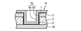
- the printed wiring board 1b of FIG. 5 includes a base material layer 2 mainly composed of a fluororesin, a first conductive layer 3 laminated on one surface of the base material layer 2, and the other of the base material layer 2.
- the base material layer 2 has the pre-processing surface 6 in which the content rate of an oxygen atom or a nitrogen atom is 0.2 atomic% or more on the inner peripheral surface of the base material layer 2 in the connection hole.
- the printed wiring board 1b has a modified layer 7 formed on the pretreated surface 6 on the inner peripheral surface of the base material layer 2 in the connection hole and having a hydrophilic organic functional group.
- the substrate layer 2, the first conductive layer 3, the pretreatment surface 6 and the modified layer 7 of the printed wiring board 1b of FIG. 5 are the substrate layer 2, the first conductive layer 3 and the front of the printed wiring board 1 of FIG. Since it is the same as that of the processing surface 6 and the modified layer 7, it attaches
- connection hole does not penetrate the second conductive layer 4b and exposes the inner side surface (the surface on the side laminated on the base material layer 2) of the second conductive layer 4b. Except for this point, the configuration of the second conductive layer 4b of the printed wiring board 1b of FIG. 5 is the same as the configuration of the second conductive layer 4 of the printed wiring board 1 of FIG. .
- the via hole 5b of the printed wiring board 1b in FIG. 5 includes the inner peripheral surface of the modified layer 7, the end surface in the connection hole of the first conductive layer 3, the region near the connection hole on the outer surface, and the connection hole of the second conductive layer 4b. It has the base conductor layer 8b laminated
- the method for manufacturing the printed wiring board 1b includes a step of preparing a laminate having the base material layer 2, the first conductive layer 3 and the second conductive layer 4b (a laminate preparation step), and forming a connection hole in the laminate.
- a step of forming a pretreatment surface 6 having a content of oxygen atoms or nitrogen atoms of 0.2 atomic% or more on the inner peripheral surface of the base material layer in the formed connection hole (previous step)
- a treatment surface forming step) a step of forming a modified layer 7 having a hydrophilic organic functional group on the inner peripheral surface of the connection hole in which the pretreated surface 6 is formed (modified layer forming step), and a modified layer 7
- connection hole forming process In the connection hole forming step, first, an opening is formed in the first conductive layer 3 as shown in FIG. 6A.
- the opening of the first conductive layer 3 can be formed, for example, by laminating a resist pattern on the first conductive layer 3 and performing etching.
- the material of the base layer 2 below the opening formed in the first conductive layer 3 is removed to form a connection hole.
- the material of the base material layer 2 can be removed by, for example, laser processing.
- the pretreatment surface 6 is formed at least on the end surface of the base material layer 2 (inner peripheral surface of the connection hole).
- the method for forming the pretreatment surface 6 is the same as the method for forming the pretreatment surface 6 in the pretreatment surface formation step of FIG.
- the modified layer forming step As shown in FIG. 6D, the end surface of the base material layer 2 is coated with a coupling agent having a hydrophilic organic functional group and capable of binding to the fluororesin. A reforming layer 7 in contact therewith is formed.
- the overlapping description is abbreviate
- ⁇ Via hole formation process> a step of laminating the underlying conductor layer 8b so as to be in contact with the inner peripheral surface of the modified layer 7 (underlying conductor layer laminating step) and a main conductor layer 9b are formed so as to be in contact with the surface of the underlying conductor layer 8b.
- a process main conductor layer forming process).
- the inner peripheral surface of the modified layer 7, the end surface in the connection hole of the first conductive layer 3, the region near the connection hole on the outer surface, and the second conductive layer 4b A base conductor layer 8b is formed on the inner surface of the connection hole by electroless plating.
- the electroless plating for forming the base conductor layer 8b can be the same as the electroless plating for forming the base conductor layer 8 in FIG. 2E.
- the via hole 5b of the printed wiring board 1b shown in FIG. 5 is formed by forming the main conductor layer 9b by laminating metals by electroplating using the base conductor layer 8b as the adherend. .
- the electroplating in this main conductor layer forming step can be the same as the electroplating for forming the main conductor layer 9 of the printed wiring board 1 of FIG.
- the conductive pattern is formed by etching the first conductive layer 3 and the second conductive layer 4b by a known etching method for forming a resist pattern by photolithography, for example.
- the printed wiring board 1b is not laminated with the end portion of the via hole 5b on the outer surface of the second conductive layer 4b, it can be easily laminated with other printed wiring boards, and is suitable for forming a multilayer substrate.
- the printed wiring board 1c of FIG. 7 includes a base material layer 2 mainly composed of a fluororesin, a first conductive layer 3 laminated on one surface of the base material layer 2, and the other of the base material layer 2.
- the second conductive layer 4b stacked on the surface is formed along a connection hole penetrating the base material layer 2 and the first conductive layer 3, and electrically connects the first conductive layer 3 and the second conductive layer 4b. And a via hole 5c.
- the said base material layer 2 has the pre-processing surface 6 whose content rate of an oxygen atom or a nitrogen atom is 0.2 atomic% or more in the internal peripheral surface of the base material layer 2 in the said connection hole.
- the printed wiring board 1c has a modified layer 7 formed on the pretreatment surface 6, that is, the inner peripheral surface of the connection hole, and having a hydrophilic organic functional group.
- the substrate layer 2, the first conductive layer 3, the second conductive layer 4b, the pretreatment surface 6 and the modified layer 7 of the printed wiring board 1c of FIG. 7 are the same as the substrate layer 2 of the printed wiring board 1b of FIG. Since it is the same as the 1 conductive layer 3, the 2nd conductive layer 4b, the pretreatment surface 6, and the modified layer 7, the same code
- the via hole 5c of the printed wiring board 1c in FIG. 7 includes a base conductor layer 8c laminated so as to be in contact with the inner peripheral surface of the modified layer 7, the inner peripheral surface of the base conductor layer 8c, and the connection hole of the first conductive layer 3. And the main conductor layer 9c laminated so as to be in contact with the inner surface in the connection hole of the second conductive layer 4b.
- the base conductor layer 8c of the printed wiring board 1c of FIG. 7 is a thin layer formed by solidifying conductive fine particles with a binder, and is used as an adherend when forming the main conductor layer 9c.
- the underlying conductor layer 8c is formed in a range connected to the first conductive layer 3 or the second conductive layer 4b.
- the material, thickness, and the like of the base conductor layer 8c can be the same as those of the base conductor layer 8a in the via hole 5a of the printed wiring board 1a shown in FIG.
- the main conductor layer 9c of the printed wiring board 1c of FIG. 7 includes the inner peripheral surface of the base conductor layer 8c, the end surface in the connection hole of the first conductive layer 3, the region near the connection hole on the outer surface, and the second conductive layer 4b. It is formed of a metal laminated by electroplating on the inner surface in the connection hole.
- the metal forming the main conductor layer 9c and the thickness of the main conductor layer 9c are the same as those of the main conductor layer 9 of the printed wiring board 1 in FIG.
- the method for manufacturing the printed wiring board 1c includes a step of preparing a laminate having the base material layer 2, the first conductive layer 3, and the second conductive layer 4b (laminate preparation step), and forming connection holes in the laminate.
- a step of forming a pretreatment surface 6 having a content of oxygen atoms or nitrogen atoms of 0.2 atomic% or more on the inner peripheral surface of the base material layer in the formed connection hole (previous step) A treatment surface forming step), a step of forming a modified layer 7 having a hydrophilic organic functional group on the inner peripheral surface of the connection hole in which the pretreated surface 6 is formed (modified layer forming step), and a modified layer 7 A step of forming the via hole 5c by laminating the base conductor layer 8c and the main conductor layer 9c so as to contact the inner peripheral surface of the formed connection hole (via hole forming step).
- the laminate preparation step, connection hole formation step, pretreatment surface formation step, and modified layer formation step in the method for manufacturing the printed wiring board 1c are the same as the laminate preparation step, connection in the method for manufacturing the printed wiring board 1b in FIG. Since it is the same as the hole forming step, the pretreatment surface forming step, and the modified layer forming step, a duplicate description is omitted.
- the via hole forming step includes a step of laminating the underlying conductor layer 8c so as to be in contact with the inner peripheral surface of the modified layer 7 (underlying conductor layer laminating step), and the connection of the inner peripheral surface of the underlying conductor layer 8c and the first conductive layer 3
- the surface potential of the inner peripheral surface of the connection hole formed in the laminate of the base material layer 2, the first conductive layer 3 and the second conductive layer 4b is adjusted by a conditioner to be colloidal.
- the conductive fine particles are adsorbed on the inner peripheral surface of the connection hole.
- the end surface of the first conductive layer 3 (inner peripheral surface of the connection hole) and the inner side surface of the second conductive layer 4b are exposed.
- the surface layer of the first conductive layer 3 and the second conductive layer 4b is removed by etching, so that the portion of the underlying conductor layer 8c attached to the surface of the first conductive layer 3 and the second conductive layer 4 is removed. To peel off.
- the main conductor layer 9c is formed by laminating a metal by electroplating with the base conductor layer 8c, the first conductive layer 3 and the second conductive layer 4b in the vicinity of the base conductor layer 8c as the adherend.
- the via hole 5c of the printed wiring board 1c shown in FIG. 7 is formed.
- the conductive pattern is formed by etching the first conductive layer 3 and the second conductive layer 4b by a known etching method for forming a resist pattern by photolithography, for example.
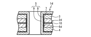
- a printed wiring board 1d of FIG. 8 includes a base material layer 2d having a reinforcing material 10 as a main component, a first conductive layer 3 laminated on one surface of the base material layer 2d, and the base material.
- the base material layer 2d has a pretreatment surface 6d having a content rate of oxygen atoms or nitrogen atoms of 0.2 atomic% or more on the inner peripheral surface of the base material layer 2d in the connection hole. Furthermore, the printed wiring board 1 further includes a modified layer 7 formed on the pretreatment surface 6d of the inner peripheral surface of the connection hole and having a hydrophilic organic functional group.
- the first conductive layer 3, the second conductive layer 4, the via hole 5 and the modified layer 7 of the printed wiring board 1d of FIG. 8 are the first conductive layer 3, the second conductive layer 4 and the via hole of the printed wiring board 1 of FIG. 5 and the modified layer 7, the same reference numerals are given and redundant description is omitted.
- the base material layer 2d of the printed wiring board 1d in FIG. 8 is formed from a resin composition containing a fluororesin as a main component, and the reinforcing material 10 is disposed inside.
- the base material layer 2d has the same configuration as the base material layer 2 of the printed wiring board 1 of FIG. 1 except that the reinforcing material 10 is provided. For this reason, the overlapping description is omitted.
- the reinforcing material 10 may be entirely dispersed inside the base material layer 2d, but is preferably arranged so as not to be exposed on the joint surface with the first conductive layer 3 or the second conductive layer 4, for example,
- the base material layer 2d is disposed in the center in the thickness direction.
- the reinforcing material 10 is not particularly limited as long as the coefficient of linear expansion is smaller than that of the base material layer 2d.
- the insulating material and the heat resistance that does not melt and flow at the melting point of the fluororesin are equivalent to the fluororesin. It is desirable to have the above tensile strength and corrosion resistance.
- the reinforcing material 10 include fibrous materials such as carbon fiber, glass fiber, aramid fiber, and alumina fiber. Moreover, as the reinforcing material 10 other than the fibrous material, a film-like material can also be used.
- the reinforcing material 10 made of a fibrous material may be disposed in the base material layer 2d in a state in which, for example, a fabric is formed, and in a state in which a filamentous body such as a separated state or a twisted yarn is formed, You may arrange
- the fibrous material fabric used as the reinforcing material 10 examples include a glass cloth in which glass is formed in a cloth shape, a fluororesin-containing glass cloth in which such a glass cloth is impregnated with a fluororesin, metal, ceramics, alumina, poly Examples thereof include resin cloth in which heat-resistant fibers such as tetrafluoroethylene (PTFE), polyether ether ketone (PEEK), polyimide (PI), and aramid are formed in a cloth shape or a nonwoven fabric.
- PTFE tetrafluoroethylene
- PEEK polyether ether ketone
- PI polyimide
- aramid a plain weave is preferable for thinning the base material layer 2d
- a twill weave or a satin weave is preferable for making the base material layer 2d bendable.
- a known weaving method can be applied.
- the film-like material used as the reinforcing material 10 examples include polytetrafluoroethylene (PTFE), liquid crystal polymer (LCP (type I)), polyimide, polyamideimide (PAI), polybenzimidazole (PBI), poly Examples thereof include heat-resistant films mainly composed of ether ether ketone, polytetrafluoroethylene, tetrafluoroethylene / perfluoroalkyl vinyl ether copolymer (PFA), thermosetting resin, cross-linked resin, and the like. Moreover, you may include the said fibrous material in these film-form materials.
- the pretreatment surface 6d is formed by surface treatment on the surface of the base material layer 2d (inner peripheral surface of the connection hole), and contains oxygen atoms or nitrogen atoms in the resin composition forming the base material layer 2d.
- the composition may be the same as the reinforcement material 10 inside the base material layer 2d, and the oxygen atom or the nitrogen atom may be increased.
- the pretreatment surface 6d of the printed wiring board 1d of FIG. 8 includes the oxygen atom or nitrogen atom content, the contact angle with respect to pure water, and the wetting tension in the portion excluding the reinforcing material 10; This is the same as the oxygen atom or nitrogen atom content of 6, the contact angle with pure water, and the wetting tension.
- the printed wiring board 1d is excellent in strength because the base material layer 2d has the reinforcing material 10.
- the reinforcing material 10 when the connection hole is formed in the base material layer 2d by, for example, drilling, the reinforcing material 10 generates cutting powder, and this cutting powder is the inner peripheral surface of the connection hole of the base material layer 2d.
- the surface is roughened by scratching. For this reason, the surface area of the connection hole of the base material layer 2d increases, and the formation of the pretreatment surface 6d is promoted. That is, the roughening of the connection hole by the reinforcing material 10 contributes to the increase in the content of oxygen atoms or nitrogen atoms, the contact angle with pure water, and the wetting tension of the pretreated surface 6d.
- the electrical connection between 3 and the second conductive layer 4 is made more reliable.
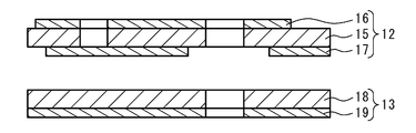
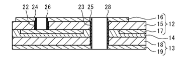
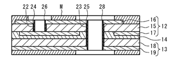
- the printed wiring board 11 of FIG. 9 includes a first substrate 12 and a second substrate 13 stacked on the other surface side of the first substrate 12.
- the first substrate 12 and the second substrate 13 are laminated via an adhesive 14.
- the first substrate 12 includes a first base material layer 15 mainly composed of a fluororesin, a first conductive layer 16 laminated on one surface of the first base material layer 15, and the first base material layer 15. And the second conductive layer 17 stacked on the other surface.
- the second substrate 13 includes a second base material layer 18 mainly composed of a fluororesin, and a third conductive layer 19 laminated on the other surface of the second base material layer 18.
- the adhesive agent 14 Although it does not specifically limit as the adhesive agent 14, The thing excellent in the softness
- the resin as the main component of the adhesive 14 include epoxy resin, polyimide, unsaturated polyester, saturated polyester, butadiene resin, acrylic resin, polyamide, polyolefin, silicone, fluorine resin, urethane resin, styrene resin, and butyral resin. , Modified polyphenylene ether, polyetheretherketone, polyamideimide, polyethersulfone, syndiotactic polystyrene, or a resin containing one or more of these. Moreover, you may use as a material of adhesive agent resin obtained by bridge
- thermosetting resin As a main component of the adhesive 14, a thermosetting resin is preferable.
- the lower limit of the curing temperature of the thermosetting resin that is the main component of the adhesive 14 is preferably 120 ° C., more preferably 150 ° C.
- the upper limit of the curing temperature of the thermosetting resin that is the main component of the adhesive 14 is preferably 230 ° C, more preferably 200 ° C.
- the curing temperature of the thermosetting resin that is the main component of the adhesive 14 is less than the lower limit, it may be difficult to handle the adhesive that is the raw material of the adhesive 14.
- the curing temperature of the thermosetting resin that is the main component of the adhesive 14 exceeds the above upper limit, the first base material layer 15 and the second base layer 15 are formed when the adhesive is cured to form the adhesive 14. If the base material layer 18 is deformed by heat, the dimensional accuracy of the printed wiring board may be impaired.
- the printed wiring board 11 is formed along a connection hole penetrating the first conductive layer 16 and the first base material layer 15 in the thickness direction, and the first conductive layer 16 and the second conductive layer 17 are electrically connected.
- a second via hole 21 formed and electrically connecting the first conductive layer 16 and the third conductive layer 19.
- the printed wiring board 11 has a first pretreated surface having a content ratio of oxygen atoms or nitrogen atoms of 0.2 atomic% or more on the inner peripheral surface of the connection hole of the first via hole 20 of the first base material layer 15. 22. Further, the content rate of oxygen atoms or nitrogen atoms is 0.2 atomic% or more on the inner peripheral surface of the connection hole of the second via hole 21 of the first base material layer 15, the adhesive 14, and the second base material layer 18. A second pretreatment surface 23 is formed.
- the printed wiring board 11 is formed in the formation region of the first pretreatment surface 22 and is formed in the formation region of the first modified layer 24 having the hydrophilic organic functional group and the second pretreatment surface 23.
- a second modified layer 25 formed and having a hydrophilic organic functional group.
- the first base material layer 15 and the second base material layer 18 of the printed wiring board 11 of FIG. 9 are the same as the base material layer 2 of the printed wiring board 1 of FIG. Moreover, the 1st conductive layer 16, the 2nd conductive layer 17, and the 3rd conductive layer 19 of the printed wiring board 11 of FIG. 9 are the same as the 1st conductive layer 3 and the 2nd conductive layer 4 of the printed wiring board 1 of FIG. It is said. Furthermore, the first pretreatment surface 22 and the first and modified layer 24 of the printed wiring board 11 of FIG. 9 are the same as the pretreatment surface 6 and the modified layer 7 of the printed wiring board 1 of FIG. The second pretreatment surface 23 and the second modified layer 25 of the printed wiring board 11 of FIG.
- the first via hole 20 includes a first base conductor layer 26 laminated so as to be in contact with the inner peripheral surface of the first modified layer 24 and the end surface in the connection hole of the first conductive layer 16 (inner peripheral surface of the connection hole). Of the inner peripheral surface of the first base conductor layer 26, one surface of the second conductive layer 17 exposed in the connection hole, and one of the surfaces of the first conductive layer 16 adjacent to the connection hole And a first main conductor layer 27 stacked over the two.
- the configuration of the first base conductor layer 26 and the first main conductor layer 27 of the printed wiring board 11 of FIG. 9 is the same as that of the base conductor layer 8 and the main conductor layer 9 of the printed wiring board 1 of FIG. And can be similar. Therefore, a duplicate description of these configurations is omitted.
- the via hole 21 includes an inner peripheral surface of the second modified layer 25, an end surface in the connection hole of the first conductive layer 16 (an inner peripheral surface of the connection hole), and an end surface in the connection hole of the third conductive layer 19.
- the second main conductor layer 29 stacked over the region adjacent to the connection hole in the other surface.
- the configurations of the second base conductor layer 28 and the first second main conductor layer 29 of the printed wiring board 11 of FIG. 9 are the same as those of the base conductor layer 8 and the main conductor of the printed wiring board 1 of FIG. It can be similar to layer 9. For this reason, the overlapping description about these structures is abbreviate
- the method for manufacturing the printed wiring board 11 includes a step of preparing the first substrate 12 and the second substrate 13 (substrate preparation step), and a step of forming connection holes in the first substrate 12 and the second substrate 13 (connection hole formation). Step), a step of laminating the first substrate 12 and the second substrate 13 with the adhesive 14 (substrate laminating step), and a step of forming the first pretreatment surface 22 and the second pretreatment surface 23 (pretreatment surface formation).
- Step 1) a step of forming a first modified layer and a second modified layer having a hydrophilic organic functional group so as to be in contact with the inner peripheral surface of the connection hole (modified layer forming step), A step of laminating the first base conductor layer 26 and the second base conductor layer 28 so as to be in contact with the peripheral surface (base conductor layer stacking step), a surface on one side of the first substrate 12, and a surface on the other side of the second substrate 13; Forming a plating mask M in which a region adjacent to the connection hole is opened (mass Forming step) and the first main conductor layer on the first base conductor layer 26, the second base conductor layer 28, the first conductive layer 16, the second conductive layer 17 and the third conductive layer 19 in the opening of the plating mask M. 27 or the second main conductor layer 29 is selectively laminated (main conductor layer lamination step), and the plating mask M is removed (mask removal step).
- the substrate preparation step the first substrate 12 patterned with the first conductive layer 16 and the second conductive layer 17 and the second substrate 13 patterned with the third conductive layer 19 are prepared. Since the first substrate 12 and the second substrate 13 are publicly known, the description of the formation method is omitted.
- connection hole forming process connection holes are formed in the first substrate 12 and the second substrate 13 as shown in FIG. 10A.
- the method for forming the connection hole can be the same as the method for forming the connection hole in FIG. 2B.
- the first substrate 12 and the second substrate 13 are stacked with an adhesive 14 as shown in FIG. 10B.
- the adhesive 14 is laminated so as not to block the connection hole of the second substrate 13.
- the adhesive 14 is laminated on the other surface of the first substrate 12 or the one surface of the second substrate 13, and the first substrate 12 or the adhesive 14 is laminated.
- a connection hole that penetrates the layer of the adhesive 14 may be formed in the second substrate.
- the first pretreatment surface 22 is formed on the inner peripheral surface of the connection hole of the first base material layer 15, and the first base material layer 15, the adhesive 14, and A second pretreatment surface 23 is formed on the inner peripheral surface of the connection hole of the second base material layer 18.
- the formation method of the first pretreatment surface 22 and the second pretreatment surface 23 can be the same as the formation method of the pretreatment surface 6 in FIG. 2C.
- the first modified layer 24 and the second modified layer 25 are formed so as to be in contact with the first pretreated surface 22 and the second pretreated surface 23.
- the method for forming the first modified layer 24 and the second modified layer 25 can be the same as the method for forming the modified layer 7 in FIG. 2D.
- ⁇ Mask formation process> In the mask formation step, as shown in FIG. 10F, a region adjacent to the connection hole is opened on one surface of the first substrate 12 and the other surface of the second substrate 13, and the first conductive layer 16 and the third conductive layer 16 are formed. A plating mask M that partially exposes the conductive layer 19 is formed.
- the plating mask M for example, a known resist film that can be patterned by a photolithography technique can be used. Since a method for forming the plating mask M using such a photolithography technique is known, a detailed description thereof will be omitted.
- the first conductive layer 16 and the second conductive layer 28 exposed from the plating mask M and the first conductive layer 16 and the third conductive layer 19 are used as adherends, and metal is deposited by electroplating.
- metal is deposited by electroplating.
- the electroplating in this main conductor layer laminating step can be the same as the electroplating for laminating the main conductor layer 9 of the printed wiring board 1 of FIG.
- the printed wiring board 11 is brought into the state shown in FIG. 9 by removing the plating mask M.
- the method for removing the plating mask M include a method using a stripping solution that is appropriately selected according to the material of the plating mask M.
- a stripping solution that can be used for removing the plating mask M a commercially available one can be used, and a detailed description thereof will be omitted.
- the modified wiring layer can be omitted in the printed wiring board of the present invention.
- the modified layer forming step can be omitted.
- the printed wiring board of the present invention does not require that the pretreatment surface be formed on the entire inner peripheral surface of the base material layer in the connection hole. That is, the pretreatment surface may be partially formed on a part of the inner peripheral surface of the base material layer in the connection hole.
- the via hole may have a single layer structure formed of silver paste, solder paste, or the like without forming the underlying conductor layer.
- the first, second, and third numbers given to the names of the constituent elements of the printed wiring board of the present invention are given for convenience in order to distinguish the constituent elements. Therefore, the numbers given to the components in each embodiment can be read as appropriate.
- a conductive layer in which a main conductor layer is laminated after forming a via hole as in the first to fifth embodiments, regardless of the configuration of the printed wiring board to be manufactured.
- a circuit pattern may be formed by patterning, and a via hole connecting conductive layers may be formed by selectively laminating a main conductive layer on a patterned conductive layer as in the sixth embodiment. Good.
- the same laminated structure as the via hole of the printed wiring board of the present invention was prototyped and the effect of forming the pretreatment surface and the modified layer was evaluated.
- a sample is obtained in which a surface of a base film mainly composed of tetrafluoroethylene / hexafluoropropylene copolymer (FEP) is surface-treated with a plurality of plasma gases to form different pretreated surfaces. It was. Further, a sample in which a modified layer was laminated by applying (modifying treatment) a coupling agent on the surface of the base film on which the pretreated surface was formed and the surface of the base film not subjected to the surface treatment was obtained.
- FEP tetrafluoroethylene / hexafluoropropylene copolymer
- samples in which an underlying conductor layer was formed on the surfaces of these samples by electroless copper plating were obtained.
- a base conductor layer is formed by electroless copper plating on the pretreated surface without modifying the base film on which the pretreated surface is formed, and the surface of the base conductor layer is further thickened by electrolytic copper plating.
- a sample in which a main conductor layer of 15 ⁇ m was formed was obtained.
- the base film used what does not contain an oxygen atom or a nitrogen atom substantially.
- the plasma gas oxygen, water vapor, argon, ammonia or nitrogen was used. Further, 3-aminopropyltrimethoxysilane (silane coupling agent) was used as a coupling agent for forming the modified layer.
- silane coupling agent silane coupling agent
- Table 1 shows the oxygen content and nitrogen content of the pretreated surface, the evaluation result of the pure water contact angle reduction effect in the surface treatment, the evaluation result of the surface resistance reduction effect in the surface treatment, and the modified layer The evaluation result of the surface resistance reduction effect by formation and the evaluation result of peeling strength are shown.
- Oxygen content and “nitrogen content” are values measured by X-ray photoelectron spectroscopy, assuming that the X-ray source is an aluminum metal K alpha ray, the beam diameter is 50 ⁇ m, and the X-ray incident angle to the analysis surface is 45 °. It is. Note that “ ⁇ 0.05%” in the table means that the content rate was lower than 0.05%, which is the detection limit of the measuring device, and measurement was not possible.
- the effect of reducing the contact angle with pure water in the surface treatment means that the reduction rate of the contact angle with pure water on the pretreated surface relative to the contact angle with pure water on the surface of the untreated base film is less than 1%.
- the reduction rate is 1% or more and less than 10%, “C”, the reduction rate is 10% or more and less than 20%, “B”, and the reduction rate is 20% or more, “A”.
- the pure water surface contact angle when not treated was 100 °.
- the “surface resistance reduction effect in surface treatment” means that the reduction ratio of the surface resistance of the base conductor layer formed on the pretreated surface relative to the base conductor layer formed on the untreated base film surface is less than 1% “D”
- the reduction rate was 1% or more and less than 10%, “C”, the reduction rate was 10% or more and less than 20%, “B”, and the reduction rate was 20% or more, “A”.
- the resistance value was measured as a resistance value between two points 10 mm away from the electroless copper plating surface.
- “Surface resistance reduction effect by modification treatment” means “B” when the reduction ratio of the surface resistance of the underlying conductor layer formed on the modified layer relative to the underlying conductor layer formed on the pretreated surface is less than 10%. A rate of 10% or more was defined as “A”.
- “Peel strength of the conductive layer” refers to the sample in which the main conductor layer is formed in accordance with JIS-K-6854-2 (1999) “Adhesive—Peeling adhesive strength test method—Part 2: 180 degree peeling”. A glass epoxy resin reinforcing plate is adhered to the back surface of the base film with an adhesive, and the laminate of the base conductor layer and the main conductor layer is measured as a flexible adherend, and less than 0.1 N / cm is “D”. 0.1 N / cm or more and less than 1.0 N / cm was designated as “C”, 1.0 N / cm or more and less than 3.0 N / cm as “B”, and 3.0 N / cm or more as “A”. In Table 1, “-” means that the sample was not measured.
- the contact resistance with pure water is sufficiently reduced by forming a pretreated surface having an oxygen atom or nitrogen atom content of 0.2 atomic% or more, and the surface resistance of the conductive layer formed thereon It was confirmed that the thickness of the conductive layer can be sufficiently reduced and the peel strength of the conductive layer can be improved.
- the surface resistance reduction effect in the modification treatment was good regardless of the type and degree of the surface treatment.
- the surface resistance reduction rate was less than 10% when only the modification treatment was performed without performing the surface treatment.
- the effect of improving the adhesion is improved by combining the reforming treatment with the pretreatment surface.
- the printed wiring board according to the present invention is particularly preferably used as a highly integrated wiring board that transmits high-frequency signals.
Landscapes
- Engineering & Computer Science (AREA)
- Microelectronics & Electronic Packaging (AREA)
- Manufacturing & Machinery (AREA)
- Printing Elements For Providing Electric Connections Between Printed Circuits (AREA)
- Manufacturing Of Printed Wiring (AREA)
- Laminated Bodies (AREA)
Abstract
本発明は、フッ素樹脂を主成分とする基材層の両面に形成された導電層がビアホールによって確実に接続されるプリント配線板を提供することを課題とする。本発明の一態様に係るプリント配線板は、フッ素樹脂を主成分とする基材層と、この基材層の一方の面に積層される第1導電層と、上記基材層の他方の面に積層される第2導電層と、上記基材層と上記第1導電層及び第2導電層の少なくとも一方とを厚さ方向に貫通する接続孔に沿って形成され、上記第1導電層及び第2導電層を電気的に接続するビアホールとを備えるプリント配線板であって、上記接続孔における上記基材層の内周面の少なくとも一部に、酸素原子又は窒素原子の含有率が0.2atomic%以上の前処理表面を有する。
Description
本発明は、プリント配線板及びプリント配線板の製造方法に関する。
電気信号を伝送するプリント配線板では、伝送する電気信号の周波数が高くなると、導体周囲の絶縁材料による誘電損が大きくなる。このため、プリント配線板において、導電層を形成するための基材の主成分を誘電率及び誘電正接が小さいフッ素樹脂とすることが提案されている(特開2013-165171号公報参照)。
また、電子機器の小型化に伴ってプリント配線板の配線密度を高めることが望まれるため、複数の導電層を形成した多層プリント配線板が利用される。そのような多層プリント配線板では、異なる導電層間を接続するビアホール(筒状の導体)が形成される。このようなビアホールの形成方法としては、プリント配線板に穴を開け、この穴の内周面に無電解めっきを施してから電気めっきにより2つ以上の導電層間を接続する金属層を形成する方法が知られている。また、プリント配線板の穴の内周面に導電性微粒子の層を形成してから無電解めっき及び電気めっきを行う技術も提案されている(特開2013-214785号公報参照)。
フッ素樹脂を主成分とする基材層の両面に導電層を形成し、これらの導電層をビアホールによって接続する場合、フッ素樹脂表面の接着性が低いため、ビアホールの形成が容易ではない。例えばフッ素樹脂を主成分とする基材層を用いたプリント配線板の製造に上記特開2013-214785号公報に記載されたビアホールの形成方法を適用する場合、フッ素樹脂を主成分とする基材が導電性微粒子を含むインク等をはじくため、導電性微粒子の層を上手く形成できないおそれがある。
本発明は、上記不都合に鑑みてなされたものであり、フッ素樹脂を主成分とする基材層の両面に形成された導電層がビアホールによって確実に接続されるプリント配線板及びそのようなプリント配線板の製造方法を提供することを課題とする。
上記課題を解決するためになされた本発明の一態様に係るプリント配線板は、フッ素樹脂を主成分とする基材層と、この基材層の一方の面に積層される第1導電層と、上記基材層の他方の面に積層される第2導電層と、上記基材層と上記第1導電層及び第2導電層の少なくとも一方とを厚さ方向に貫通する接続孔に沿って形成され、上記第1導電層及び第2導電層を電気的に接続するビアホールとを備えるプリント配線板であって、上記接続孔における上記基材層の内周面の少なくとも一部に、酸素原子又は窒素原子の含有率が0.2atomic%以上の前処理表面を有する。
また、上記課題を解決するためになされた別の態様に係るプリント配線板の製造方法は、フッ素樹脂を主成分とする基材層と、この基材層の一方の面に積層される第1導電層と、上記基材層の他方の面に積層される第2導電層と、上記第1導電層及び第2導電層を電気的に接続するビアホールとを備えるプリント配線板の製造方法であって、上記基材層と上記第1導電層及び第2導電層の少なくとも一方とを貫通する接続孔を形成する工程と、上記接続孔における上記基材層の内周面の少なくとも一部に、酸素原子又は窒素原子の含有率が0.2atomic%以上の前処理表面を形成する工程と、上記接続孔の内周面に下地導体層及び主導体層を積層して上記ビアホールを形成する工程とを備える。
本発明のプリント配線板は、フッ素樹脂を主成分とする基材層の両面に形成された導電層がビアホールによって確実に接続される。また、本発明のプリント配線板の製造方法は、フッ素樹脂を主成分とする基材層の両面に形成された導電層をビアホールによって確実に接続できる。
[本発明の実施形態の説明]
本発明の一態様に係るプリント配線板は、フッ素樹脂を主成分とする基材層と、この基材層の一方の面に積層される第1導電層と、上記基材層の他方の面に積層される第2導電層と、上記基材層と上記第1導電層及び第2導電層の少なくとも一方とを厚さ方向に貫通する接続孔に沿って形成され、上記第1導電層及び第2導電層を電気的に接続するビアホールとを備えるプリント配線板であって、上記接続孔における上記基材層の内周面の少なくとも一部に、酸素原子又は窒素原子の含有率が0.2atomic%以上の前処理表面を有する。
本発明の一態様に係るプリント配線板は、フッ素樹脂を主成分とする基材層と、この基材層の一方の面に積層される第1導電層と、上記基材層の他方の面に積層される第2導電層と、上記基材層と上記第1導電層及び第2導電層の少なくとも一方とを厚さ方向に貫通する接続孔に沿って形成され、上記第1導電層及び第2導電層を電気的に接続するビアホールとを備えるプリント配線板であって、上記接続孔における上記基材層の内周面の少なくとも一部に、酸素原子又は窒素原子の含有率が0.2atomic%以上の前処理表面を有する。
当該プリント配線板は、接続孔における基材層の内周面の少なくとも一部に、酸素原子又は窒素原子の含有率が0.2atomic%以上のフッ素樹脂の接着性の低さを補う前処理表面を有するので、この前処理表面がビアホールに対する高い密着性を発揮する。これにより、当該プリント配線板は、基材層の両側の第1導電層及び第2導電層をビアホールによって確実に接続することができ、かつ前処理表面によってビアホールの剥離が防止されるので信頼性が高い。また、当該プリント配線板は、前処理表面を有することによってビアホールの積層が容易であるため、製造が容易で安価に提供できる。
上記接続孔における基材層の内周面のうち少なくとも上記前処理表面の形成領域に、親水性有機官能基を有する改質層をさらに備えるとよい。このように上記接続孔における基材層の内周面のうち少なくとも上記前処理表面の形成領域に、親水性有機官能基を有する改質層を備えることで、基材層とビアホールとの密着性がさらに大きくなり、製造効率及び信頼性をより向上できる。
上記ビアホールが、上記接続孔の内周面に接する下地導体層と、この下地導体層の内周面に接する主導体層とを有するとよい。このように下地導体層の上に主導体層を設けることにより、第1導電層及び第2導電層間を接続するビアホールを容易かつ確実に形成できる。
上記前処理表面の純水との接触角としては90°以下が好ましい。このように前処理表面の純水との接触角を上記上限以下とすることによって、ビアホールの積層が容易となり、第1導電層及び第2導電層間の接続がより確実になる。
上記ビアホールと基材層との間の剥離強度としては、1.0N/cm以上が好ましい。このように上記ビアホールと基材層との間の剥離強度を上記下限以上とすることによって、接続孔における基材層の内周面からのビアホールの剥離及びこれに起因するビアホールの第1導電層又は第2導電層からの剥離が防止される。これにより、第1導電層及び第2導電層間の接続がより確実になる。
また、本発明の別の態様に係るプリント配線板の製造方法は、フッ素樹脂を主成分とする基材層と、この基材層の一方の面に積層される第1導電層と、上記基材層の他方の面に積層される第2導電層と、上記第1導電層及び第2導電層を電気的に接続するビアホールとを備えるプリント配線板の製造方法であって、上記基材層と上記第1導電層及び第2導電層の少なくとも一方とを貫通する接続孔を形成する工程と、上記接続孔における上記基材層の内周面の少なくとも一部に、酸素原子又は窒素原子の含有率が0.2atomic%以上の前処理表面を形成する工程と、上記接続孔の内周面に下地導体層及び主導体層を積層して上記ビアホールを形成する工程とを備える。
当該プリント配線板の製造方法は、接続孔における基材層の内周面の少なくとも一部に、酸素原子又は窒素原子の含有率が0.2atomic%以上の前処理表面を形成することよって、基材層とビアホールとの接着性を向上させるので、下地導体層及び主導体層を積層してビアホールを形成するのが容易であり、第1導電層及び第2導電層間を容易かつ確実に接続できる。このため、当該プリント配線板の製造方法は、安価で信頼性の高いプリント配線板の提供を可能にする。
上記下地導体層が導電性材料の付着又は銅の無電解めっきにより形成されるとよい。このように、下地導体層を導電性材料の付着又は銅の無電解めっきにより形成することによって、下地導体層の積層が簡単であり、さらに主導体層の積層を確実なものとすることができる。
ここで、「酸素原子又は窒素原子の含有率」は、例えばX線光電子分光法(ESCA:Electron Spectroscopy for Chemical Analysis又はXPS:X-ray Photoelectron Spectroscopy)、エネルギー分散型X線分光法(EDX:Energy Dispersive X-ray Spectroscopy又はEDS:Energy Dispersive X-ray Spectroscopy)、電子プローブマイクロアナリシス法(EPMA:Electron Probe Micro Analysis)、飛行時間型二次イオン質量分析法(TOF-SIMS:Time Of Flight Secondary Ion Mass Spectrometry)、二次イオン質量分析法(SIMS:Secondary Ion Mass Spectrometry)、オージェ電子分光法(AES:Auger Electron Spectroscopy)、電子顕微鏡等により測定することができる。X線光電子分光法による場合は、測定条件として、X線源をアルミニウム金属のKアルファ線、ビーム径を50μm、分析表面に対するX線入射角度を45°とし、表面を走査することによって測定することができる。装置としては、例えばULVAC-Phi社の「Quantera」を使うことができる。上記測定時の測定表面(前処理表面等)は、測定表面を覆っている導体層(金属等)を例えばエッチング等によって除去することによって露出させることができる。なお、測定表面が表出していない場合、スパッタリングにより材料を測定表面と垂直な方向に順に除去することによって、任意の深さ位置における原子の組成割合を上記方法によって測定することができる。また、測定表面の断面であっても、測定表面とほぼ平行な方向にスパッタリングで除去しながらSIMSなどで深さ方向の不純物濃度を分析しつつ、電子顕微鏡で表面処理層の厚みを測定するなど、上記方法を種々組み合わせて評価することによって表面の酸素原子又は窒素原子の含有率を測定することができる。また、「純水との接触角」とは、JIS-R-3257(1999)の静滴法により測定される接触角の値である。また「剥離強度」とは、JIS-K-6854-2(1999)「接着剤-はく離接着強さ試験方法-2部:180度はく離」に準拠し測定される値である。
[本発明の実施形態の詳細]
以下、本発明に係るプリント配線板の各実施形態について図面を参照しつつ詳説する。
以下、本発明に係るプリント配線板の各実施形態について図面を参照しつつ詳説する。
〔第一実施形態〕
図1のプリント配線板1は、フッ素樹脂を主成分とする基材層2と、この基材層2の一方の面に積層される第1導電層3と、上記基材層2の他方の面に積層される第2導電層4と、上記基材層2、第1導電層3及び第2導電層4を厚さ方向に貫通する接続孔に沿って形成され、第1導電層3及び第2導電層4を電気的に接続するビアホール5とを主に備える。また、上記基材層2は、上記接続孔における基材層2の内周面に、酸素原子又は窒素原子の含有率が0.2atomic%以上の前処理表面6を有する。さらに、当該プリント配線板1は、上記基材層の内周面のうち少なくとも前処理表面6の形成領域に、かつ親水性有機官能基を有する改質層7をさらに備える。
図1のプリント配線板1は、フッ素樹脂を主成分とする基材層2と、この基材層2の一方の面に積層される第1導電層3と、上記基材層2の他方の面に積層される第2導電層4と、上記基材層2、第1導電層3及び第2導電層4を厚さ方向に貫通する接続孔に沿って形成され、第1導電層3及び第2導電層4を電気的に接続するビアホール5とを主に備える。また、上記基材層2は、上記接続孔における基材層2の内周面に、酸素原子又は窒素原子の含有率が0.2atomic%以上の前処理表面6を有する。さらに、当該プリント配線板1は、上記基材層の内周面のうち少なくとも前処理表面6の形成領域に、かつ親水性有機官能基を有する改質層7をさらに備える。
<基材層>
上記基材層2は、フッ素樹脂を主成分とする。ここで、フッ素樹脂とは、高分子鎖の繰り返し単位を構成する炭素原子に結合する水素原子の少なくとも1つが、フッ素原子又はフッ素原子を有する有機基(以下「フッ素原子含有基」ともいう)で置換されたものをいう。フッ素原子含有基は、直鎖状又は分岐状の有機基中の水素原子の少なくとも1つがフッ素原子で置換されたものであり、例えばフルオロアルキル基、フルオロアルコキシ基、フルオロポリエーテル基等を挙げることができる。
上記基材層2は、フッ素樹脂を主成分とする。ここで、フッ素樹脂とは、高分子鎖の繰り返し単位を構成する炭素原子に結合する水素原子の少なくとも1つが、フッ素原子又はフッ素原子を有する有機基(以下「フッ素原子含有基」ともいう)で置換されたものをいう。フッ素原子含有基は、直鎖状又は分岐状の有機基中の水素原子の少なくとも1つがフッ素原子で置換されたものであり、例えばフルオロアルキル基、フルオロアルコキシ基、フルオロポリエーテル基等を挙げることができる。
「フルオロアルキル基」とは、少なくとも1つの水素原子がフッ素原子で置換されたアルキル基を意味し、「パーフルオロアルキル基」を含む。具体的には、「フルオロアルキル基」は、アルキル基の全ての水素原子がフッ素原子で置換された基、アルキル基の末端の1個の水素原子以外の全ての水素原子がフッ素原子で置換された基等を含む。
「フルオロアルコキシ基」とは、少なくとも1つの水素原子がフッ素原子で置換されたアルコキシ基を意味し、「パーフルオロアルコキシ基」を含む。具体的には、「フルオロアルコキシ基」は、アルコキシ基の全ての水素原子がフッ素原子で置換された基、アルコキシ基の末端の1個の水素原子以外の全ての水素原子がフッ素原子で置換された基等を含む。
「フルオロポリエーテル基」とは、繰り返し単位としてオキシアルキレン単位を有し、末端にアルキル基又は水素原子を有する1価の基であって、このアルキレンオキシド鎖又は末端のアルキル基の少なくとも1つの水素原子がフッ素原子で置換された1価の基を意味する。「フルオロポリエーテル基」は、繰り返し単位として複数のパーフルオロアルキレンオキシド鎖を有する「パーフルオロポリエーテル基」を含む。
基材層2を構成するフッ素樹脂としては、例えばポリテトラフルオロエチレン(PTFE)、ポリテトラフルオロエチレン・パーフルオロアルキルビニルエーテル共重合体(PFA)、テトラフルオロエチレン・ヘキサフルオロプロピレン共重合体(FEP)、テトラフルオロエチレン・エチレン共重合体(ETFE)、ポリビニリデンフルオライド(PVDF)、ポリクロロトリフルオロエチレン(PCTFE)、クロロトリフルオロエチレン・エチレン共重合体(ECTFE)、ポリフッ化ビニル(PVF)、並びにテトラフルオロエチレン、ヘキサフルオロプロピレン、ビニリデンフルオライドの3種類のモノマーからなる熱可塑性フッ素樹脂(THV)及びフロオロエラストマーを挙げることができる。また、これらの化合物を含む混合物やコポリマーも、基材層2を構成する材料として使用可能である。
中でも、基材層2を構成するフッ素樹脂としては、テトラフルオロエチレン・ヘキサオロプロピレン共重合体(FEP)、ポリテトラフルオロエチレン・パーフルオロアルキルビニルエーテル共重合体(PFA)、又はポリテトラフルオロエチレン(PTFE)が好ましい。これらのフッ素樹脂を使用することによって、基材層2が、可撓性、光透過性、耐熱性及び難燃性を有するものとなる。
また、基材層2は、任意成分として、例えばエンジニアリングプラスチック、難燃剤、難燃助剤、顔料、酸化防止剤、反射付与剤、隠蔽剤、滑剤、加工安定剤、可塑剤、発泡剤等を含み得る。
上記エンジニアリングプラスチックとしては、基材層2に求められる特性に応じて例えばポリアセタール、ポリアミド、ポリカーボネート、変性ポリフェニレンエーテル、ポリブチレンテレフタレート、液晶ポリマー等、公知のものから選択して使用でき、典型的には芳香族ポリエーテルケトン樹脂を使用することができる。
この芳香族ポリエーテルケトンは、ベンゼン環がパラ位に結合し、剛直なケトン結合(-C(=O)-)又はフレキシブルなエーテル結合(-O-)によってベンゼン環同士が連結された構造を有する熱可塑性樹脂である。芳香族ポリエーテルケトンとしては、例えばエーテル結合、ベンゼン環、エーテル結合、ベンゼン環、ケトン結合及びベンゼン環が、この順序で並んだ構造単位を有するポリエーテルエーテルケトン(PEEK)、エーテル結合、ベンゼン環、ケトン結合及びベンゼン環が、この順序で並んだ構造単位を有するポリエーテルケトン(PEK)を挙げることができる。中でも、芳香族ポリエーテルケトンとしては、PEEKが好ましい。このような芳香族ポリエーテルケトンは、耐摩耗性、耐熱性、絶縁性、加工性等に優れる。
PEEK等の芳香族ポリエーテルケトンとしては、市販品を使用することができる。芳香族ポリエーテルケトンとしては、様々なグレードのものが市販されており、市販されている単一のグレードの芳香族ポリエーテルケトンを単独で使用してもよく、複数のグレードの芳香族ポリエーテルケトンを併用してもよく、また変性した芳香族ポリエーテルケトンを使用してもよい。
基材層2におけるエンジニアリングプラスチックの合計含有量の上記フッ素樹脂に対する比の下限としては、特に限定されないが、10質量%が好ましく、20質量%がより好ましく、35質量%がさらに好ましい。一方、エンジニアリングプラスチックの合計含有量の上記フッ素樹脂に対する比の上限としては、特に限定されないが、50質量%が好ましく、45質量%がより好ましい。エンジニアリングプラスチックの合計含有量が上記下限に満たない場合、基材層2の特性を十分に改善することができないおそれがある。また、エンジニアリングプラスチックの含有量が上記上限を超える場合、フッ素樹脂の有利な特性を十分に発現させることができないおそれがある。
難燃剤としては、公知の種々のものを使用することができ、例えば臭素系難燃剤、塩素系難燃剤等のハロゲン系難燃剤を挙げることができる。
難燃助剤としては、公知の種々のものを使用することができ、例えば三酸化アンチモン等を挙げることができる。
顔料としては、公知の種々のものを使用することができ、例えば酸化チタン等を挙げることができる。
酸化防止剤としては、公知の種々のものを使用することができ、例えばフェノール系酸化防止剤等を挙げることができる。
反射付与剤としては、公知の種々のものを使用することができ、例えば酸化チタン等を挙げることができる。
また、基材層2に中空構造を設けてもよい。
基材層2の平均厚さの下限としては、3μmが好ましく、6μmがより好ましい。一方、基材層2の平均厚さの上限としては、100μmが好ましく、55μmがより好ましい。基材層2の平均厚さが上記下限に満たない場合、当該プリント配線板1の強度が不十分となるおそれがある。また、基材層2の平均厚さが上記上限を超える場合、基材層2ひいては当該プリント配線板1の可撓性が不十分となるおそれがある。
(前処理表面)
前処理表面6は、基材層2の表面(接続孔の内周面)への表面処理によって形成され、酸素原子又は窒素原子を含有する。換言すると、この前処理表面6は、基材層2の内部とは異なる原子組成を有する表面である。この前処理表面6は、接続孔における基材層の内周面の全面に形成されている。
前処理表面6は、基材層2の表面(接続孔の内周面)への表面処理によって形成され、酸素原子又は窒素原子を含有する。換言すると、この前処理表面6は、基材層2の内部とは異なる原子組成を有する表面である。この前処理表面6は、接続孔における基材層の内周面の全面に形成されている。
前処理表面6の酸素原子又は窒素原子の含有率の下限としては、0.2atomic%であり、1atomic%が好ましく、5atomic%がより好ましい。一方、前処理表面6の酸素原子又は窒素原子の含有率の上限としては、30atomic%が好ましく、20atomic%がより好ましい。前処理表面6の酸素原子又は窒素原子の含有率が上記下限に満たない場合、前処理表面6のビアホール5に対する密着性が不十分となるおそれがある。また、前処理表面6の酸素原子又は窒素原子の含有率が上記上限を超える場合、フッ素樹脂の誘電率や誘電正接が大きくなるおそれがある。なお、前処理表面6のビアホール5に対する密着性とは、前処理表面6に直接ビアホール5が積層される場合だけでなく、前処理表面6に改質層7を介してビアホール5が積層される場合にも、ビアホール5の剥離し難さを意味するものとする。
前処理表面6の純水に対する接触角の上限としては、90°が好ましく、80°がより好ましい。一方、前処理表面6の純水に対する接触角の下限は特に限定されない。前処理表面6の純水に対する接触角が上記上限を超える場合、前処理表面6とビアホール5又は改質層7との接着強度が不十分となるおそれがある。なお、純水に対する接触角は、ERMA社の接触角測定器「G-I-1000」等を用いて測定できる。
前処理表面6の濡れ張力の下限としては、50mN/mが好ましく、60mN/mがより好ましい。前処理表面6の濡れ張力が上記下限に満たない場合、前処理表面6とビアホール5との密着力が不足し、ビアホール5が剥離するおそれがある。上記濡れ張力の下限は、純粋なポリテトラフルオロエチレン(PTFE)の濡れ張力よりも大きい。すなわち、基材層2の表面は、前処理表面6を形成することによって、通常のフッ素樹脂に比べて表面の密着性が高くなる。
<導電層>
第1導電層3及び第2導電層4は、金属等の導電体で形成された層であり、それぞれ電気回路の配線及び電気部品を実装するためのランド等を含む平面形状を有する。この第1導電層3及び第2導電層4の平面形状は、例えば基材層2に積層された導電体をエッチングすることによって形成される。これらの第1導電層3及び第2導電層4を形成する材料としては、導電性を有するものであればよいが、好ましくは銅、ステンレス、アルミニウム、ニッケル等の金属、典型的には銅によって形成される。
第1導電層3及び第2導電層4は、金属等の導電体で形成された層であり、それぞれ電気回路の配線及び電気部品を実装するためのランド等を含む平面形状を有する。この第1導電層3及び第2導電層4の平面形状は、例えば基材層2に積層された導電体をエッチングすることによって形成される。これらの第1導電層3及び第2導電層4を形成する材料としては、導電性を有するものであればよいが、好ましくは銅、ステンレス、アルミニウム、ニッケル等の金属、典型的には銅によって形成される。
第1導電層3及び第2導電層4の平均厚さの下限としては、0.01μmが好ましく、0.1μmがより好ましい。一方、第1導電層3及び第2導電層4の平均厚さの上限としては、100μmが好ましく、20μmがより好ましい。第1導電層3及び第2導電層4の平均厚さが上記下限に満たない場合、連続した層の形成が比較的難しい上、第1導電層3及び第2導電層4が断裂しやすくなるおそれがある。また、第1導電層3及び第2導電層4の平均厚さが上記上限を超える場合、当該プリント配線板1の可撓性が不十分になるおそれがある。
<ビアホール>
上記ビアホール5は、改質層7が形成された接続孔の内周面(改質層7の内周面)、第1導電層3及び第2導電層4の接続孔内の端面(接続孔の内周面)、第1導電層3の外側面(基材層2と反対側の面)の接続孔近傍領域、並びに第2導電層4の外側面(基材層2と反対側の面)の接続孔近傍領域に接するよう積層される下地導体層8と、この下地導体層8の内周面及び外側面(基材層2から遠い側の面)に接するよう積層される主導体層9とを有する。
上記ビアホール5は、改質層7が形成された接続孔の内周面(改質層7の内周面)、第1導電層3及び第2導電層4の接続孔内の端面(接続孔の内周面)、第1導電層3の外側面(基材層2と反対側の面)の接続孔近傍領域、並びに第2導電層4の外側面(基材層2と反対側の面)の接続孔近傍領域に接するよう積層される下地導体層8と、この下地導体層8の内周面及び外側面(基材層2から遠い側の面)に接するよう積層される主導体層9とを有する。
このビアホール5と上記基材層2との間の剥離強度の下限としては、1.0N/cmが好ましく、1.5N/cmがより好ましく、2.0N/cmがさらに好ましい。一方、ビアホール5と基材層2との間の剥離強度の上限としては、特に限定されない。ビアホール5と基材層2との間の剥離強度が上記下限に満たない場合、ビアホール5が基材層2から剥離して第1導電層3又は第2導電層4との接続部の剥離や断裂の原因となるおそれがある。
(下地導体層)
上記下地導体層8は、導電性を有する薄層であり、主導体層9を電気めっきによって形成する際の被着体として利用される。この下地導体層8は、無電解めっきにより積層された金属によって形成される。下地導体層8を形成する金属としては、銅、銀、ニッケル、パラジウム等の金属が挙げられ、中でも柔軟性、厚付け可能性、電気銅めっきとの密着性が良好で、低電気抵抗である銅が好適である。
上記下地導体層8は、導電性を有する薄層であり、主導体層9を電気めっきによって形成する際の被着体として利用される。この下地導体層8は、無電解めっきにより積層された金属によって形成される。下地導体層8を形成する金属としては、銅、銀、ニッケル、パラジウム等の金属が挙げられ、中でも柔軟性、厚付け可能性、電気銅めっきとの密着性が良好で、低電気抵抗である銅が好適である。
上記下地導体層8を銅の無電解めっきにより形成する場合、下地導体層8の平均厚さの下限としては、0.01μmが好ましく、0.2μmがより好ましい。一方、下地導体層8の平均厚さの上限としては、1μmが好ましく、0.5μmがより好ましい。下地導体層8の平均厚さが上記下限に満たない場合、下地導体層8の連続性が確保できず、主導体層9を均一に形成できなくなるおそれがある。また、下地導体層8の平均厚さが上記上限を超える場合、無用にコストが高くなるおそれがある。
(主導体層)
上記主導体層9は、上記下地導体層8に電気めっきによって積層された銅、ニッケル等の金属で形成されている。このように下地導体層8を形成してからその内周面に主導体層9を設けることにより、導電性に優れるビアホール5を容易かつ確実に形成できる。
上記主導体層9は、上記下地導体層8に電気めっきによって積層された銅、ニッケル等の金属で形成されている。このように下地導体層8を形成してからその内周面に主導体層9を設けることにより、導電性に優れるビアホール5を容易かつ確実に形成できる。
この主導体層9の平均厚さの下限としては、1μmが好ましく、5μmがより好ましい。一方、主導体層9の平均厚さの上限としては、50μmが好ましく、30μmがより好ましい。主導体層9の平均厚さが上記下限に満たない場合、当該プリント配線板1の曲げ等によりビアホール5が破断し、第1導電層3及び第2導電層4間の電気的接続が絶たれるおそれがある。また、主導体層9の平均厚さが上記上限を超える場合、当該プリント配線板1が過度に厚くなるおそれや、製造コストが上昇するおそれがある。
<改質層>
上記改質層7は、接続孔における基材層2の内周面のうち少なくとも前処理表面6の形成領域に、金属等と結合しやすい親水性有機官能基を有することにより、基材層2と下地導体層8との接着性をより向上させる。
上記改質層7は、接続孔における基材層2の内周面のうち少なくとも前処理表面6の形成領域に、金属等と結合しやすい親水性有機官能基を有することにより、基材層2と下地導体層8との接着性をより向上させる。
改質層7は、好ましくは、シロキサン結合(Si-O-Si)を含む。つまり、改質層7は、基材層2の主成分であるフッ素樹脂に、親水性有機官能基を有すると共にシロキサン結合を生成する改質剤(シランカップリング剤)が結合して形成されるものであることが好ましい。このような改質層7では、親水性有機官能基がシロキサン結合を構成するSi原子に結合している。この親水性有機官能基によって、基材層2の表面側に濡れ性を付与する。ここで、フッ素樹脂と改質剤との間の化学結合は、共有結合だけで構成される場合と、共有結合及び水素結合を含む場合とがある。改質層7は、基材層2の表面近傍の改質層7を除く領域とはミクロ構造や分子構造、元素の存在割合が異なると考えられる領域である。このように、改質層7が親水性有機官能基を有することにより、基材層2が親水性になり、その表面の濡れ性が向上する。このため、改質層7の内周面に極性溶媒を用いて下地導体層8を形成する場合において、その処理速度や表面処理の均一性(処理の斑がないこと)を向上させることができる。
改質層7において、シロキサン結合を構成するSi原子(以下、この原子を「シロキサン結合のSi原子」という)は、N原子、C原子、O原子、及びS原子のいずれか少なくとも1つの原子を介して基材層2のC原子と共有結合する。例えば、シロキサン結合のSi原子は、-O-、-S-、-S-S-、-(CH2)n-、-NH-、-(CH2)n-NH-、-(CH2)n-O-(CH2)m-(n,mは1以上の整数である)等の原子団を介してフッ素樹脂のC原子と結合する。
上記親水性有機官能基としては、水酸基、カルボキシ基、カルボニル基、アミノ基、アミド基、スルフィド基、スルホニル基、スルホ基、スルホニルジオキシ基、エポキシ基、メタクリル基及びメルカプト基が好ましい。これらの中でもN原子又はS原子を含むものがより好ましい。これらの親水性有機官能基は、基材層2の表面の密着性をさらに向上する。なお、改質層7は、これら親水性有機官能基の2種以上を含んでもよい。このように改質層7に異なる性質の親水性有機官能基を付与することによって、基材層2の表面の反応性等を多様なものとすることができる。これらの親水性有機官能基は、シロキサン結合の構成要素であるSi原子に直接、あるいは1個又は複数個のC原子(例えばメチレン基やフェニレン基)を介して結合する。
上記の特徴を有する改質層7を形成するための改質剤としては、分子中に、親水性有機官能基を有するシランカップリング剤が好適であり、中でもSi原子を含む加水分解性ケイ素含有官能基を有するものがより好適である。このようなシランカップリング剤は、基材層2を構成するフッ素樹脂と化学結合する。シランカップリング剤と基材層2のフッ素樹脂との間の化学結合は、共有結合だけで構成される場合と、共有結合及び水素結合を含む場合とがある。ここで、「加水分解性ケイ素含有官能基」とは、加水分解によりシラノール基(Si-OH)を形成し得る基をいう。
改質層7の表面の純水との接触角の上限としては、90°であり、80°が好ましく、70°がより好ましい。改質層7の表面の純水との接触角が上記上限を超える場合、導電パターン等の接着物との接着強度が不十分となるおそれがある。一方、改質層7の表面の純水との接触角の下限は特に限定されない。
また、この改質層7は、次のエッチング耐性を有すること、すなわち、塩化鉄を含み、比重が1.33g/cm3であって、遊離塩酸濃度が0.2mol/Lであるエッチング液を使用した45℃、2分間の条件で浸漬するエッチング処理に対して、改質層7が除去されないことが好ましい。ここで、「改質層7が除去されない」とは、親水性が失われないことを示し、改質層7が設けられた部分における純水との接触角が90°を超えないことを示す。なお、エッチング処理により、改質層7が形成されている領域において疎水性を示す微小部分が斑状に生じる場合もあるが、この領域全体としては親水性を有する場合は、このような状態は親水性が維持されているものとする。
また、改質層7は、塩化銅含有のエッチング液に対するエッチング耐性を有することが好ましい。なお、改質層7が、塩化鉄含有のエッチング液に対して上記エッチング耐性を有する場合は、この改質層7は、塩化銅含有のエッチング液に対して上記エッチング耐性を有することが確認されている。
また、改質層7の表面と水との接着エネルギーの下限としては、50dyne/cmが好ましい。改質層7の表面と水との接着エネルギーが上記下限に満たない場合、基材層2の表面の密着性が純粋なポリテトラフルオロエチレン(PTFE)との比較において不十分となるおそれがある。
また、改質層7の表面の濡れ張力の下限としては、50mN/mが好ましく、60mN/mがより好ましい。濡れ張力が上記下限未満であると、密着力が不足し、改質層7から接着物が剥離するおそれがある。上記濡れ張力の下限は、純粋なポリテトラフルオロエチレン(PTFE)の濡れ張力よりも大きいので、改質層7の表面は密着性が向上している。逆に、改質層7の表面の濡れ張力が上記下限に満たない場合、改質層7の表面の密着性が不十分となるおそれがある。なお、「濡れ張力」とは、JIS-K-6768(1999)に準拠して測定される値である。
平均厚さ12.5μmのポリイミドシートをたわみ性被着材として測定される改質層7の表面に対する平均厚さ25μmのエポキシ樹脂接着剤の剥離強度の下限としては、1.0N/cmが好ましく、3.0N/cmがより好ましく、5.0N/cmがさらに好ましい。改質層7の表面に対する上記エポキシ樹脂接着剤の剥離強度が上記下限に満たない場合、この改質層7に対するビアホール5の密着性を十分に向上できないおそれがある。
改質層7の平均厚さの下限としては、特に限定されないが、10nmが好ましく、50nmがより好ましい。一方、改質層7の平均厚さの上限としては、400nmが好ましく、200nmがより好ましい。改質層7の平均厚さが上記下限に満たない場合、基材層2の表面を十分に改質できず、ビアホール5の剥離を防止できないおそれがある。また、改質層7の平均厚さが上記上限を超える場合、改質層7の誘電率(ε)及び誘電正接(tanδ)がフッ素樹脂よりも大きいことにより、伝送損失が大きくなるおそれがある。なお、改質層7の平均厚さは、光干渉式膜厚測定機、X線光電子分光(X-ray Photoelectron Spectroscopy)分析装置、電子顕微鏡等を用いて測定できる。
上記改質層7の内周面の平均表面粗さRaの上限としては、4μmが好ましく、2μmがより好ましく、1μmがさらに好ましい。改質層7の内周面の平均表面粗さRaが上記上限を超える場合、改質層7の内周面に形成されるビアホール5の外周面に凹凸ができ、高周波特性信号の伝達遅延や伝達損失が大きくなるおそれがある。なお、「平均表面粗さRa」とは、JIS-B-0601(2013)に準拠して測定される算術平均粗さを意味する。
なお、上記改質層7は、少なくとも基材層2に形成した接続孔の内周面に前処理表面6を形成した後に形成されることが好ましい。基材層2は、前処理表面6が形成されることによってその端面の密着性が向上するので、改質層7の形成が容易となり、ビアホール5の密着性がさらに向上する。
〔プリント配線板の製造方法〕
当該プリント配線板1の製造方法は、基材層2、第1導電層3及び第2導電層4を有する積層体を準備する工程(積層体準備工程)と、この積層体に接続孔を形成する工程(接続孔形成工程)と、形成した接続孔における基材層2の内周面に、酸素原子又は窒素原子の含有率が0.2atomic%以上の前処理表面6を形成する工程(前処理表面形成工程)と、接続孔の内周面のうち少なくとも前処理表面6の形成領域に親水性有機官能基を有する改質層7を形成する工程(改質層形成工程)と、改質層7を形成した接続孔の内周面(改質層7の内周面)に接するよう下地導体層8及び主導体層9を積層してビアホール5を形成する工程(ビアホール形成工程)と、第1導電層3及び第2導電層4をエッチングして導電パターンを形成する工程とを備える。
当該プリント配線板1の製造方法は、基材層2、第1導電層3及び第2導電層4を有する積層体を準備する工程(積層体準備工程)と、この積層体に接続孔を形成する工程(接続孔形成工程)と、形成した接続孔における基材層2の内周面に、酸素原子又は窒素原子の含有率が0.2atomic%以上の前処理表面6を形成する工程(前処理表面形成工程)と、接続孔の内周面のうち少なくとも前処理表面6の形成領域に親水性有機官能基を有する改質層7を形成する工程(改質層形成工程)と、改質層7を形成した接続孔の内周面(改質層7の内周面)に接するよう下地導体層8及び主導体層9を積層してビアホール5を形成する工程(ビアホール形成工程)と、第1導電層3及び第2導電層4をエッチングして導電パターンを形成する工程とを備える。
<積層体準備工程>
積層体準備工程では、図2Aに示すような基材層2と第1導電層3及び第2導電層4とを有する積層体を準備する。
積層体準備工程では、図2Aに示すような基材層2と第1導電層3及び第2導電層4とを有する積層体を準備する。
なお、第1導電層3及び第2導電層4を形成するための導電体の基材層2への積層方法としては、例として、金属箔を接着剤等により貼着する方法や、金属を蒸着する方法が適用される。
<接続孔形成工程>
接続孔形成工程では、図2Bに示すように、上記積層体に基材層2と第1導電層3及び第2導電層4とを貫通する接続孔を形成する。
接続孔形成工程では、図2Bに示すように、上記積層体に基材層2と第1導電層3及び第2導電層4とを貫通する接続孔を形成する。
このような接続孔の形成方法としては、パンチ加工、レーザー加工、ドリル加工等の公知の方法が適用できる。
<前処理表面形成工程>
前処理表面形成工程では、少なくとも基材層2の端面(上記接続孔の内周面)を表面処理することによって、図2Cに示すように、基材層2の端面に、酸素原子又は窒素原子を含有する前処理表面6を形成する。
前処理表面形成工程では、少なくとも基材層2の端面(上記接続孔の内周面)を表面処理することによって、図2Cに示すように、基材層2の端面に、酸素原子又は窒素原子を含有する前処理表面6を形成する。
上記表面処理としては、例えばNaエッチング、アルカリ処理、プラズマ処理、放射線照射等が挙げられる。このような表面処理では、基材層2の端面の分子が微細に切断又は8除去(エッチング)され、これによって酸素原子や窒素原子を付加することができる。
上記Naエッチングは、例えば潤工社製の「テトラエッチ」等の金属Naを含むエッチング液に基材層2を浸漬することによって、基材層2の端面のフッ素樹脂の表層をエッチングする処理である。
上記アルカリ処理は、例えば水酸化カリウム等の強アルカリ液に基材層2を浸漬することによって、基材層2の端面のフッ素樹脂の表層をエッチングする処理である。
上記プラズマ処理は、基材層2にプラズマを接触させることにより、基材層2の端面のフッ素樹脂の表層をエッチングする処理である。このプラズマ処理の一例である大気圧プラズマ処理では、酸素、窒素、水素、アルゴン、アンモニア等のプラズマガスを基材層2の端面に噴射する。また、プラズマガス雰囲気中に基材層2、第1導電層3及び第2導電層4の積層体を置くことによって、積層体の表面全体をプラズマ処理してもよい。また、プラズマ処理は、親水基を有する化合物を含む不活性ガスのプラズマを用いて行ってもよい。
上記放射線照射は、高エネルギーの放射線を基材層2の端面に照射することにより、基材層2の端面のフッ素樹脂のフッ素原子を抜き出すことで、フッ素原子に替わって酸素原子又は窒素原子を付加する処理である。基材層2に照射する放射線としては、例えば電子線、電磁波等が挙げられる。
<改質層形成工程>
改質層形成工程では、親水性有機官能基を有し、フッ素樹脂と結合可能なカップリング剤を基材層2の端面の少なくとも前処理表面6の形成領域に塗布することにより、図2Dに示すように、前処理表面6に接する改質層7を形成する。具体的には、この改質層7は、基材層2のフッ素樹脂に、カップリング剤が結合して形成される。基材層2のフッ素樹脂とカップリング剤との間の化学結合は、共有結合だけで構成される場合と、共有結合及び水素結合を含む場合とがある。
改質層形成工程では、親水性有機官能基を有し、フッ素樹脂と結合可能なカップリング剤を基材層2の端面の少なくとも前処理表面6の形成領域に塗布することにより、図2Dに示すように、前処理表面6に接する改質層7を形成する。具体的には、この改質層7は、基材層2のフッ素樹脂に、カップリング剤が結合して形成される。基材層2のフッ素樹脂とカップリング剤との間の化学結合は、共有結合だけで構成される場合と、共有結合及び水素結合を含む場合とがある。
(カップリング剤)
このような親水性有機官能基を有し、フッ素樹脂と結合するカップリング剤としては、シランカップリング剤、チタンカップリング剤等が挙げられ、特にシロキサン結合(Si-O-Si)を形成するシランカップリング剤が好適であり、さらにSi原子を含む加水分解性官能基を有するシランカップリング剤がより好適である。つまり、好ましい改質層7は、シロキサン結合を含む。
このような親水性有機官能基を有し、フッ素樹脂と結合するカップリング剤としては、シランカップリング剤、チタンカップリング剤等が挙げられ、特にシロキサン結合(Si-O-Si)を形成するシランカップリング剤が好適であり、さらにSi原子を含む加水分解性官能基を有するシランカップリング剤がより好適である。つまり、好ましい改質層7は、シロキサン結合を含む。
シランカップリング剤により形成された改質層7において、親水性有機官能基は、シロキサン結合の構成要素であるSi原子に直接、あるいは1個又は複数個のC原子(例えばメチレン基やフェニレン基)を介して結合する。
改質層7において、シロキサン結合を構成するSi原子(以下、この原子を「シロキサン結合のSi原子」という。)は、N原子、C原子、O原子及びS原子のいずれか少なくとも1つの原子を介して基材層2のC原子と共有結合する。例えば、シロキサン結合のSi原子は、-O-、-S-、-S-S-、-(CH2)n-、-NH-、-(CH2)n-NH-、-(CH2)n-O-(CH2)m-(n,mは1以上の整数である。)等の原子団を介してフッ素樹脂のC原子と結合する。
上記Si原子を含む加水分解性官能基とは、具体的にはSi原子にアルコキシ基が結合した基である。アルコキシ基としては、メトキシ基、エトキシ基、プロポキシ基、t-ブトキシ基、ペンチルオキシ基等を挙げることができる。
N原子を含む親水性有機官能基としては、例えばアミノ基、ウレイド基等を挙げることができる。
N原子を含む親水性有機官能基を有するシランカップリング剤としては、例えばアミノアルコキシシラン、ウレイドアルコキシシラン等、及びこれらの誘導体を挙げることができる。
アミノアルコキシシランとしては、例えば3-アミノプロピルトリメトキシシラン、3-アミノプロピルトリエトキシシラン、N-(2-アミノエチル)-3-アミノプロピルメチルジメトキシシラン、N-(2-アミノエチル)-3-アミノプロピルトリメトキシシラン、N-(2-アミノエチル)-3-アミノプロピルトリエトキシシラン、N-フェニル-3-アミノプロピルトリメトキシシラン等を挙げることができる。
アミノアルコキシシランの誘導体としては、例えば3-トリエトキシシリル-N-(1,3-ジメチル-ブチリデン)プロピルアミン等のケチミン、N-ビニルベンジル-2-アミノエチル-3-アミノプロピルトリメトキシシラン酢酸塩等のシランカップリング剤の塩などを挙げることができる。
ウレイドアルコキシシランとしては、例えば3-ウレイドプロピルトリエトキシシラン、3-ウレイドプロピルトリメトキシシラン、N-(2-ウレイドエチル)-3-アミノプロピルトリメトキシシラン等を挙げることができる。
S原子を含む親水性有機官能基としては、例えばメルカプト基、スルフィド基等を挙げることができる。
S原子を含む親水性有機官能基を有するシランカップリング剤としては、例えばメルカプトアルコキシシラン、スルフィドアルコキシシラン及びこれらの誘導体を挙げることができる。
メルカプトアルコキシシランとしては、例えば3-メルカプトプロピルトリメトキシシラン、3-メルカプトプロピルトリエトキシシラン、3-メルカプトプロピル(ジメトキシ)メチルシラン等を挙げることができる。
スルフィドアルコキシシランとしては、例えばビス(3-トリエトキシシリルプロピル)テトラスルフィド、ビス(3-トリエトキシシリルプロピル)ジスルフィド等を挙げることができる。
上記シランカップリング剤としては、変性基を導入したものであってもよい。変性基としては、フェニル基が好ましい。
シランカップリング剤としては、例示した中でも、3-アミノプロピルトリエトキシシラン、N-フェニル-3-アミノプロピルトリメトキシシラン、3-ウレイドプロピルトリエトキシシラン、3-メルカプトプロピルトリメトキシシラン、又はビス(3-トリエトキシシリルプロピル)テトラスルフィドが好ましい。
また、改質層7を形成するためのチタンカップリング剤としては、例えばイソプロピルトリイソステアロイルチタネート、イソプロピルトリステアロイルチタネート、イソプロピルトリオクタノイルチタネート、イソプロピルジメタクリルイソステアロイルチタネート、イソプロピルトリドデシルベンゼンスルホニルチタネート、イソプロピルイソステアロイルジアクリルチタネート、イソプロピルトリ(ジオクチルホスフェート)チタネート、イソプロピルトリクミルフェニルチタネート、イソプロピルトリス(ジオクチルパイロホスフェート)チタネート、イソプロピルトリ(N-アミノエチル-アミノエチル)チタネート、テトライソプロピルビス(ジオクチルホスファイト)チタネート、テトラオクチルビス(ジトリデシルホスファイト)チタネート、テトラ(2,2-ジアリルオキシメチル-1-ブチル)ビス(ジトリデシルホスファイト)チタネート、ジクミルフェニルオキシアセテートチタネート、ビス(ジオクチルパイロホスフェート)オキシアセテートチタネート、ジイソステアロイルエチレンチタネート、ビス(ジオクチルパイロホスフェート)エチレンチタネート、ビス(ジオクチルパイロホスフェート)ジイソプロピルチタネート、テトラメチルオルソチタネート、テトラエチルオルソチタネート、テトラプロピルオルソチタネート、テトライソプロピルテトラエチルオルソチタネート、テトラブチルオルソチタネート、ブチルポリチタネート、テトライソブチルオルソチタネート、2-エチルヘキシルチタネート、ステアリルチタネート、クレシルチタネートモノマー、クレシルチタネートポリマー、ジイソプロポキシ-ビス(2,4-ペンタジオネート)チタニウム(IV)、ジイソプロピル-ビス(トリエタノールアミノ)チタネート、オクチレングリコールチタネート、チタニウムラクテート、アセトアセティックエスチルチタネート、ジイソプロポキシビス(アセチルアセトナト)チタン、ジ-n-ブトキシビス(トリエタノールアミナト)チタン、ジヒドロキシビス(ラクタト)チタン、チタニウム-イソプロポキシオクチレングリコレート、テトラ-n-ブトキシチタンポリマー、トリ-n-ブトキシチタンモノステアレートポリマー、ブチルチタネートダイマー、チタンアセチルアセトネート、ポリ(チタンアセチルアセトネート)、チタンオクチレングリコレート、チタンラクテートアンモニウム塩、チタンラクテートエチルエステル、チタントリエタノールアミネート、ポリヒドロキシチタンステアレート等を挙げることができる。
<ビアホール形成工程>
ビアホール形成工程は、改質層7を形成した接続孔の内周面に接するよう下地導体層8を積層する工程(下地導体層積層工程)と、この下地導体層8の表面に接するよう主導体層9を形成する工程(主導体層形成工程)とを有する。
ビアホール形成工程は、改質層7を形成した接続孔の内周面に接するよう下地導体層8を積層する工程(下地導体層積層工程)と、この下地導体層8の表面に接するよう主導体層9を形成する工程(主導体層形成工程)とを有する。
(下地導体層積層工程)
下地導体層積層工程では、無電解めっきによって、図2Eに示すように、改質層7の内周面、第1導電層3の端面及び外側面、並びに第2導電層4の端面及び外側面に接する下地導体層8を形成する。無電解めっきは、触媒の還元作用により触媒活性を有する金属を析出させる処理であり、市販の各種無電解めっき液が利用可能である。このように無電解めっきを用いて下地導体層8を形成することで、下地導体層8の積層が簡単であり、さらなる主導体層9の積層を確実なものとすることができる。
下地導体層積層工程では、無電解めっきによって、図2Eに示すように、改質層7の内周面、第1導電層3の端面及び外側面、並びに第2導電層4の端面及び外側面に接する下地導体層8を形成する。無電解めっきは、触媒の還元作用により触媒活性を有する金属を析出させる処理であり、市販の各種無電解めっき液が利用可能である。このように無電解めっきを用いて下地導体層8を形成することで、下地導体層8の積層が簡単であり、さらなる主導体層9の積層を確実なものとすることができる。
(主導体層形成工程)
主導体層形成工程では、下地導体層8を被着体として電気めっきにより金属を積層することで下地導体層8の内周面に接する主導体層9を形成し、これにより図1に示す当該プリント配線板1のビアホール5を形成する。
主導体層形成工程では、下地導体層8を被着体として電気めっきにより金属を積層することで下地導体層8の内周面に接する主導体層9を形成し、これにより図1に示す当該プリント配線板1のビアホール5を形成する。
<導電パターン形成工程>
導電パターン形成工程では、例えばフォトリソグラフィによりレジストパターンを形成する公知のエッチング方法により、第1導電層3及び第2導電層4をエッチングして導電パターンを形成する。
導電パターン形成工程では、例えばフォトリソグラフィによりレジストパターンを形成する公知のエッチング方法により、第1導電層3及び第2導電層4をエッチングして導電パターンを形成する。
〔利点〕
当該プリント配線板1は、基材層2が接続孔により形成される端面に酸素原子又は窒素原子を0.2atomic%以上含有する前処理表面6を有するため親水性になり、液体との濡れ性がよくなるため、下地導体層8を形成するめっきなどの液体処理工程での表面化学反応が促進される。このため、基材層2の端面に対する下地導体層8ひいてはビアホール5の接着性が高い。前処理表面6はその上に親水性有機官能基を有する改質層7を積層することにより、さらに接着性が改善する。これにより、当該プリント配線板1は、第1導電層3及び第2導電層4間の電気的接続の信頼性が高い。
当該プリント配線板1は、基材層2が接続孔により形成される端面に酸素原子又は窒素原子を0.2atomic%以上含有する前処理表面6を有するため親水性になり、液体との濡れ性がよくなるため、下地導体層8を形成するめっきなどの液体処理工程での表面化学反応が促進される。このため、基材層2の端面に対する下地導体層8ひいてはビアホール5の接着性が高い。前処理表面6はその上に親水性有機官能基を有する改質層7を積層することにより、さらに接着性が改善する。これにより、当該プリント配線板1は、第1導電層3及び第2導電層4間の電気的接続の信頼性が高い。
また、このように基材層2の端面に対する下地導体層8の接着性が高いことによって、電気めっきにより電気抵抗の小さい主導体層9を積層してビアホール5を容易かつ確実に形成できる。このため、当該プリント配線板1は、比較的安価に提供できる。
また、当該プリント配線板1は、シランカップリング剤を用いて改質層7を形成することにより、ビアホール5の接着性を高める親水性有機官能基と基材層2のフッ素樹脂とをケイ素を骨格とするシロキサン結合を介して効率よく結合できる。これにより、当該プリント配線板1は生産性及び信頼性に優れる。
また、当該プリント配線板1は、基材層2の端面に前処理表面6が形成されているので、基材層2の端面に対するカップリング剤の結合性が高い。このため、基材層2の端面に改質層7を形成することが容易であり、ビアホール5の形成効率及び当該プリント配線板の信頼性をより向上できる。
〔第二実施形態〕
図3のプリント配線板1aは、フッ素樹脂を主成分とする基材層2と、この基材層2の一方の面に積層される第1導電層3と、上記基材層2の他方の面に積層される第2導電層4と、上記基材層2、第1導電層3及び第2導電層4を厚さ方向に貫通する接続孔に沿って形成され、上記第1導電層3及び第2導電層4を電気的に接続するビアホール5aとを備える。また、上記基材層2は、上記接続孔における基材層2の内周面に、酸素原子又は窒素原子の含有率が0.2atomic%以上の前処理表面6を有する。さらに、当該プリント配線板1aは、上記接続孔の内周面上に、上記前処理表面6に接するよう積層され、かつ親水性有機官能基を有する改質層7を有する。
図3のプリント配線板1aは、フッ素樹脂を主成分とする基材層2と、この基材層2の一方の面に積層される第1導電層3と、上記基材層2の他方の面に積層される第2導電層4と、上記基材層2、第1導電層3及び第2導電層4を厚さ方向に貫通する接続孔に沿って形成され、上記第1導電層3及び第2導電層4を電気的に接続するビアホール5aとを備える。また、上記基材層2は、上記接続孔における基材層2の内周面に、酸素原子又は窒素原子の含有率が0.2atomic%以上の前処理表面6を有する。さらに、当該プリント配線板1aは、上記接続孔の内周面上に、上記前処理表面6に接するよう積層され、かつ親水性有機官能基を有する改質層7を有する。
図3のプリント配線板1aの基材層2、第1導電層3、第2導電層4、前処理表面6及び改質層7は、図1のプリント配線板1の基材層2、第1導電層3、第2導電層4、前処理表面6及び改質層7と同様であるため、同一符号を付して重複する説明を省略する。
<ビアホール>
プリント配線板1aのビアホール5aは、改質層7を形成した接続孔の内周面(改質層7の内周面)に接するよう積層される下地導体層8aと、この下地導体層8aの内周面、第1導電層3及び第2導電層4の接続孔内の端面(接続孔の内周面)、第1導電層3の外側面(基材層2と反対側の面)の接続孔近傍領域、並びに第2導電層4の外側面(基材層2と反対側の面)の接続孔近傍領域に接するよう積層される主導体層9aとを有する。
プリント配線板1aのビアホール5aは、改質層7を形成した接続孔の内周面(改質層7の内周面)に接するよう積層される下地導体層8aと、この下地導体層8aの内周面、第1導電層3及び第2導電層4の接続孔内の端面(接続孔の内周面)、第1導電層3の外側面(基材層2と反対側の面)の接続孔近傍領域、並びに第2導電層4の外側面(基材層2と反対側の面)の接続孔近傍領域に接するよう積層される主導体層9aとを有する。
(下地導体層)
図3のプリント配線板1aの上記下地導体層8aは、導電性材料を付着させて形成する薄層であり、主導体層9aを形成する際の被着体として利用される。このような下地導体層8aは、市販の各種処理剤によって形成できる。
図3のプリント配線板1aの上記下地導体層8aは、導電性材料を付着させて形成する薄層であり、主導体層9aを形成する際の被着体として利用される。このような下地導体層8aは、市販の各種処理剤によって形成できる。
このような下地導体層8aを形成する導電性材料としては、例えばカーボン、金属等の導電性微粒子が挙げられ、中でもカーボン微粒子及びパラジウム微粒子が好適である。このような導電性材料の付着は、例えば導電性微粒子を液体に分散した微粒子分散液を塗布することによって行うことができる。
上記下地導体層8aの平均厚さの下限としては、0.01μmが好ましく、0.1μmがより好ましい。一方、下地導体層8aの平均厚さの上限としては、0.5μmが好ましく、0.2μmがより好ましい。下地導体層8aの平均厚さが上記下限に満たない場合、下地導体層8aの連続性が確保できず、主導体層9aを均一に形成できなくなるおそれがある。また、下地導体層8aの平均厚さが上記上限を超える場合、ビアホール5aの径が大きくなるので当該プリント配線板の集積度が低下するおそれがある。
(主導体層)
図3のプリント配線板1aの主導体層9aは、下地導体層8aの内周面、第1導電層3及び第2導電層4の接続孔内の端面、第1導電層3の外側面の接続孔近傍領域、並びに第2導電層4の外側面の接続孔近傍領域に電気めっきにより積層された金属により形成されている。図3のプリント配線板1aの主導体層9aを形成する金属及び主導体層9aの厚さについては、図1のプリント配線板1の主導体層9と同様とされる。
図3のプリント配線板1aの主導体層9aは、下地導体層8aの内周面、第1導電層3及び第2導電層4の接続孔内の端面、第1導電層3の外側面の接続孔近傍領域、並びに第2導電層4の外側面の接続孔近傍領域に電気めっきにより積層された金属により形成されている。図3のプリント配線板1aの主導体層9aを形成する金属及び主導体層9aの厚さについては、図1のプリント配線板1の主導体層9と同様とされる。
〔プリント配線板の製造方法〕
当該プリント配線板1aの製造方法は、基材層2、第1導電層3及び第2導電層4を有する積層体を準備する工程(積層体準備工程)と、この積層体に接続孔を形成する工程(接続孔形成工程)と、形成した接続孔における上記基材層の内周面に、酸素原子又は窒素原子の含有率が0.2atomic%以上の前処理表面6を形成する工程(前処理表面形成工程)と、前処理表面6を形成した接続孔の内周面に親水性有機官能基を有する改質層7を形成する工程(改質層形成工程)と、改質層7を形成した接続孔の内周面に接するよう下地導体層8a及び主導体層9aを積層してビアホール5aを形成する工程(ビアホール形成工程)と、第1導電層3及び第2導電層4をエッチングして導電パターンを形成する工程とを備える。
当該プリント配線板1aの製造方法は、基材層2、第1導電層3及び第2導電層4を有する積層体を準備する工程(積層体準備工程)と、この積層体に接続孔を形成する工程(接続孔形成工程)と、形成した接続孔における上記基材層の内周面に、酸素原子又は窒素原子の含有率が0.2atomic%以上の前処理表面6を形成する工程(前処理表面形成工程)と、前処理表面6を形成した接続孔の内周面に親水性有機官能基を有する改質層7を形成する工程(改質層形成工程)と、改質層7を形成した接続孔の内周面に接するよう下地導体層8a及び主導体層9aを積層してビアホール5aを形成する工程(ビアホール形成工程)と、第1導電層3及び第2導電層4をエッチングして導電パターンを形成する工程とを備える。
このプリント配線板1aの製造方法における積層体準備工程、接続孔形成工程、前処理表面形成工程及び改質層形成工程は、上記図1のプリント配線板1の製造方法における積層体準備工程、接続孔形成工程、前処理表面形成工程及び改質層形成工程と同様であるため、重複する説明は省略する。
<ビアホール形成工程>
ビアホール形成工程は、改質層7の内周面に接する下地導体層8aを積層する工程(下地導体層積層工程)と、この下地導体層8aの内周面、第1導電層3の接続孔内の端面及び外側面の接続孔近傍領域、並びに第2導電層4の接続孔内の端面及び外側面の接続孔近傍領域に接する主導体層9aを形成する工程(主導体層形成工程)とを有する。
ビアホール形成工程は、改質層7の内周面に接する下地導体層8aを積層する工程(下地導体層積層工程)と、この下地導体層8aの内周面、第1導電層3の接続孔内の端面及び外側面の接続孔近傍領域、並びに第2導電層4の接続孔内の端面及び外側面の接続孔近傍領域に接する主導体層9aを形成する工程(主導体層形成工程)とを有する。
(下地導体層積層工程)
下地導体層積層工程では、先ず、図4Aに示すように、基材層2、第1導電層3及び第2導電層4の積層体に形成した接続孔の内周面の表面電位をコンディショナーにより調整し、コロイド化した導電性微粒子を接続孔の内周面に塗布して吸着させることで下地導体層8aを形成する。このような導電性微粒子の塗布による下地導体層8aの形成は、例えば日本マクダーミット社の「ブラックホールシステム」を用いて行うことができる。
下地導体層積層工程では、先ず、図4Aに示すように、基材層2、第1導電層3及び第2導電層4の積層体に形成した接続孔の内周面の表面電位をコンディショナーにより調整し、コロイド化した導電性微粒子を接続孔の内周面に塗布して吸着させることで下地導体層8aを形成する。このような導電性微粒子の塗布による下地導体層8aの形成は、例えば日本マクダーミット社の「ブラックホールシステム」を用いて行うことができる。
続いて、図4Bに示すように、第1導電層3及び第2導電層4の端面(接続孔の内周面)を露出させるよう下地導体層8aの基材層2の厚さ方向両端部分を除去する。具体的には、第1導電層3及び第2導電層4の外側面及び端面の表層をエッチングにより除去することにより、下地導体層8aの第1導電層3及び第2導電層4の表面に付着している部分を剥離する。
(主導体層形成工程)
主導体層形成工程では、下地導体層8a並びに下地導体層8a近傍の第1導電層3及び第2導電層4を被着体として、電気めっきにより金属を積層することで主導体層9aを形成し、図3に示す当該プリント配線板1aのビアホール5aを形成する。
主導体層形成工程では、下地導体層8a並びに下地導体層8a近傍の第1導電層3及び第2導電層4を被着体として、電気めっきにより金属を積層することで主導体層9aを形成し、図3に示す当該プリント配線板1aのビアホール5aを形成する。
<導電パターン形成工程>
導電パターン形成工程では、例えばフォトリソグラフィによりレジストパターンを形成する公知のエッチング方法により、第1導電層3及び第2導電層4をエッチングして導電パターンを形成する。
導電パターン形成工程では、例えばフォトリソグラフィによりレジストパターンを形成する公知のエッチング方法により、第1導電層3及び第2導電層4をエッチングして導電パターンを形成する。
[利点]
当該プリント配線板1aの製造方法では、下地導体層積層工程において第1導電層3及び第2導電層4の端面の下地導体層8aを除去しているので、主導体層9aが第1導電層3及び第2導電層4の端面に直接積層される。金属で形成される第1導電層3及び第2導電層4や主導体層9aに比べて下地導体層8aは導電性に劣るため、このように主導体層9aが第1導電層3及び第2導電層4の端面に直接積層されることにより、第1導電層3及び第2導電層4間の電気抵抗を低減することができる。
当該プリント配線板1aの製造方法では、下地導体層積層工程において第1導電層3及び第2導電層4の端面の下地導体層8aを除去しているので、主導体層9aが第1導電層3及び第2導電層4の端面に直接積層される。金属で形成される第1導電層3及び第2導電層4や主導体層9aに比べて下地導体層8aは導電性に劣るため、このように主導体層9aが第1導電層3及び第2導電層4の端面に直接積層されることにより、第1導電層3及び第2導電層4間の電気抵抗を低減することができる。
〔第三実施形態〕
図5のプリント配線板1bは、フッ素樹脂を主成分とする基材層2と、この基材層2の一方の面に積層される第1導電層3と、上記基材層2の他方の面に積層される第2導電層4bと、上記基材層2及び第1導電層3のみを貫通し、第2導電層4bを貫通しない接続孔に沿って形成され、第1導電層3及び第2導電層4bを電気的に接続するビアホール5bとを備える。また、基材層2は、上記接続孔における基材層2の内周面に、酸素原子又は窒素原子の含有率が0.2atomic%以上の前処理表面6を有する。さらに、当該プリント配線板1bは、接続孔における基材層2の内周面の上記前処理表面6上に形成され、かつ親水性有機官能基を有する改質層7を有する。
図5のプリント配線板1bは、フッ素樹脂を主成分とする基材層2と、この基材層2の一方の面に積層される第1導電層3と、上記基材層2の他方の面に積層される第2導電層4bと、上記基材層2及び第1導電層3のみを貫通し、第2導電層4bを貫通しない接続孔に沿って形成され、第1導電層3及び第2導電層4bを電気的に接続するビアホール5bとを備える。また、基材層2は、上記接続孔における基材層2の内周面に、酸素原子又は窒素原子の含有率が0.2atomic%以上の前処理表面6を有する。さらに、当該プリント配線板1bは、接続孔における基材層2の内周面の上記前処理表面6上に形成され、かつ親水性有機官能基を有する改質層7を有する。
図5のプリント配線板1bの基材層2、第1導電層3、前処理表面6及び改質層7は、図1のプリント配線板1の基材層2、第1導電層3、前処理表面6及び改質層7と同様であるため、同一符号を付して重複する説明を省略する。
<導電層>
図5のプリント配線板1bにおいて、接続孔は、第2導電層4bを貫通せず、第2導電層4bの内側面(基材層2に積層される側の面)を露出させている。この点を除いて、図5のプリント配線板1bの第2導電層4bの構成は、図1のプリント配線板1の第2導電層4の構成と同様であるため、重複する説明は省略する。
図5のプリント配線板1bにおいて、接続孔は、第2導電層4bを貫通せず、第2導電層4bの内側面(基材層2に積層される側の面)を露出させている。この点を除いて、図5のプリント配線板1bの第2導電層4bの構成は、図1のプリント配線板1の第2導電層4の構成と同様であるため、重複する説明は省略する。
<ビアホール>
図5のプリント配線板1bのビアホール5bは、改質層7の内周面、第1導電層3の接続孔内の端面及び外側面の接続孔近傍領域、並びに第2導電層4bの接続孔内の内側面(基材層2側の面)に接するよう積層された下地導体層8bと、この下地導体層8bに接するよう積層された主導体層9bとを有する。
図5のプリント配線板1bのビアホール5bは、改質層7の内周面、第1導電層3の接続孔内の端面及び外側面の接続孔近傍領域、並びに第2導電層4bの接続孔内の内側面(基材層2側の面)に接するよう積層された下地導体層8bと、この下地導体層8bに接するよう積層された主導体層9bとを有する。
〔プリント配線板の製造方法〕
当該プリント配線板1bの製造方法は、基材層2、第1導電層3及び第2導電層4bを有する積層体を準備する工程(積層体準備工程)と、この積層体に接続孔を形成する工程(接続孔形成工程)と、形成した接続孔における上記基材層の内周面に、酸素原子又は窒素原子の含有率が0.2atomic%以上の前処理表面6を形成する工程(前処理表面形成工程)と、前処理表面6を形成した接続孔の内周面に親水性有機官能基を有する改質層7を形成する工程(改質層形成工程)と、改質層7を形成した接続孔の内周面に接するよう下地導体層8b及び主導体層9bを積層してビアホール5bを形成する工程(ビアホール形成工程)と、第1導電層3及び第2導電層4bをエッチングして導電パターンを形成する工程とを備える。
当該プリント配線板1bの製造方法は、基材層2、第1導電層3及び第2導電層4bを有する積層体を準備する工程(積層体準備工程)と、この積層体に接続孔を形成する工程(接続孔形成工程)と、形成した接続孔における上記基材層の内周面に、酸素原子又は窒素原子の含有率が0.2atomic%以上の前処理表面6を形成する工程(前処理表面形成工程)と、前処理表面6を形成した接続孔の内周面に親水性有機官能基を有する改質層7を形成する工程(改質層形成工程)と、改質層7を形成した接続孔の内周面に接するよう下地導体層8b及び主導体層9bを積層してビアホール5bを形成する工程(ビアホール形成工程)と、第1導電層3及び第2導電層4bをエッチングして導電パターンを形成する工程とを備える。
<積層体準備工程>
このプリント配線板1bの製造方法における積層体準備工程は、図1のプリント配線板1の製造方法における積層体準備工程と同様であるため、重複する説明は省略する。
このプリント配線板1bの製造方法における積層体準備工程は、図1のプリント配線板1の製造方法における積層体準備工程と同様であるため、重複する説明は省略する。
<接続孔形成工程>
接続孔形成工程では、先ず、図6Aに示すように、第1導電層3に開口を形成する。この第1導電層3の開口は、例えば第1導電層3の上にレジストパターンを積層してエッチングを行うことで形成できる。
接続孔形成工程では、先ず、図6Aに示すように、第1導電層3に開口を形成する。この第1導電層3の開口は、例えば第1導電層3の上にレジストパターンを積層してエッチングを行うことで形成できる。
続いて、図6Bに示すように、第1導電層3に形成した開口の下側の基材層2の材料を除去して接続孔を形成する。この基材層2の材料の除去は、例えばレーザー加工によって行うことができる。
<前処理表面形成工程>
前処理表面形成工程では、図6Cに示すように、少なくとも基材層2の端面(上記接続孔の内周面)に前処理表面6を形成する。この前処理表面6を形成する方法は、図2Cの前処理表面形成工程における前処理表面6の形成方法と同様であるため、重複する説明を省略する。
前処理表面形成工程では、図6Cに示すように、少なくとも基材層2の端面(上記接続孔の内周面)に前処理表面6を形成する。この前処理表面6を形成する方法は、図2Cの前処理表面形成工程における前処理表面6の形成方法と同様であるため、重複する説明を省略する。
<改質層形成工程>
改質層形成工程では、図6Dに示すように、基材層2の端面に、親水性有機官能基を有し、フッ素樹脂と結合可能なカップリング剤を塗布することにより前処理表面6と接する改質層7を形成する。改質層7の形成方法については、カップリング剤の種類を含めて図2Dの改質層形成工程と同様であるため、重複する説明を省略する。
改質層形成工程では、図6Dに示すように、基材層2の端面に、親水性有機官能基を有し、フッ素樹脂と結合可能なカップリング剤を塗布することにより前処理表面6と接する改質層7を形成する。改質層7の形成方法については、カップリング剤の種類を含めて図2Dの改質層形成工程と同様であるため、重複する説明を省略する。
<ビアホール形成工程>
ビアホール形成工程は、改質層7の内周面に接するよう下地導体層8bを積層する工程(下地導体層積層工程)と、この下地導体層8bの表面に接するよう主導体層9bを形成する工程(主導体層形成工程)とを有する。
ビアホール形成工程は、改質層7の内周面に接するよう下地導体層8bを積層する工程(下地導体層積層工程)と、この下地導体層8bの表面に接するよう主導体層9bを形成する工程(主導体層形成工程)とを有する。
(下地導体層積層工程)
下地導体層積層工程では、図6Eに示すように、改質層7の内周面、第1導電層3の接続孔内の端面及び外側面の接続孔近傍領域、並びに第2導電層4bの接続孔内の内側面に、無電解めっきによって下地導体層8bを形成する。下地導体層8bを形成する無電解めっきとしては、図2Eの下地導体層8を形成するための無電解めっきと同様とすることができる。
下地導体層積層工程では、図6Eに示すように、改質層7の内周面、第1導電層3の接続孔内の端面及び外側面の接続孔近傍領域、並びに第2導電層4bの接続孔内の内側面に、無電解めっきによって下地導体層8bを形成する。下地導体層8bを形成する無電解めっきとしては、図2Eの下地導体層8を形成するための無電解めっきと同様とすることができる。
(主導体層形成工程)
主導体層形成工程では、下地導体層8bを被着体として、電気めっきにより金属を積層して主導体層9bを形成することで、図5に示す当該プリント配線板1bのビアホール5bを形成する。
主導体層形成工程では、下地導体層8bを被着体として、電気めっきにより金属を積層して主導体層9bを形成することで、図5に示す当該プリント配線板1bのビアホール5bを形成する。
この主導体層形成工程における電気めっきについては、図1のプリント配線板1の主導体層9を形成するための電気めっきと同様とすることができる。
<導電パターン形成工程>
導電パターン形成工程では、例えばフォトリソグラフィによりレジストパターンを形成する公知のエッチング方法により、第1導電層3及び第2導電層4bをエッチングして導電パターンを形成する。
導電パターン形成工程では、例えばフォトリソグラフィによりレジストパターンを形成する公知のエッチング方法により、第1導電層3及び第2導電層4bをエッチングして導電パターンを形成する。
[利点]
当該プリント配線板1bは、第2導電層4bの外側面にビアホール5bの端部が積層されないので、他のプリント配線板との積層が容易であり、多層基板を形成するのに好適である。
当該プリント配線板1bは、第2導電層4bの外側面にビアホール5bの端部が積層されないので、他のプリント配線板との積層が容易であり、多層基板を形成するのに好適である。
〔第四実施形態〕
図7のプリント配線板1cは、フッ素樹脂を主成分とする基材層2と、この基材層2の一方の面に積層される第1導電層3と、上記基材層2の他方の面に積層される第2導電層4bと、基材層2及び第1導電層3を貫通する接続孔に沿って形成され、第1導電層3及び第2導電層4bを電気的に接続するビアホール5cとを備える。また、上記基材層2は、上記接続孔における基材層2の内周面に、酸素原子又は窒素原子の含有率が0.2atomic%以上の前処理表面6を有する。さらに、当該プリント配線板1cは、上記前処理表面6すなわち接続孔の内周面に形成され、親水性有機官能基を有する改質層7を有する。
図7のプリント配線板1cは、フッ素樹脂を主成分とする基材層2と、この基材層2の一方の面に積層される第1導電層3と、上記基材層2の他方の面に積層される第2導電層4bと、基材層2及び第1導電層3を貫通する接続孔に沿って形成され、第1導電層3及び第2導電層4bを電気的に接続するビアホール5cとを備える。また、上記基材層2は、上記接続孔における基材層2の内周面に、酸素原子又は窒素原子の含有率が0.2atomic%以上の前処理表面6を有する。さらに、当該プリント配線板1cは、上記前処理表面6すなわち接続孔の内周面に形成され、親水性有機官能基を有する改質層7を有する。
図7のプリント配線板1cの基材層2、第1導電層3、第2導電層4b、前処理表面6及び改質層7は、図5のプリント配線板1bの基材層2、第1導電層3、第2導電層4b、前処理表面6及び改質層7と同様であるため、同一符号を付して重複する説明を省略する。
<ビアホール>
図7のプリント配線板1cのビアホール5cは、改質層7の内周面に接するよう積層される下地導体層8cと、下地導体層8cの内周面、第1導電層3の接続孔内の端面及び外側面の接続孔近傍領域、並びに第2導電層4bの接続孔内の内側面に接するよう積層された主導体層9cとを有する。
図7のプリント配線板1cのビアホール5cは、改質層7の内周面に接するよう積層される下地導体層8cと、下地導体層8cの内周面、第1導電層3の接続孔内の端面及び外側面の接続孔近傍領域、並びに第2導電層4bの接続孔内の内側面に接するよう積層された主導体層9cとを有する。
(下地導体層)
図7のプリント配線板1cの上記下地導体層8cは、導電性微粒子をバインダーにより固めて形成される薄層であり、主導体層9cを形成する際の被着体として利用される。この下地導体層8cは、第1導電層3又は第2導電層4bと接続される範囲に形成される。このような下地導体層8cの材質や厚み等については、図3のプリント配線板1aのビアホール5aにおける下地導体層8aと同様とすることができる。
図7のプリント配線板1cの上記下地導体層8cは、導電性微粒子をバインダーにより固めて形成される薄層であり、主導体層9cを形成する際の被着体として利用される。この下地導体層8cは、第1導電層3又は第2導電層4bと接続される範囲に形成される。このような下地導体層8cの材質や厚み等については、図3のプリント配線板1aのビアホール5aにおける下地導体層8aと同様とすることができる。
(主導体層)
図7のプリント配線板1cの主導体層9cは、下地導体層8cの内周面、第1導電層3の接続孔内の端面及び外側面の接続孔近傍領域、並びに第2導電層4bの接続孔内の内側面に電気めっきにより積層された金属により形成されている。このような主導体層9cを形成する金属及び主導体層9cの厚さについては、図1のプリント配線板1の主導体層9と同様とされる。
図7のプリント配線板1cの主導体層9cは、下地導体層8cの内周面、第1導電層3の接続孔内の端面及び外側面の接続孔近傍領域、並びに第2導電層4bの接続孔内の内側面に電気めっきにより積層された金属により形成されている。このような主導体層9cを形成する金属及び主導体層9cの厚さについては、図1のプリント配線板1の主導体層9と同様とされる。
〔プリント配線板の製造方法〕
当該プリント配線板1cの製造方法は、基材層2、第1導電層3及び第2導電層4bを有する積層体を準備する工程(積層体準備工程)と、この積層体に接続孔を形成する工程(接続孔形成工程)と、形成した接続孔における上記基材層の内周面に、酸素原子又は窒素原子の含有率が0.2atomic%以上の前処理表面6を形成する工程(前処理表面形成工程)と、前処理表面6を形成した接続孔の内周面に親水性有機官能基を有する改質層7を形成する工程(改質層形成工程)と、改質層7を形成した接続孔の内周面に接するよう下地導体層8c及び主導体層9cを積層してビアホール5cを形成する工程(ビアホール形成工程)とを備える。
当該プリント配線板1cの製造方法は、基材層2、第1導電層3及び第2導電層4bを有する積層体を準備する工程(積層体準備工程)と、この積層体に接続孔を形成する工程(接続孔形成工程)と、形成した接続孔における上記基材層の内周面に、酸素原子又は窒素原子の含有率が0.2atomic%以上の前処理表面6を形成する工程(前処理表面形成工程)と、前処理表面6を形成した接続孔の内周面に親水性有機官能基を有する改質層7を形成する工程(改質層形成工程)と、改質層7を形成した接続孔の内周面に接するよう下地導体層8c及び主導体層9cを積層してビアホール5cを形成する工程(ビアホール形成工程)とを備える。
このプリント配線板1cの製造方法における積層体準備工程、接続孔形成工程、前処理表面形成工程及び改質層形成工程は、上記図5のプリント配線板1bの製造方法における積層体準備工程、接続孔形成工程、前処理表面形成工程及び改質層形成工程と同様であるため、重複する説明は省略する。
<ビアホール形成工程>
ビアホール形成工程は、改質層7の内周面に接するよう下地導体層8cを積層する工程(下地導体層積層工程)と、この下地導体層8cの内周面、第1導電層3の接続孔内の端面及び外側面の接続孔近傍領域、並びに第2導電層4bの接続孔内の内側面に接するよう主導体層9cを形成する工程(主導体層形成工程)とを有する。
ビアホール形成工程は、改質層7の内周面に接するよう下地導体層8cを積層する工程(下地導体層積層工程)と、この下地導体層8cの内周面、第1導電層3の接続孔内の端面及び外側面の接続孔近傍領域、並びに第2導電層4bの接続孔内の内側面に接するよう主導体層9cを形成する工程(主導体層形成工程)とを有する。
(下地導体層積層工程)
上記下地導体層積層工程では、先ず、基材層2、第1導電層3及び第2導電層4bの積層体に形成した接続孔の内周面の表面電位をコンディショナーにより調整し、コロイド化した導電性微粒子を接続孔の内周面に吸着させる。
上記下地導体層積層工程では、先ず、基材層2、第1導電層3及び第2導電層4bの積層体に形成した接続孔の内周面の表面電位をコンディショナーにより調整し、コロイド化した導電性微粒子を接続孔の内周面に吸着させる。
続いて、第1導電層3端面(接続孔の内周面)及び第2導電層4bの内側面を露出させる。具体的には、第1導電層3及び第2導電層4bの表層をエッチングにより除去することにより、下地導体層8cの第1導電層3及び第2導電層4の表面に付着している部分を剥離する。
(主導体層形成工程)
主導体層形成工程では、下地導体層8c、第1導電層3及び第2導電層4bの下地導体層8c近傍領域を被着体として、電気めっきにより金属を積層することにより主導体層9cを形成することで、図7に示す当該プリント配線板1cのビアホール5cを形成する。
主導体層形成工程では、下地導体層8c、第1導電層3及び第2導電層4bの下地導体層8c近傍領域を被着体として、電気めっきにより金属を積層することにより主導体層9cを形成することで、図7に示す当該プリント配線板1cのビアホール5cを形成する。
<導電パターン形成工程>
導電パターン形成工程では、例えばフォトリソグラフィによりレジストパターンを形成する公知のエッチング方法により、第1導電層3及び第2導電層4bをエッチングして導電パターンを形成する。
導電パターン形成工程では、例えばフォトリソグラフィによりレジストパターンを形成する公知のエッチング方法により、第1導電層3及び第2導電層4bをエッチングして導電パターンを形成する。
〔第五実施形態〕
図8のプリント配線板1dは、フッ素樹脂を主成分とし、補強材10を有する基材層2dと、この基材層2dの一方の面に積層される第1導電層3と、上記基材層2dの他方の面に積層される第2導電層4と、上記基材層2d、第1導電層3及び第2導電層4を厚さ方向に貫通する接続孔に沿って形成され、第1導電層3及び第2導電層4を電気的に接続するビアホール5とを主に備える。また、上記基材層2dは、上記接続孔における基材層2dの内周面に、酸素原子又は窒素原子の含有率が0.2atomic%以上の前処理表面6dを有する。さらに、当該プリント配線板1は、接続孔の内周面のうち上記前処理表面6d上に形成され、かつ親水性有機官能基を有する改質層7をさらに備える。
図8のプリント配線板1dは、フッ素樹脂を主成分とし、補強材10を有する基材層2dと、この基材層2dの一方の面に積層される第1導電層3と、上記基材層2dの他方の面に積層される第2導電層4と、上記基材層2d、第1導電層3及び第2導電層4を厚さ方向に貫通する接続孔に沿って形成され、第1導電層3及び第2導電層4を電気的に接続するビアホール5とを主に備える。また、上記基材層2dは、上記接続孔における基材層2dの内周面に、酸素原子又は窒素原子の含有率が0.2atomic%以上の前処理表面6dを有する。さらに、当該プリント配線板1は、接続孔の内周面のうち上記前処理表面6d上に形成され、かつ親水性有機官能基を有する改質層7をさらに備える。
図8のプリント配線板1dの第1導電層3、第2導電層4、ビアホール5及び改質層7は、図1のプリント配線板1の第1導電層3、第2導電層4、ビアホール5及び改質層7と同様であるため、同一符号を付して重複する説明を省略する。
<基材層>
図8のプリント配線板1dの基材層2dは、フッ素樹脂を主成分とする樹脂組成物から形成され、内部に補強材10が配置されている。この基材層2dは、補強材10を有すること以外は、図1の図1のプリント配線板1の基材層2と同様の構成である。このため、重複する説明は省略する。
図8のプリント配線板1dの基材層2dは、フッ素樹脂を主成分とする樹脂組成物から形成され、内部に補強材10が配置されている。この基材層2dは、補強材10を有すること以外は、図1の図1のプリント配線板1の基材層2と同様の構成である。このため、重複する説明は省略する。
(補強材)
補強材10は、基材層2dの内部に全体的に分散されてもよいが、第1導電層3又は第2導電層4との接合面に表出しないよう配置されることが好ましく、例えば基材層2dの厚さ方向中央に層状に配置される。
補強材10は、基材層2dの内部に全体的に分散されてもよいが、第1導電層3又は第2導電層4との接合面に表出しないよう配置されることが好ましく、例えば基材層2dの厚さ方向中央に層状に配置される。
補強材10としては、基材層2dよりも線膨張率が小さいものであれば特に限定されるものではないが、絶縁性と、フッ素樹脂の融点で溶融流動しない耐熱性と、フッ素樹脂と同等以上の引っ張り強さと、耐腐食性とを有することが望ましい。
具体的な補強材10としては、例えばカーボン繊維、ガラス繊維、アラミド繊維、アルミナ繊維等の繊維質材料が挙げられる。また、繊維質材料以外の補強材10としては、フィルム状の材料を使用することもできる。
繊維質材料からなる補強材10は、基材層2dの内部に、例えば布帛を形成した状態で配置されてもよく、ばらばらの状態又は撚糸等の糸状体を形成した状態でそれらを一方向又は複数方向に引き揃えて敷き詰めるよう配置されてもよく、ランダムな向きで分散して配置されてもよい。また、補強材10の繊維の間には基材層2dを形成する樹脂組成物が含浸していることが好ましい。
補強材10として用いられる繊維質材料の布帛としては、例えばガラスをクロス状に形成したガラスクロス、このようなガラスクロスにフッ素樹脂を含浸させたフッ素樹脂含有ガラスクロス、金属、セラミックス、アルミナ、ポリテトラフルオロエチレン(PTFE)、ポリエーテルエーテルケトン(PEEK)、ポリイミド(PI)、アラミド等の耐熱繊維をクロス状又は不織布に形成した樹脂クロスなどが挙げられる。これらのクロスの織り方としては、基材層2dを薄くするためには平織りが好ましいが、基材層2dを屈曲可能とするためには綾織りやサテン織りなどが好ましい。この他、公知の織り方を適用することができる。
また、補強材10として用いられるフィルム状の材料としては、例えばポリテトラフルオロエチレン(PTFE)、液晶ポリマー(LCP(I型))、ポリイミド、ポリアミドイミド(PAI)、ポリベンゾイミダゾール(PBI)、ポリエーテルエーテルケトン、ポリテトラフルオロエチレン、テトラフルオロエチレン・パーフルオロアルキルビニルエーテル共重合体(PFA)、熱硬化性樹脂、架橋樹脂等を主成分とする耐熱フィルムなどが挙げられる。また、これらのフィルム状の材料中に上記繊維質材料を含んでもよい。
(前処理表面)
前処理表面6dは、基材層2dの表面(接続孔の内周面)への表面処理によって形成され、基材層2dを形成する樹脂組成物中に酸素原子又は窒素原子を含有する。接続孔に露出する補強材10の表面については、基材層2dの内部にある補強材10と組成が同じであってもよく、酸素原子又は窒素原子が増加されていてもよい。
前処理表面6dは、基材層2dの表面(接続孔の内周面)への表面処理によって形成され、基材層2dを形成する樹脂組成物中に酸素原子又は窒素原子を含有する。接続孔に露出する補強材10の表面については、基材層2dの内部にある補強材10と組成が同じであってもよく、酸素原子又は窒素原子が増加されていてもよい。
図8のプリント配線板1dの前処理表面6dの補強材10を除く部分における酸素原子又は窒素原子の含有率、純水に対する接触角及び濡れ張力は、図1のプリント配線板1の前処理表面6の酸素原子又は窒素原子の含有率、純水に対する接触角及び濡れ張力と同様とされる。
[利点]
当該プリント配線板1dは、基材層2dが補強材10を有することによって、強度に優れる。
当該プリント配線板1dは、基材層2dが補強材10を有することによって、強度に優れる。
また、当該プリント配線板1dは、基材層2dに接続孔を例えばドリル加工により形成する場合、補強材10が切削粉を生成し、この切削粉が基材層2dの接続孔の内周面に傷をつけて粗面化する。このため、基材層2dの接続孔の表面積が増大し、前処理表面6dの形成を促進する。つまり、補強材10による接続孔の粗面化は、前処理表面6dの酸素原子又は窒素原子の含有率、純水に対する接触角及び濡れ張力の増大に寄与し、ひいてはビアホール5による第1導電層3及び第2導電層4間の電気的接続をより確実にする。
〔第六実施形態〕
図9のプリント配線板11は、第1基板12と、この第1基板12の他方の面側に積層される第2基板13とを備える。上記第1基板12と第2基板13とは、接着剤14を介して積層される。
図9のプリント配線板11は、第1基板12と、この第1基板12の他方の面側に積層される第2基板13とを備える。上記第1基板12と第2基板13とは、接着剤14を介して積層される。
<第1基板>
第1基板12は、フッ素樹脂を主成分とする第1基材層15と、この第1基材層15の一方の面に積層される第1導電層16と、上記第1基材層15の他方の面に積層される第2導電層17とを有する。
第1基板12は、フッ素樹脂を主成分とする第1基材層15と、この第1基材層15の一方の面に積層される第1導電層16と、上記第1基材層15の他方の面に積層される第2導電層17とを有する。
<第2基板>
第2基板13は、フッ素樹脂を主成分とする第2基材層18と、この第2基材層18の他方の面に積層される第3導電層19とを有する。
第2基板13は、フッ素樹脂を主成分とする第2基材層18と、この第2基材層18の他方の面に積層される第3導電層19とを有する。
<接着剤>
接着剤14としては、特に限定されないが、柔軟性や耐熱性に優れたものが好ましい。かかる接着剤14の主成分とされる樹脂としては、例えばエポキシ樹脂、ポリイミド、不飽和ポリエステル、飽和ポリエステル、ブタジエン樹脂、アクリル樹脂、ポリアミド、ポリオレフィン、シリコーン、フッ素樹脂、ウレタン樹脂、スチレン樹脂、ブチラール樹脂、変成ポリフェニレンエーテル、ポリエーテルエーテルケトン、ポリアミドイミド、ポリエーテルサルフォン、シンジオタクチックポリスチレン、又はこれらの1又は2以上を含む樹脂が挙げられる。また、これらの樹脂について電子線やラジカル反応等により架橋して得られた樹脂を接着剤の材料として用いてもよい。
接着剤14としては、特に限定されないが、柔軟性や耐熱性に優れたものが好ましい。かかる接着剤14の主成分とされる樹脂としては、例えばエポキシ樹脂、ポリイミド、不飽和ポリエステル、飽和ポリエステル、ブタジエン樹脂、アクリル樹脂、ポリアミド、ポリオレフィン、シリコーン、フッ素樹脂、ウレタン樹脂、スチレン樹脂、ブチラール樹脂、変成ポリフェニレンエーテル、ポリエーテルエーテルケトン、ポリアミドイミド、ポリエーテルサルフォン、シンジオタクチックポリスチレン、又はこれらの1又は2以上を含む樹脂が挙げられる。また、これらの樹脂について電子線やラジカル反応等により架橋して得られた樹脂を接着剤の材料として用いてもよい。
接着剤14の主成分としては、熱硬化性樹脂が好ましい。接着剤14の主成分とされる熱硬化性樹脂の硬化温度の下限としては、120℃が好ましく、150℃がより好ましい。一方、接着剤14の主成分とされる熱硬化性樹脂の硬化温度の上限としては、230℃が好ましく、200℃がより好ましい。接着剤14の主成分とされる熱硬化性樹脂の硬化温度が上記下限に満たない場合、接着剤14の原材料である接着剤の取り扱いが容易でなくなるおそれがある。逆に、接着剤14の主成分とされる熱硬化性樹脂の硬化温度が上記上限を超える場合、接着剤を硬化させて接着剤14を形成する際に、第1基材層15及び第2基材層18が熱により変形することにより当該プリント配線板の寸法精度を損なうおそれがある。
また、当該プリント配線板11は、第1導電層16及び第1基材層15を厚さ方向に貫通する接続孔に沿って形成され、第1導電層16及び第2導電層17を電気的に接続する第1ビアホール20と、第1導電層16、第1基材層15、接着剤14、第2基材層18及び第3導電層19を厚さ方向に貫通する接続孔に沿って形成され、第1導電層16及び第3導電層19を電気的に接続する第2ビアホール21とを備える。
また、当該プリント配線板11は、第1基材層15の上記第1ビアホール20の接続孔の内周面に、酸素原子又は窒素原子の含有率が0.2atomic%以上の第1前処理表面22を有する。また、第1基材層15、接着剤14及び第2基材層18の上記第2ビアホール21の接続孔の内周面には、酸素原子又は窒素原子の含有率が0.2atomic%以上の第2前処理表面23が形成されている。
また、当該プリント配線板11は、上記第1前処理表面22の形成領域に形成され、かつ親水性有機官能基を有する第1改質層24と、上記第2前処理表面23の形成領域に形成され、かつ親水性有機官能基を有する第2改質層25とをさらに備える。
図9のプリント配線板11の第1基材層15及び第2基材層18は、図1のプリント配線板1の基材層2と同様とされる。また、図9のプリント配線板11の第1導電層16、第2導電層17及び第3導電層19は、図1のプリント配線板1の第1導電層3及び第2導電層4と同様とされる。さらに、図9のプリント配線板11の第1前処理表面22及び第1及び改質層24は、図1のプリント配線板1の前処理表面6及び改質層7と同様とされる。図9のプリント配線板11の第2前処理表面23及び第2改質層25は、第1基材層15、接着剤14及び第2基材層18に跨って形成されていることを除いて、図1のプリント配線板1の前処理表面6及び改質層7と同様とされる。このため、これらの構成要素について、重複する説明は省略する。
<第1ビアホール>
第1ビアホール20は、第1改質層24の内周面と第1導電層16の接続孔内の端面(接続孔の内周面)とに接するよう積層される第1下地導体層26と、この第1下地導体層26の内周面、接続孔の中に露出する第2導電層17の一方側の表面、及び第1導電層16の一方側の表面のうち接続孔に隣接する領域に跨って積層される第1主導体層27とを有する。
第1ビアホール20は、第1改質層24の内周面と第1導電層16の接続孔内の端面(接続孔の内周面)とに接するよう積層される第1下地導体層26と、この第1下地導体層26の内周面、接続孔の中に露出する第2導電層17の一方側の表面、及び第1導電層16の一方側の表面のうち接続孔に隣接する領域に跨って積層される第1主導体層27とを有する。
図9のプリント配線板11の第1下地導体層26及び第1主導体層27の構成は、積層される領域を除いて、図1のプリント配線板1の下地導体層8及び主導体層9と同様とすることができる。従って、これらの構成について重複する説明は省略する。
<第2ビアホール>
上記ビアホール21は、第2改質層25の内周面と、第1導電層16の接続孔内の端面(接続孔の内周面)と、第3導電層19の接続孔内の端面とに接するよう積層される第2下地導体層28と、この第2下地導体層28の内周面、第1導電層16の一方側の表面のうち接続孔に隣接する領域、第3導電層19の他方側の表面のうち接続孔に隣接する領域に跨って積層される第2主導体層29とを有する。
上記ビアホール21は、第2改質層25の内周面と、第1導電層16の接続孔内の端面(接続孔の内周面)と、第3導電層19の接続孔内の端面とに接するよう積層される第2下地導体層28と、この第2下地導体層28の内周面、第1導電層16の一方側の表面のうち接続孔に隣接する領域、第3導電層19の他方側の表面のうち接続孔に隣接する領域に跨って積層される第2主導体層29とを有する。
図9のプリント配線板11の第2下地導体層28及び第1第2主導体層29の構成は、積層される領域を除いて、図1のプリント配線板1の下地導体層8及び主導体層9と同様とすることができる。このため、これらの構成について重複する説明は省略する。
〔プリント配線板の製造方法〕
当該プリント配線板11の製造方法は、第1基板12及び第2基板13を準備する工程(基板準備工程)と、第1基板12及び第2基板13に接続孔を形成する工程(接続孔形成工程)と、第1基板12及び第2基板13を接着剤14により積層する工程(基板積層工程)と、第1前処理表面22及び第2前処理表面23を形成する工程(前処理表面形成工程)と、接続孔の内周面に接するよう親水性有機官能基を有する第1改質層及び第2改質層を形成する工程(改質層形成工程)と、改質層7の内周面に接するよう第1下地導体層26及び第2下地導体層28を積層する工程(下地導体層積層工程)と、第1基板12の一方側の面及び第2基板13の他方側の面に接続孔に隣接する領域が開口するめっき用マスクMを形成する工程(マスク形成工程)と、めっき用マスクMの開口内の第1下地導体層26、第2下地導体層28、第1導電層16、第2導電層17及び第3導電層19に第1主導体層27又は第2主導体層29を選択的に積層する工程(主導体層積層工程)と、上記めっき用マスクMを除去する工程(マスク除去工程)とを有する。
当該プリント配線板11の製造方法は、第1基板12及び第2基板13を準備する工程(基板準備工程)と、第1基板12及び第2基板13に接続孔を形成する工程(接続孔形成工程)と、第1基板12及び第2基板13を接着剤14により積層する工程(基板積層工程)と、第1前処理表面22及び第2前処理表面23を形成する工程(前処理表面形成工程)と、接続孔の内周面に接するよう親水性有機官能基を有する第1改質層及び第2改質層を形成する工程(改質層形成工程)と、改質層7の内周面に接するよう第1下地導体層26及び第2下地導体層28を積層する工程(下地導体層積層工程)と、第1基板12の一方側の面及び第2基板13の他方側の面に接続孔に隣接する領域が開口するめっき用マスクMを形成する工程(マスク形成工程)と、めっき用マスクMの開口内の第1下地導体層26、第2下地導体層28、第1導電層16、第2導電層17及び第3導電層19に第1主導体層27又は第2主導体層29を選択的に積層する工程(主導体層積層工程)と、上記めっき用マスクMを除去する工程(マスク除去工程)とを有する。
<基板準備工程>
基板準備工程では、第1導電層16及び第2導電層17がパターニングされた第1基板12及び第3導電層19がパターニングされた第2基板13を準備する。このような第1基板12及び第2基板13は公知であるので、その形成方法についての説明は省略する。
基板準備工程では、第1導電層16及び第2導電層17がパターニングされた第1基板12及び第3導電層19がパターニングされた第2基板13を準備する。このような第1基板12及び第2基板13は公知であるので、その形成方法についての説明は省略する。
<接続孔形成工程>
接続孔形成工程では、図10Aに示すように、第1基板12及び第2基板13に接続孔を形成する。この接続孔の形成方法としては、図2Bの接続孔の形成方法と同様とすることができる。
接続孔形成工程では、図10Aに示すように、第1基板12及び第2基板13に接続孔を形成する。この接続孔の形成方法としては、図2Bの接続孔の形成方法と同様とすることができる。
<基板積層工程>
基板積層工程では、図10Bに示すように、第1基板12及び第2基板13を接着剤14により積層する。ここで、接着剤14は、第2基板13の接続孔を塞がないように積層される。このために、先の接続孔形成工程において、第1基板12の他方側の面又は第2基板13の一方側の面に接着剤14を積層し、接着剤14を積層した第1基板12又は第2基板に接着剤14の層を貫通する接続孔を形成してもよい。
基板積層工程では、図10Bに示すように、第1基板12及び第2基板13を接着剤14により積層する。ここで、接着剤14は、第2基板13の接続孔を塞がないように積層される。このために、先の接続孔形成工程において、第1基板12の他方側の面又は第2基板13の一方側の面に接着剤14を積層し、接着剤14を積層した第1基板12又は第2基板に接着剤14の層を貫通する接続孔を形成してもよい。
<前処理表面形成工程>
前処理表面形成工程では、図10Cに示すように、第1基材層15の接続孔の内周面に第1前処理表面22を形成すると共に、第1基材層15、接着剤14及び第2基材層18の接続孔の内周面に第2前処理表面23を形成する。この第1前処理表面22及び第2前処理表面23の形成方法としては、図2Cの前処理表面6の形成方法と同様とすることができる。
前処理表面形成工程では、図10Cに示すように、第1基材層15の接続孔の内周面に第1前処理表面22を形成すると共に、第1基材層15、接着剤14及び第2基材層18の接続孔の内周面に第2前処理表面23を形成する。この第1前処理表面22及び第2前処理表面23の形成方法としては、図2Cの前処理表面6の形成方法と同様とすることができる。
<改質層形成工程>
改質層形成工程では、図10Dに示すように、第1前処理表面22及び第2前処理表面23に接するよう、第1改質層24及び第2改質層25を形成する。この第1改質層24及び第2改質層25の形成方法としては、図2Dの改質層7の形成方法と同様とすることができる。
改質層形成工程では、図10Dに示すように、第1前処理表面22及び第2前処理表面23に接するよう、第1改質層24及び第2改質層25を形成する。この第1改質層24及び第2改質層25の形成方法としては、図2Dの改質層7の形成方法と同様とすることができる。
<下地導体層積層工程>
下地導体層積層工程では、図10Eに示すように、第1前処理表面22及び第2前処理表面23、並びに第1導電層16の接続孔の内周面及び第3導電層19の接続孔の内周面に、第1下地導体層26及び第2下地導体層28を積層する。この第1下地導体層26及び第2下地導体層28の形成方法としては、図2Eの下地導体層8の積層方法と同様とすることができる。
下地導体層積層工程では、図10Eに示すように、第1前処理表面22及び第2前処理表面23、並びに第1導電層16の接続孔の内周面及び第3導電層19の接続孔の内周面に、第1下地導体層26及び第2下地導体層28を積層する。この第1下地導体層26及び第2下地導体層28の形成方法としては、図2Eの下地導体層8の積層方法と同様とすることができる。
<マスク形成工程>
マスク形成工程では、図10Fに示すように、第1基板12の一方側の面及び第2基板13の他方側の面に接続孔に隣接する領域が開口し、第1導電層16及び第3導電層19を部分的に露出するめっき用マスクMを形成する。
マスク形成工程では、図10Fに示すように、第1基板12の一方側の面及び第2基板13の他方側の面に接続孔に隣接する領域が開口し、第1導電層16及び第3導電層19を部分的に露出するめっき用マスクMを形成する。
めっき用マスクMとしては、例えばフォトリソグラフィ技術によりパターニングできる公知のレジスト膜を用いることができる。このようなフォトリソグラフィ技術を用いるめっき用マスクMの形成方法は、公知であるため詳細な説明を省略する。
<主導体層積層工程>
主導体層積層工程では、第1下地導体層26及び第2下地導体層28並びにめっき用マスクMから露出する第1導電層16及び第3導電層19を被着体として、電気めっきにより金属を積層することで、図9に示す当該プリント配線板11の第1ビアホール20及び第2ビアホール21を形成する。この主導体層積層工程における電気めっきとしては、図1のプリント配線板1の主導体層9を積層するための電気めっきと同様とすることができる。
主導体層積層工程では、第1下地導体層26及び第2下地導体層28並びにめっき用マスクMから露出する第1導電層16及び第3導電層19を被着体として、電気めっきにより金属を積層することで、図9に示す当該プリント配線板11の第1ビアホール20及び第2ビアホール21を形成する。この主導体層積層工程における電気めっきとしては、図1のプリント配線板1の主導体層9を積層するための電気めっきと同様とすることができる。
<マスク除去工程>
マスク除去工程では、めっき用マスクMを除去することにより、当該プリント配線板11を図9に示す状態にする。このめっき用マスクMの除去方法としては、めっき用マスクMの材質に応じて適宜選択される剥離液を用いる方法が挙げられる。めっき用マスクMの除去に用いることができる剥離液としては、広く市販されているものを利用できるため、詳細な説明は省略する。
マスク除去工程では、めっき用マスクMを除去することにより、当該プリント配線板11を図9に示す状態にする。このめっき用マスクMの除去方法としては、めっき用マスクMの材質に応じて適宜選択される剥離液を用いる方法が挙げられる。めっき用マスクMの除去に用いることができる剥離液としては、広く市販されているものを利用できるため、詳細な説明は省略する。
[その他の実施形態]
今回開示された実施の形態は全ての点で例示であって制限的なものではないと考えられるべきである。本発明の範囲は、上記実施形態の構成に限定されるものではなく、特許請求の範囲によって示され、特許請求の範囲と均等の意味及び範囲内での全ての変更が含まれることが意図される。
今回開示された実施の形態は全ての点で例示であって制限的なものではないと考えられるべきである。本発明の範囲は、上記実施形態の構成に限定されるものではなく、特許請求の範囲によって示され、特許請求の範囲と均等の意味及び範囲内での全ての変更が含まれることが意図される。
例として、本発明のプリント配線板は、改質層を省略できる。このため、本発明のプリント配線板の製造方法において、改質層形成工程は省略することができる。
また、本発明のプリント配線板は、接続孔における基材層の内周面の全体に前処理表面が形成されることを必要としない。つまり、接続孔における基材層の内周面の一部に前処理表面を部分的に形成してもよい。
また、本発明のプリント配線板において、ビアホールは、下地導体層を形成することなく、銀ペースト、半田ペースト等で形成した単層構造のものであってもよい。
本発明のプリント配線板の各構成要素の名称に冠する例えば第1、第2、第3等の番号は、各構成要素を区別するために便宜的に付されているものである。従って、各実施形態の構成要素に付された番号は、適宜読み替えることができる。
本発明のプリント配線板の製造方法において、製造しようとするプリント配線板の構成にかかわらず、上記第一乃至第五実施形態のように、ビアホールを形成した後に主導体層が積層された導電層をパターニングして回路パターンを形成してもよく、上記第六実施形態にように、パターニングされた導電層に選択的に主導体層を積層することにより導電層間を接続するビアホールを形成してもよい。
以下、実施例によって本発明をさらに具体的に説明するが、本発明は以下の実施例に限定されるものではない。
本発明の効果を確認するために、本発明のプリント配線板のビアホールと同じ積層構造を試作して、前処理表面及び改質層を形成する効果を評価した。具体的には、テトラフルオロエチレン・ヘキサフルオロプロピレン共重合体(FEP)を主成分とする基材フィルムの表面に、複数のプラズマガスによって表面処理をして異なる前処理表面を形成したサンプルを得た。さらにこの前処理表面を形成した基材フィルム及び表面処理をしていない基材フィルムの表面にカップリング剤を塗布(改質処理)して改質層を積層したサンプルを得た。加えて、これらのサンプルの表面にそれぞれ無電解銅めっきにより下地導体層を形成したサンプルを得た。また、前処理表面を形成した基材フィルムに改質処理を行うことなく、前処理表面に無電解銅めっきにより下地導体層を形成し、この下地導体層の表面にさらに電気銅めっきにより厚さ15μmの主導体層を形成したサンプルを得た。なお、基材フィルムは、酸素原子又は窒素原子を実質的に含有しないものを使用した。
上記プラズマガスとしては、酸素、水蒸気、アルゴン、アンモニア又は窒素を使用した。また、改質層を形成するためのカップリング剤としては、3-アミノプロピルトリメトキシシラン(シランカップリング剤)を使用した。
これらのサンプルの前処理表面又は表面処理をしていない表面の酸素含有率、表面の窒素含有率、表面の純水との接触角、導電層の表面抵抗及び剥離強度を測定した。表1には、前処理表面の酸素含有率及び窒素含有率と、表面処理での純水接触角低減効果の評価結果と、表面処理での表面抵抗低減効果の評価結果と、改質層の形成による表面抵抗低減効果の評価結果と、剥離強度の評価結果とを示す。
「酸素含有率」及び「窒素含有率」は、X線光電子分光法により、X線源をアルミニウム金属のKアルファ線、ビーム径を50μm、分析表面に対するX線入射角度を45°として測定した値である。なお、表中の「<0.05%」は、含有率が測定装置の検出限界である0.05%よりも低く、測定できなかったことを意味している。
「純水との接触角」は、JIS-R-3257(1999)の静滴法に準拠して測定した。
「表面処理での純水接触角低減効果」とは、未処理の基材フィルム表面の純水との接触角に対する前処理表面の純水との接触角の低減率が1%未満を「D」、上記低減率が1%以上10%未満を「C」、上記低減率が10%以上20%未満を「B」、上記低減率が20%以上を「A」とした。未処理時の純水表面接触角は100°であった。
「表面抵抗」は、JIS-C-2139(2008)に準拠して測定した。
「表面処理での表面抵抗低減効果」とは、未処理の基材フィルム表面に形成した下地導体層に対する前処理表面に形成した下地導体層の表面抵抗の低減率が1%未満を「D」、上記低減率が1%以上10%未満を「C」、上記低減率が10%以上20%未満を「B」、上記低減率が20%以上を「A」とした。抵抗値は、無電解銅めっき表面の10mm離れた2点間の抵抗値を測定した。
「改質処理での表面抵抗低減効果」とは、前処理表面に形成した下地導体層に対する改質層に形成した下地導体層の表面抵抗の低減率が10%未満を「B」、上記低減率が10%以上を「A」とした。
「導電層の剥離強度」とは、JIS-K-6854-2(1999)「接着剤-はく離接着強さ試験方法-2部:180度はく離」に準拠し、主導体層を形成したサンプルの基材フィルムの裏面に接着剤によってガラスエポキシ樹脂製の補強板を接着し、下地導体層及び主導体層の積層体をたわみ性被着材として測定し、0.1N/cm未満を「D」、0.1N/cm以上1.0N/cm未満を「C」、1.0N/cm以上3.0N/cm未満を「B」、3.0N/cm以上を「A」とした。なお、表1において「-」は、そのサンプルについては測定を行っていないことを意味する。
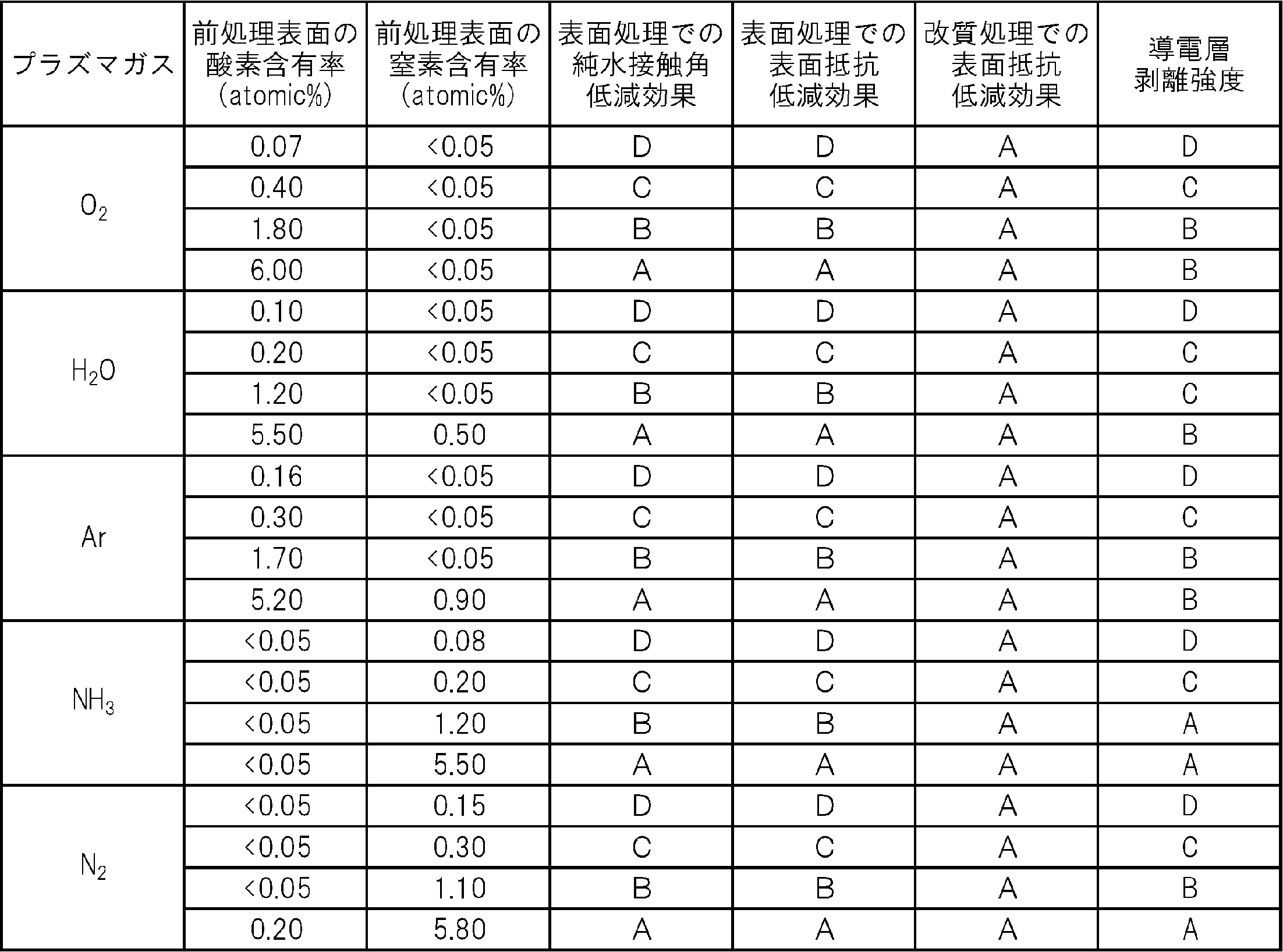
この試験結果から、酸素原子又は窒素原子の含有率が0.2atomic%以上の前処理表面を形成することにより、純水との接触角が十分低減され、その上に形成する導電層の表面抵抗を十分に低減でき、かつ導電層の剥離強度を向上できることが確認された。
また、改質処理での表面抵抗低減効果は、表面処理の種類及び程度にかかわらず良好であった。ただし、表には記載していないが、表面処理を行わず改質処理のみを行った場合には、表面抵抗の低減率が10%未満となった。このように、改質処理は、前処理表面と組み合わせることにより密着性を向上させる効果が大きくなる。
本発明に係るプリント配線板は、高周波信号を伝送する集積度の高い配線板として特に好適に使用される。
1,1a,1b,1c,1d,11 プリント配線板
2,2d 基材層
3 第1導電層
4,4b 第2導電層
5,5a,5b,5c ビアホール
6,6d 前処理表面
7 改質層
8,8a,8b,8c 下地導体層
9,9a,9b,9c 主導体層
10 補強材
12 第1基板
13 第2基板
14 接着剤
15 第1基材層
16 第1導電層
17 第2導電層
18 第2基材層
19 第3導電層
20 第1ビアホール
21 第2ビアホール
22 第1前処理表面
23 第2前処理表面
24 第1改質層
25 第2改質層
26 第1下地導体層
27 第1主導体層
28 第2下地導体層
29 第2主導体層
M めっき用マスク
2,2d 基材層
3 第1導電層
4,4b 第2導電層
5,5a,5b,5c ビアホール
6,6d 前処理表面
7 改質層
8,8a,8b,8c 下地導体層
9,9a,9b,9c 主導体層
10 補強材
12 第1基板
13 第2基板
14 接着剤
15 第1基材層
16 第1導電層
17 第2導電層
18 第2基材層
19 第3導電層
20 第1ビアホール
21 第2ビアホール
22 第1前処理表面
23 第2前処理表面
24 第1改質層
25 第2改質層
26 第1下地導体層
27 第1主導体層
28 第2下地導体層
29 第2主導体層
M めっき用マスク
Claims (7)
- フッ素樹脂を主成分とする基材層と、この基材層の一方の面に積層される第1導電層と、上記基材層の他方の面に積層される第2導電層と、
上記基材層と上記第1導電層及び第2導電層の少なくとも一方とを厚さ方向に貫通する接続孔に沿って形成され、上記第1導電層及び第2導電層を電気的に接続するビアホールと
を備えるプリント配線板であって、
上記接続孔における上記基材層の内周面の少なくとも一部に、酸素原子又は窒素原子の含有率が0.2atomic%以上の前処理表面を有するプリント配線板。 - 上記接続孔における基材層の内周面のうち少なくとも上記前処理表面の形成領域に、親水性有機官能基を有する改質層をさらに備える請求項1に記載のプリント配線板。
- 上記ビアホールが、上記接続孔の内周面に接する下地導体層と、この下地導体層の内周面に接する主導体層とを有する請求項1又は請求項2に記載のプリント配線板。
- 上記前処理表面の純水との接触角が90°以下である請求項1、請求項2又は請求項3に記載のプリント配線板。
- 上記ビアホールと基材層との間の剥離強度が1.0N/cm以上である請求項1から請求項4のいずれか1項に記載のプリント配線板。
- フッ素樹脂を主成分とする基材層と、この基材層の一方の面に積層される第1導電層と、上記基材層の他方の面に積層される第2導電層と、上記第1導電層及び第2導電層を電気的に接続するビアホールとを備えるプリント配線板の製造方法であって、
上記基材層と上記第1導電層及び第2導電層の少なくとも一方とを貫通する接続孔を形成する工程と、
上記接続孔における上記基材層の内周面の少なくとも一部に、酸素原子又は窒素原子の含有率が0.2atomic%以上の前処理表面を形成する工程と、
上記接続孔の内周面に下地導体層及び主導体層を積層して上記ビアホールを形成する工程と
を備えるプリント配線板の製造方法。 - 上記下地導体層が導電性材料の付着又は銅の無電解めっきにより形成される請求項6に記載のプリント配線板の製造方法。
Priority Applications (3)
| Application Number | Priority Date | Filing Date | Title |
|---|---|---|---|
| EP15795735.8A EP3148301B1 (en) | 2014-05-21 | 2015-05-12 | Printed wiring board and method for producing printed wiring board |
| US15/311,601 US9894765B2 (en) | 2014-05-21 | 2015-05-12 | Printed wiring board and method for producing printed wiring board |
| CN201580026987.7A CN106465550B (zh) | 2014-05-21 | 2015-05-12 | 印刷线路板以及印刷线路板的制造方法 |
Applications Claiming Priority (4)
| Application Number | Priority Date | Filing Date | Title |
|---|---|---|---|
| JP2014105713 | 2014-05-21 | ||
| JP2014-105713 | 2014-05-21 | ||
| JP2015091450A JP6601814B2 (ja) | 2014-05-21 | 2015-04-28 | プリント配線板及びプリント配線板の製造方法 |
| JP2015-091450 | 2015-04-28 |
Publications (1)
| Publication Number | Publication Date |
|---|---|
| WO2015178258A1 true WO2015178258A1 (ja) | 2015-11-26 |
Family
ID=54553931
Family Applications (1)
| Application Number | Title | Priority Date | Filing Date |
|---|---|---|---|
| PCT/JP2015/063679 Ceased WO2015178258A1 (ja) | 2014-05-21 | 2015-05-12 | プリント配線板及びプリント配線板の製造方法 |
Country Status (5)
| Country | Link |
|---|---|
| US (1) | US9894765B2 (ja) |
| EP (1) | EP3148301B1 (ja) |
| JP (1) | JP6601814B2 (ja) |
| CN (1) | CN106465550B (ja) |
| WO (1) | WO2015178258A1 (ja) |
Cited By (2)
| Publication number | Priority date | Publication date | Assignee | Title |
|---|---|---|---|---|
| CN109892022A (zh) * | 2016-09-01 | 2019-06-14 | Agc株式会社 | 布线基板及其制造方法 |
| JPWO2020071287A1 (ja) * | 2018-10-05 | 2021-09-02 | パナソニックIpマネジメント株式会社 | 銅張積層板、配線板、及び樹脂付き銅箔 |
Families Citing this family (13)
| Publication number | Priority date | Publication date | Assignee | Title |
|---|---|---|---|---|
| CN111263535A (zh) * | 2015-07-15 | 2020-06-09 | 印刷电路板公司 | 制造印刷电路板的方法 |
| CN108738241A (zh) * | 2017-04-20 | 2018-11-02 | 鹏鼎控股(深圳)股份有限公司 | 电路板的制作方法及其制得的电路板 |
| US10420208B2 (en) * | 2017-09-06 | 2019-09-17 | Microsoft Technology Licensing, Llc | Metal layering construction in flex/rigid-flex printed circuits |
| US20220153945A1 (en) * | 2017-09-29 | 2022-05-19 | Iteq Corporation | Polymer matrix composite, prepreg and printed circuit board for eliminating skew and fiber weave effect |
| CN109673111B (zh) * | 2017-10-13 | 2021-08-20 | 宏启胜精密电子(秦皇岛)有限公司 | 电路板的制作方法 |
| JP2019153661A (ja) * | 2018-03-02 | 2019-09-12 | ローム株式会社 | 接着構造体、及び半導体モジュール |
| JP7057689B2 (ja) * | 2018-03-16 | 2022-04-20 | 日本ピラー工業株式会社 | 積層板 |
| JP2022048105A (ja) * | 2020-09-13 | 2022-03-25 | 豊光社テクノロジーズ株式会社 | 樹脂基材の表面処理方法、導体被覆樹脂基材の製造方法、導波管の製造方法、及び回路基板又はアンテナの製造方法 |
| JP7514157B2 (ja) * | 2020-10-12 | 2024-07-10 | 日本メクトロン株式会社 | スルーホール形成方法およびフレキシブルプリント配線板用基板 |
| WO2022224866A1 (ja) * | 2021-04-22 | 2022-10-27 | 住友電気工業株式会社 | フレキシブルプリント回路基板及びフレキシブルプリント回路基板の製造方法 |
| TWI840797B (zh) * | 2022-04-29 | 2024-05-01 | 陳冠宇 | 電路板 |
| JPWO2023132246A1 (ja) * | 2022-01-04 | 2023-07-13 | ||
| JP2023145402A (ja) * | 2022-03-28 | 2023-10-11 | 国立大学法人岩手大学 | 積層体の製造方法、積層体、プリント回路、デバイス回路、および電気電子機器 |
Citations (3)
| Publication number | Priority date | Publication date | Assignee | Title |
|---|---|---|---|---|
| JPH0430594A (ja) * | 1990-05-28 | 1992-02-03 | Fujitsu Ltd | プリント配線板の親水化処理方法 |
| JP2000068642A (ja) * | 1998-08-25 | 2000-03-03 | Fujitsu Ltd | 多層回路基板の製造方法 |
| JP2000313963A (ja) * | 1999-04-28 | 2000-11-14 | Sumitomo Metal Ind Ltd | 樹脂のめっき方法 |
Family Cites Families (14)
| Publication number | Priority date | Publication date | Assignee | Title |
|---|---|---|---|---|
| US2897409A (en) * | 1954-10-06 | 1959-07-28 | Sprague Electric Co | Plating process |
| US4731156A (en) * | 1987-02-25 | 1988-03-15 | Itt Avionics, A Division Of Itt Corporation | Plasma processes for surface modification of fluoropolymers using ammonia |
| JPH1174651A (ja) * | 1997-03-13 | 1999-03-16 | Ibiden Co Ltd | プリント配線板及びその製造方法 |
| MY139405A (en) * | 1998-09-28 | 2009-09-30 | Ibiden Co Ltd | Printed circuit board and method for its production |
| US7514637B1 (en) * | 1999-08-06 | 2009-04-07 | Ibiden Co., Ltd. | Electroplating solution, method for fabricating multilayer printed wiring board using the solution, and multilayer printed wiring board |
| JP4075379B2 (ja) * | 2002-01-08 | 2008-04-16 | 株式会社デンソー | フッ素樹脂の表面処理方法およびフッ素樹脂を用いたプリント配線基板の製造方法 |
| US7485812B2 (en) * | 2002-06-27 | 2009-02-03 | Ppg Industries Ohio, Inc. | Single or multi-layer printed circuit board with improved via design |
| US6776827B2 (en) | 2002-09-23 | 2004-08-17 | Syed M. Hasan | Method and solution for treating fluorocarbon surfaces |
| US7743494B2 (en) * | 2008-01-11 | 2010-06-29 | Ppg Industries Ohio, Inc. | Process of fabricating a circuit board |
| CN101747490B (zh) * | 2008-12-19 | 2012-07-04 | 比亚迪股份有限公司 | 含氟树脂及其制备方法以及保形涂料和印刷线路板 |
| JP5587116B2 (ja) * | 2009-09-30 | 2014-09-10 | 京セラ株式会社 | 配線基板及び実装構造体 |
| JP5849308B2 (ja) * | 2011-08-31 | 2016-01-27 | 住友ゴム工業株式会社 | 表面改質フッ素樹脂フィルムの製造方法及び表面改質フッ素樹脂フィルム |
| JP5895573B2 (ja) | 2012-02-10 | 2016-03-30 | 住友電気工業株式会社 | プリント配線板用基材およびプリント配線板用基材の製造方法 |
| JP5711788B2 (ja) | 2013-07-25 | 2015-05-07 | 住友電気工業株式会社 | プリント配線板 |
-
2015
- 2015-04-28 JP JP2015091450A patent/JP6601814B2/ja active Active
- 2015-05-12 WO PCT/JP2015/063679 patent/WO2015178258A1/ja not_active Ceased
- 2015-05-12 CN CN201580026987.7A patent/CN106465550B/zh active Active
- 2015-05-12 US US15/311,601 patent/US9894765B2/en active Active
- 2015-05-12 EP EP15795735.8A patent/EP3148301B1/en active Active
Patent Citations (3)
| Publication number | Priority date | Publication date | Assignee | Title |
|---|---|---|---|---|
| JPH0430594A (ja) * | 1990-05-28 | 1992-02-03 | Fujitsu Ltd | プリント配線板の親水化処理方法 |
| JP2000068642A (ja) * | 1998-08-25 | 2000-03-03 | Fujitsu Ltd | 多層回路基板の製造方法 |
| JP2000313963A (ja) * | 1999-04-28 | 2000-11-14 | Sumitomo Metal Ind Ltd | 樹脂のめっき方法 |
Cited By (3)
| Publication number | Priority date | Publication date | Assignee | Title |
|---|---|---|---|---|
| CN109892022A (zh) * | 2016-09-01 | 2019-06-14 | Agc株式会社 | 布线基板及其制造方法 |
| JPWO2020071287A1 (ja) * | 2018-10-05 | 2021-09-02 | パナソニックIpマネジメント株式会社 | 銅張積層板、配線板、及び樹脂付き銅箔 |
| JP7445830B2 (ja) | 2018-10-05 | 2024-03-08 | パナソニックIpマネジメント株式会社 | 銅張積層板、配線板、及び樹脂付き銅箔 |
Also Published As
| Publication number | Publication date |
|---|---|
| JP6601814B2 (ja) | 2019-11-06 |
| US20170118837A1 (en) | 2017-04-27 |
| CN106465550A (zh) | 2017-02-22 |
| EP3148301B1 (en) | 2020-11-25 |
| EP3148301A4 (en) | 2017-09-27 |
| US9894765B2 (en) | 2018-02-13 |
| CN106465550B (zh) | 2019-05-14 |
| JP2016001728A (ja) | 2016-01-07 |
| EP3148301A1 (en) | 2017-03-29 |
Similar Documents
| Publication | Publication Date | Title |
|---|---|---|
| JP6601814B2 (ja) | プリント配線板及びプリント配線板の製造方法 | |
| US11364714B2 (en) | Fluororesin base material, printed wiring board, and circuit module | |
| JP6461532B2 (ja) | フッ素樹脂基材の製造方法及びプリント配線板の製造方法 | |
| JP6639775B2 (ja) | 樹脂フィルム、プリント配線板用カバーレイ、プリント配線板用基板及びプリント配線板 | |
| JP6809771B2 (ja) | フッ素樹脂基材、プリント配線板、及び回路モジュール | |
| KR102548004B1 (ko) | 수지 조성물 | |
| KR101920976B1 (ko) | 구리박, 캐리어박 부착 구리박, 및 구리 피복 적층판 | |
| CN105102678B (zh) | 表面处理铜箔及用表面处理铜箔得到的覆铜层压板 | |
| CN106103082A (zh) | 带有载体箔的铜箔、覆铜层压板及印刷线路板 | |
| JP6332787B2 (ja) | カバーレイ及びプリント配線板 | |
| JP2019104171A (ja) | 金属−樹脂積層体 | |
| JP6717835B2 (ja) | プリント配線板用基板、プリント配線板及びプリント配線板用基板の製造方法 | |
| WO2015053309A1 (ja) | フッ素樹脂基材、プリント配線板、及び回路モジュール | |
| JP6281762B2 (ja) | プリント配線板 | |
| JP6569936B2 (ja) | プリント配線板用基板 | |
| KR20230087692A (ko) | 저유전율 고분자 기판 및 이의 제조방법 |
Legal Events
| Date | Code | Title | Description |
|---|---|---|---|
| 121 | Ep: the epo has been informed by wipo that ep was designated in this application |
Ref document number: 15795735 Country of ref document: EP Kind code of ref document: A1 |
|
| WWE | Wipo information: entry into national phase |
Ref document number: 15311601 Country of ref document: US |
|
| NENP | Non-entry into the national phase |
Ref country code: DE |
|
| REEP | Request for entry into the european phase |
Ref document number: 2015795735 Country of ref document: EP |
|
| WWE | Wipo information: entry into national phase |
Ref document number: 2015795735 Country of ref document: EP |