WO2015198420A1 - Dispositif isolé au gaz - Google Patents
Dispositif isolé au gaz Download PDFInfo
- Publication number
- WO2015198420A1 WO2015198420A1 PCT/JP2014/066831 JP2014066831W WO2015198420A1 WO 2015198420 A1 WO2015198420 A1 WO 2015198420A1 JP 2014066831 W JP2014066831 W JP 2014066831W WO 2015198420 A1 WO2015198420 A1 WO 2015198420A1
- Authority
- WO
- WIPO (PCT)
- Prior art keywords
- coating
- insulating
- film
- conductor
- tank
- Prior art date
- Legal status (The legal status is an assumption and is not a legal conclusion. Google has not performed a legal analysis and makes no representation as to the accuracy of the status listed.)
- Ceased
Links
Images


Classifications
-
- H—ELECTRICITY
- H02—GENERATION; CONVERSION OR DISTRIBUTION OF ELECTRIC POWER
- H02G—INSTALLATION OF ELECTRIC CABLES OR LINES, OR OF COMBINED OPTICAL AND ELECTRIC CABLES OR LINES
- H02G5/00—Installations of bus-bars
- H02G5/06—Totally-enclosed installations, e.g. in metal casings
- H02G5/063—Totally-enclosed installations, e.g. in metal casings filled with oil or gas
-
- H—ELECTRICITY
- H01—ELECTRIC ELEMENTS
- H01F—MAGNETS; INDUCTANCES; TRANSFORMERS; SELECTION OF MATERIALS FOR THEIR MAGNETIC PROPERTIES
- H01F27/00—Details of transformers or inductances, in general
- H01F27/28—Coils; Windings; Conductive connections
- H01F27/32—Insulating of coils, windings, or parts thereof
- H01F27/321—Insulating of coils, windings, or parts thereof using a fluid for insulating purposes only
-
- H—ELECTRICITY
- H02—GENERATION; CONVERSION OR DISTRIBUTION OF ELECTRIC POWER
- H02B—BOARDS, SUBSTATIONS OR SWITCHING ARRANGEMENTS FOR THE SUPPLY OR DISTRIBUTION OF ELECTRIC POWER
- H02B13/00—Arrangement of switchgear in which switches are enclosed in, or structurally associated with, a casing, e.g. cubicle
- H02B13/02—Arrangement of switchgear in which switches are enclosed in, or structurally associated with, a casing, e.g. cubicle with metal casing
- H02B13/035—Gas-insulated switchgear
-
- H—ELECTRICITY
- H02—GENERATION; CONVERSION OR DISTRIBUTION OF ELECTRIC POWER
- H02G—INSTALLATION OF ELECTRIC CABLES OR LINES, OR OF COMBINED OPTICAL AND ELECTRIC CABLES OR LINES
- H02G5/00—Installations of bus-bars
- H02G5/06—Totally-enclosed installations, e.g. in metal casings
- H02G5/063—Totally-enclosed installations, e.g. in metal casings filled with oil or gas
- H02G5/065—Particle traps
Definitions
- the present invention relates to a gas insulating device in which a conductor as an energizing portion is accommodated in a grounded tank and an insulating gas is sealed in the tank.
- insulation performance is ensured by sealing an insulating gas in a space between a metal tank at ground potential and a conductor disposed inside the tank and to which a voltage is applied.
- the metal foreign object is charged due to the influence of the electric field generated from the energized conductor and can reciprocate in the radial direction in the tank, which may cause a decrease in withstand voltage. Therefore, it is necessary to suppress the behavior of the metal foreign matter in the tank.
- Patent Document 1 describes a gas insulating device in which a paint containing zinc oxide (ZnO) having non-linear resistance characteristics is applied to the inner surface of a tank.
- ZnO zinc oxide
- Patent Document 2 describes a technique for applying a non-linear resistance coating to a barrier insulator as a coating technique in a gas insulating device.
- JP 2010-207047 A Japanese Patent No. 4177628
- the coating film containing zinc oxide when the voltage is low, the coating film containing zinc oxide has high insulation, and it is metal from the inner surface of a tank. In order to block the movement of electric charges to the foreign matter, the same effect as that obtained when the above-mentioned insulating paint is applied to the inner surface of the tank is obtained.
- the coating film containing zinc oxide exhibits electrical conductivity when the voltage is high, and allows the movement of electric charge between the inner surface of the tank and the metallic foreign matter. Can be released from the metal foreign object to the tank in the film thickness direction.
- the coating film containing zinc oxide also allows the movement of charges having a polarity opposite to that of the conductor from the inner surface of the tank to the metal foreign object, it is difficult to suppress charging due to the movement of the charges. As a result, it becomes difficult to suppress the behavior of the metal foreign matter.
- Patent Document 2 is intended to suppress the progress of discharge and reliably confine the discharge in the gas space inside the barrier insulator, and to prevent the metallic foreign matter existing on the inner surface of the tank. It is different from the one intended to suppress the behavior.
- the present invention has been made in view of the above, and an object of the present invention is to provide a gas insulating device capable of suppressing the behavior of metal foreign matter.
- a gas insulating apparatus is provided with a metal tank that is grounded and filled with an insulating gas, and is disposed in the tank so that sealing treatment is performed.
- An alumite film is formed on the surface, a conductor to which a voltage is applied, an insulating part arranged on the inner surface of the tank, and a non-linear resistance material contained in the insulating material arranged on the insulating part And a non-linear resistance portion.
- the non-linear resistance part shows conductivity in the surroundings, and by releasing the charge from the metal foreign object to the non-linear resistance part, it becomes possible to suppress the behavior of the metal foreign object and relax the electric field around the metal foreign object, It is possible to suppress the occurrence of partial discharge.
- the alumite film that has been sealed is formed on the surface of the conductor, it is possible to suppress discharge from the surface of the conductor and to reduce the micro electric field on the surface of the conductor. Concentration can also be relaxed, and a reduction in withstand voltage due to the electrode area effect can be suppressed, and a gas insulation device with high insulation reliability can be applied.
- the withstand voltage performance can be improved, and the diameter of the tank can be reduced.
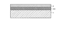
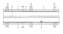
- FIG. 1 is a longitudinal sectional view showing a configuration of a gas insulating device according to Embodiment 1.
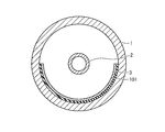
- FIG. FIG. 2 is an enlarged view of a portion A in FIG. 3 is a cross-sectional view taken along line BB in FIG.
- FIG. 4 is a diagram schematically showing a state in which electric charges escape from the metal foreign object toward the surface of the coating.
- FIG. 5 is a longitudinal sectional view showing a configuration of a conventional gas insulation device.
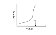
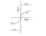
- FIG. 6 is a graph showing typical current-voltage characteristics of a non-linear resistance material.
- FIG. 7 is a graph comparing typical varistor characteristics of zinc oxide and silicon carbide.
- FIG. 8 is a diagram showing another example of the BB cross section in FIG. FIG.
- FIG. 9 is a diagram showing an example in which a coating is disposed on the entire inner surface of the tank.
- FIG. 10 is a longitudinal sectional view showing the configuration of the gas insulating device according to the second embodiment.
- FIG. 11 is an enlarged cross-sectional view of the surface of the conductor.
- FIG. 12 is a graph comparing the withstand voltage performance in sulfur hexafluoride gas when a conductor is not formed, when an alumite film is formed, and when an alumite film subjected to vapor sealing is formed.
- FIG. 13 is a diagram showing how the avalanche grows in the holes of the alumite film.
- FIG. 14 is a diagram showing the relationship between the pore diameter of the alumite coating and the withstand voltage performance.
- FIG. 15 is a cross-sectional view showing the relationship between the irregularities on the surface of the conductor that is the base of the anodized film and the film thickness of the anodized film.
- FIG. 1 is a longitudinal sectional view showing a configuration of a gas insulating device according to the present embodiment
- FIG. 2 is an enlarged view of a portion A in FIG. 1
- FIG. 3 is a BB transverse sectional view in FIG.
- the gas insulating device according to the present embodiment includes a metal tank 1 that is grounded and filled with an insulating gas, and a conductor that is a current-carrying portion disposed in the tank 1. 2, a coating 101 that is an insulating portion disposed on the inner surface of the tank 1, and a coating 3 that is a non-linear resistance portion disposed on the coating 101.
- the gas insulation apparatus which concerns on this Embodiment is an apparatus which comprises gas insulation switchgears, such as a bus-bar, a circuit breaker, a disconnecting switch, a grounding switch, an instrument current transformer, an instrument transformer.
- gas insulation switchgears such as a bus-bar, a circuit breaker, a disconnecting switch, a grounding switch, an instrument current transformer, an instrument transformer.
- this embodiment can be applied to a gas insulated switchgear.
- the tank 1 is made of, for example, a cylindrical container made of a grounded metal.
- a flange portion 1 a is provided at an end portion in the axial direction of the container constituting the tank 1.
- the tank 1 can be extended in the axial direction by connecting the flange portions 1a of the container.
- the tank 1 is disposed, for example, so that the axis of the tank 1 is horizontal. Or the tank 1 is arrange
- the tank 1 is filled with an insulating gas which is, for example, sulfur hexafluoride (SF 6 ) gas.
- SF 6 sulfur hexafluoride
- Conductor 2 is a conductor to which a voltage is applied, and a current flows therethrough.
- the conductor 2 extends, for example, along the axial direction of the tank 1.
- the conductor 2 is, for example, cylindrical or columnar.
- the conductor 2 is supported by an insulating spacer (not shown).
- the film 101 as the first film is an insulating film and is formed of an insulating material.
- the insulating material is, for example, a resin.
- the coating 101 is disposed on the lower half of the inner surface of the tank 1.
- the film 3 as the second film is a film in which a non-linear resistance material is contained in an insulating material.
- the insulating material is, for example, a resin.
- the nonlinear resistance material is, for example, silicon carbide (SiC). Since the coating 3 is isolated from the grounded tank 1 by the insulating coating 101, it is electrically floating.
- silicon carbide is known to exhibit non-linear resistance characteristics without firing. That is, silicon carbide exhibits insulation in a low voltage region or a low current region without firing, but has a low resistance in a high voltage region or a high current region. As will be described later, silicon carbide has a continuous transition between insulation and conductivity as compared to zinc oxide (ZnO). Silicon carbide is a wide band gap semiconductor having a larger band gap than silicon. Examples of the wide band gap semiconductor include gallium nitride and diamond in addition to silicon carbide.
- the filling rate of silicon carbide in the coating 3 can be in the range of 30% to 80%, for example, in terms of volume fraction. This is because, in order for the coating 3 to exhibit non-linear resistance characteristics, a filling amount that allows silicon carbide to come into contact with each other in the coating 3 is required.
- the lower limit of the filling amount is defined as the filling amount at which silicon carbide contacts with each other by percolation.
- the upper limit value of the filling amount is defined as the critical filling amount of the silicon carbide powder, and if the amount exceeding the critical filling amount is filled, the coating 3 becomes brittle, and therefore is determined from the condition for ensuring the strength of the coating 3.
- nonlinear resistance material included in the coating 3 may be a nonlinear resistance material other than silicon carbide, and may be, for example, zinc oxide, gallium nitride, or diamond.
- a minute metal foreign matter 4 is mixed in the tank 1 and is present on the coating 3, for example.
- the coatings 3, 101 are each a coating film formed by, for example, painting. That is, the coating 101 is formed by coating the inner surface of the tank 1 with, for example, an insulating paint mainly composed of a resin.
- the coating 3 is formed by, for example, coating the coating 101 with a non-linear resistance material containing an insulating coating mainly composed of a resin. Paint includes brush painting, spray painting, and electrostatic painting. Electrostatic coating is a coating that applies static electricity to powder and adheres to a target.
- either one or both of the coatings 3, 101 may be formed by a method other than painting.
- an insulating sheet as an insulating portion may be disposed on the inner surface of the tank 1.
- the insulating sheet is a sheet formed of an insulating material.
- a non-linear resistance sheet as a non-linear resistance portion may be disposed on the coating 101.
- the non-linear resistance sheet is a sheet formed by containing a non-linear resistance material in an insulating material.
- a sheet in which the coating 3 is formed on the insulating sheet by painting for example, may be disposed on the inner surface of the tank 1.
- the insulating portion and the non-linear resistance portion laminated on the inner surface of the tank 1 are not limited to the coating films 101 and 3, and may be any as long as they exhibit the insulating characteristics and the non-linear resistance characteristics, respectively.
- the non-linear resistance material in the coating 3 functions as a substantially insulating material.
- An insulating film 101 exists between the film 3 and the inner surface of the tank 1. Therefore, the movement of electric charge from the inner surface of the tank 1 to the metal foreign matter 4 on the coating 3 is blocked, and the electric charge having the opposite polarity to that of the conductor 2 is not stored in the metal foreign matter 4, so The suction force is greater than the weight of the metal foreign object 4 and the metal foreign object 4 does not float.
- the coating 101 under the coating 3 is insulative regardless of the magnitude of the electric field strength. For this reason, the charging of the metallic foreign matter 4 existing on the coating 3 is suppressed by the coating 3 becoming a charge escape field, while the metal is transferred from the inner surface of the tank 1 to the metallic foreign matter 4 due to the transfer of charges having a polarity opposite to that of the conductor 2. The charging of the foreign matter 4 is blocked by the coating 101, so that the electric attractive force due to the electric field generated from the conductor 2 is greater than the weight of the metallic foreign matter 4 and the metallic foreign matter 4 does not rise.
- the coating 3 out of the periphery of the metallic foreign matter 4 is present.
- the electric field concentration occurs on the side, the electric field strength increases, and the electric field on the side of the film 3 causes the film 3 to exhibit conductivity around the metal foreign matter 4.
- the coating 3 exhibits conductivity around the metal foreign object 4
- the charging of the metal foreign object 4 is suppressed as a charge escape field, and the electric field concentration around the metal foreign object 4 is alleviated.
- the occurrence of discharge is suppressed.
- the electric charge of the metal foreign matter 4 escapes in the surface direction of the coating 3 because the insulating coating 101 exists under the coating 3.
- FIG. 4 is a diagram schematically showing how electric charges escape from the metal foreign object 4 toward the surface of the coating 3.
- the same components as those in FIG. 1 are denoted by the same reference numerals.
- the conductive portion 3 a is generated in a part of the coating 3 due to the electric field around the metallic foreign material 4.
- the conductive portion 3 a is surrounded by an insulating portion 3 b that is another portion of the coating 3.
- the arrows indicate the direction of charge movement. As shown in FIG.
- a conductive portion 3a is generated in a part of the coating 3 in contact with the metallic foreign matter 4, and the electric charge of the metallic foreign matter 4 is within the conductive portion 3a. Is moved to the surface of the coating 3 to be uniform, and the charging of the metallic foreign matter 4 is suppressed, the electric field concentration is reduced, and the occurrence of partial discharge is suppressed. Note that the filling rate of the non-linear resistance material can be adjusted so that the conductive portion 3 a appears locally around the metal foreign material 4.
- the insulating film 101 is disposed on the inner surface of the tank 1, and the film 3 including the non-linear resistance material in the insulating material is disposed on the film 101.
- the coating 101 blocks the movement of electric charges from the inner surface of the tank 1 to the metallic foreign matter 4, while the electric field around the metallic foreign matter 4 in contact with the coating 3 has a high electric field strength.
- the coating 3 exhibits conductivity in the surroundings, and it is possible to suppress the behavior of the metallic foreign matter 4 by releasing the electric charge from the metallic foreign matter 4 to the coating 3, and the electric field around the metallic foreign matter 4 can be reduced. It is possible to suppress the occurrence of discharge.
- FIG. 5 is a longitudinal sectional view showing a configuration of a conventional gas insulation device.
- the same components as those in FIG. 1 are denoted by the same reference numerals.
- a coating film 100 is applied to the inner surface of the tank 1.
- the coating film 100 is made of a paint containing zinc oxide (see Patent Document 1). In the conventional configuration shown in FIG. 5, only one layer of the coating film 100 is applied.
- the zinc oxide in the coating film 100 functions as a substantial insulator.
- the insulating property is high, and the movement of charges from the inner surface of the tank 1 to the metal foreign matter 4 on the coating film 100 is blocked.
- the coating film 100 when the voltage applied to the conductor 2 is high, or when the strength of the electric field generated from the conductor 2 is large, if the metallic foreign matter 4 is present on the coating film 100, the coating film 100 out of the periphery of the metallic foreign matter 4 is present. Electric field concentration occurs on the side, the electric field strength increases, and the coating film 100 exhibits conductivity around the metallic foreign matter 4 due to the electric field on the coating film 100 side.
- the coating film 100 exhibits conductivity around the metal foreign object 4
- the movement of electric charge between the metal foreign object 4 and the inner surface of the tank 1 is allowed, and the electric charge of the metal foreign object 4 moves in the film thickness direction of the coating film 100. It will be escaped.
- the charge of the metal foreign matter 4 is released in the film thickness direction of the coating film 100, whereas in the present embodiment, the charge of the metal foreign matter 4 is released in the direction of the surface of the coating film 3. Is also different.
- FIG. 6 is a graph showing typical current-voltage characteristics of a non-linear resistance material.
- FIG. 7 is a graph comparing typical varistor characteristics of zinc oxide and silicon carbide. Zinc oxide exhibits non-linear resistance characteristics like silicon carbide, but as described below, the degree of non-linearity differs greatly between the two.
- Nonlinear resistance material is a low voltage indicating the resistance is large insulation, when the voltage exceeds a critical breakdown voltage V B, the resistance exhibits a drastically reduced conductivity.
- the film thickness of the coating 3 needs to be set so that charging of the metal foreign matter 4 can be suppressed in consideration of the applied voltage in the film thickness direction and the nonlinear resistance characteristics of the nonlinear resistance material.
- the non-linear resistance material contained in the coating 3 is zinc oxide, conductive regions and insulating regions are mixed on the coating 3 with respect to the same high electric field due to variations in the thickness of the coating 3. There is a possibility that the effect of suppressing the charging of the metallic foreign matter 4 is reduced. Therefore, when using zinc oxide as the non-linear resistance material, it is necessary to suppress variations in the film thickness of the coating 3.
- the film 3 when the non-linear resistance material contained in the film 3 is silicon carbide, the film 3 exhibits a gentle non-linear resistance characteristic as shown in FIG. Even if there is some variation in the film thickness of the coating 3, the coating 3 exhibits the same electrical characteristics as a whole, with only a slight difference in conductivity.
- the variation in the film thickness of the coating 3 has an effect on the charging suppression effect of the metal foreign matter 4 as compared with the case where zinc oxide is used as the non-linear resistance material. Is small, variation in film thickness is allowed, and workability in the manufacturing process of the coating 3 is improved.
- zinc oxide exhibits non-linear resistance characteristics when fired. Therefore, when the coating 3 is formed by painting, when the non-linear resistance material contained in the coating 3 is changed to zinc oxide, a mixture of fired zinc oxide powder mixed with a paint is applied, or zinc oxide It is necessary to fire the coating 3 after applying the contained paint, and in any case, a firing process is required before or after coating, and the number of manufacturing steps increases.
- silicon carbide exhibits non-linear resistance characteristics without firing. Therefore, when silicon carbide is used as the non-linear resistance material, there is no need to perform firing on silicon carbide, so that the number of manufacturing steps is reduced compared to the case where zinc oxide is used as the non-linear resistance material. There is.
- the coating 3 since the coating 3 is provided on the coating 101, the coating 3 can be disposed on the coating film using the existing tank 1 in which an insulating paint is applied to the inner surface of the tank 1. .
- the filler when forming the film 3 by painting, may or may not be added to the coating material containing the non-linear resistance material.
- the filler as an insulating material such as alumina or silica is intended to ensure the strength, and has no effect from the viewpoint of suppressing the behavior of the metal foreign matter 4.
- the coating 101 and the coating 3 are arranged on the lower half of the inner surface of the tank 1, but may be arranged on a part of the lower side of the inner surface of the tank 1.
- FIG. 8 is a diagram showing another example of the BB cross section in FIG.
- O indicates the center of the tank 1
- P indicates the lowermost part of the inner surface of the tank 1.
- the coating 101 and the coating 3 are disposed on the inner surface of the tank 1 in a certain angular range ⁇ including at least the lowermost portion P. Since the metallic foreign matter 4 tends to move downward due to its own weight, the coating 101 and the coating 3 are preferably disposed on at least a part of the lower side of the inner surface of the tank 1. In particular, since the metal foreign matter 4 tends to move toward the lowermost portion P due to its own weight, the coating 101 and the coating 3 are preferably disposed so as to cover at least the lowermost P of the inner surface of the tank 1.
- the present embodiment can also be realized by disposing the coating 101 and the coating 3 on a part or all of the upper side of the inner surface of the tank 1.
- the effect of form is obtained.
- the coating 101 and the coating 3 may be disposed on the entire inner surface of the tank 1.
- FIG. 9 shows an example in which the coating 101 and the coating 3 are arranged on the entire inner surface of the tank 1.
- FIG. FIG. 10 is a longitudinal sectional view showing the configuration of the gas insulation device according to the present embodiment.
- the gas insulating device according to the present embodiment is a metal tank 1 that is grounded and filled with an insulating gas, and is disposed in the tank 1, and the surface is sealed.
- An alumite film 6 is formed and a conductor 2 to which a voltage is applied is sandwiched between the flange portion 1a of the tank 1 and is attached to the insulating spacer 5 that supports the conductor 2, and is attached to the insulating spacer 5 side.
- An electric field relaxation shield 14 that covers a part of the conductor 2 and is formed with an alumite coating 16 that is sealed on the outer surface; and a coating 101 that is an insulating portion disposed on the inner surface of the tank 1; And a film 3 that is a non-linear resistance portion disposed on the film 101.
- the conductor 2 is made of aluminum, for example.
- the conductor 2 has a cylindrical shape, for example.
- an alumite film 6 that has been sealed for the purpose of further increasing the electric field strength of the dielectric breakdown is formed.
- the electric field relaxation shield 14 is made of aluminum, for example. On the outer surface of the electric field relaxation shield 14 is formed an alumite film 16 that has been sealed for the purpose of further increasing the dielectric breakdown electric field strength.
- the electric field relaxation shield 14 covers the periphery of the place where the conductor 2 is supported by the insulating spacer 5. A configuration in which the alumite coating 16 is not provided is also possible.
- the surface of the conductor 2 is uncoated.
- the surface protrusions On the surface of the conductor 2, there are a large number of surface protrusions due to irregularities of the ⁇ m level. Since the surface protrusions generate a discharge due to the electrons emitted from the surface protrusions, the surface protrusions cause a reduction in withstand voltage. In particular, as the surface area of the conductor 2 increases, the number of surface protrusions also increases and the probability of statistical discharge increases, so the breakdown field strength decreases.
- the conductor 2 has a coaxial cylindrical structure, an electric field gradient exists in the radial direction of the conductor 2, but the electric field is constant with respect to the circumferential direction and the axial direction of the conductor 2.
- the surface of the conductor 2 has the same electric field strength.
- an insulator starts discharge and breakdown is determined by the electric field strength.
- the dielectric breakdown electric field strength is the surface area of the conductor 2 due to the area effect caused by the surface protrusion of the conductor 2.
- the electrode area is as large as 100,000 mm 2 or more, and the breakdown field strength is significantly lower than that of a small-scale electrode area due to the area effect.
- insulating film on the surface of the conductor 2.
- This insulating film suppresses the field emission electrons generated from the surface protrusions of the conductor 2 and alleviates the electric field concentration caused by the surface protrusions, thereby suppressing the discharge and improving the withstand voltage.
- the insulating film is generally an alumite film by utilizing the fact that the conductor 2 is mainly made of aluminum (for example, see Japanese Patent Application Laid-Open No. 62-141909).
- the alumite film is formed by energizing the aluminum conductor 2 as an anode by immersing it in an electrolytic solution such as sulfuric acid aqueous solution, phosphoric acid aqueous solution or chromic acid aqueous solution in a treatment tank, and separately using the electrode immersed in this electrolytic solution as a cathode.
- An anodizing treatment by an electrolytic method is generally used. Accordingly, alumite is formed on the surface of the conductor 2 by oxidizing the surface of aluminum constituting the conductor 2, and a certain number of pores having a diameter of several hundreds of nanometers are formed in the alumite film during this oxidation process. When pores are present in the alumite coating, electrons emitted from the underlying conductor 2 are emitted through the pores, making it difficult to suppress discharge.
- the alumite film is subjected to a sealing process in order to close the holes present in the alumite film, and the surface of the conductor 2 is sealed. It is made to cover with the anodized film 6.
- the sealing treatment method is, for example, by vapor sealing.
- the conductor 2 or the electric field relaxation shield 14 on which the alumite film is formed is put in a kiln serving as a pressure vessel, and a treatment is performed by applying a steam pressure of, for example, 2 to 5 atmospheres with steam.
- a steam pressure of, for example, 2 to 5 atmospheres with steam.
- another sealing treatment method for example, there is a method using boiling water.
- a hydrate Al 2 O 3 .H 2 O
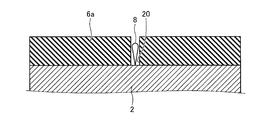
- FIG. 11 is an enlarged cross-sectional view of the surface of the conductor 2.
- an alumite film 6a is formed on the surface of the conductor 2, and a hole 20 is formed in the alumite film 6a.
- a hydrate film 7 is formed on the alumite film 6a by a sealing treatment, and the film 7 is also formed in the hole 20, the hole diameter of the hole 20 is reduced, and the hole 20 is sealed.
- the anodized film 6 is formed of an anodized film 6a and a hydrate film 7 formed on the anodized film 6a.
- FIG. 12 is a diagram comparing the withstand voltage performance in sulfur hexafluoride gas when the conductor 2 is not formed, when the alumite film 6a is formed, and when the vapor-sealed anodized film 6 is formed. It is.
- “No coating” indicates a case where no coating is formed on the conductor 2
- “Alumite” indicates a case where only the alumite coating 6 a is formed
- “Vapor-sealed anodized” indicates anodized anodized aluminum
- the case where the film 6 is formed is shown.
- the withstand voltage performance is shown as a relative value based on the case of “no coating”.
- the anodized coating 6 that has been subjected to the vapor sealing treatment has improved withstand voltage performance as compared with the case where no coating is applied or only the alumite coating 6a is formed.
- the alumite film 6 subjected to the sealing treatment is formed on the surface of the conductor 2, it is possible to suppress discharge from the surface of the conductor 2.
- the alumite film 6 having high insulation properties it is possible to alleviate the micro electric field concentration on the surface of the conductor 2, thereby suppressing a decrease in withstand voltage due to the electrode area effect, and gas insulation with high insulation reliability. Equipment can be applied.
- the alumite film 16 that has been subjected to the sealing treatment is formed also on the outer surface of the electric field relaxation shield 14, the alumite coating that has been subjected to the sealing treatment on the surface of the conductor 2. The same effect as when 6 is formed is produced.
- the anodized coating on which the outer surface of the other electric field relaxation shield is also sealed can be covered.
- the gas insulating device is a disconnector
- an alumite film that has been subjected to sealing treatment can be formed on the surface of the disconnector shield that covers the fixed contactor of the disconnector.
- the insulating film 101 is disposed on the inner surface of the tank 1, and the film 3 containing the nonlinear resistance material in the insulating material is disposed on the film 101.
- the same effects as in the first embodiment are obtained.
- the tank 1 side has a structure in which the coatings 101 and 3 are sequentially laminated on the inner surface of the tank 1, and the conductor 2 side has a structure in which anodizing that covers the surface of the conductor 2 is sealed. Therefore, the withstand voltage performance can be improved on both the tank 1 side and the conductor 2 side, and the diameter of the tank 1 can be reduced.
- FIG. 13 is a diagram showing how the avalanche grows in the pores of the alumite coating
- FIG. 14 is a diagram showing the relationship between the pore diameter of the alumite coating and the withstand voltage performance.
- an alumite film 6a is formed on the surface of the conductor 2, the alumite film 6a is not subjected to sealing treatment, and a hole 20 is present in the alumite film 6a.
- the hole 20 is present in the alumite coating 6 a, electron emission from the conductor 2 occurs through the hole 20.
- the electrons emitted from the conductor 2 are accelerated by the electric field, and the accelerated electrons collide with neutral molecules and ionize the molecules to generate new electrons, which are generated one after another.
- the resulting electrons lead to the growth of the avalanche 8.
- the avalanche 8 grows in a spindle shape in the advancing direction of the avalanche 8, and discharge starts when the tip of the avalanche 8 reaches the condition for transition to a streamer.
- the hole diameter of the hole 20 of the alumite film 6a is larger than the diameter of the tip of the electron avalanche 8
- the electron avalanche 8 continues to grow without colliding with the wall surface of the hole 20, and the electron avalanche 8 has a certain number of electrons.
- the avalanche 8 is transferred to a streamer and leads to dielectric breakdown.
- the diameter is the maximum diameter of the spindle-shaped avalanche 8.
- the advancing distance is the distance at which the avalanche 8 develops before reaching the condition where the tip of the avalanche 8 is transferred to the streamer
- the advancing distance is about 10 ⁇ m in the atmosphere, and pressurized sulfur hexafluoride If it is in gas, it becomes 100 nm or less.
- pressurized gas since the diameter of the avalanche 8 is smaller than the diameter of the normal alumite coating 6a that is not subjected to sealing treatment, the growth of the avalanche 8 due to the collision with the side wall of the hole 20 is not hindered.
- the avalanche 8 is transferred to a streamer after growth and discharge starts.
- the hole diameter of the alumite coating 6a is smaller than the diameter of the electron avalanche 8
- the growth of the electron avalanche 8 is inhibited by the collision with the side wall of the hole 20, thereby making it impossible to form a discharge due to the streamer transition.
- the withstand voltage performance is improved as shown in FIG.
- the pore diameter of the alumite may be suppressed to a diameter of the avalanche or less by sealing treatment.
- the sealing treatment is larger than the diameter of the avalanche 8 that is generated in the insulating gas. Sealing treatment is performed so that the pore diameter of the subsequent anodized coating 6 is reduced. That is, the alumite film 6 has a hydrate film 7 also formed in the hole 20 as shown in FIG. 11, so that the hole diameter of the hole 20 in which the film 7 is formed is larger than the diameter of the electron avalanche 8. Sealing processing is performed to reduce the size.
- FIG. 15 is a cross-sectional view showing the relationship between the irregularities on the surface of the conductor 2 that is the base of the alumite coating 6 and the film thickness of the alumite coating 6. As shown in FIG. 15, irregularities are formed on the surface of the conductor 2, and the alumite coating 6 is formed with a film thickness that fills the irregularities on the surface.
- the withstand voltage reduction phenomenon due to the area effect of the conductor 2 is caused by the supply of initial electrons emitted from the micro surface protrusions on the surface of the conductor 2 and the locally large potential gradient formed by the surface protrusions. This is due to the fact that a discharge is easily formed with an increase in surface area.
- the alumite film 6 is formed with a film thickness that fills the irregularities on the surface of the conductor 2. That is, the film thickness of the alumite film 6 is made larger than the maximum roughness of the irregularities on the surface of the conductor 2.
- the alumite film 6 is formed with a film thickness that fills the unevenness of the surface of the conductor 2, it is possible to suppress a decrease in withstand voltage due to the electrode area effect, and a gas with high insulation reliability. Insulated electrical equipment can be provided.
- the gas insulated device according to the present invention is suitable for a device constituting a gas insulated switchgear.
Landscapes
- Engineering & Computer Science (AREA)
- Power Engineering (AREA)
- Chemical & Material Sciences (AREA)
- Oil, Petroleum & Natural Gas (AREA)
- Installation Of Bus-Bars (AREA)
- Gas-Insulated Switchgears (AREA)
Abstract
Priority Applications (4)
| Application Number | Priority Date | Filing Date | Title |
|---|---|---|---|
| US15/308,657 US9972987B2 (en) | 2014-06-25 | 2014-06-25 | Gas insulation device |
| EP14895607.1A EP3163701B1 (fr) | 2014-06-25 | 2014-06-25 | Dispositif isolé au gaz |
| JP2014543683A JP5705384B1 (ja) | 2014-06-25 | 2014-06-25 | ガス絶縁機器 |
| PCT/JP2014/066831 WO2015198420A1 (fr) | 2014-06-25 | 2014-06-25 | Dispositif isolé au gaz |
Applications Claiming Priority (1)
| Application Number | Priority Date | Filing Date | Title |
|---|---|---|---|
| PCT/JP2014/066831 WO2015198420A1 (fr) | 2014-06-25 | 2014-06-25 | Dispositif isolé au gaz |
Publications (1)
| Publication Number | Publication Date |
|---|---|
| WO2015198420A1 true WO2015198420A1 (fr) | 2015-12-30 |
Family
ID=52986012
Family Applications (1)
| Application Number | Title | Priority Date | Filing Date |
|---|---|---|---|
| PCT/JP2014/066831 Ceased WO2015198420A1 (fr) | 2014-06-25 | 2014-06-25 | Dispositif isolé au gaz |
Country Status (4)
| Country | Link |
|---|---|
| US (1) | US9972987B2 (fr) |
| EP (1) | EP3163701B1 (fr) |
| JP (1) | JP5705384B1 (fr) |
| WO (1) | WO2015198420A1 (fr) |
Cited By (7)
| Publication number | Priority date | Publication date | Assignee | Title |
|---|---|---|---|---|
| US10043621B2 (en) | 2014-03-12 | 2018-08-07 | Mitsubishi Electric Corporation | Gas insulated switchgear |
| US10256611B2 (en) | 2014-07-10 | 2019-04-09 | Mitsubishi Electric Corporation | Gas insulated electrical apparatus and method of manufacturing gas insulated electrical apparatus |
| JP2020038927A (ja) * | 2018-09-05 | 2020-03-12 | 東芝インフラシステムズ株式会社 | モールド形静止誘導機器 |
| JP2020158812A (ja) * | 2019-03-26 | 2020-10-01 | アイシン軽金属株式会社 | 絶縁性陽極酸化皮膜の製造方法 |
| US11070039B2 (en) * | 2017-05-19 | 2021-07-20 | Hitachi, Ltd. | Insulation spacer and gas insulation shutoff apparatus using the insulation spacer |
| JP2022015800A (ja) * | 2020-07-10 | 2022-01-21 | 株式会社日立製作所 | ガス絶縁開閉装置 |
| US11888295B2 (en) | 2019-02-01 | 2024-01-30 | Mitsubishi Electric Corporation | Gas insulated apparatus |
Families Citing this family (5)
| Publication number | Priority date | Publication date | Assignee | Title |
|---|---|---|---|---|
| JP5710080B2 (ja) * | 2013-01-21 | 2015-04-30 | 三菱電機株式会社 | ガス絶縁開閉装置 |
| WO2016080018A1 (fr) * | 2014-11-20 | 2016-05-26 | 三菱電機株式会社 | Dispositif de commutation à isolation au gaz |
| JP6645706B2 (ja) * | 2016-02-17 | 2020-02-14 | 三菱電機株式会社 | ガス絶縁電気機器 |
| EP3239997A1 (fr) * | 2016-04-25 | 2017-11-01 | ABB Schweiz AG | Appareil ht et procédé de fabrication d'un tel appareil |
| JP7266687B2 (ja) * | 2018-12-31 | 2023-04-28 | ヒタチ・エナジー・スウィツァーランド・アクチェンゲゼルシャフト | 一体型のタンク脚部粒子トラップ |
Citations (1)
| Publication number | Priority date | Publication date | Assignee | Title |
|---|---|---|---|---|
| JP2010207047A (ja) * | 2009-03-06 | 2010-09-16 | Toshiba Corp | 密閉型絶縁装置 |
Family Cites Families (10)
| Publication number | Priority date | Publication date | Assignee | Title |
|---|---|---|---|---|
| US3389214A (en) * | 1963-08-20 | 1968-06-18 | Ohio Brass Co | Coated insulator |
| US3710002A (en) * | 1971-06-09 | 1973-01-09 | E Link | An under-ground vented non-metallic transformer assembly |
| JPS4831403A (fr) * | 1971-08-27 | 1973-04-25 | ||
| JPH0775445B2 (ja) * | 1985-12-13 | 1995-08-09 | 株式会社東芝 | ガス絶縁開閉装置 |
| JPH0529152U (ja) | 1992-08-07 | 1993-04-16 | イビデン株式会社 | 電子部品装置 |
| DE19500849A1 (de) | 1995-01-13 | 1996-07-18 | Abb Research Ltd | Elektrisches Bauteil |
| JP4177628B2 (ja) | 2002-09-30 | 2008-11-05 | 株式会社東芝 | 複合絶縁方式ガス絶縁開閉装置 |
| CN101497251A (zh) * | 2008-02-01 | 2009-08-05 | 深圳富泰宏精密工业有限公司 | 壳体 |
| CN101497250A (zh) * | 2008-02-01 | 2009-08-05 | 深圳富泰宏精密工业有限公司 | 壳体 |
| JP5411194B2 (ja) * | 2011-03-30 | 2014-02-12 | 三菱電機株式会社 | ガス絶縁電気機器の製造方法 |
-
2014
- 2014-06-25 EP EP14895607.1A patent/EP3163701B1/fr active Active
- 2014-06-25 JP JP2014543683A patent/JP5705384B1/ja active Active
- 2014-06-25 WO PCT/JP2014/066831 patent/WO2015198420A1/fr not_active Ceased
- 2014-06-25 US US15/308,657 patent/US9972987B2/en active Active
Patent Citations (1)
| Publication number | Priority date | Publication date | Assignee | Title |
|---|---|---|---|---|
| JP2010207047A (ja) * | 2009-03-06 | 2010-09-16 | Toshiba Corp | 密閉型絶縁装置 |
Cited By (10)
| Publication number | Priority date | Publication date | Assignee | Title |
|---|---|---|---|---|
| US10043621B2 (en) | 2014-03-12 | 2018-08-07 | Mitsubishi Electric Corporation | Gas insulated switchgear |
| US10256611B2 (en) | 2014-07-10 | 2019-04-09 | Mitsubishi Electric Corporation | Gas insulated electrical apparatus and method of manufacturing gas insulated electrical apparatus |
| US11070039B2 (en) * | 2017-05-19 | 2021-07-20 | Hitachi, Ltd. | Insulation spacer and gas insulation shutoff apparatus using the insulation spacer |
| JP2020038927A (ja) * | 2018-09-05 | 2020-03-12 | 東芝インフラシステムズ株式会社 | モールド形静止誘導機器 |
| JP7292839B2 (ja) | 2018-09-05 | 2023-06-19 | 東芝インフラシステムズ株式会社 | モールド形静止誘導機器 |
| US11888295B2 (en) | 2019-02-01 | 2024-01-30 | Mitsubishi Electric Corporation | Gas insulated apparatus |
| JP2020158812A (ja) * | 2019-03-26 | 2020-10-01 | アイシン軽金属株式会社 | 絶縁性陽極酸化皮膜の製造方法 |
| JP7257210B2 (ja) | 2019-03-26 | 2023-04-13 | アイシン軽金属株式会社 | 絶縁性陽極酸化皮膜の製造方法 |
| JP2022015800A (ja) * | 2020-07-10 | 2022-01-21 | 株式会社日立製作所 | ガス絶縁開閉装置 |
| JP7278997B2 (ja) | 2020-07-10 | 2023-05-22 | 株式会社日立製作所 | ガス絶縁開閉装置 |
Also Published As
| Publication number | Publication date |
|---|---|
| JP5705384B1 (ja) | 2015-04-22 |
| US20170149226A1 (en) | 2017-05-25 |
| EP3163701B1 (fr) | 2021-06-09 |
| EP3163701A1 (fr) | 2017-05-03 |
| EP3163701A4 (fr) | 2018-02-14 |
| US9972987B2 (en) | 2018-05-15 |
| JPWO2015198420A1 (ja) | 2017-04-20 |
Similar Documents
| Publication | Publication Date | Title |
|---|---|---|
| JP5705384B1 (ja) | ガス絶縁機器 | |
| JP5859142B2 (ja) | ガス絶縁電気機器 | |
| JP5710080B2 (ja) | ガス絶縁開閉装置 | |
| JP6067150B2 (ja) | ガス絶縁電気機器 | |
| KR20160081365A (ko) | 가스 절연 개폐기의 전극 장치 | |
| JP6645706B2 (ja) | ガス絶縁電気機器 | |
| JP2008271744A (ja) | ガス絶縁電気機器 | |
| JP6071209B2 (ja) | ガス絶縁開閉装置、及びガス絶縁母線 | |
| JP2016101080A (ja) | 絶縁スペーサ | |
| JP4940020B2 (ja) | ガス絶縁開閉装置 | |
| Van Der Born et al. | The influence of thin dielectric coatings on LI and AC breakdown strength in SF6 and dry air | |
| JP4291013B2 (ja) | 真空バルブ | |
| JP2019110010A (ja) | 真空バルブ | |
| EP3168947B1 (fr) | Dispositif électrique à isolation gazeuse et procédé de fabrication d'un dispositif électrique à isolation gazeuse | |
| JP7374668B2 (ja) | 電気機器 | |
| WO2020152952A1 (fr) | Appareillage à isolation gazeuse et son procédé de fabrication | |
| JP5395038B2 (ja) | ガス絶縁電気機器 | |
| KR101860439B1 (ko) | 가스 절연 개폐기의 전극 장치 | |
| Feng et al. | Improvement of surface flashover voltage of Vacuum Interrupter by surface coating | |
| JP2023554041A (ja) | 中電圧および/または高電圧用途のための電気開閉装置 | |
| Van Der Born et al. | Evaluation of AC and LI breakdown strength of electrodes with thick dielectric coatings in SF6 and dry air | |
| JPH03251014A (ja) | ガス絶縁母線 | |
| CN119678232A (zh) | 高压设备中的涂覆有源部件以及用于提高介电强度的方法 | |
| JPS63207010A (ja) | 貫通形変流器を装着したブツシング | |
| JP2016131415A (ja) | ガス絶縁開閉装置 |
Legal Events
| Date | Code | Title | Description |
|---|---|---|---|
| ENP | Entry into the national phase |
Ref document number: 2014543683 Country of ref document: JP Kind code of ref document: A |
|
| 121 | Ep: the epo has been informed by wipo that ep was designated in this application |
Ref document number: 14895607 Country of ref document: EP Kind code of ref document: A1 |
|
| WWE | Wipo information: entry into national phase |
Ref document number: 15308657 Country of ref document: US |
|
| REEP | Request for entry into the european phase |
Ref document number: 2014895607 Country of ref document: EP |
|
| WWE | Wipo information: entry into national phase |
Ref document number: 2014895607 Country of ref document: EP |
|
| NENP | Non-entry into the national phase |
Ref country code: DE |