WO2015198950A1 - 半導体装置及びその製造方法 - Google Patents
半導体装置及びその製造方法 Download PDFInfo
- Publication number
- WO2015198950A1 WO2015198950A1 PCT/JP2015/067513 JP2015067513W WO2015198950A1 WO 2015198950 A1 WO2015198950 A1 WO 2015198950A1 JP 2015067513 W JP2015067513 W JP 2015067513W WO 2015198950 A1 WO2015198950 A1 WO 2015198950A1
- Authority
- WO
- WIPO (PCT)
- Prior art keywords
- semiconductor layer
- type semiconductor
- layer
- semiconductor device
- electrode
- Prior art date
- Legal status (The legal status is an assumption and is not a legal conclusion. Google has not performed a legal analysis and makes no representation as to the accuracy of the status listed.)
- Ceased
Links
Images

Classifications
-
- H—ELECTRICITY
- H10—SEMICONDUCTOR DEVICES; ELECTRIC SOLID-STATE DEVICES NOT OTHERWISE PROVIDED FOR
- H10D—INORGANIC ELECTRIC SEMICONDUCTOR DEVICES
- H10D8/00—Diodes
- H10D8/50—PIN diodes
-
- H—ELECTRICITY
- H10—SEMICONDUCTOR DEVICES; ELECTRIC SOLID-STATE DEVICES NOT OTHERWISE PROVIDED FOR
- H10D—INORGANIC ELECTRIC SEMICONDUCTOR DEVICES
- H10D62/00—Semiconductor bodies, or regions thereof, of devices having potential barriers
- H10D62/10—Shapes, relative sizes or dispositions of the regions of the semiconductor bodies; Shapes of the semiconductor bodies
- H10D62/129—Cathode regions of diodes
-
- H—ELECTRICITY
- H10—SEMICONDUCTOR DEVICES; ELECTRIC SOLID-STATE DEVICES NOT OTHERWISE PROVIDED FOR
- H10D—INORGANIC ELECTRIC SEMICONDUCTOR DEVICES
- H10D62/00—Semiconductor bodies, or regions thereof, of devices having potential barriers
- H10D62/10—Shapes, relative sizes or dispositions of the regions of the semiconductor bodies; Shapes of the semiconductor bodies
- H10D62/13—Semiconductor regions connected to electrodes carrying current to be rectified, amplified or switched, e.g. source or drain regions
-
- H—ELECTRICITY
- H10—SEMICONDUCTOR DEVICES; ELECTRIC SOLID-STATE DEVICES NOT OTHERWISE PROVIDED FOR
- H10D—INORGANIC ELECTRIC SEMICONDUCTOR DEVICES
- H10D62/00—Semiconductor bodies, or regions thereof, of devices having potential barriers
- H10D62/80—Semiconductor bodies, or regions thereof, of devices having potential barriers characterised by the materials
- H10D62/83—Semiconductor bodies, or regions thereof, of devices having potential barriers characterised by the materials being Group IV materials, e.g. B-doped Si or undoped Ge
- H10D62/8303—Diamond
-
- H—ELECTRICITY
- H10—SEMICONDUCTOR DEVICES; ELECTRIC SOLID-STATE DEVICES NOT OTHERWISE PROVIDED FOR
- H10D—INORGANIC ELECTRIC SEMICONDUCTOR DEVICES
- H10D64/00—Electrodes of devices having potential barriers
- H10D64/01—Manufacture or treatment
- H10D64/011—Manufacture or treatment of electrodes ohmically coupled to a semiconductor
- H10D64/0111—Manufacture or treatment of electrodes ohmically coupled to a semiconductor to Group IV semiconductors
- H10D64/0114—Manufacture or treatment of electrodes ohmically coupled to a semiconductor to Group IV semiconductors to diamond, semiconducting diamond-like carbon or graphene
-
- H—ELECTRICITY
- H10—SEMICONDUCTOR DEVICES; ELECTRIC SOLID-STATE DEVICES NOT OTHERWISE PROVIDED FOR
- H10D—INORGANIC ELECTRIC SEMICONDUCTOR DEVICES
- H10D64/00—Electrodes of devices having potential barriers
- H10D64/111—Field plates
-
- H—ELECTRICITY
- H10—SEMICONDUCTOR DEVICES; ELECTRIC SOLID-STATE DEVICES NOT OTHERWISE PROVIDED FOR
- H10D—INORGANIC ELECTRIC SEMICONDUCTOR DEVICES
- H10D64/00—Electrodes of devices having potential barriers
- H10D64/20—Electrodes characterised by their shapes, relative sizes or dispositions
- H10D64/23—Electrodes carrying the current to be rectified, amplified, oscillated or switched, e.g. sources, drains, anodes or cathodes
-
- H—ELECTRICITY
- H10—SEMICONDUCTOR DEVICES; ELECTRIC SOLID-STATE DEVICES NOT OTHERWISE PROVIDED FOR
- H10D—INORGANIC ELECTRIC SEMICONDUCTOR DEVICES
- H10D8/00—Diodes
-
- H—ELECTRICITY
- H10—SEMICONDUCTOR DEVICES; ELECTRIC SOLID-STATE DEVICES NOT OTHERWISE PROVIDED FOR
- H10D—INORGANIC ELECTRIC SEMICONDUCTOR DEVICES
- H10D8/00—Diodes
- H10D8/01—Manufacture or treatment
- H10D8/051—Manufacture or treatment of Schottky diodes
-
- H—ELECTRICITY
- H10—SEMICONDUCTOR DEVICES; ELECTRIC SOLID-STATE DEVICES NOT OTHERWISE PROVIDED FOR
- H10D—INORGANIC ELECTRIC SEMICONDUCTOR DEVICES
- H10D8/00—Diodes
- H10D8/422—PN diodes having the PN junctions in mesas
Definitions
- Embodiments of the present invention relate to a semiconductor device and a method of manufacturing the same.
- Embodiments of the present invention provide a high breakdown voltage semiconductor device and a method of manufacturing the same.
- a semiconductor device includes an n-type semiconductor layer including diamond, a first electrode including a first portion, an intermediate layer, and a p-type semiconductor layer including diamond.
- the intermediate layer contains at least one of carbide, graphite, graphene and amorphous carbon.
- the carbide includes at least one of Ti, Si, Al, W, Ni, Cr, Ca, Li, Ru, Mo, Zr, Sr, Co, Rb, K, Cu, and Na.
- the intermediate layer is projected onto a plane perpendicular to a direction from the n-type semiconductor layer toward the first electrode and a first region provided between the first portion and the n-type semiconductor layer. And a second region provided around the first region and not overlapping the first portion and continuous with the first region.
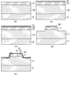
- FIG. 1 is a schematic cross-sectional view showing a semiconductor device according to a first embodiment.
- FIG. 2A to FIG. 2D are schematic cross-sectional views in order of processes, showing the method of manufacturing a semiconductor device according to the first embodiment. It is a schematic diagram which shows the characteristic of a semiconductor device. It is a typical sectional view showing a semiconductor device concerning a 2nd embodiment.
- FIG. 5A to FIG. 5E are schematic cross-sectional views in order of processes, showing the method of manufacturing a semiconductor device according to the second embodiment. It is a typical sectional view showing a semiconductor device concerning a 3rd embodiment.
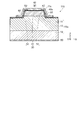
- FIG. 1 is a schematic cross-sectional view illustrating the semiconductor device according to the first embodiment.
- the semiconductor device 110 according to the present embodiment includes an n-type semiconductor layer 11, a p-type semiconductor layer 12, a first electrode 40, and an intermediate layer 30.
- the direction from the n-type semiconductor layer 11 toward the first electrode 40 is taken as a stacking direction (Z-axis direction).
- One direction perpendicular to the Z-axis direction is taken as the X-axis direction.
- a direction perpendicular to the Z-axis direction and the X-axis direction is taken as a Y-axis direction.
- the XY plane is a plane perpendicular to the stacking direction (Z-axis direction).
- the p-type semiconductor layer 12 is electrically connected to the n-type semiconductor layer 11.
- the electrically connected state includes a state in which the layers are in direct contact and a state in which another layer is inserted therebetween.
- the electrically connected state includes a state in which current can flow in at least one direction.
- the n-type semiconductor layer 11 and the p-type semiconductor layer 12 contain diamond.
- the semiconductor device 110 is a semiconductor device using diamond as a semiconductor layer.
- an intermediate semiconductor layer 13 is further provided.
- the intermediate semiconductor layer 13 is provided between the p-type semiconductor layer 13 and the n-type semiconductor layer 11 and contains diamond.
- the impurity concentration in the intermediate semiconductor layer 13 is lower than the impurity concentration in the p-type semiconductor layer 12.
- the impurity concentration in intermediate semiconductor layer 13 is lower than the impurity concentration in n-type semiconductor layer 11.
- the n-type semiconductor layer is an n + layer
- the p-type semiconductor layer is a p + layer
- the intermediate semiconductor layer 13 is ap ⁇ layer.
- the intermediate semiconductor layer 13 may be, for example, an intrinsic semiconductor.
- the pn junction comprises a stack of p-type and n-type layers.
- a layer having a low impurity concentration is provided between the p-type layer and the n-type layer, it is also included in the stack of pn junctions.
- a mesa structure is provided in the stacked body 10 u. That is, the n-type semiconductor layer 11 has the side surface 11s intersecting with the XY plane. In this example, the side surface 11s is inclined with respect to the Z-axis direction.
- the first electrode 40 is an ohmic electrode.
- the first electrode 40 includes a first portion 41.
- the first portion 41 of the first electrode 40 is a contact portion to the n-type semiconductor layer 11.
- the intermediate layer 30 includes a first region 31 and a second region 32.
- the first region 31 is provided between the first portion 41 and the n-type semiconductor layer 11.
- the first area 32 is provided around the first area 31 and does not overlap the first portion 41 when projected onto the XY plane.
- the second area 32 is continuous with the first area 31. In the embodiment, the first region 31 and the second region 32 are in contact with the n-type semiconductor layer 11.
- the intermediate layer 30 is conductive. A current flows between the first portion 41 of the first electrode 40 and the n-type semiconductor layer 11 via the first region 31 of the intermediate layer 30.
- the intermediate layer 30 contains at least one of carbide, graphite, graphene and amorphous carbon.
- the carbide is a carbide containing at least one of Ti, Si, Al, W, Ni, Cr, Ca, Li, Mo, Ru, Mo, Zr, Sr, Co, Rb, K, Cu and Na.
- the materials may be the same or different.
- the first electrode 40 further includes a second portion 42.
- the insulating layer 60 is further provided.
- the second portion 42 is provided around the first portion 41 when projected onto the XY plane.
- the second portion 42 is continuous with the first portion 41.
- the second portion 42 includes, for example, a pad portion provided around the contact portion.
- At least a portion of the insulating layer 60 is provided between the second portion 42 and the n-type semiconductor layer 11. Specifically, the insulating layer 60 is disposed between the second portion 42 and the second region 32.
- the second portion 42 of the first electrode 40 is provided to cover the side surface 11 s of the n-type semiconductor layer 11. That is, the first electrode 40 includes a portion 40s (for example, a part of the second portion 42) facing the side surface 11s of the n-type semiconductor layer 11.
- the insulating layer 60 extends between the side surface 11 s of the n-type semiconductor layer 11 and the above-mentioned opposing portion 40 s (a part of the second portion 42) of the first electrode 40. That is, the insulating layer 60 is provided to cover the side surface 11 s of the n-type semiconductor layer 11, and the first electrode 40 is provided on such an insulating layer 60.
- the insulating layer 60 functions as a protective layer. As described later, the second portion 42 and the insulating layer 60 may be omitted.
- the n-type semiconductor layer 11 is disposed between the first electrode 40 and the p-type semiconductor layer 12.
- the 2nd electrode 50 is further provided.
- the second electrode 50 is electrically connected to the p-type semiconductor layer 12.
- the n-type semiconductor layer 11 is disposed between the first electrode 40 and the second electrode 50.
- the p-type semiconductor layer 12 is disposed between the n-type semiconductor layer 11 and the second electrode 50.
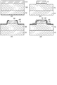
- FIG. 2A to FIG. 2D are schematic cross-sectional views in order of processes, illustrating the method for manufacturing a semiconductor device according to the first embodiment.
- an undoped intrinsic semiconductor diamond layer 13f to be an intermediate semiconductor layer 13 is formed on a p-type semiconductor layer 12 (for example, a p-type diamond substrate), and an n-type semiconductor layer is formed thereon.
- the n-type diamond layer 11 f to be 11 is formed.
- microwave plasma CVD Chemical Vapor Deposition
- a part of the undoped intrinsic semiconductor diamond layer 13f and a part of the n-type diamond layer 11f are removed to form a mesa structure.
- patterning and RIE reactive Ion Etching
- RIE Reactive Ion Etching
- the insulating layer 60 is formed.
- a silicon oxide film to be the insulating layer 60 is formed by, eg, CVD.
- a part of the silicon oxide film is removed by patterning and etching. Thereby, the insulating layer 60 is formed.
- the heat treatment is performed, for example, in the air.
- the temperature is, for example, 1000 ° C. or more and 1500 ° C. or less, for example, 1300 ° C.
- the time is 10 minutes or more and 60 minutes or less, for example, 30 minutes.
- a compound including Si contained in the insulating layer 60 and C (carbon) contained in the n-type semiconductor layer 11 is formed.
- a SiC layer is formed. This SiC layer becomes a part (second region 32) of the intermediate layer 30.
- the first electrode 40 is formed.
- a conductive film to be the first electrode 40 is formed.
- a laminated film of Ti / Pt / Au is used as the conductive film.
- Electron beam evaporation for example, is used to form the laminated film.
- the Ti film is in contact with the n-type semiconductor layer 11 not covered by the insulating layer 60.
- the conductive film is patterned. Thereby, the first electrode 40 is formed.
- annealing is performed.
- the annealing temperature is, for example, 500 ° C. or more and 700 ° C. or less, for example, 600 ° C.
- the annealing time is 10 minutes or more and 60 minutes or less, for example, 30 minutes.
- a TiC layer is formed by Ti of the above-mentioned conductive film and carbon of the n-type semiconductor layer 11. This TiC layer becomes a part (first region 31) of the intermediate layer 30.
- the semiconductor device 110 is formed by the above steps.
- boron is used as an impurity in the p-type semiconductor layer 12.
- the concentration of boron in the p-type semiconductor layer 12 is, for example, 1 ⁇ 10 20 cm ⁇ 3 or more and 1 ⁇ 10 21 cm ⁇ 3 or less, and for example, 5 ⁇ 10 20 cm ⁇ 3 .
- phosphorus is used as an impurity in the n-type semiconductor layer 11.
- the concentration of phosphorus in the n-type semiconductor layer 11 is, for example, 5 ⁇ 10 19 cm ⁇ 3 or more and 5 ⁇ 10 20 cm ⁇ 3 or less, and is, for example, 1 ⁇ 10 20 cm ⁇ 3 .
- the concentration of impurities in the intermediate semiconductor layer 13 is lower than the lower limit of detection in secondary ion mass spectrometry (SIMS), for example, less than 1 ⁇ 10 15 cm ⁇ 3 .
- SIMS secondary ion mass spectrometry
- a TiC layer is provided as the first region 31, and a SiC layer is provided as the second region 32.
- the first region 31 and the second region 32 function as an electric field relaxation layer.
- the rectification ratio at ⁇ 10 V is, for example, 1 ⁇ 10 10 or more.
- the forward current density at 10 V is, for example, 1000 A / cm 2 or more. No breakdown occurs even when the reverse voltage is 10 kV.
- a semiconductor device with high withstand voltage can be provided.
- Diamond is strong and has high thermal conductivity (20 W / cmK).
- the band gap energy in diamond is 5.5 eV, and diamond is a wide gap semiconductor.
- Diamond has a high carrier mobility, the electron mobility is about 4500cm 2 / Vsec, hole mobility is about 3800 cm 2 / Vsec.
- the breakdown field strength in diamond is high, and 10 MV / cm is expected.
- Diamond is expected to be applied to power devices which can operate even at high temperatures, high frequency (power) devices, ultraviolet light devices, electron emission sources, and the like.
- power device performance index carrier index
- diamond is expected to significantly improve the performance of power devices as compared to SiC and GaN.
- the reverse breakdown voltage is determined by the depletion layer (i.e., i layer) at the pn junction interface. For this reason, it is possible to make use of the high dielectric breakdown electric field inherent to diamond. Also for the forward current, a very high mobility can be obtained in the diamond i layer, so high conductivity can be expected even if the i layer is thickened. The contact resistance to the n-type layer is reduced by high concentration doping, and ohmic contact is possible.
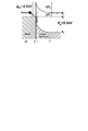
- FIG. 3 is a schematic view illustrating characteristics of the semiconductor device.
- FIG. 3 exemplifies the band state of diamond and metal.
- the Fermi level is strongly pinned at the surface of the n-type diamond (for example, the n-type semiconductor layer 11).
- n-type diamond for example, the n-type semiconductor layer 11
- a Schottky junction is formed immediately after depositing the metal film, but by forming TiC or the like by annealing, the pinning at the interface between the n-type diamond and the metal is relaxed. Be done. This makes it possible to reduce the contact resistance.
- the Fermi level at the diamond surface remains strongly pinned in the region of the n-type diamond other than immediately below the electrode. For this reason, when a voltage is applied, an electric field is generated between the electrode portion and the diamond surface (and its vicinity) around the electrode portion. And when a high voltage is applied, the electric field strength of this part becomes very high. This is considered to cause destruction. This phenomenon is considered to be a phenomenon that occurs specially in diamonds where Fermi level is strongly pinned.
- TiC is formed at the interface between the electrode immediately below the electrode and the diamond. For this reason, the pinning of the Fermi level of the surface of the n-type diamond immediately below the electrode is relaxed. On the other hand, at the surface of the n-type diamond where no electrode is provided, the Fermi level remains strongly pinned.
- Diamond has a higher surface state density and a lower dielectric constant than GaN. For this reason, it is difficult to reduce the electric field distribution. For this reason, in diamond, for example, a method different from that of a field plate or the like is required. For example, in diamond, it is considered effective to change the state of the surface.
- an intermediate layer is provided on the diamond surface around the n-side electrode end.
- a semiconductor device of high withstand voltage diamond can be provided.
- the embodiment provides a semiconductor device of diamond having high withstand voltage (for example, 10 kV or more) characteristics with good reproducibility.
- the intermediate layer (the second region 32 of the intermediate layer 30) is formed on the surface of the n-type diamond in the vicinity of the end of the n-side electrode (first electrode 40).
- the intermediate layer contains at least one layer of carbide, graphite, graphene and amorphous carbon.
- Such an intermediate layer may be provided between the n-type diamond and the insulating protective film (insulating layer 60).
- the embodiment it is possible to suppress the Fermi level pinning of the surface of the n-type diamond. Thereby, the electric field between the electrode and the n-type diamond around the electrode is suppressed, and the electric field concentration at the end of the electrode is alleviated.
- the n-type diamond immediately below the electrode is made TiC.
- it can be graphitized by annealing or ion implantation.
- a film including a carbo having a non-SP3 structure such as carbide or graphite is provided as the second region 32 of the intermediate layer 30 as the second region 32 of the intermediate layer 30, a film including a carbo having a non-SP3 structure such as carbide or graphite is provided. This can mitigate strong pinning of the Fermi level of the surface of the n-type diamond. The electric field generated between the electrode and the n-type diamond around the electrode can be relaxed. The breakdown voltage of the semiconductor device can be increased.
- a p ⁇ layer containing boron at a low concentration may be used as the intermediate semiconductor layer 13.
- the thickness (length in the Z-axis direction) of the intermediate layer 30 is 1 nanometer (nm) or more and 10 nm or less.
- Each of the thickness of the first region 31 and the thickness of the second region 32 is 1 nm or more and 10 nm or less. If the thickness is less than 1 nm, for example, the resistance of the intermediate layer 30 becomes excessively high. For example, the pinning of the interface between n-type diamond and metal becomes difficult to be alleviated. If the thickness is greater than 10 nm, for example, the intermediate layer 30 tends to be nonuniform.
- aluminum oxide for example, Al 2 O 3
- the second region 32 of the intermediate layer 30 is aluminum carbide.
- the first region 31 and the second region 32 of the intermediate layer 30 contain materials (elements) different from each other.
- the first region 31 contains an element (Ti in the above example) contained in the first electrode 40.
- the second region 32 contains an element (Si or Al in the above example) included in the insulating layer 60.
- the insulating layer 60 includes an oxide of silicon.
- the first region 31 includes TiC.
- the second region 32 contains SiC.
- the first region 31 of the intermediate layer 30 includes a compound including carbon contained in the n-type semiconductor layer 11 and an element contained in the first portion 41 of the first electrode 40.
- the insulating layer 60 at least one of silicon oxide, silicon nitride, aluminum oxide, aluminum nitride, zirconium oxide, hafnium oxide, and titanium oxide may be used.
- the same material is used in the first region 31 and the second region 32 of the intermediate layer 30.
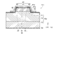
- FIG. 4 is a schematic cross-sectional view illustrating the semiconductor device according to the second embodiment.
- an intermediate layer 30 is provided between the n-type semiconductor layer 11 and the first electrode 40.
- the intermediate layer 30 includes a first region 31 and a second region 32.
- a portion located between the first portion 41 of the first electrode 40 and the n-type semiconductor layer 12 is a first region 31.
- the portion located between the insulating layer 60 and the n-type semiconductor layer 11 is the second region 32.
- the same material TiC or the like
- the other aspects are the same as those described in the first embodiment, and thus the description thereof is omitted.
- a boundary may not be observed between the first area 31 and the second area 32.
- the position of the outer edge (the boundary between the first portion 41 and the second portion 42) of the first portion 41 of the first electrode 40 corresponds to the position of the end of the insulating layer 60.
- the edge of the insulating layer 60 indicates the boundary between the first portion 41 and the second portion 42, and the boundary between the first region 31 and the second region 32.
- the second region 32 of the intermediate layer 30 is provided around the first portion 41 of the first electrode 40. This can mitigate strong pinning of the Fermi level of the surface of the n-type diamond. Then, the electric field generated between the electrode and the n-type diamond around the electrode can be relaxed. Also in the semiconductor device 111, high withstand voltage can be obtained.
- FIG. 5A to FIG. 5E are schematic cross-sectional views in order of processes, illustrating the method for manufacturing a semiconductor device according to the second embodiment. As shown in FIG. 5A, an undoped intrinsic semiconductor diamond layer 13f is formed on the p-type semiconductor layer 12, and an n-type diamond layer 11f is formed thereon.
- a metal film 70 is formed on the n-type diamond layer 11f.
- the metal film 70 for example, a laminated film of Ti / Pt / Au is formed by electron beam evaporation or the like.
- annealing is performed.
- the annealing is performed, for example, in air.
- the annealing temperature is, for example, 500 ° C. or more and 700 ° C. or less, for example, 600 ° C.
- the annealing time is 10 minutes or more and 60 minutes or less, for example, 30 minutes.
- the TiC layer 30f is formed by Ti contained in the Ti film and C (carbon) contained in the n-type diamond layer 11f.
- the TiC layer 30 f becomes the first region 31 and the second region 32 of the intermediate layer 30.
- the laminated film of Ti / Pt / Au is removed by acid treatment or the like.
- the above TiC layer 30f remains.
- a part of the TiC layer 30f, a part of the undoped intrinsic semiconductor diamond layer 13f, and a part of the n-type diamond layer 11f are removed to form a mesa structure. For example, patterning and RIE are performed. The intermediate semiconductor layer 13 and the n-type semiconductor layer 11 are formed.
- the insulating layer 60 is formed.
- the portion of the TiC layer 30 f located between the insulating layer 60 and the n-type semiconductor layer 11 is the second region 32 of the intermediate layer 30.
- the other part is the first area 31. Heat treatment may be performed if necessary.
- the semiconductor device 110 is formed by the above steps.
- the impurity and impurity concentration in the p-type semiconductor layer 12, the impurity and impurity concentration in the n-type semiconductor layer 11, and the impurity concentration in the intermediate semiconductor layer 13 are the same as those described in the first embodiment.
- TiC layers are provided as the first region 31 and the second region 32.
- the first region 31 and the second region 32 function as an electric field relaxation layer.
- the rectification ratio at ⁇ 10 V is, for example, 1 ⁇ 10 10 or more.
- the forward current density at 10 V is, for example, 1000 A / cm 2 or more. No breakdown occurs even when the reverse voltage is 10 kV. Thus, high withstand voltage can be obtained in the semiconductor device 111 as well.
- FIG. 6 is a schematic cross-sectional view illustrating the semiconductor device according to the third embodiment.
- an intermediate layer 30 is provided between the n-type semiconductor layer 11 and the first electrode 40.
- the intermediate layer 30 includes a first region 31 and a second region 32.
- the first electrode 41 is provided with a first portion 41.
- a portion located between the first portion 41 of the first electrode 40 and the n-type semiconductor layer 12 is a first region 31.
- a region not overlapping the first portion 41 when projected onto the XY plane is the second region 32.
- the second region 32 of the intermediate layer 30 is provided around the first portion 41 of the first electrode 40. This can mitigate strong pinning of the Fermi level of the surface of the n-type diamond. Then, the electric field generated between the electrode and the n-type diamond around the electrode can be relaxed. Also in the semiconductor device 112, high withstand voltage can be obtained.
- the same material may be used for the first region 31 and the second region 32, or different materials may be used.
- the outer edge of the first portion 41 corresponds to the boundary between the first region 31 and the second region 32.
- the fabrication of the semiconductor device 112 can be applied by modifying the method described in regard to the first embodiment or the second embodiment.
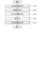
- FIG. 7 is a flowchart illustrating the method for manufacturing the semiconductor device according to the fourth embodiment.
- the n-type semiconductor layer 11 containing diamond is formed on the p-type semiconductor layer 12 containing diamond (step S110).
- the intermediate semiconductor layer 13 may be formed prior to the formation of the n-type semiconductor layer 11.
- the insulating layer 60 is formed on part of the n-type semiconductor layer 11 (step S120).
- Heat treatment is performed to form a first carbide layer (a second region 32 of the intermediate layer 30) (step S130).
- the first carbide layer contains carbon contained in the n-type semiconductor layer 11 and an element contained in the insulating layer 60.
- a film (film to be the first electrode 40) is formed on the n-type semiconductor layer 11 not covered by the insulating layer 60 (step S140).
- This film contains at least one of Ti, Si, Al, W, Ni, Cr, Ca, Li, Ru, Mo, Zr, Sr, Co, Rb, K, Cu and Na.
- the above film is processed to form a second carbide layer (the first region 31 of the intermediate layer 30) between the n-type semiconductor layer 11 not covered by the insulating layer 60 and the film (step S150).
- the second carbide layer includes at least one of Ti, Si, Al, W, Ni, Cr, Ca, Li, Mo, Ru, Mo, Zr, Sr, Co, Rb, K, Cu, and Na.
- the processing described in regard to FIG. 2A to FIG. 2D is performed.
- the semiconductor device 110 is formed.
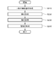
- FIG. 8 is a flowchart illustrating the method for manufacturing the semiconductor device according to the fifth embodiment.
- the n-type semiconductor layer 11 containing diamond is formed on the p-type semiconductor layer 12 containing diamond (step S210).
- the intermediate semiconductor layer 13 may be formed prior to the formation of the n-type semiconductor layer 11.
- a film (for example, the metal film 70 described in regard to FIG. 5B) is formed on the n-type semiconductor layer 11 (step S220).
- This film contains at least one of Ti, Si, Al, W, Ni, Cr, Ca, Li, Ru, Mo, Zr, Sr, Co, Rb, K, Cu and Na.
- the film is processed to form an intermediate layer 30 (step S230).
- the treatment includes, for example, heat treatment.
- the intermediate layer 30 includes carbides including at least any of the above Ti, Si, Al, W, Ni, Cr, Ca, Li, Mo, Ru, Mo, Zr, Sr, Co, Rb, K, Cu, and Na. .
- the above film (metal film 70) is removed as necessary.
- An electrode (first electrode 40) is formed on part of the intermediate layer 30 (step S240).
- the processing described in regard to FIGS. 5 (a) to 5 (e) is performed.
- the semiconductor device 111 can be formed.
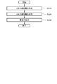
- FIG. 9 is a flowchart illustrating the method for manufacturing the semiconductor device according to the sixth embodiment.
- the n-type semiconductor layer 11 containing diamond is formed on the p-type semiconductor layer 12 containing diamond (step S310).
- the intermediate semiconductor layer 13 may be formed prior to the formation of the n-type semiconductor layer 11.
- the n-type semiconductor layer 11 is processed to form an intermediate layer 30 (step S320).
- the intermediate layer 30 contains at least one of carbide, graphite, graphene, and amorphous carbon. This carbide contains carbon contained in the n-type semiconductor layer 11.
- An electrode (first electrode 40) is formed on part of the intermediate layer 30 (step S330).
- the semiconductor device according to the embodiment can be formed.
- the process of step S320 includes, for example, at least one of heating of the n-type semiconductor layer 11, introduction of ions to the n-type semiconductor layer 11, and surface treatment of the n-type semiconductor layer 11.
- the intermediate layer 30 can be formed on the surface of the n-type semiconductor layer 11.
- the above ions at least one of Ti, Si, Al, W, Ni, Cr, Ca, Li, Mo, Ru, Mo, Zr, Sr, Co, Rb, K, Cu and Na can be used.
- the state to be formed on includes a state in which another element is formed between and formed on the other than the state to be formed in direct contact with.
- a high breakdown voltage semiconductor device and a method of manufacturing the same can be provided.
- vertical and parallel include not only strictly vertical and strictly parallel but also include, for example, variations in manufacturing processes, etc., and they may be substantially vertical and substantially parallel. Just do it.
Landscapes
- Electrodes Of Semiconductors (AREA)
Abstract
実施形態によれば、半導体装置は、ダイヤモンドを含むn形半導体層と、第1部分を含む第1電極と、中間層と、ダイヤモンドを含むp形半導体層と、を含む。前記中間層は、炭化物、グラファイト、グラフェン及びアモルファスカーボンの少なくともいずれかを含む。前記炭化物は、Ti、Si、Al、W、Ni、Cr、Ca、Li、Ru、Mo、Zr、Sr、Co、Rb、K、Cu及びNaの少なくともいずれかを含む。前記中間層は、前記第1部分と前記n形半導体層との間に設けられた第1領域と、前記n形半導体層から前記第1電極に向かう方向に対して垂直な平面に投影したときに前記第1領域の周りに設けられ前記第1部分と重ならず前記第1領域と連続した第2領域と、を含む。
Description
本発明の実施形態は、半導体装置及びその製造方法に関する。
ダイヤモンドを用いた半導体装置が提案されている。半導体装置において、耐圧が高いことが望まれる。
本発明の実施形態は、高耐圧の半導体装置及びその製造方法を提供する。
本発明の実施形態によれば、半導体装置は、ダイヤモンドを含むn形半導体層と、第1部分を含む第1電極と、中間層と、ダイヤモンドを含むp形半導体層と、を含む。前記中間層は、炭化物、グラファイト、グラフェン及びアモルファスカーボンの少なくともいずれかを含む。前記炭化物は、Ti、Si、Al、W、Ni、Cr、Ca、Li、Ru、Mo、Zr、Sr、Co、Rb、K、Cu及びNaの少なくともいずれかを含む。前記中間層は、前記第1部分と前記n形半導体層との間に設けられた第1領域と、前記n形半導体層から前記第1電極に向かう方向に対して垂直な平面に投影したときに前記第1領域の周りに設けられ前記第1部分と重ならず前記第1領域と連続した第2領域と、を含む。
以下に、本発明の各実施の形態について図面を参照しつつ説明する。
なお、図面は模式的または概念的なものであり、各部分の厚みと幅との関係、部分間の大きさの比率などは、必ずしも現実のものと同一とは限らない。また、同じ部分を表す場合であっても、図面により互いの寸法や比率が異なって表される場合もある。
なお、本願明細書と各図において、既出の図に関して前述したものと同様の要素には同一の符号を付して詳細な説明は適宜省略する。
なお、図面は模式的または概念的なものであり、各部分の厚みと幅との関係、部分間の大きさの比率などは、必ずしも現実のものと同一とは限らない。また、同じ部分を表す場合であっても、図面により互いの寸法や比率が異なって表される場合もある。
なお、本願明細書と各図において、既出の図に関して前述したものと同様の要素には同一の符号を付して詳細な説明は適宜省略する。
(第1の実施形態)
図1は、第1の実施形態に係る半導体装置を例示する模式的断面図である。
図1に表したように、本実施形態に係る半導体装置110は、n形半導体層11と、p形半導体層12と、第1電極40と、中間層30と、を含む。
図1は、第1の実施形態に係る半導体装置を例示する模式的断面図である。
図1に表したように、本実施形態に係る半導体装置110は、n形半導体層11と、p形半導体層12と、第1電極40と、中間層30と、を含む。
n形半導体層11から第1電極40に向かう方向を積層方向(Z軸方向)とする。Z軸方向に対して垂直な1つの方向をX軸方向とする。Z軸方向とX軸方向とに対して垂直な方向をY軸方向とする。X-Y平面は、積層方向(Z軸方向)に対して垂直な平面である。
p形半導体層12は、n形半導体層11と電気的に接続される。本明細書において、電気的に接続される状態は、直接接する状態と、間に別の層が挿入された状態と、を含む。電気的に接続される状態は、少なくとも1つの方向に電流が流れる状態が形成可能な状態を含む。
n形半導体層11及びp形半導体層12は、ダイヤモンドを含む。半導体装置110は、半導体層としてダイヤモンドを用いた半導体装置である。
この例では、中間半導体層13がさらに設けられている。中間半導体層13は、p形半導体層13とn形半導体層11との間に設けられ、ダイヤモンドを含む。中間半導体層13における不純物濃度は、p形半導体層12における不純物濃度よりも低い。中間半導体層13における不純物濃度は、n形半導体層11における不純物濃度よりも低い。
n形半導体層は、n+層であり、p形半導体層は、p+層である。中間半導体層13は、p-層である。または、中間半導体層13は、例えば、真性半導体でも良い。
これらの半導体層は、pn接合を有する積層体10uに含まれる。実施形態において、pn接合は、p形層及びn形層の積層体を含む。実施形態において、p形層とn形層との間に、不純物濃度が低い層が設けられる場合も、pn接合の積層体に含まれる。
この例では、積層体10uにおいて、メサ構造が設けられている。すなわち、n形半導体層11は、X-Y平面と交差する側面11sを有している。この例では、側面11sは、Z軸方向に対して傾斜している。
第1電極40とn形半導体層11との間に電流が流れる。第1電極40は、オーミック電極である。第1電極40は、第1部分41を含む。第1電極40の第1部分41は、n形半導体層11に対するコンタクト部分である。
中間層30は、第1領域31と、第2領域32と、を含む。第1領域31は、第1部分41とn形半導体層11との間に設けられる。第1領域32は、X-Y平面に投影したときに、第1領域31の周りに設けられ、第1部分41と重ならない。第2領域32は、第1領域31と連続している。実施形態において、第1領域31及び第2領域32は、n形半導体層11と接する。
中間層30は、導電性である。中間層30のうちの第1領域31を介して、第1電極40の第1部分41と、n形半導体層11と、の間に、電流が流れる。
中間層30は、炭化物、グラファイト、グラフェン及びアモルファスカーボンの少なくともいずれかを含む。この炭化物は、Ti、Si、Al、W、Ni、Cr、Ca、Li、Ru、Mo、Zr、Sr、Co、Rb、K、Cu及びNaの少なくともいずれかを含む炭化物である。
後述するように、中間層30の第1領域31と第2領域32とにおいて、材料は同じでも良く、異なっても良い。
この例では、第1電極40は、第2部分42をさらに含む。そして、絶縁層60がさらに設けられている。第2部分42は、X-Y平面に投影したときに、第1部分41の周りに設けられる。第2部分42は、第1部分41と連続している。第2部分42は、例えば、コンタクト部分の周りに設けられるパッド部分を含む。
絶縁層60の少なくとも一部は、第2部分42とn形半導体層11との間に設けられる。具体的には、絶縁層60は、第2部分42と第2領域32との間に配置される。
この例では、第1電極40のうちの第2部分42は、n形半導体層11の側面11sを覆うように設けられている。すなわち、第1電極40は、n形半導体層11の側面11sに対向する部分40s(例えば第2部分42の一部)を含む。絶縁層60は、n形半導体層11の側面11sと、第1電極40の上記の対向する部分40s(第2部分42の一部)との間に延在している。すなわち、絶縁層60が、n形半導体層11の側面11sを覆うように設けられ、このような絶縁層60の上に第1電極40が設けられる。絶縁層60でn形半導体層11の側面11sを覆うことで、例えば、信頼性が向上する。絶縁層60は、保護層として機能する。
後述するように、第2部分42及び絶縁層60は、省略しても良い。
後述するように、第2部分42及び絶縁層60は、省略しても良い。
この例では、第1電極40とp形半導体層12との間にn形半導体層11が配置される。そして、第2電極50がさらに設けられている。第2電極50は、p形半導体層12と電気的に接続される。第1電極40と第2電極50との間に、n形半導体層11が配置される。n形半導体層11と第2電極50との間に、p形半導体層12が配置される。
以下、半導体装置110の製造方法の例について説明する。
図2(a)~図2(d)は、第1の実施形態に係る半導体装置の製造方法を例示する工程順模式的断面図である。
図2(a)に示すように、p形半導体層12(例えばp形ダイヤモンド基板)の上に、中間半導体層13となるアンドープ真性半導体ダイヤモンド層13fを形成し、その上に、n形半導体層11となるn形ダイヤモンド層11fを形成する。これらの層の形成には、例えば、マイクロ波プラズマCVD(Chemical Vapor Deposition)法が用いられる。
図2(a)~図2(d)は、第1の実施形態に係る半導体装置の製造方法を例示する工程順模式的断面図である。
図2(a)に示すように、p形半導体層12(例えばp形ダイヤモンド基板)の上に、中間半導体層13となるアンドープ真性半導体ダイヤモンド層13fを形成し、その上に、n形半導体層11となるn形ダイヤモンド層11fを形成する。これらの層の形成には、例えば、マイクロ波プラズマCVD(Chemical Vapor Deposition)法が用いられる。
図2(b)に示すように、アンドープ真性半導体ダイヤモンド層13fの一部、及び、n形ダイヤモンド層11fの一部を除去して、メサ構造を形成する。これらの除去には、例えば、パターニングとRIE(Reactive Ion Etching)が用いられる。これにより、中間半導体層13及びn形半導体層11が形成される。
図2(c)に示すように、絶縁層60を形成する。例えば、絶縁層60となるシリコン酸化膜を例えばCVDにより形成する。パターニングとエッチングによりシリコン酸化膜の一部を除去する。これにより、絶縁層60が形成される。
この後、熱処理を行う。熱処理は、例えば、空気中で行われる。温度は、例えば1000℃以上1500℃以下であり、例えば、1300℃である。時間は、10分以上60分以下であり、例えば、30分である。この熱処理により、n形半導体層11のうちの絶縁層60に接する部分が、変化する。例えば、絶縁層60に含まれるSiと、n形半導体層11に含まれるC(炭素)と、を含む化合物が形成される。例えば、SiC層が形成される。このSiC層が、中間層30の一部(第2領域32)となる。
図2(d)に示すように、第1電極40を形成する。例えば、第1電極40となる導電膜を形成する。導電膜には、例えば、Ti/Pt/Auの積層膜が用いられる。積層膜の形成には、例えば、電子ビーム蒸着が用いられる。Ti膜が、絶縁層60に覆われていないn形半導体層11に接する。この導電膜をパターニングする。これにより、第1電極40が形成される。
この後、アニールを行う。アニールの温度は、例えば500℃以上700℃以下であり、例えば600℃である。アニールの時間は、10分以上60分以下であり、例えば30分である。このアニールにより、上記の導電膜のTiと、n形半導体層11の炭素と、によりTiC層が形成される。このTiC層は、中間層30の一部(第1領域31)となる。上記の工程により、半導体装置110が形成される。
p形半導体層12における不純物として、例えば、ホウ素が用いられる。p形半導体層12におけるホウ素の濃度は、例えば、1×1020cm-3以上1×1021cm-3以下であり、例えば、5×1020cm-3である。n形半導体層11における不純物として、例えば、リンが用いられる。n形半導体層11におけるリンの濃度は、例えば、5×1019cm-3以上5×1020cm-3以下であり、例えば、1×1020cm-3である。この例では、中間半導体層13における不純物の濃度は、2次イオン質量分析(SIMS)における検出下限よりも低く、例えば、1×1015cm-3未満である。
半導体装置110において、第1領域31としてTiC層が設けられ、第2領域32としてSiC層が設けられる。第1領域31及び第2領域32は、電界緩和層として機能する。
半導体装置110の電流-電圧特性(I-V特性)において、±10Vにおける整流比は、例えば、1×10¹⁰以上である。10Vにおける順方向電流密度は、例えば、1000A/cm2以上である。逆方向の電圧が10kVのときにおいても、ブレークダウンは生じない。
実施形態に係る半導体装置110によれば、高耐圧の半導体装置が提供できる。
ダイヤモンドは、強固で、高熱伝導率(20W/cmK)である。ダイヤモンドにおけるバンドギャップエネルギーは、5.5eVであり、ダイヤモンドは、ワイドギャップ半導体である。ダイヤモンドは、高キャリア移動度を有し、電子移動度は、約4500cm2/Vsecであり、ホール移動度は、約3800cm2/Vsecである。ダイヤモンドにおける破壊電界強度は高く、10MV/cmが期待される。ダイヤモンドは、高温でも動作可能なパワーデバイス、高周波(パワー)デバイス、紫外光デバイス、または、電子放出源等への応用が期待される。パワーデバイスの性能指数(バリガ指数)の比較からわかるように、ダイヤモンドは、SiC及びGaNに比べて、パワーデバイスの性能を大きく向上させると期待される。
これまでにダイヤモンドを用いたショットキー接合を有するダイオード、トランジスタの検討が行われている。しかしながら、ショットキー障壁高さによって耐圧の限界が制限される。このため、10kV以上の耐圧を得ることは困難である。
一方、バイポーラ型の伝導機構を有するpinダイオードにおいては、逆方向耐圧は、pn接合界面の空乏層(すなわちi層)で決まる。このため、ダイヤモンド本来の高い絶縁破壊電界を活かすことが可能である。順方向電流についても、ダイヤモンドi層において非常に高い移動度が得られることから、i層を厚くしても高い伝導度が期待できる。n形層へのコンタクト抵抗は高濃度ドーピングにより低減され、オーミックコンタクトが可能である。
しかしながら、pinダイオードでは、発光素子を目的とした報告がほとんどであり、逆方向耐圧は、ダイヤモンドに本来期待される値に比べて非常に小さい。
ショットキーダイオードでは、電極端に電界が集中することから、耐圧向上のために、フィールドプレートやガードリングなどの電界集中緩和構造について検討されている。しかしながら、pinダイオードは、通常、pn界面に最大電界が印加され、特に接合端での電界集中が問題となることから、電界緩和構造は電極端ではなくpn接合端のJTE構造(接合終端構造)について検討されている。
ダイヤモンドのpinダイオードにおいて、3MV/cmを越える大きな電界強度がドリフト層に印加されるような電圧で、pn接合端での降伏よりも先に電極端が破壊されてしまうことがわかった。これは、ダイヤモンド特有の表面状態に起因すると考えられる。
図3は、半導体装置の特性を例示する模式図である。
図3は、ダイヤモンドと金属とにおけるバンド状態を例示している。
図3に示すように、n形ダイヤモンド(例えばn形半導体層11)の表面において、フェルミレベルが強固にピニングしている。電極(金属)直下のn形ダイヤモンドにおいて、金属膜を堆積した直後ではショットキー接合が形成されるが、アニールにより、TiCなどを形成することで、n形ダイヤモンドと金属との界面のピニングが緩和される。これにより、接触抵抗を小さくすることが可能である。
図3は、ダイヤモンドと金属とにおけるバンド状態を例示している。
図3に示すように、n形ダイヤモンド(例えばn形半導体層11)の表面において、フェルミレベルが強固にピニングしている。電極(金属)直下のn形ダイヤモンドにおいて、金属膜を堆積した直後ではショットキー接合が形成されるが、アニールにより、TiCなどを形成することで、n形ダイヤモンドと金属との界面のピニングが緩和される。これにより、接触抵抗を小さくすることが可能である。
一方、n形ダイヤモンドのうちの電極直下以外の領域においては、ダイヤモンド表面でのフェルミレベルが強くピニングされたままである。このため、電圧を印加したときに、電極部と、電極部の周辺のダイヤモンド表面(及びその近傍)と、の間に電界が生じる。そして、高電圧を印加した場合には、この部分の電界強度が非常に高くなる。これにより、破壊が起こると考えられる。この現象は、フェルミレベルが強固にピニングするダイヤモンドにおいて特別に生じる現象であると考えられる。
例えば、オーミック電極としてTiを用いた場合、電極直下の電極と、ダイヤモンドとの間の界面には、TiCが形成される。このため、電極直下のn形ダイヤモンドの表面のフェルミレベルのピニングは緩和されている。一方、電極が設けられない部分のn形ダイヤモンドの表面においては、フェルミレベルは強固にピニングされたままである。
ダイヤモンドにおいては、GaNに比べて表面準位密度が高く、誘電率が低い。このため、電界分布が緩和されにくい。このため、ダイヤモンドにおいては、例えば、フィールドプレートなどとは異なる方法が要求される。例えば、ダイヤモンドにおいては、表面の状態を変えることが有効であると考えられる。
実施形態においては、n側電極端の周囲のダイヤモンド表面に中間層を設ける。これにより、高耐圧のダイヤモンドの半導体装置を提供できる。実施形態は、高耐圧(例えば10kV以上)の特性を持つダイヤモンドの半導体装置を再現良く提供する。
実施形態においては、例えば、ダイヤモンドpn接合を有する半導体装置において、n側電極(第1電極40)の端の近傍のn形ダイヤモンドの表面に、中間層(中間層30の第2領域32)を設ける。この中間層は、炭化物、グラファイト、グラフェン、及び、アモルファスカーボンの少なくともいずれかの層を含む。このような中間層を、n形ダイヤモンドと絶縁保護膜(絶縁層60)との間に設けても良い。
実施形態によれば、n形ダイヤモンドの表面のフェルミレベルのピニングを抑制できる。これにより、電極と、電極周囲のn形ダイヤモンドと、の間の電界を抑制し、電極の端の電界集中が緩和される。
カーバイドを電極とn形ダイヤモンドとの間に設けると、接触抵抗が小さくなる。カーバイドを電極とn形ダイヤモンドとの間に設けることで、フェルミレベルのピニングを抑制できる。
例えば、電極直下のn形ダイヤモンドをTiC化する。例えば、アニールまたはイオン注入などによって、グラファイト化することができる。
例えば、中間層30の第2領域32として、カーバイドまたはグラファイトなどの非SP3構造を有するカーボを含む膜を設ける。これにより、n形ダイヤモンドの表面のフェルミレベルの強固なピニングを緩和できる。電極と、電極周辺のn形ダイヤモンドと、の間に生じる電界を緩和することができる。半導体装置の耐圧を高くすることができる。
実施形態において、中間半導体層13として、低濃度でホウ素を含むp-層を用いても良い。
実施形態において、中間層30の厚さ(Z軸方向の長さ)は、1ナノメートル(nm)以上10nm以下である。第1領域31の厚さ及び第2領域32の厚さのそれぞれは、1nm以上10nm以下である。厚さが、1nmよりも薄いと、例えば、中間層30の抵抗が過度に高くなる。例えば、n形ダイヤモンドと金属との界面のピニングが緩和され難くなる。厚さが10nmよりも厚いと、例えば、中間層30が不均一になり易い。
実施形態において、絶縁層60として、例えば、酸化アルミニウム(例えば、Al2O3)などを用いても良い。この場合、例えば、中間層30の第2領域32は、炭化アルミニウムとなる。
半導体装置110においては、中間層30の第1領域31と第2領域32とは、互いに異なる材料(元素)を含む。上記の例では、第1領域31は、第1電極40に含まれる元素(上記の例ではTi)を含む。第2領域32は、絶縁層60に含まれる元素(上記の例ではSiまたはAl)を含む。
例えば、絶縁層60は、シリコンの酸化物を含む。このとき、例えば、第1領域31は、TiCを含む。第2領域32は、SiCを含む。例えば、中間層30の第1領域31は、n形半導体層11に含まれる炭素と、第1電極40の第1部分41に含まれる元素と、を含む化合物を含む。
実施形態において、絶縁層60として、シリコン酸化物、シリコン窒化物、アルミニウム酸化物、アルミニウム窒化物、ジルコニウム酸化物、ハフニウム酸化物、及び、チタン酸化物の少なくともいずれかを用いても良い。
(第2の実施形態)
本実施形態においては、中間層30の第1領域31と第2領域32において、同じ材料が用いられる。
本実施形態においては、中間層30の第1領域31と第2領域32において、同じ材料が用いられる。
図4は、第2の実施形態に係る半導体装置を例示する模式的断面図である。
図4に示すように、本実施形態に係る半導体装置111においても、n形半導体層11と第1電極40との間に中間層30が設けられている。中間層30は、第1領域31と第2領域32とを含む。第1電極40の第1部分41と、n形半導体層12と、の間に位置する部分が、第1領域31となる。絶縁層60とn形半導体層11との間に位置する部分が、第2領域32となる。第1領域31と第2領域32とには、同じ材料(TiCなど)が用いられる。これ以外は、第1の実施形態に関して説明したのと同様とすることができるので、説明を省略する。
図4に示すように、本実施形態に係る半導体装置111においても、n形半導体層11と第1電極40との間に中間層30が設けられている。中間層30は、第1領域31と第2領域32とを含む。第1電極40の第1部分41と、n形半導体層12と、の間に位置する部分が、第1領域31となる。絶縁層60とn形半導体層11との間に位置する部分が、第2領域32となる。第1領域31と第2領域32とには、同じ材料(TiCなど)が用いられる。これ以外は、第1の実施形態に関して説明したのと同様とすることができるので、説明を省略する。
第1領域31と第2領域32との間には、境界が観察されない場合がある。第1電極40の第1部分41の外縁(第1部分41と第2部分42との境界)の位置は、絶縁層60の端部の位置に対応する。絶縁層60の端部により、第1部分41と第2部分42との境界が分かり、第1領域31と第2領域32との境界が分かる。
半導体装置111においても、第1電極40の第1部分41の周りに、中間層30の第2領域32が設けられる。これにより、n形ダイヤモンドの表面のフェルミレベルの強固なピニングを緩和できる。そして、電極と、電極周辺のn形ダイヤモンドと、の間に生じる電界を緩和することができる。半導体装置111においても、高耐圧が得られる。
以下、半導体装置111の製造方法の例について説明する。以下において、第1の実施形態に関して説明した部分は、適宜省略する。
図5(a)~図5(e)は、第2の実施形態に係る半導体装置の製造方法を例示する工程順模式的断面図である。
図5(a)に示すように、p形半導体層12の上に、アンドープ真性半導体ダイヤモンド層13fを形成し、その上に、n形ダイヤモンド層11fを形成する。
図5(a)~図5(e)は、第2の実施形態に係る半導体装置の製造方法を例示する工程順模式的断面図である。
図5(a)に示すように、p形半導体層12の上に、アンドープ真性半導体ダイヤモンド層13fを形成し、その上に、n形ダイヤモンド層11fを形成する。
図5(b)に示すように、n形ダイヤモンド層11fの上に、金属膜70を形成する。例えば、金属膜70として、例えば、Ti/Pt/Auの積層膜を電子ビーム蒸着などにより形成する。
図5(c)に示すように、アニールを行う。アニールは例えば、空気中で行われる。アニールの温度は、例えば、500℃以上700℃以下であり、例えば、600℃である。アニールの時間は、10分以上60分以下であり、例えば、30分である。これにより、Ti膜に含まれるTiと、n形ダイヤモンド層11fに含まれるC(炭素)と、により、TiC層30fが形成される。TiC層30fが、中間層30の第1領域31及び第2領域32となる。
Ti/Pt/Auの積層膜を酸処理などにより除去する。上記のTiC層30fは、残る。
図5(d)に示すように、TiC層30fの一部、アンドープ真性半導体ダイヤモンド層13fの一部、及び、n形ダイヤモンド層11fの一部を除去して、メサ構造を形成する。例えば、パターニングとRIEが行われる。中間半導体層13及びn形半導体層11が形成される。
図5(e)に示すように、絶縁層60を形成する。TiC層30fのうちの、絶縁層60とn形半導体層11との間に位置する部分が、中間層30の第2領域32となる。それ以外の部分が、第1領域31となる。必要に応じて、熱処理を行っても良い。
その後、第1電極40を形成する。上記の工程により、半導体装置110が形成される。
p形半導体層12における不純物及び不純物濃度、n形半導体層11における不純物及び不純物濃度、並びに、中間半導体層13における不純物濃度は、第1の実施形態に関して説明したのと同様である。
半導体装置111においては、第1領域31及び第2領域32としてTiC層が設けられる。第1領域31及び第2領域32は、電界緩和層として機能する。
半導体装置111のI-V特性において、±10Vにおける整流比は、例えば、1×10¹⁰以上である。10Vにおける順方向電流密度は、例えば、1000A/cm2以上である。逆方向の電圧が10kVのときにおいても、ブレークダウンは生じない。このように、半導体装置111においても、高耐圧が得られる。
(第3の実施形態)
本実施形態においては、絶縁層60が省略されている。
図6は、第3の実施形態に係る半導体装置を例示する模式的断面図である。
図6に示すように、本実施形態に係る半導体装置112においても、n形半導体層11と第1電極40との間に中間層30が設けられている。中間層30は、第1領域31と第2領域32とを含む。第1電極40には、第1部分41が設けられる。第1電極40の第1部分41と、n形半導体層12と、の間に位置する部分が、第1領域31となる。X-Y平面に投影したときに、第1部分41と重ならない領域が第2領域32となる。
本実施形態においては、絶縁層60が省略されている。
図6は、第3の実施形態に係る半導体装置を例示する模式的断面図である。
図6に示すように、本実施形態に係る半導体装置112においても、n形半導体層11と第1電極40との間に中間層30が設けられている。中間層30は、第1領域31と第2領域32とを含む。第1電極40には、第1部分41が設けられる。第1電極40の第1部分41と、n形半導体層12と、の間に位置する部分が、第1領域31となる。X-Y平面に投影したときに、第1部分41と重ならない領域が第2領域32となる。
半導体装置112においても、第1電極40の第1部分41の周りに、中間層30の第2領域32が設けられる。これにより、n形ダイヤモンドの表面のフェルミレベルの強固なピニングを緩和できる。そして、電極と、電極周辺のn形ダイヤモンドと、の間に生じる電界を緩和することができる。半導体装置112においても、高耐圧が得られる。
この例においても、第1領域31と第2領域32とに同じ材料を用いても良く、異なる材料を用いても良い。第1部分41の外縁が、第1領域31と第2領域32との境界に対応する。
半導体装置112の作製には、第1の実施形態または第2の実施形態に関して説明した方法を変形して適用できる。
(第4の実施形態)
本実施形態は、半導体装置の製造方法に係る。
図7は、第4の実施形態に係る半導体装置の製造方法を例示するフローチャート図である。
図7に示すように、ダイヤモンドを含むp形半導体層12の上に、ダイヤモンドを含むn形半導体層11を形成する(ステップS110)。n形半導体層11の形成の前に、中間半導体層13を形成しても良い。
本実施形態は、半導体装置の製造方法に係る。
図7は、第4の実施形態に係る半導体装置の製造方法を例示するフローチャート図である。
図7に示すように、ダイヤモンドを含むp形半導体層12の上に、ダイヤモンドを含むn形半導体層11を形成する(ステップS110)。n形半導体層11の形成の前に、中間半導体層13を形成しても良い。
n形半導体層11の一部の上に、絶縁層60を形成する(ステップS120)。
熱処理を行い、第1炭化物層(中間層30の第2領域32)を形成する(ステップS130)。第1炭化物層は、n形半導体層11に含まれる炭素と、絶縁層60に含まれる元素と、を含む。
絶縁層60に覆われていないn形半導体層11の上に、膜(第1電極40となる膜)を形成する(ステップS140)。この膜は、Ti、Si、Al、W、Ni、Cr、Ca、Li、Ru、Mo、Zr、Sr、Co、Rb、K、Cu及びNaの少なくともいずれかを含む。
上記の膜を処理して、絶縁層60に覆われていないn形半導体層11と、膜と、の間に、第2炭化物層(中間層30の第1領域31)を形成する(ステップS150)。第2炭化物層は、Ti、Si、Al、W、Ni、Cr、Ca、Li、Ru、Mo、Zr、Sr、Co、Rb、K、Cu及びNaの上記の少なくともいずれかを含む。
すなわち、例えば、図2(a)~図2(d)に関して説明した処理を行う。これにより、半導体装置110が形成される。
(第5の実施形態)
本実施形態は、半導体装置の製造方法に係る。
図8は、第5の実施形態に係る半導体装置の製造方法を例示するフローチャート図である。
図8に示したように、ダイヤモンドを含むp形半導体層12の上に、ダイヤモンドを含むn形半導体層11を形成する(ステップS210)。n形半導体層11の形成の前に、中間半導体層13を形成しても良い。
本実施形態は、半導体装置の製造方法に係る。
図8は、第5の実施形態に係る半導体装置の製造方法を例示するフローチャート図である。
図8に示したように、ダイヤモンドを含むp形半導体層12の上に、ダイヤモンドを含むn形半導体層11を形成する(ステップS210)。n形半導体層11の形成の前に、中間半導体層13を形成しても良い。
n形半導体層11の上に、膜(例えば、図5(b)に関して説明した金属膜70)を形成する(ステップS220)。この膜は、Ti、Si、Al、W、Ni、Cr、Ca、Li、Ru、Mo、Zr、Sr、Co、Rb、K、Cu及びNaの少なくともいずれかを含む。
この膜を処理して、中間層30を形成する(ステップS230)。処理は、例えば加熱処理を含む。この中間層30は、Ti、Si、Al、W、Ni、Cr、Ca、Li、Ru、Mo、Zr、Sr、Co、Rb、K、Cu及びNaの上記の少なくともいずれかを含む炭化物を含む。上記の膜(金属膜70)を必要に応じて除去する。
中間層30の一部の上に、電極(第1電極40)を形成する(ステップS240)。
例えば、図5(a)~図5(e)に関して説明した処理を行う。これにより、半導体装置111が形成できる。
(第6の実施形態)
本実施形態は、半導体装置の製造方法に係る。
図9は、第6の実施形態に係る半導体装置の製造方法を例示するフローチャート図である。
図9に示したように、ダイヤモンドを含むp形半導体層12の上に、ダイヤモンドを含むn形半導体層11を形成する(ステップS310)。n形半導体層11の形成の前に、中間半導体層13を形成しても良い。
本実施形態は、半導体装置の製造方法に係る。
図9は、第6の実施形態に係る半導体装置の製造方法を例示するフローチャート図である。
図9に示したように、ダイヤモンドを含むp形半導体層12の上に、ダイヤモンドを含むn形半導体層11を形成する(ステップS310)。n形半導体層11の形成の前に、中間半導体層13を形成しても良い。
n形半導体層11を処理して、中間層30を形成する(ステップS320)。この中間層30は、炭化物、グラファイト、グラフェン、及び、アモルファスカーボンの少なくともいずれかを含む。この炭化物は、n形半導体層11に含まれる炭素を含む。
中間層30の一部の上に電極(第1電極40)を形成する(ステップS330)。これにより、実施形態に係る半導体装置が形成できる。
上記のステップS320の処理は、例えば、n形半導体層11の加熱、n形半導体層11へのイオンの導入、及び、n形半導体層11の表面処理の少なくともいずれかを含む。この処理により、n形半導体層11の表面に、中間層30が形成できる。上記のイオンとして、Ti、Si、Al、W、Ni、Cr、Ca、Li、Ru、Mo、Zr、Sr、Co、Rb、K、Cu及びNaの少なくともいずれかを用いることができる。
本明細書において、「上に形成する状態」は、直接接して形成する状態の他に、間に別の要素を形成し、その上に形成する状態を含む。
実施形態によれば、高耐圧の半導体装置及びその製造方法が提供できる。
なお、本願明細書において、「垂直」及び「平行」は、厳密な垂直及び厳密な平行だけではなく、例えば製造工程におけるばらつきなどを含むものであり、実質的に垂直及び実質的に平行であれば良い。
以上、具体例を参照しつつ、本発明の実施の形態について説明した。しかし、本発明は、これらの具体例に限定されるものではない。例えば、半導体装置に含まれるp形半導体層、中間半導体層、n形半導体層、第1電極、第2電極、中間層及び絶縁層などの各要素の具体的な構成に関しては、当業者が公知の範囲から適宜選択することにより本発明を同様に実施し、同様の効果を得ることができる限り、本発明の範囲に包含される。
また、各具体例のいずれか2つ以上の要素を技術的に可能な範囲で組み合わせたものも、本発明の要旨を包含する限り本発明の範囲に含まれる。
また、各具体例のいずれか2つ以上の要素を技術的に可能な範囲で組み合わせたものも、本発明の要旨を包含する限り本発明の範囲に含まれる。
その他、本発明の実施の形態として上述した半導体装置及びその製造方法を基にして、当業者が適宜設計変更して実施し得る全ての半導体装置及びその製造方法も、本発明の要旨を包含する限り、本発明の範囲に属する。
その他、本発明の思想の範疇において、当業者であれば、各種の変更例及び修正例に想到し得るものであり、それら変更例及び修正例についても本発明の範囲に属するものと了解される。
本発明のいくつかの実施形態を説明したが、これらの実施形態は、例として提示したものであり、発明の範囲を限定することは意図していない。これら新規な実施形態は、その他の様々な形態で実施されることが可能であり、発明の要旨を逸脱しない範囲で、種々の省略、置き換え、変更を行うことができる。これら実施形態やその変形は、発明の範囲や要旨に含まれるとともに、特許請求の範囲に記載された発明とその均等の範囲に含まれる。
10u…積層体、 11…n形半導体層、 11f…n形ダイヤモンド層、 11s…側面、 12…p形半導体層、 13…中間半導体層、 13f…アンドープ真性半導体ダイヤモンド層、 30…中間層、 30f…TiC層、 31…第1領域、 32…第2領域、 40…第1電極、 40s…部分、 41…第1部分、 42…第2部分、 50…第2電極、 60…絶縁層、 70…金属膜、 110、111、112…半導体装置
Claims (20)
- ダイヤモンドを含むn形半導体層と、
第1部分を含む第1電極と、
炭化物、グラファイト、グラフェン及びアモルファスカーボンの少なくともいずれかを含む中間層であって、前記炭化物は、Ti、Si、Al、W、Ni、Cr、Ca、Li、Ru、Mo、Zr、Sr、Co、Rb、K、Cu及びNaの少なくともいずれかを含み、前記中間層は、
前記第1部分と前記n形半導体層との間に設けられた第1領域と、
前記n形半導体層から前記第1電極に向かう方向に対して垂直な平面に投影したときに前記第1領域の周りに設けられ前記第1部分と重ならず前記第1領域と連続した第2領域と、
を含む、中間層と、
ダイヤモンドを含むp形半導体層と、
を備えた半導体装置。 - 絶縁層をさらに備え、
前記第1電極は、前記平面に投影したときに前記第1部分の周りに設けられ前記第1部分と連続した第2部分をさらに含み、
前記絶縁層の少なくとも一部は、前記第2部分と前記第2領域との間に配置される請求項1記載の半導体装置。 - 前記n形半導体層は、前記平面と交差する側面を有し、
前記第1電極は、前記側面に対向する部分を含み、
前記絶縁層は、前記側面と前記対向する部分との間に延在する請求項2記載の半導体装置。 - 前記絶縁層は、シリコン酸化物、シリコン窒化物、アルミニウム酸化物、アルミニウム窒化物、ジルコニウム酸化物、ハフニウム酸化物、及び、チタン酸化物の少なくともいずれかを含む請求項2または3に記載の半導体装置。
- 前期絶縁層が、シリコン酸化物を含み、
前記第1領域は、TiCを含み、
前記第2領域は、SiCを含む請求項2または3に記載の半導体装置。 - 前記第1領域は、前記n形半導体層に含まれる炭素と、前記第1部分に含まれる元素と、を含む化合物を含む請求項1~5のいずれか1つに記載の半導体装置。
- 前記中間層の厚さは、1ナノメートル以上10ナノメートル以下である請求項1~6のいずれか1つに記載の半導体装置。
- 前記第1領域及び前記第2領域は、前記n形半導体層と接する請求項1~7のいずれか1つに記載の半導体装置。
- 前記第1電極と前記p形半導体層との間に前記n形半導体層が配置される請求項1~8のいずれか1つに記載の半導体装置。
- 前記p形半導体層と電気的に接続された第2電極をさらに備えた請求項1~9のいずれか1つに記載の半導体装置。
- 前記第1電極と前記第2電極との間に前記n形半導体層が配置され、
前記n形半導体層と前記第2電極との間に前記p形半導体層が配置される請求項10記載の半導体装置。 - 前記p形半導体層と前記n形半導体層との間に設けられダイヤモンドを含む中間半導体層をさらに備え、
前記中間半導体層における不純物濃度は、前記p形半導体層における不純物濃度よりも低い請求項1~11のいずれか1つに記載の半導体装置。 - 前記p形半導体層と前記n形半導体層との間に設けられダイヤモンドを含み真性半導体の中間半導体層をさらに備えた請求項1~12のいずれか1つに記載の半導体装置。
- ダイヤモンドを含むp形半導体層の上にダイヤモンドを含むn形半導体層を形成し、
前記n形半導体層の一部の上に、絶縁層を形成し、
熱処理を行い、前記n形半導体層に含まれる炭素と、前記絶縁層に含まれる元素と、を含む第1炭化物層を形成し、
前記絶縁層に覆われていない前記n形半導体層の上に、Ti、Si、Al、W、Ni、Cr、Ca、Li、Ru、Mo、Zr、Sr、Co、Rb、K、Cu及びNaの少なくともいずれかを含む膜を形成し、
前記膜を処理して、前記絶縁層に覆われていない前記n形半導体層と、前記膜と、の間に、前記少なくともいずれかを含む第2炭化物層を形成する半導体装置の製造方法。 - 前記処理は、前記膜を加熱することを含む請求項14記載の半導体装置の製造方法。
- ダイヤモンドを含むp形半導体層の上にダイヤモンドを含むn形半導体層を形成し、
前記n形半導体層の上に、Ti、Si、Al、W、Ni、Cr、Ca、Li、Ru、Mo、Zr、Sr、Co、Rb、K、Cu及びNaの少なくともいずれかを含む膜を形成し、
前記膜を処理して、前記少なくともいずれかを含む炭化物を含む中間層を形成し、
前記中間層の一部の上に電極を形成する半導体装置の製造方法。 - 前記処理は、前記膜を加熱することを含む請求項16記載の半導体装置の製造方法。
- ダイヤモンドを含むp形半導体層の上にダイヤモンドを含むn形半導体層を形成し、
前記n形半導体層を処理して、前記n形半導体層に含まれる炭素を含む炭化物、グラファイト、グラフェン、並びに、アモルファスカーボンの少なくともいずれかを含む中間層を形成し、
前記中間層の一部の上に電極を形成する半導体装置の製造方法。 - 前記処理は、前記n形半導体層の加熱、前記n形半導体層へのイオンの導入、及び、前記n形半導体層の表面処理の少なくともいずれかを含む請求項18記載の半導体装置の製造方法。
- 前記イオンは、Ti、Si、Al、W、Ni、Cr、Ca、Li、Ru、Mo、Zr、Sr、Co、Rb、K、Cu及びNaの少なくともいずれかを含む請求項19記載の半導体装置の製造方法。
Priority Applications (1)
| Application Number | Priority Date | Filing Date | Title |
|---|---|---|---|
| EP15811392.8A EP3159932B1 (en) | 2014-06-23 | 2015-06-17 | Diamond semiconductor device, and method for producing same |
Applications Claiming Priority (2)
| Application Number | Priority Date | Filing Date | Title |
|---|---|---|---|
| JP2014-128021 | 2014-06-23 | ||
| JP2014128021A JP6257459B2 (ja) | 2014-06-23 | 2014-06-23 | 半導体装置及びその製造方法 |
Publications (1)
| Publication Number | Publication Date |
|---|---|
| WO2015198950A1 true WO2015198950A1 (ja) | 2015-12-30 |
Family
ID=54938036
Family Applications (1)
| Application Number | Title | Priority Date | Filing Date |
|---|---|---|---|
| PCT/JP2015/067513 Ceased WO2015198950A1 (ja) | 2014-06-23 | 2015-06-17 | 半導体装置及びその製造方法 |
Country Status (3)
| Country | Link |
|---|---|
| EP (1) | EP3159932B1 (ja) |
| JP (1) | JP6257459B2 (ja) |
| WO (1) | WO2015198950A1 (ja) |
Cited By (1)
| Publication number | Priority date | Publication date | Assignee | Title |
|---|---|---|---|---|
| US9564491B2 (en) | 2014-12-15 | 2017-02-07 | Kabushiki Kaisha Toshiba | Semiconductor device |
Families Citing this family (4)
| Publication number | Priority date | Publication date | Assignee | Title |
|---|---|---|---|---|
| JP6584976B2 (ja) * | 2016-02-16 | 2019-10-02 | 株式会社東芝 | 半導体装置およびその製造方法 |
| JP7232461B2 (ja) | 2019-02-28 | 2023-03-03 | セイコーエプソン株式会社 | 発光装置およびプロジェクター |
| JP6646171B2 (ja) * | 2019-03-06 | 2020-02-14 | 株式会社東芝 | 半導体装置 |
| CN116153982A (zh) * | 2023-03-16 | 2023-05-23 | 华中科技大学 | 具有场板终端结构的金刚石漂移阶跃二极管和制备方法 |
Citations (4)
| Publication number | Priority date | Publication date | Assignee | Title |
|---|---|---|---|---|
| JPH04242922A (ja) * | 1991-01-08 | 1992-08-31 | Kobe Steel Ltd | ダイヤモンド薄膜へのオーミック電極形成方法 |
| JPH05891A (ja) * | 1991-06-21 | 1993-01-08 | Canon Inc | ダイヤモンド−金属接合体 |
| JPH06275554A (ja) * | 1993-03-22 | 1994-09-30 | Kobe Steel Ltd | 半導体ダイヤモンド層上の耐熱性オーミック電極及びその形成方法 |
| JP2009260278A (ja) * | 2008-03-26 | 2009-11-05 | Nissan Motor Co Ltd | 半導体装置 |
Family Cites Families (5)
| Publication number | Priority date | Publication date | Assignee | Title |
|---|---|---|---|---|
| JP4071833B2 (ja) * | 1993-09-10 | 2008-04-02 | 住友電気工業株式会社 | ダイヤモンド半導体デバイス |
| JP3138705B1 (ja) * | 1999-08-31 | 2001-02-26 | 工業技術院長 | ダイヤモンドpn接合ダイオードおよびその作製方法 |
| FR2844099B1 (fr) * | 2002-09-03 | 2005-09-02 | Commissariat Energie Atomique | Dispositif semiconducteur de puissance quasi-vertical sur substrat composite |
| JP2011233669A (ja) * | 2010-04-27 | 2011-11-17 | Sumitomo Electric Ind Ltd | 半導体装置 |
| JP5439417B2 (ja) * | 2011-03-10 | 2014-03-12 | 株式会社東芝 | 半導体整流装置 |
-
2014
- 2014-06-23 JP JP2014128021A patent/JP6257459B2/ja active Active
-
2015
- 2015-06-17 WO PCT/JP2015/067513 patent/WO2015198950A1/ja not_active Ceased
- 2015-06-17 EP EP15811392.8A patent/EP3159932B1/en active Active
Patent Citations (4)
| Publication number | Priority date | Publication date | Assignee | Title |
|---|---|---|---|---|
| JPH04242922A (ja) * | 1991-01-08 | 1992-08-31 | Kobe Steel Ltd | ダイヤモンド薄膜へのオーミック電極形成方法 |
| JPH05891A (ja) * | 1991-06-21 | 1993-01-08 | Canon Inc | ダイヤモンド−金属接合体 |
| JPH06275554A (ja) * | 1993-03-22 | 1994-09-30 | Kobe Steel Ltd | 半導体ダイヤモンド層上の耐熱性オーミック電極及びその形成方法 |
| JP2009260278A (ja) * | 2008-03-26 | 2009-11-05 | Nissan Motor Co Ltd | 半導体装置 |
Non-Patent Citations (1)
| Title |
|---|
| See also references of EP3159932A4 * |
Cited By (1)
| Publication number | Priority date | Publication date | Assignee | Title |
|---|---|---|---|---|
| US9564491B2 (en) | 2014-12-15 | 2017-02-07 | Kabushiki Kaisha Toshiba | Semiconductor device |
Also Published As
| Publication number | Publication date |
|---|---|
| JP2016009702A (ja) | 2016-01-18 |
| EP3159932A1 (en) | 2017-04-26 |
| EP3159932A4 (en) | 2018-04-18 |
| JP6257459B2 (ja) | 2018-01-10 |
| EP3159932B1 (en) | 2021-09-01 |
Similar Documents
| Publication | Publication Date | Title |
|---|---|---|
| CN104851920B (zh) | 半导体装置以及其制造方法 | |
| US10700167B2 (en) | Semiconductor device having an ohmic electrode including a nickel silicide layer | |
| CN112466752B (zh) | 碳化硅半导体装置及碳化硅半导体装置的制造方法 | |
| JP2013232564A (ja) | 半導体装置および半導体装置の製造方法 | |
| JP6194779B2 (ja) | 半導体装置および半導体装置の製造方法 | |
| JP6219045B2 (ja) | 半導体装置およびその製造方法 | |
| JP6444718B2 (ja) | 半導体装置 | |
| US10079282B2 (en) | Semiconductor device and method of manufacturing the same | |
| JP6257459B2 (ja) | 半導体装置及びその製造方法 | |
| US20110017991A1 (en) | Semiconductor device | |
| US9722029B2 (en) | Semiconductor device and method of manufacturing semiconductor device | |
| JP7673378B2 (ja) | 炭化珪素半導体装置および炭化珪素半導体装置の製造方法 | |
| JP2014187111A (ja) | 半導体装置およびその製造方法 | |
| US10181515B2 (en) | Semiconductor device | |
| JP6584976B2 (ja) | 半導体装置およびその製造方法 | |
| JP2017152732A (ja) | 半導体装置および半導体装置の製造方法 | |
| JP6790010B2 (ja) | 半導体装置及びその製造方法 | |
| JP6399161B2 (ja) | 半導体装置および半導体装置の製造方法 | |
| JP6896672B2 (ja) | 半導体装置及びその製造方法 | |
| US9484415B2 (en) | Semiconductor device and method for manufacturing the same | |
| JP6233537B2 (ja) | 半導体装置および半導体装置の製造方法 | |
| JP6646171B2 (ja) | 半導体装置 | |
| JP6183234B2 (ja) | 半導体装置および半導体装置の製造方法 |
Legal Events
| Date | Code | Title | Description |
|---|---|---|---|
| 121 | Ep: the epo has been informed by wipo that ep was designated in this application |
Ref document number: 15811392 Country of ref document: EP Kind code of ref document: A1 |
|
| REEP | Request for entry into the european phase |
Ref document number: 2015811392 Country of ref document: EP |
|
| WWE | Wipo information: entry into national phase |
Ref document number: 2015811392 Country of ref document: EP |
|
| NENP | Non-entry into the national phase |
Ref country code: DE |