WO2016002041A1 - Circuit d'attaque de grille pour élément à semi-conducteur électrique du type à grille isolée - Google Patents
Circuit d'attaque de grille pour élément à semi-conducteur électrique du type à grille isolée Download PDFInfo
- Publication number
- WO2016002041A1 WO2016002041A1 PCT/JP2014/067771 JP2014067771W WO2016002041A1 WO 2016002041 A1 WO2016002041 A1 WO 2016002041A1 JP 2014067771 W JP2014067771 W JP 2014067771W WO 2016002041 A1 WO2016002041 A1 WO 2016002041A1
- Authority
- WO
- WIPO (PCT)
- Prior art keywords
- electrode
- negative
- gate
- positive
- power semiconductor
- Prior art date
- Legal status (The legal status is an assumption and is not a legal conclusion. Google has not performed a legal analysis and makes no representation as to the accuracy of the status listed.)
- Ceased
Links
Images


Classifications
-
- H—ELECTRICITY
- H03—ELECTRONIC CIRCUITRY
- H03K—PULSE TECHNIQUE
- H03K17/00—Electronic switching or gating, i.e. not by contact-making and –breaking
- H03K17/51—Electronic switching or gating, i.e. not by contact-making and –breaking characterised by the components used
- H03K17/56—Electronic switching or gating, i.e. not by contact-making and –breaking characterised by the components used by the use, as active elements, of semiconductor devices
- H03K17/687—Electronic switching or gating, i.e. not by contact-making and –breaking characterised by the components used by the use, as active elements, of semiconductor devices the devices being field-effect transistors
- H03K17/6877—Electronic switching or gating, i.e. not by contact-making and –breaking characterised by the components used by the use, as active elements, of semiconductor devices the devices being field-effect transistors the control circuit comprising active elements different from those used in the output circuit
-
- H—ELECTRICITY
- H03—ELECTRONIC CIRCUITRY
- H03K—PULSE TECHNIQUE
- H03K17/00—Electronic switching or gating, i.e. not by contact-making and –breaking
- H03K17/16—Modifications for eliminating interference voltages or currents
- H03K17/161—Modifications for eliminating interference voltages or currents in field-effect transistor switches
- H03K17/162—Modifications for eliminating interference voltages or currents in field-effect transistor switches without feedback from the output circuit to the control circuit
-
- H—ELECTRICITY
- H02—GENERATION; CONVERSION OR DISTRIBUTION OF ELECTRIC POWER
- H02M—APPARATUS FOR CONVERSION BETWEEN AC AND AC, BETWEEN AC AND DC, OR BETWEEN DC AND DC, AND FOR USE WITH MAINS OR SIMILAR POWER SUPPLY SYSTEMS; CONVERSION OF DC OR AC INPUT POWER INTO SURGE OUTPUT POWER; CONTROL OR REGULATION THEREOF
- H02M1/00—Details of apparatus for conversion
- H02M1/08—Circuits specially adapted for the generation of control voltages for semiconductor devices incorporated in static converters
- H02M1/081—Circuits specially adapted for the generation of control voltages for semiconductor devices incorporated in static converters wherein the phase of the control voltage is adjustable with reference to the AC source
- H02M1/082—Circuits specially adapted for the generation of control voltages for semiconductor devices incorporated in static converters wherein the phase of the control voltage is adjustable with reference to the AC source with digital control
-
- H—ELECTRICITY
- H02—GENERATION; CONVERSION OR DISTRIBUTION OF ELECTRIC POWER
- H02M—APPARATUS FOR CONVERSION BETWEEN AC AND AC, BETWEEN AC AND DC, OR BETWEEN DC AND DC, AND FOR USE WITH MAINS OR SIMILAR POWER SUPPLY SYSTEMS; CONVERSION OF DC OR AC INPUT POWER INTO SURGE OUTPUT POWER; CONTROL OR REGULATION THEREOF
- H02M1/00—Details of apparatus for conversion
- H02M1/08—Circuits specially adapted for the generation of control voltages for semiconductor devices incorporated in static converters
- H02M1/084—Circuits specially adapted for the generation of control voltages for semiconductor devices incorporated in static converters using a control circuit common to several phases of a multi-phase system
- H02M1/0845—Circuits specially adapted for the generation of control voltages for semiconductor devices incorporated in static converters using a control circuit common to several phases of a multi-phase system digitally controlled (or with digital control)
-
- H—ELECTRICITY
- H02—GENERATION; CONVERSION OR DISTRIBUTION OF ELECTRIC POWER
- H02M—APPARATUS FOR CONVERSION BETWEEN AC AND AC, BETWEEN AC AND DC, OR BETWEEN DC AND DC, AND FOR USE WITH MAINS OR SIMILAR POWER SUPPLY SYSTEMS; CONVERSION OF DC OR AC INPUT POWER INTO SURGE OUTPUT POWER; CONTROL OR REGULATION THEREOF
- H02M7/00—Conversion of AC power input into DC power output; Conversion of DC power input into AC power output
- H02M7/02—Conversion of AC power input into DC power output without possibility of reversal
- H02M7/04—Conversion of AC power input into DC power output without possibility of reversal by static converters
- H02M7/12—Conversion of AC power input into DC power output without possibility of reversal by static converters using discharge tubes with control electrode or semiconductor devices with control electrode
- H02M7/145—Conversion of AC power input into DC power output without possibility of reversal by static converters using discharge tubes with control electrode or semiconductor devices with control electrode using devices of a thyratron or thyristor type requiring extinguishing means
- H02M7/155—Conversion of AC power input into DC power output without possibility of reversal by static converters using discharge tubes with control electrode or semiconductor devices with control electrode using devices of a thyratron or thyristor type requiring extinguishing means using semiconductor devices only
- H02M7/162—Conversion of AC power input into DC power output without possibility of reversal by static converters using discharge tubes with control electrode or semiconductor devices with control electrode using devices of a thyratron or thyristor type requiring extinguishing means using semiconductor devices only in a bridge configuration
- H02M7/1623—Conversion of AC power input into DC power output without possibility of reversal by static converters using discharge tubes with control electrode or semiconductor devices with control electrode using devices of a thyratron or thyristor type requiring extinguishing means using semiconductor devices only in a bridge configuration with control circuit
- H02M7/1626—Conversion of AC power input into DC power output without possibility of reversal by static converters using discharge tubes with control electrode or semiconductor devices with control electrode using devices of a thyratron or thyristor type requiring extinguishing means using semiconductor devices only in a bridge configuration with control circuit with automatic control of the output voltage or current
-
- H—ELECTRICITY
- H02—GENERATION; CONVERSION OR DISTRIBUTION OF ELECTRIC POWER
- H02M—APPARATUS FOR CONVERSION BETWEEN AC AND AC, BETWEEN AC AND DC, OR BETWEEN DC AND DC, AND FOR USE WITH MAINS OR SIMILAR POWER SUPPLY SYSTEMS; CONVERSION OF DC OR AC INPUT POWER INTO SURGE OUTPUT POWER; CONTROL OR REGULATION THEREOF
- H02M7/00—Conversion of AC power input into DC power output; Conversion of DC power input into AC power output
- H02M7/42—Conversion of DC power input into AC power output without possibility of reversal
- H02M7/44—Conversion of DC power input into AC power output without possibility of reversal by static converters
- H02M7/48—Conversion of DC power input into AC power output without possibility of reversal by static converters using discharge tubes with control electrode or semiconductor devices with control electrode
-
- H—ELECTRICITY
- H03—ELECTRONIC CIRCUITRY
- H03K—PULSE TECHNIQUE
- H03K17/00—Electronic switching or gating, i.e. not by contact-making and –breaking
- H03K17/06—Modifications for ensuring a fully conducting state
- H03K17/063—Modifications for ensuring a fully conducting state in field-effect transistor switches
-
- H—ELECTRICITY
- H10—SEMICONDUCTOR DEVICES; ELECTRIC SOLID-STATE DEVICES NOT OTHERWISE PROVIDED FOR
- H10D—INORGANIC ELECTRIC SEMICONDUCTOR DEVICES
- H10D62/00—Semiconductor bodies, or regions thereof, of devices having potential barriers
- H10D62/10—Shapes, relative sizes or dispositions of the regions of the semiconductor bodies; Shapes of the semiconductor bodies
- H10D62/113—Isolations within a component, i.e. internal isolations
- H10D62/115—Dielectric isolations, e.g. air gaps
- H10D62/116—Dielectric isolations, e.g. air gaps adjoining the input or output regions of field-effect devices, e.g. adjoining source or drain regions
-
- H—ELECTRICITY
- H10—SEMICONDUCTOR DEVICES; ELECTRIC SOLID-STATE DEVICES NOT OTHERWISE PROVIDED FOR
- H10D—INORGANIC ELECTRIC SEMICONDUCTOR DEVICES
- H10D62/00—Semiconductor bodies, or regions thereof, of devices having potential barriers
- H10D62/10—Shapes, relative sizes or dispositions of the regions of the semiconductor bodies; Shapes of the semiconductor bodies
- H10D62/13—Semiconductor regions connected to electrodes carrying current to be rectified, amplified or switched, e.g. source or drain regions
- H10D62/149—Source or drain regions of field-effect devices
- H10D62/151—Source or drain regions of field-effect devices of IGFETs
Definitions
- the present invention relates to a gate drive circuit for an insulated gate power semiconductor element.
- Patent Document 1 describes a gate drive circuit for an insulated gate power semiconductor element.
- the gate drive circuit includes a complementary output circuit of a transistor.
- a MOSFET may be used for the complementary output circuit of the gate drive circuit.
- the gate threshold voltage of the Nch MOSFET is changed between the positive voltage of the positive power source between the gate electrode and the source electrode of the insulated gate type power semiconductor element.
- the voltage dropped by this amount is applied. For this reason, the steady loss of an insulated gate type power semiconductor element may deteriorate.
- An object of the present invention is to provide a gate drive circuit for an insulated gate power semiconductor device capable of preventing deterioration of steady loss of the insulated gate power semiconductor device.
- the gate drive circuit for an insulated gate power semiconductor device has a source electrode, a drain electrode, and a gate electrode, the source electrode is connected to the gate electrode of the insulated gate power semiconductor device, and a positive voltage is applied to the drain electrode.
- An NchMOSFET that turns on the insulated gate power semiconductor element by turning on when a positive voltage is applied to the gate electrode while being applied to the gate electrode, a source electrode, a drain electrode, and a gate electrode.
- the insulated gate power semiconductor element is turned on when a negative voltage is applied to the gate electrode while an electrode is connected to the gate electrode of the insulated gate power semiconductor element and a negative voltage is applied to the drain electrode.
- control electrode a positive electrode, and a negative electrode, and the control electrode is the NchMOSFET
- the Nch MOSFET is turned on by applying the positive voltage to the gate electrode of the Nch MOSFET when the positive voltage is applied to the positive side electrode when connected to the gate electrode and the gate electrode of the Pch MOSFET.
- a control circuit for turning on the PchMOSFET by applying the negative voltage to the gate electrode of the PchMOSFET when applied to the negative side electrode; and a negative voltage for the drain electrode of the PchMOSFET and the control circuit A positive voltage is applied to the drain electrode of the Nch MOSFET, and a positive voltage having an absolute value greater than the absolute value of the positive voltage applied to the drain electrode of the Nch MOSFET is applied to the positive electrode of the control circuit. And a power supply body.
- the power supply body applies a positive voltage having an absolute value larger than the absolute value of the positive voltage applied to the drain electrode of the Nch MOSFET to the positive electrode of the control circuit.
- the positive voltage By applying the positive voltage, the potential difference is sufficiently small between the drain electrode and the source electrode of the Nch MOSFET. For this reason, the deterioration of the steady loss of the insulated gate type power semiconductor element can be prevented.
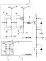
- FIG. 1 is a diagram of a gate drive circuit for an insulated gate power semiconductor device according to Embodiment 1 of the present invention.
- the power converter includes a plurality of insulated gate power semiconductor elements 1.
- each of the plurality of insulated gate power semiconductors is formed of an Nch MOSFET.
- the power converter converts DC power into AC power by the operation of the plurality of insulated gate power semiconductor elements 1.
- the power converter supplies the AC power to a motor (not shown).
- Each of the gate drive circuits 2 is provided corresponding to each of the insulated gate power semiconductor elements 1.
- the gate drive circuit 2 includes a resistor 3, an Nch MOSFET 4, a Pch MOSFET 5, a control circuit 6, and a power supply body 7.
- the resistor 3 is connected to the gate electrode of the insulated gate power semiconductor element 1.
- the Nch MOSFET 4 has a source electrode, a drain electrode, and a gate electrode.
- the source electrode of the Nch MOSFET 4 is connected to the gate electrode of the insulated gate power semiconductor element 1 through the resistor 3.
- the Pch MOSFET 5 has a source electrode, a drain electrode, and a gate electrode.
- the source electrode of the Pch MOSFET 5 is connected to the gate electrode of the insulated gate power semiconductor element 1 through the resistor 3.
- the control circuit 6 includes a positive side switching element 6a and a negative side switching element 6b.
- the positive side switching element 6a has an emitter electrode, a collector electrode, and a base electrode.
- the emitter electrode of the positive side switching element 6a is connected to the gate electrode of the Nch MOSFET 4 and the gate electrode of the Pch MOSFET 5.
- the emitter electrode of the positive side switching element 6 a becomes a control electrode of the control circuit 6.
- the collector electrode of the positive side switching element 6 a becomes the positive side electrode of the control circuit 6.
- the emitter electrode of negative side switching element 6 b is connected to the gate electrode of NchMOSFET 4 and the gate electrode of PchMOSFET 5.
- the emitter electrode of the negative side switching element 6 b becomes a control electrode of the control circuit 6.
- the collector electrode of the negative side switching element 6 b becomes the negative side electrode of the control circuit 6.
- the power supply body 7 includes a positive power supply body 8 and a negative power supply body 9.
- the positive power supply 8 includes a first positive power supply 8a and a second positive power supply 8b.
- the positive electrode of the first positive power supply 8a is connected to the drain electrode of the Nch MOSFET 4.
- the negative electrode of the first positive power supply 8 a is connected to the source electrode of the insulated gate power semiconductor element 1.
- the positive side electrode of the second positive side power supply 8b is connected to the collector electrode of the positive side switching element 6a.
- the negative electrode of the second positive power supply 8 b is connected to the source electrode of the insulated gate power semiconductor element 1.
- the positive electrode of the negative power source body 9 is connected to the source electrode of the insulated gate power semiconductor element 1.
- the negative electrode of the negative power supply body 9 is connected to the drain electrode of the Pch MOSFET 5 and the collector electrode of the negative switching element 6b.
- the negative power source body 9 applies a negative voltage of ⁇ 15 V to the drain electrode of the Pch MOSFET 5 and the collector electrode of the negative side switching element 6b.
- the first positive power supply 8 a applies a positive voltage of +15 V to the drain electrode of the Nch MOSFET 4.
- the second positive power supply 8b applies a positive voltage having an absolute value larger than the absolute value of the positive voltage applied by the first positive power supply 8a to the collector electrode of the positive switching element 6a.
- the difference between the absolute value of the positive voltage and the absolute value of the positive voltage applied by the first positive power supply 8a is set to a value larger than the value of the gate threshold voltage of the Nch MOSFET 4.
- the second positive power supply 8b applies a positive voltage of +20 V to the collector electrode of the positive switching element 6a.
- a negative voltage of ⁇ 15V is applied to the gate electrode of the PchMOSFET 5.
- the Pch MOSFET 5 is turned on.
- a negative voltage is applied to the gate electrode of the insulated gate power semiconductor element 1.
- the insulated gate power semiconductor element 1 is turned off.
- a positive voltage of + 20V is applied to the gate electrode of the Nch MOSFET 4.
- the Nch MOSFET 4 is turned on.
- a positive voltage is applied between the gate electrode and the source electrode of the Nch MOSFET 4.
- the positive voltage is +5 V obtained by subtracting +15 V applied to the drain electrode from +20 V applied to the gate electrode of the Nch MOSFET 4.
- the potential difference between the drain electrode and the source electrode of the Nch MOSFET 4 is sufficiently small.
- a positive voltage of +15 V is applied between the gate electrode and the source electrode of the insulated gate power semiconductor element 1.
- variations in the gate threshold voltage of the Nch MOSFET 4 are not affected.
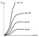
- FIG. 2 is a diagram for explaining the characteristics of the insulated gate power semiconductor device according to the first embodiment of the present invention.
- Vgs represents a voltage between the gate electrode and the source electrode of the insulated gate power semiconductor element 1.
- Vds represents a voltage between the drain electrode and the source electrode of the insulated gate power semiconductor element 1.
- Id represents the drain current of the insulated gate power semiconductor element 1.
- the power supply body 7 applies a positive voltage having an absolute value larger than the absolute value of the positive voltage applied to the drain electrode of the Nch MOSFET 4 to the positive electrode of the control circuit 6.
- the positive voltage By applying the positive voltage, the potential difference between the drain electrode and the source electrode of the Nch MOSFET 4 becomes sufficiently small.
- a large voltage can be stably applied to the gate electrode of the insulated gate power semiconductor element 1.
- the efficiency of the power converter is improved.
- size reduction and cost reduction of a power converter are realizable.
- the temperature rise value of a power converter becomes small by efficiency improvement of a power converter. For this reason, the lifetime improvement of a power converter is realizable.
- the positive power supply 8 includes a first positive power supply 8a and a second positive power supply 8b.
- the first positive power supply 8 a applies a positive voltage to the drain electrode of the Nch MOSFET 4.
- the second positive power supply 8 b applies a positive voltage having an absolute value larger than the absolute value of the positive voltage applied to the drain electrode of the Nch MOSFET 4 to the positive electrode of the control circuit 6. For this reason, the deterioration of the steady loss of the insulated gate type power semiconductor element 1 can be prevented only by using two different positive power supplies.
- FIG. FIG. 3 is a diagram of a gate drive circuit for an insulated gate power semiconductor device according to the second embodiment of the present invention.
- symbol is attached
- the power supply body 7 according to the first embodiment applies the same negative voltage to the drain electrode of the Pch MOSFET 5 and the negative electrode of the control circuit 6.
- the power supply body 7 according to the second embodiment applies a negative voltage having an absolute value larger than the absolute value of the negative voltage applied to the drain electrode of the Pch MOSFET 5 to the negative electrode of the control circuit 6.
- the negative power source body 9 includes a first negative power source 9a and a second negative power source 9b.
- the first negative power supply 9 a applies a negative voltage to the drain electrode of the Pch MOSFET 5.
- the second negative power source 9 b applies a negative voltage having an absolute value larger than the absolute value of the negative voltage applied to the drain electrode of the Pch MOSFET 5 to the negative electrode of the control circuit 6.
- the difference between the absolute value of the negative voltage and the absolute value of the negative voltage applied to the drain electrode of the Pch MOSFET 5 is set to a value larger than the gate threshold voltage value of the Pch MOSFET 5.
- the second negative power supply 9b applies a negative voltage of ⁇ 20 V to the collector electrode of the negative switching element 6b.
- the power supply 7 applies a negative voltage having an absolute value larger than the absolute value of the negative voltage applied to the drain electrode of the Pch MOSFET 5 to the negative electrode of the control circuit 6.
- the positive voltage By applying the positive voltage, the potential difference between the drain electrode and the source electrode of the Pch MOSFET 5 becomes sufficiently small. For this reason, the negative voltage applied to the gate electrode of the insulated gate type power semiconductor element 1 can be stabilized.
- the negative power source body 9 includes a first negative power source 9a and a second negative power source 9b.
- the first negative power supply 9 a applies a negative voltage to the drain electrode of the Pch MOSFET 5.
- the second negative power supply applies a negative voltage having an absolute value larger than the absolute value of the negative voltage applied to the drain electrode of the Pch MOSFET 5 to the negative electrode of the control circuit 6. For this reason, the negative voltage applied to the gate electrode of the insulated gate power semiconductor element 1 can be stabilized only by using two different negative power sources.
- FIG. 4 is a diagram of a gate drive circuit for an insulated gate power semiconductor device according to a third embodiment of the present invention.
- symbol is attached
- the gate drive circuit 2 according to the third embodiment is a circuit in which a positive side zener diode 10 and a negative side zener diode 11 are added to the gate drive circuit 2 according to the second embodiment.
- the positive side zener diode 10 is connected between the gate electrode and the source electrode of the Nch MOSFET 4.
- Negative side zener diode 11 is connected between the gate electrode and source electrode of PchMOSFET 5.
- the Nch MOSFET 4 When the insulated gate power semiconductor element 1 is turned on from off, the Nch MOSFET 4 is turned on from off. At this time, the time during which the voltage between the gate electrode and the source electrode of the insulated gate type power semiconductor element 1 changes from the negative voltage to the positive voltage is changed from the negative voltage to the positive voltage. It may be longer than the time to change.
- a large positive voltage can be applied between the gate electrode and the source electrode of the Nch MOSFET 4.
- the absolute value of the positive voltage is 30 (V), which is the sum of the positive voltage of the first positive power supply 8a and the negative voltage of the first negative power supply 9a.
- the absolute value of the positive voltage is larger than the absolute value of the maximum rated voltage between the gate electrode and the source electrode of the Nch MOSFET 4.
- Zener voltage needs to be selected to be smaller than the absolute value of the maximum rated voltage between the gate electrode and the source electrode of the Nch MOSFET 4.
- the PchMOSFET 5 When the insulated gate power semiconductor element 1 is turned off, the PchMOSFET 5 is turned on. At this time, the time during which the voltage between the gate electrode and the source electrode of the insulated gate power semiconductor element 1 changes from the positive voltage to the negative voltage is changed from the negative voltage to the positive voltage. It may be longer than the time to change.
- a large negative voltage can be applied between the gate electrode and the source electrode of the Pch MOSFET 5.
- the absolute value of the negative voltage is 30 (V), which is the sum of the positive voltage of the first positive power supply 8a and the negative voltage of the first negative power supply 9a.
- the absolute value of the negative voltage is larger than the absolute value of the maximum rated voltage between the gate electrode and the source electrode of the Pch MOSFET 5.
- the Zener voltage needs to be selected to be smaller than the absolute value of the maximum rated voltage between the gate electrode and the source electrode of the Pch MOSFET 5.
- the positive-side Zener diode 10 is connected between the gate electrode and the source electrode of the Nch MOSFET 4. For this reason, it is possible to prevent the Nch MOSFET 4 from being destroyed when the insulated gate power semiconductor element 1 is turned on from off.
- the negative side Zener diode 11 is connected between the gate electrode and the source electrode of the PchMOSFET 5. Therefore, it is possible to prevent the Pch MOSFET 5 from being destroyed when the insulated gate power semiconductor element 1 is turned from on to off.
- the gate drive circuit 2 may be applied to an insulated gate power semiconductor element of a power converter that converts AC power into DC power.
- the output electrode of the control circuit 6 may be connected to at least one of the gate electrode of the Nch MOSFET 4 and the gate electrode of the Pch MOSFET 5 via a resistor.
- the first resistor and the second resistor may be used instead of the resistor 3.
- a first resistor may be provided between the drain electrode of the Nch MOSFET 4 and the first positive power supply 8a. What is necessary is just to provide a 2nd resistance between the drain electrode of PchMOSFET5 and the negative side power supply body 9 or 9a.
- the gate electrode of the insulated gate power semiconductor element 1 is directly connected to at least one of the source electrode of the Nch MOSFET 4 and the source electrode of the Pch MOSFET 5 without the resistor 3. Also good.
- a semiconductor element different from the Nch MOSFET may be used as the insulated gate power semiconductor element 1.
- a semiconductor element formed by IGBT may be the insulated gate power semiconductor element 1.
- a semiconductor element formed of a wide band gap semiconductor may be used as the insulated gate power semiconductor element 1.
- the wide band gap semiconductor includes silicon carbide, a gallium nitride-based material, and diamond.
- the semiconductor element formed of a wide band gap semiconductor is the insulated gate power semiconductor element 1
- an improvement in the efficiency of the insulated gate power semiconductor element 1 itself can be expected.
- the magnitude of the steady loss based on the voltage applied to the gate electrode of the insulated gate power semiconductor element 1 greatly affects the loss of the power converter. For this reason, when the semiconductor element formed of a wide band gap semiconductor is the insulated gate power semiconductor element 1, the gate drive circuit 2 can exhibit a greater effect.
- the gate drive circuit for an insulated gate power semiconductor device can be used in a system that prevents deterioration of steady loss of the insulated gate power semiconductor device.
- 1 insulated gate type power semiconductor element 1 insulated gate type power semiconductor element, 2 gate drive circuit, 3 resistance, 4 Nch MOSFET, 5 Pch MOSFET, 6 control circuit, 6a positive side switching element, 6b negative side switching element, 7 power source body, 8 positive side power source body, 8a No. 1 positive power supply, 8b 2nd positive power supply, 9 negative power supply, 9a 1st negative power supply, 9b 2nd negative power supply, 10 positive zener diode, 11 negative zener diode
Landscapes
- Engineering & Computer Science (AREA)
- Power Engineering (AREA)
- Power Conversion In General (AREA)
- Electronic Switches (AREA)
- Metal-Oxide And Bipolar Metal-Oxide Semiconductor Integrated Circuits (AREA)
Abstract
Priority Applications (5)
| Application Number | Priority Date | Filing Date | Title |
|---|---|---|---|
| DE112014006783.0T DE112014006783T5 (de) | 2014-07-03 | 2014-07-03 | Gate-Treiberschaltung für Leistungshalbleiterelemente mit isoliertem Gate |
| JP2016530758A JP6299869B2 (ja) | 2014-07-03 | 2014-07-03 | 絶縁ゲート型パワー半導体素子のゲート駆動回路 |
| PCT/JP2014/067771 WO2016002041A1 (fr) | 2014-07-03 | 2014-07-03 | Circuit d'attaque de grille pour élément à semi-conducteur électrique du type à grille isolée |
| US15/320,658 US9966947B2 (en) | 2014-07-03 | 2014-07-03 | Gate driving circuit for insulated gate-type power semiconductor element |
| CN201480080132.8A CN106664085B (zh) | 2014-07-03 | 2014-07-03 | 绝缘栅型功率半导体元件的栅极驱动电路 |
Applications Claiming Priority (1)
| Application Number | Priority Date | Filing Date | Title |
|---|---|---|---|
| PCT/JP2014/067771 WO2016002041A1 (fr) | 2014-07-03 | 2014-07-03 | Circuit d'attaque de grille pour élément à semi-conducteur électrique du type à grille isolée |
Publications (1)
| Publication Number | Publication Date |
|---|---|
| WO2016002041A1 true WO2016002041A1 (fr) | 2016-01-07 |
Family
ID=55018640
Family Applications (1)
| Application Number | Title | Priority Date | Filing Date |
|---|---|---|---|
| PCT/JP2014/067771 Ceased WO2016002041A1 (fr) | 2014-07-03 | 2014-07-03 | Circuit d'attaque de grille pour élément à semi-conducteur électrique du type à grille isolée |
Country Status (5)
| Country | Link |
|---|---|
| US (1) | US9966947B2 (fr) |
| JP (1) | JP6299869B2 (fr) |
| CN (1) | CN106664085B (fr) |
| DE (1) | DE112014006783T5 (fr) |
| WO (1) | WO2016002041A1 (fr) |
Families Citing this family (1)
| Publication number | Priority date | Publication date | Assignee | Title |
|---|---|---|---|---|
| KR102447530B1 (ko) * | 2016-04-15 | 2022-09-26 | 엘지전자 주식회사 | 냉장고 |
Citations (2)
| Publication number | Priority date | Publication date | Assignee | Title |
|---|---|---|---|---|
| US20020163040A1 (en) * | 2001-05-02 | 2002-11-07 | International Rectifier Corp. | Power mosfet with integrated drivers in a common package |
| US20100237911A1 (en) * | 2007-10-05 | 2010-09-23 | Andreas Svensson | Drive Circuit For A Power Switch Component |
Family Cites Families (12)
| Publication number | Priority date | Publication date | Assignee | Title |
|---|---|---|---|---|
| JP2795027B2 (ja) | 1992-02-17 | 1998-09-10 | 三菱電機株式会社 | Igbtのゲート駆動回路 |
| JPH06244698A (ja) * | 1993-02-19 | 1994-09-02 | Pfu Ltd | ゲート・ドライブ回路 |
| US5399920A (en) * | 1993-11-09 | 1995-03-21 | Texas Instruments Incorporated | CMOS driver which uses a higher voltage to compensate for threshold loss of the pull-up NFET |
| DE19806311A1 (de) * | 1998-02-16 | 1999-08-26 | Siemens Ag | Vorrichtung zum Schalten induktiver Verbraucher |
| JP3636140B2 (ja) * | 2002-02-04 | 2005-04-06 | サンケン電気株式会社 | ゲート駆動回路 |
| JP2005108980A (ja) * | 2003-09-29 | 2005-04-21 | Rohm Co Ltd | 半導体装置 |
| US9184739B2 (en) * | 2011-06-09 | 2015-11-10 | Mitsubishi Electric Corporation | Gate drive circuit |
| TWI513190B (zh) * | 2011-07-22 | 2015-12-11 | Hon Hai Prec Ind Co Ltd | 使金氧半導體場效電晶體輸出線性電流的閘極驅動電路 |
| JP5545308B2 (ja) * | 2012-02-28 | 2014-07-09 | 株式会社豊田中央研究所 | 駆動回路 |
| JP5755197B2 (ja) * | 2012-07-27 | 2015-07-29 | 三菱電機株式会社 | 電力変換装置 |
| US8742803B2 (en) * | 2012-09-26 | 2014-06-03 | Broadcom Corporation | Output driver using low voltage transistors |
| CN103839510A (zh) * | 2014-03-26 | 2014-06-04 | 华映视讯(吴江)有限公司 | 栅极驱动电路 |
-
2014
- 2014-07-03 WO PCT/JP2014/067771 patent/WO2016002041A1/fr not_active Ceased
- 2014-07-03 US US15/320,658 patent/US9966947B2/en active Active
- 2014-07-03 CN CN201480080132.8A patent/CN106664085B/zh active Active
- 2014-07-03 JP JP2016530758A patent/JP6299869B2/ja active Active
- 2014-07-03 DE DE112014006783.0T patent/DE112014006783T5/de active Pending
Patent Citations (2)
| Publication number | Priority date | Publication date | Assignee | Title |
|---|---|---|---|---|
| US20020163040A1 (en) * | 2001-05-02 | 2002-11-07 | International Rectifier Corp. | Power mosfet with integrated drivers in a common package |
| US20100237911A1 (en) * | 2007-10-05 | 2010-09-23 | Andreas Svensson | Drive Circuit For A Power Switch Component |
Also Published As
| Publication number | Publication date |
|---|---|
| DE112014006783T5 (de) | 2017-03-30 |
| US9966947B2 (en) | 2018-05-08 |
| CN106664085A (zh) | 2017-05-10 |
| JPWO2016002041A1 (ja) | 2017-04-27 |
| CN106664085B (zh) | 2019-10-22 |
| US20170179950A1 (en) | 2017-06-22 |
| JP6299869B2 (ja) | 2018-03-28 |
Similar Documents
| Publication | Publication Date | Title |
|---|---|---|
| US8952730B2 (en) | Driver circuit | |
| CN104205638B (zh) | 共射共基电路 | |
| JP5263317B2 (ja) | 半導体スイッチング素子の駆動回路 | |
| US8710541B2 (en) | Bi-directional switch using series connected N-type MOS devices in parallel with series connected P-type MOS devices | |
| JP6626267B2 (ja) | 半導体装置 | |
| TWI543519B (zh) | 橋式整流電路 | |
| JP6065721B2 (ja) | 駆動回路、半導体集積回路、及び駆動回路の制御方法 | |
| JP2016059180A (ja) | スイッチング電源 | |
| JP6458552B2 (ja) | スイッチング方式の降圧型dc−dcコンバータ、及び電力変換回路 | |
| US9742388B2 (en) | Driver circuit | |
| JP6229604B2 (ja) | 半導体スイッチング素子の制御回路 | |
| JP2017168924A (ja) | 半導体装置 | |
| JP5837499B2 (ja) | インバータ | |
| JP2019165608A (ja) | 半導体装置 | |
| US9787303B2 (en) | Driver circuit and switch driving method | |
| WO2014128942A1 (fr) | Dispositif de commande d'élément semi-conducteur | |
| US20150236635A1 (en) | Inverter output circuit | |
| JP6299869B2 (ja) | 絶縁ゲート型パワー半導体素子のゲート駆動回路 | |
| JP2013243877A (ja) | ゲート駆動回路 | |
| WO2016157813A1 (fr) | Appareil de pilotage de charge | |
| JP6009932B2 (ja) | ゲート駆動回路 | |
| JP5802618B2 (ja) | ゲート駆動回路 | |
| JP6096681B2 (ja) | 三相インバータ回路及びドライバ回路 | |
| JP6265849B2 (ja) | 制御回路 | |
| JP2017175178A (ja) | ゲート駆動回路、半導体装置 |
Legal Events
| Date | Code | Title | Description |
|---|---|---|---|
| 121 | Ep: the epo has been informed by wipo that ep was designated in this application |
Ref document number: 14896290 Country of ref document: EP Kind code of ref document: A1 |
|
| ENP | Entry into the national phase |
Ref document number: 2016530758 Country of ref document: JP Kind code of ref document: A |
|
| WWE | Wipo information: entry into national phase |
Ref document number: 15320658 Country of ref document: US |
|
| WWE | Wipo information: entry into national phase |
Ref document number: 112014006783 Country of ref document: DE |
|
| REG | Reference to national code |
Ref country code: BR Ref legal event code: B01A Ref document number: 112016030911 Country of ref document: BR |
|
| 122 | Ep: pct application non-entry in european phase |
Ref document number: 14896290 Country of ref document: EP Kind code of ref document: A1 |
|
| ENP | Entry into the national phase |
Ref document number: 112016030911 Country of ref document: BR Kind code of ref document: A2 Effective date: 20161229 |