WO2016002801A1 - Structure semi-conductrice stratifiée et élément à semi-conducteur - Google Patents
Structure semi-conductrice stratifiée et élément à semi-conducteur Download PDFInfo
- Publication number
- WO2016002801A1 WO2016002801A1 PCT/JP2015/068881 JP2015068881W WO2016002801A1 WO 2016002801 A1 WO2016002801 A1 WO 2016002801A1 JP 2015068881 W JP2015068881 W JP 2015068881W WO 2016002801 A1 WO2016002801 A1 WO 2016002801A1
- Authority
- WO
- WIPO (PCT)
- Prior art keywords
- layer
- substrate
- nitride semiconductor
- semiconductor
- gan
- Prior art date
- Legal status (The legal status is an assumption and is not a legal conclusion. Google has not performed a legal analysis and makes no representation as to the accuracy of the status listed.)
- Ceased
Links
Images













Classifications
-
- H—ELECTRICITY
- H10—SEMICONDUCTOR DEVICES; ELECTRIC SOLID-STATE DEVICES NOT OTHERWISE PROVIDED FOR
- H10D—INORGANIC ELECTRIC SEMICONDUCTOR DEVICES
- H10D10/00—Bipolar junction transistors [BJT]
- H10D10/80—Heterojunction BJTs
-
- H—ELECTRICITY
- H10—SEMICONDUCTOR DEVICES; ELECTRIC SOLID-STATE DEVICES NOT OTHERWISE PROVIDED FOR
- H10D—INORGANIC ELECTRIC SEMICONDUCTOR DEVICES
- H10D30/00—Field-effect transistors [FET]
- H10D30/60—Insulated-gate field-effect transistors [IGFET]
-
- H—ELECTRICITY
- H10—SEMICONDUCTOR DEVICES; ELECTRIC SOLID-STATE DEVICES NOT OTHERWISE PROVIDED FOR
- H10D—INORGANIC ELECTRIC SEMICONDUCTOR DEVICES
- H10D30/00—Field-effect transistors [FET]
- H10D30/80—FETs having rectifying junction gate electrodes
- H10D30/83—FETs having PN junction gate electrodes
-
- H—ELECTRICITY
- H10—SEMICONDUCTOR DEVICES; ELECTRIC SOLID-STATE DEVICES NOT OTHERWISE PROVIDED FOR
- H10D—INORGANIC ELECTRIC SEMICONDUCTOR DEVICES
- H10D30/00—Field-effect transistors [FET]
- H10D30/80—FETs having rectifying junction gate electrodes
- H10D30/87—FETs having Schottky gate electrodes, e.g. metal-semiconductor FETs [MESFET]
-
- H—ELECTRICITY
- H10—SEMICONDUCTOR DEVICES; ELECTRIC SOLID-STATE DEVICES NOT OTHERWISE PROVIDED FOR
- H10D—INORGANIC ELECTRIC SEMICONDUCTOR DEVICES
- H10D64/00—Electrodes of devices having potential barriers
- H10D64/01—Manufacture or treatment
- H10D64/011—Manufacture or treatment of electrodes ohmically coupled to a semiconductor
-
- H—ELECTRICITY
- H10—SEMICONDUCTOR DEVICES; ELECTRIC SOLID-STATE DEVICES NOT OTHERWISE PROVIDED FOR
- H10D—INORGANIC ELECTRIC SEMICONDUCTOR DEVICES
- H10D64/00—Electrodes of devices having potential barriers
- H10D64/20—Electrodes characterised by their shapes, relative sizes or dispositions
- H10D64/27—Electrodes not carrying the current to be rectified, amplified, oscillated or switched, e.g. gates
-
- H—ELECTRICITY
- H10—SEMICONDUCTOR DEVICES; ELECTRIC SOLID-STATE DEVICES NOT OTHERWISE PROVIDED FOR
- H10D—INORGANIC ELECTRIC SEMICONDUCTOR DEVICES
- H10D64/00—Electrodes of devices having potential barriers
- H10D64/60—Electrodes characterised by their materials
- H10D64/64—Electrodes comprising a Schottky barrier to a semiconductor
-
- H—ELECTRICITY
- H10—SEMICONDUCTOR DEVICES; ELECTRIC SOLID-STATE DEVICES NOT OTHERWISE PROVIDED FOR
- H10D—INORGANIC ELECTRIC SEMICONDUCTOR DEVICES
- H10D64/00—Electrodes of devices having potential barriers
- H10D64/60—Electrodes characterised by their materials
- H10D64/66—Electrodes having a conductor capacitively coupled to a semiconductor by an insulator, e.g. MIS electrodes
-
- H—ELECTRICITY
- H10—SEMICONDUCTOR DEVICES; ELECTRIC SOLID-STATE DEVICES NOT OTHERWISE PROVIDED FOR
- H10D—INORGANIC ELECTRIC SEMICONDUCTOR DEVICES
- H10D8/00—Diodes
- H10D8/60—Schottky-barrier diodes
-
- H—ELECTRICITY
- H10—SEMICONDUCTOR DEVICES; ELECTRIC SOLID-STATE DEVICES NOT OTHERWISE PROVIDED FOR
- H10H—INORGANIC LIGHT-EMITTING SEMICONDUCTOR DEVICES HAVING POTENTIAL BARRIERS
- H10H20/00—Individual inorganic light-emitting semiconductor devices having potential barriers, e.g. light-emitting diodes [LED]
- H10H20/80—Constructional details
- H10H20/81—Bodies
- H10H20/815—Bodies having stress relaxation structures, e.g. buffer layers
-
- H—ELECTRICITY
- H10—SEMICONDUCTOR DEVICES; ELECTRIC SOLID-STATE DEVICES NOT OTHERWISE PROVIDED FOR
- H10H—INORGANIC LIGHT-EMITTING SEMICONDUCTOR DEVICES HAVING POTENTIAL BARRIERS
- H10H20/00—Individual inorganic light-emitting semiconductor devices having potential barriers, e.g. light-emitting diodes [LED]
- H10H20/80—Constructional details
- H10H20/81—Bodies
- H10H20/822—Materials of the light-emitting regions
- H10H20/824—Materials of the light-emitting regions comprising only Group III-V materials, e.g. GaP
- H10H20/825—Materials of the light-emitting regions comprising only Group III-V materials, e.g. GaP containing nitrogen, e.g. GaN
Definitions
- the present invention relates to a semiconductor multilayer structure and a semiconductor element.
- Patent Document 1 As a conventional light-emitting element, one formed by growing a crystal film on a surface of a translucent substrate on which a concavo-convex pattern is formed is known (for example, see Patent Document 1).
- Patent Document 1 a GaN-based semiconductor layer is grown on the surface of the sapphire substrate on which the concavo-convex pattern is formed.
- the concavo-convex pattern of the sapphire substrate of Patent Document 1 is emitted from the light emitting layer in the GaN-based semiconductor layer due to the difference in refractive index between the sapphire substrate and the GaN-based semiconductor layer at the interface between the sapphire substrate and the GaN-based semiconductor layer. It has a function of suppressing reflection of emitted light. By suppressing such reflection, absorption of reflected light by the light emitting layer and attenuation due to multiple reflection of reflected light can be reduced, and the light extraction efficiency of the light emitting element can be improved.
- the GaN-based semiconductor layer grows also from the side wall of the processed portion.
- a crystal having a c-axis in the vertical direction of the substrate and a crystal having a c-axis other than the vertical direction are mixed, and the GaN-based semiconductor layer becomes polycrystalline.
- the quality of the nitride semiconductor layer is remarkably deteriorated (see, for example, Patent Document 2).
- the present invention has been made in view of such circumstances, and an object of the present invention is to provide a semiconductor laminated structure having a nitride semiconductor layer having high quality on the gallium oxide substrate and high uniformity in the plane. And a semiconductor element including the semiconductor multilayer structure.
- One embodiment of the present invention provides a semiconductor stacked structure according to [1] to [5] in order to achieve the above object.
- the Ga 2 O 3 is formed so as to contact with the upper surface part on the substrate, the dielectric difference in refractive index between the Ga 2 O 3 substrate is 0.15 or less
- a buffer layer made of a GaN crystal so as to be in contact with the remaining upper surface of the Ga 2 O 3 substrate that is not covered with the dielectric layer, and the buffer layer on the Ga 2 O 3 substrate.
- another aspect of the present invention provides the semiconductor device according to [6].
- a semiconductor device comprising the semiconductor multilayer structure according to any one of [1] to [5] above.
- a nitride semiconductor layer having high quality and high in-plane uniformity that can comprehensively improve device characteristics determined by reliability, leakage current, temperature characteristics, light emission efficiency, and the like. It is possible to provide a semiconductor stacked structure having the semiconductor stack and a semiconductor element including the semiconductor stacked structure.
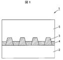
- FIG. 1 is a vertical sectional view of a semiconductor multilayer structure (first embodiment).
- Figure 2 is a conceptual diagram showing the orientation relationship between the ⁇ -Ga 2 O 3 and the unit cell of the crystal, ⁇ -Ga 2 O 3 principal surface of the substrate (the first embodiment).
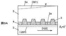
- FIG. 3A is a schematic diagram showing the relationship between the offset angle ⁇ s of the main surface of the Ga 2 O 3 substrate and the inclination angle ⁇ of the main surface of the nitride semiconductor layer (first embodiment).
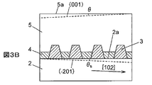
- FIG. 3B is a schematic diagram showing the relationship between the offset angle ⁇ s of the main surface of the Ga 2 O 3 substrate and the inclination angle ⁇ of the main surface of the nitride semiconductor layer (first embodiment).
- FIG. 3A is a schematic diagram showing the relationship between the offset angle ⁇ s of the main surface of the Ga 2 O 3 substrate and the inclination angle ⁇ of the main surface of the nitride semiconductor layer (first embodiment).
- FIG. 3B is a schematic diagram showing the
- FIG. 3C is a schematic diagram illustrating a relationship between an offset angle ⁇ s of the main surface of the Ga 2 O 3 substrate and an inclination angle ⁇ of the main surface of the nitride semiconductor layer (first embodiment).
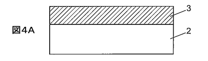
- FIG. 4A is a vertical cross-sectional view illustrating a manufacturing process of a semiconductor stacked structure (first embodiment).
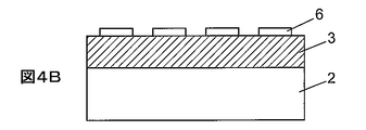
- FIG. 4B is a vertical cross-sectional view illustrating the manufacturing process of the semiconductor stacked structure (first embodiment).
- FIG. 4C is a vertical cross-sectional view illustrating the manufacturing process of the semiconductor stacked structure (first embodiment).
- FIG. 4D is a vertical cross-sectional view illustrating the manufacturing process of the semiconductor stacked structure (first embodiment).
- FIG. 4E is a vertical cross-sectional view illustrating the manufacturing process of the semiconductor stacked structure (first embodiment).
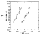
- FIG. 5A is a graph showing variation in crystal quality of a nitride semiconductor layer for each semiconductor stacked structure (first embodiment).
- FIG. 5B is a graph showing variation in crystal quality of the nitride semiconductor layer for each semiconductor stacked structure (first embodiment).
- FIG. 6 is a graph showing variations in dislocation density for each semiconductor stacked structure (first embodiment).
- FIG. 7 is a vertical sectional view of a semiconductor laminated structure in which electrodes for measuring current-voltage characteristics are connected (first embodiment).
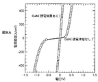
- FIG. 8A is a graph showing the current density-voltage characteristic in the vertical direction of the semiconductor multilayer structure (first embodiment).
- FIG. 8B is a graph showing the current density-voltage characteristics in the vertical direction of the semiconductor stacked structure (first embodiment).
- FIG. 9 is a graph showing an example of the relationship between the material of the dielectric layer and the light extraction efficiency of the light emitting element obtained by optical simulation (first embodiment).
- FIG. 10A is a graph showing variation in crystal quality of a nitride semiconductor layer for each semiconductor stacked structure (first embodiment).
- FIG. 10B is a graph showing variation in crystal quality of the nitride semiconductor layer for each semiconductor stacked structure (first embodiment).
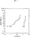
- FIG. 11 is a graph showing variation in ⁇ for each semiconductor stacked structure (first embodiment).
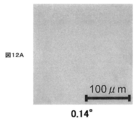
- FIG. 12A is a photograph showing the state of the main surface of the nitride semiconductor layer when the inclination angle ⁇ of the main surface of the nitride semiconductor layer is 0.14 ° (first embodiment).
- FIG. 12B is a photograph showing the state of the main surface of the nitride semiconductor layer when the inclination angle ⁇ of the main surface of the nitride semiconductor layer is 0.25 ° (first embodiment).
- FIG. 12C is a photograph showing the state of the main surface of the nitride semiconductor layer when the inclination angle ⁇ of the main surface of the nitride semiconductor layer is 0.45 ° (first embodiment).
- FIG. 12A is a photograph showing the state of the main surface of the nitride semiconductor layer when the inclination angle ⁇ of the main surface of the nitride semiconductor layer is 0.14 ° (first embodiment).
- FIG. 12B is a photograph showing the state of the main surface of the nitride semiconductor layer when the inclination angle
- FIG. 12D is a photograph showing the state of the main surface of the nitride semiconductor layer when the inclination angle ⁇ of the main surface of the nitride semiconductor layer is 0.63 ° (first embodiment).
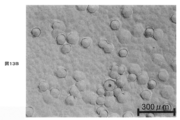
- FIG. 13A is a photograph showing the state of the main surface of a nitride semiconductor layer when a GaN buffer layer is used (first embodiment).
- FIG. 13B is a photograph showing the state of the main surface of the nitride semiconductor layer when an AlN buffer layer is used (first embodiment).
- FIG. 14 is a vertical sectional view of a vertical LED (second embodiment).
- FIG. 15 is a vertical sectional view of a vertical FET (third embodiment).
- FIG. 16 is a vertical sectional view of a vertical FET (fourth embodiment).
- FIG. 17 is a vertical sectional view of a vertical FET (fifth embodiment).
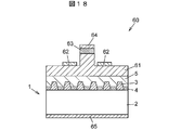
- FIG. 18 is a vertical sectional view of a vertical FET (sixth embodiment).
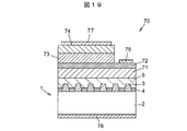
- FIG. 19 is a vertical sectional view of an HBT (seventh embodiment).
- FIG. 20 is a vertical sectional view of an SBD (eighth embodiment).
- the Ga 2 O 3 substrate 2 is made of ⁇ -Ga 2 O 3 single crystal.
- the upper surface of the Ga 2 O 3 substrate 2 is a flat surface without unevenness, and can serve as a foundation for the growth of high-quality nitride semiconductor crystals (101), ( ⁇ 201), (310), (3 A plane having a plane orientation of ⁇ 10), (100), etc.
- the refractive index of the Ga 2 O 3 substrate 2 is approximately 1.9.
- FIG. 2 is a conceptual diagram showing the orientation relationship between the unit cell of ⁇ -Ga 2 O 3 crystal and the main surface 2 a of the ⁇ -Ga 2 O 3 substrate 2.
- ⁇ s represents an offset angle in the [102] direction from the ( ⁇ 201) plane.
- the offset angle from the ( ⁇ 201) plane in the [010] direction is 0 °.
- a unit cell 2b in FIG. 2 is a unit cell of ⁇ -Ga 2 O 3 crystal.
- a 0 , b 0 , and c 0 represent axis lengths in the [100] direction, [010] direction, and [001] direction, respectively.
- the main surface 2a of the Ga 2 O 3 substrate 2 is a surface inclined with an offset angle ⁇ s in the [102] direction with respect to the ( ⁇ 201) plane, ie, the normal vector is based on the normal vector of the ( ⁇ 201) plane.
- the surface is inclined at an offset angle ⁇ s in the [102] direction.
- the offset angle ⁇ s is preferably ⁇ 0.4 ° or more and 0.2 ° or less, and more preferably ⁇ 0.2 ° or more and 0.0 ° or less.
- the dielectric layer 3 is made of, for example, a SiN layer containing SiN as a main component, and has a refractive index difference of 0.15 or less with respect to the Ga 2 O 3 substrate 2.
- the refractive index of the Ga 2 O 3 substrate 2 is 1.9, for example, the refractive index of the dielectric layer 3 is 1.75 or more and 2.05 or less.
- the pattern shape of the dielectric layer 3 is, for example, a mesa pattern, a recess pattern, a line and space pattern, or the like.
- Refractive index of the dielectric layer 3 is closer to the refractive index of the Ga 2 O 3 substrate 2, to suppress the total reflection at the interface of Ga 2 O 3 substrate 2 and the dielectric layer 3, the efficiency of the light from the light-emitting layer Can be taken out.
- the dielectric layer 3 is a SiN layer, elements other than Si and N such as O may be included for adjusting the refractive index.
- the refractive index of the dielectric layer 3 is adjusted by controlling the formation conditions such as the film formation temperature of the dielectric layer 3, and the difference between the refractive index of the dielectric layer 3 and the refractive index of the Ga 2 O 3 substrate 2 is adjusted. Can be made smaller.
- the GaN buffer layer 4 is made of a GaN crystal and may contain a conductivity type impurity such as Si.
- the nitride semiconductor layer 5 Crystal quality can be increased.
- the nitride semiconductor layer 5 may have a multilayer structure in which a plurality of layers made of different nitride semiconductor crystals are stacked.
- the light emitting layer and the clad layer sandwiching the light emitting layer can be constituted by the nitride semiconductor layer 5.
- the Ga 2 O 3 substrate 2 and the nitride semiconductor layer 5 may include a conductive impurity such as Si or Sn.
- FIG. 3A to 3C are schematic diagrams showing the relationship between the offset angle ⁇ s of the main surface 2a of the Ga 2 O 3 substrate 2 and the inclination angle ⁇ of the main surface 5a of the nitride semiconductor layer 5.
- FIG. 3A to 3C are planes parallel to the [102] direction, which are orthogonal to the ( ⁇ 201) plane of the Ga 2 O 3 substrate 2.
- the main surface 5a of the nitride semiconductor layer 5 has a predetermined inclination angle ⁇ . Tilted from the (001) plane.
- the inclination angle ⁇ of the main surface 5a of the nitride semiconductor layer 5 is made closer to 0 ° by providing the main surface 2a of the Ga 2 O 3 substrate 2 with an appropriate offset angle ⁇ s. Can do. Thereby, the surface roughness of main surface 5a of nitride semiconductor layer 5 can be effectively reduced.
- the inclination angle ⁇ of the main surface 5a of the nitride semiconductor layer 5 is set to 0.
- the offset angle ⁇ s of the main surface 2a of the Ga 2 O 3 substrate 2 is ⁇ 0.2 ° or more and 0.0 ° or less.
- the inclination angle ⁇ of the main surface 5a of the nitride semiconductor layer 5 can be within a numerical range of ⁇ 0.2 ° to 0.2 ° which is closer to 0 °.
- 4A to 4E are vertical cross-sectional views showing the manufacturing process of the semiconductor multilayer structure according to the first embodiment.
- organic cleaning and SPM (Sulfuric acid / hydrogen peroxide mixture) cleaning are performed on the Ga 2 O 3 substrate 2 subjected to CMP (Chemical Mechanical Polishing).
- the Ga 2 O 3 substrate 2 is transferred into the chamber of the plasma CVD apparatus.
- a film-like dielectric layer 3 is formed on the Ga 2 O 3 substrate 2.
- This film-like dielectric layer 3 is made of SiH 4 as a raw material of Si, NH 3 gas as a raw material of N, and N 2 gas as an atmospheric gas while maintaining the temperature in the chamber at 300 to 350 ° C. Is supplied into the chamber, and SiN is deposited on the Ga 2 O 3 substrate 2.
- the dielectric layer 3 is a substantially uniform film having a thickness of about 1 ⁇ m.
- the raw materials for each element are not limited to the above.
- a resist pattern 6 is formed on the dielectric layer 3.
- the pattern shape of the resist pattern 6 is, for example, a triangular lattice pattern with a dot diameter of 2 ⁇ m and a pitch of 4 ⁇ m.
- the resist pattern 6 is formed by, for example, photolithography.
- the dielectric layer 3 is etched with BHF (buffered hydrofluoric acid) using the resist pattern 6 as a mask, and the pattern of the resist pattern 6 is transferred to the dielectric layer 3.
- BHF buffered hydrofluoric acid
- the remaining resist pattern 6 is removed.
- the surface of the structure composed of the Ga 2 O 3 substrate 2 and the dielectric layer 3 is cleaned by organic cleaning and SPM cleaning, and transported to the MOCVD apparatus.
- GaN buffer layer 4 is formed by maintaining NH 3 as a raw material for N, trimethyl gallium (TMG) as a raw material for Ga, and maintaining the substrate surface temperature at around 500 ° C.
- TMG trimethyl gallium
- NH 3 gas as a raw material for N trimethylgallium (TMG) gas as a raw material for Ga
- trimethylaluminum (TMA) gas as a raw material for Al trimethylindium (TMI) gas as a raw material for In are contained in the chamber.
- the Al x Ga y In z N crystal which is a nitride semiconductor crystal, is selectively grown on the Ga 2 O 3 substrate 2 to form the nitride semiconductor layer 5. Thereby, the semiconductor multilayer structure 1 is obtained.
- the nitride semiconductor crystal constituting the nitride semiconductor layer 5 grows from a region not covered by the dielectric layer 3 on the upper surface of the Ga 2 O 3 substrate 2 and does not grow from the dielectric layer 3.
- the nitride semiconductor crystal grows selectively, and then grows in the lateral direction to cover the dielectric layer 3.
- the dislocation density in the nitride semiconductor layer 5 is reduced, and the crystal quality is improved.
- Such a crystal growth method using selective growth is called ELO (Epitaxial Lateral Overgrowth).
- (Crystal quality) 5A and 5B are graphs showing variations in crystal quality of the nitride semiconductor layer 5 for each semiconductor stacked structure 1.
- 5A shows the cumulative relative power distribution of the half width of the X-ray rocking curve in the (002) plane diffraction of the nitride semiconductor layer 5
- FIG. 5B shows the X-ray rocking curve in the (101) plane diffraction of the nitride semiconductor layer 5.
- the marks ⁇ plotted in FIGS. 5A and 5B represent the cumulative relative frequency distribution of the full width at half maximum of the X-ray rocking curve in the semiconductor multilayer structure 1 using the GaN buffer layer 4, and the marks ⁇ used the AlN buffer layer.
- the cumulative relative frequency distribution of the half value width of the X-ray rocking curve in a semiconductor lamination structure is expressed.
- 5A and 5B show that, when the GaN buffer layer 4 is used, the variation in the crystal quality of the nitride semiconductor layer 5 for each semiconductor stacked structure 1 does not change much as compared with the case where the AlN buffer layer is used. It shows that the crystal quality of the physical semiconductor layer 5 is improved.
- the half width was 223 to 269 arcsec in (002) plane diffraction and 225 to 264 arcsec in (101) plane diffraction.
- FIG. 6 is a graph showing variation in dislocation density for each semiconductor stacked structure.
- the mark ⁇ plotted in FIG. 6 represents the cumulative relative frequency distribution of the dislocation density of the X-ray rocking curve in the semiconductor multilayer structure 1 using the GaN buffer layer 4, and the mark ⁇ represents the semiconductor multilayer using the AlN buffer layer. It represents the cumulative relative frequency distribution of the dislocation density of the structure.
- the dislocation density was evaluated by using cathodoluminescence and counting the density of dark spots.
- the dislocation density evaluation results can also be obtained by counting the density of etch pits obtained by TEM observation or chemical etching using KOH, NaOH, or the like.
- FIG. 6 shows that in both the measurement results for the GaN buffer layer 4 and the AlN buffer layer, the crystal quality of the nitride semiconductor layer 5 varies from one semiconductor stack structure 1 to another and the dislocation density is almost the same. This value is comparable to that on the sapphire substrate, indicating that the crystal quality of the nitride semiconductor layer 5 is high.
- the dislocation density when using the GaN buffer layer 4 was 1.52 ⁇ 10 8 to 2.14 ⁇ 10 8 / cm 2 .
- FIG. 7 shows a state in which electrodes are connected to the Ga 2 O 3 substrate 2 and the nitride semiconductor layer 5 of the semiconductor multilayer structure 1.
- FIG. 8A and 8B are graphs showing the current density-voltage characteristics in the vertical direction of the semiconductor multilayer structure 1.
- the horizontal axis represents voltage (V)
- the vertical axis represents current density (A / cm 2 ).
- FIG. 8A shows the current density-voltage characteristic when the GaN buffer layer 4 is used
- FIG. 8B shows the current density-voltage characteristic when the AlN buffer layer is used.
- the plotted mark ⁇ represents the current density-voltage characteristic in the vertical direction of the semiconductor multilayer structure 1 without the dielectric layer 3, and the mark ⁇ represents the semiconductor multilayer structure with the dielectric layer. Represents the current density-voltage characteristics in the vertical direction.
- the dielectric layer 3 is a SiN layer, it has been confirmed that the current density-voltage characteristics in the vertical direction (vertical direction) of the semiconductor multilayer structure 1 can be obtained particularly excellent.
- the semiconductor laminated structure having the dielectric layer 3 that is the SiN layer is used to cause a specific current to flow more than the semiconductor laminated structure that does not have the dielectric layer that is the SiN layer.
- the required voltage is small. This result indicates that the drive voltage can be reduced by providing the dielectric layer 3 which is a SiN layer.
- FIG. 9 is a graph showing an example of the relationship between the material of the dielectric layer 3 and the light extraction efficiency of the light emitting element obtained by optical simulation.
- the Ga 2 O 3 substrate 2 has a refractive index of 1.9
- the dielectric layer 3 is composed of a mesa pattern having a diameter of 3 ⁇ m, a pitch of 6 ⁇ m, and a height of 1 ⁇ m, and light emitted from the light emitting layer.
- the light extraction efficiency in FIG. 9 is standardized on the basis of the light extraction efficiency in the case where unevenness of the same shape is formed on the surface of the Ga 2 O 3 substrate 2 instead of the dielectric layer in the light emitting element.
- this standard light extraction efficiency is that an n-type cladding layer, a light-emitting layer, a p-type cladding layer, and a contact layer with good crystal quality are formed on the Ga 2 O 3 substrate 2 having irregularities formed on the surface. This is the theoretical value when assumed.
- FIG. 9 shows that when the SiN layer that satisfies the refractive index condition of the dielectric layer is used as the dielectric layer 3, the light extraction efficiency is the highest.
- the light extraction efficiency is about 98.5% or more of the reference value.
- FIG. 10A and 10B are graphs showing an in-plane distribution of the difference ⁇ between the offset angle ⁇ s of the main surface of the Ga 2 O 3 substrate 2 and the inclination angle ⁇ of the main surface of the nitride semiconductor layer 5. It is.
- FIG. 10A shows the distribution of ⁇ when the GaN buffer layer 4 is used
- FIG. 10B shows the distribution of ⁇ when the AlN buffer layer is used.
- the horizontal axis in FIGS. 10A and 10B represents the position in the X direction or Y direction in the plane of the semiconductor multilayer structure 1.
- the mark ⁇ plotted in FIGS. 10A and 10B represents a measured value on a line parallel to the [010] direction of the Ga 2 O 3 substrate 2 through the center in the plane of the semiconductor multilayer structure 1.
- the mark ⁇ represents a measured value on a line parallel to the [102] direction of the Ga 2 O 3 substrate 2 through the center in the plane of the semiconductor multilayer structure 1.
- the variation in ⁇ in the plane of the semiconductor multilayer structure 1 is smaller in both the [010] direction and the [102] direction when the AlN buffer layer is used.
- the difference between the maximum value and the minimum value of ⁇ in the plane was 0.15 ° in the [010] direction and 0.07 ° in the [102] direction.
- FIG. 11 is a graph showing variation in ⁇ in the [102] direction of the Ga 2 O 3 substrate 2 for each semiconductor multilayer structure 1.
- the vertical axis represents the cumulative relative frequency distribution of ⁇ .
- 11 represents the cumulative relative power distribution of ⁇ in the semiconductor multilayer structure 1 using the GaN buffer layer 4, and the mark ⁇ represents the cumulative ⁇ in the semiconductor multilayer structure using the AlN buffer layer. Represents a relative frequency distribution. Note that these values of ⁇ are measured at the center position in the plane.
- FIG. 11 shows that when the GaN buffer layer 4 is used, the variation in ⁇ for each semiconductor multilayer structure 1 is smaller than when the AlN buffer layer is used.
- the difference between the maximum value and the minimum value of ⁇ between the semiconductor stacked structures when the GaN buffer layer 4 was used was 0.12 °.
- the inclination angle ⁇ of the main surface of the nitride semiconductor layer 5 in the [102] direction of the Ga 2 O 3 substrate 2 is 0.14 °, 0.25 °, 0.45 °, 0.63 °. 6 is a photograph showing the state of the main surface of nitride semiconductor layer 5 when.
- step bunching appearing on the main surface of the nitride semiconductor layer 5 increases as the tilt angle ⁇ increases.
- Step bunching is hardly confirmed on the main surface of the nitride semiconductor layer 5 shown in FIGS. 12A and 12B, but step bunching is clearly confirmed on the main surface of the nitride semiconductor layer 5 shown in FIGS. 12C and 12D. it can.
- the step bunching can be clearly confirmed when the inclination angle ⁇ is larger than approximately 0.4 ° (smaller than ⁇ 0.4 °). Further, when the inclination angle ⁇ is approximately ⁇ 0.2 ° or more and 0.2 ° or less, it is presumed that the step bunching becomes smaller and the smooth surface is obtained as the observation with the optical microscope becomes difficult.
- FIG. 13A is a photograph showing the state of the main surface of the nitride semiconductor layer 5 when the GaN buffer layer 4 is used
- FIG. 13B is a photograph of the main surface of the nitride semiconductor layer when the AlN buffer layer is used. It is a photograph showing the state.
- FIGS. 13A and 13B when the GaN buffer layer 4 is used, the hillock-like convex portions observed on the main surface of the nitride semiconductor layer 5 are greatly reduced as compared with the case where the AlN buffer layer is used. Is shown.
- the hillock density of the main surface of the nitride semiconductor layer 5 is less than 1 per 1 cm 2 when the GaN buffer layer 4 is used, and 10 2 to 10 3 per 1 cm 2 when the AlN buffer layer is used. It was a piece.
- the generation of hillocks is hardly affected by the inclination angle ⁇ of the main surface of the nitride semiconductor layer 5, but the surface flatness is improved more effectively by reducing the hillock density using the GaN buffer layer 4. can do.
- the semiconductor multilayer structure 1 according to the first embodiment can be used for manufacturing various semiconductor elements. Below, vertical LED is demonstrated as an example of the semiconductor element.
- FIG. 14 is a vertical sectional view of the vertical LED 10 according to the second embodiment.
- the vertical LED 10 includes a Ga 2 O 3 substrate 2, a dielectric layer 3 and a GaN buffer layer 4 on the Ga 2 O 3 substrate 2, an n-type cladding layer 14 on the GaN buffer layer 4, and an n-type cladding layer 14.
- the upper light emitting layer 15, the p-type cladding layer 16 on the light-emitting layer 15, the contact layer 17 on the p-type cladding layer 16, the p-type electrode 18 on the contact layer 17, and the GaN of the Ga 2 O 3 substrate 2 It has an n-type electrode 19 on the surface opposite to the buffer layer 4.
- the side surface of the laminate composed of the dielectric layer 3, the GaN buffer layer 4, the n-type cladding layer 14, the light emitting layer 15, the p-type cladding layer 16, and the contact layer 17 is covered with the insulating film 20.
- the n-type cladding layer 14 corresponds to the nitride semiconductor layer 5 constituting the semiconductor multilayer structure 1 of the first embodiment.
- the thicknesses of the Ga 2 O 3 substrate 2, the dielectric layer 3, the GaN buffer layer 4, and the n-type cladding layer 14 are, for example, 400 ⁇ m, 1 ⁇ m, 48 nm, and 5 ⁇ m.
- the light emitting layer 15 is composed of, for example, a three-layered multiple quantum well structure and a GaN crystal film having a thickness of 10 nm thereon.
- Each multiple quantum well structure is composed of a GaN crystal film having a thickness of 6 nm and an InGaN crystal film having a thickness of 2 nm.
- the light emitting layer 15 is formed by epitaxially growing each crystal film on the n-type cladding layer 14 at a growth temperature of 700 to 800 ° C., for example.
- the p-type cladding layer 16 is, for example, a GaN crystal film having a thickness of 100 nm and containing Mg having a concentration of 5.0 ⁇ 10 19 / cm 3 .
- the p-type cladding layer 16 is formed, for example, by epitaxially growing a GaN crystal containing Mg on the light emitting layer 15 at a growth temperature of 900 to 1050 ° C.
- the contact layer 17 is, for example, a GaN crystal film having a thickness of 10 nm and containing Mg having a concentration of 1.5 ⁇ 10 20 / cm 3 .
- the contact layer 17 is formed, for example, by epitaxially growing a GaN crystal containing Mg on the p-type cladding layer 16 at a growth temperature of 900 to 1050 ° C.
- the n-type cladding layer 14, the light emitting layer 15, the p-type cladding layer 16, and the contact layer 17 TMG (trimethylgallium) gas as the Ga material, TMI (trimethylindium) gas as the In material, MtSiH 3 (monomethylsilane) gas can be used as the Si material, Cp 2 Mg (biscyclopentadienylmagnesium) gas can be used as the Mg material, and NH 3 (ammonia) gas can be used as the N material.
- TMG trimethylgallium
- TMI trimethylindium
- MtSiH 3 (monomethylsilane) gas can be used as the Si material
- Cp 2 Mg (biscyclopentadienylmagnesium) gas can be used as the Mg material
- NH 3 (ammonia) gas can be used as the N material.
- the insulating film 20 is made of an insulating material made of SiO 2 or the like, and is formed, for example, by sputtering.
- the p-type electrode 18 and the n-type electrode 19 are electrodes that are in ohmic contact with the contact layer 17 and the Ga 2 O 3 substrate 2, respectively, and are formed by, for example, a vapor deposition apparatus.
- the vertical LED 10 includes a dielectric layer 3, a GaN buffer layer 4, an n-type cladding layer 14, a light-emitting layer 15, a p-type cladding layer 16, a contact layer 17, and a p-type electrode on a Ga 2 O 3 substrate 2 in a wafer state. After the 18 and n-type electrodes 19 are formed, they are obtained by dicing them into, for example, a 300 ⁇ m square chip size.
- the vertical LED 10 is, for example, an LED chip that extracts light from the Ga 2 O 3 substrate 2 side, and is mounted on a can-type stem using Ag paste.
- the n-type cladding layer 14 of the vertical LED 10 is formed on the Ga 2 O 3 substrate 2 whose main surface is a surface inclined at a special offset angle, the surface roughness is small and the crystal quality is excellent. .
- the light emitting layer 15, the p-type cladding layer 16, and the contact layer 17 formed by epitaxial crystal growth on the n-type cladding layer 14 having excellent crystal quality also have excellent crystal quality. For this reason, the LED element 10 is excellent in leak characteristics and reliability.
- a dielectric layer structure made of SiN or the like is provided on a ⁇ -Ga 2 O 3 substrate whose principal surface is a plane inclined from the ( ⁇ 201) plane, and a buffer layer made of GaN crystals is provided.
- hillocks with a narrow half-value width by X-ray rocking curve measurement low dislocation density, excellent electrical conductivity, excellent light extraction efficiency, small off-angle variation in the surface, and poor surface morphology.
- the density of can be reduced.
- the off-angle variation between wafers is small, and a nitride semiconductor layer with stable quality can be obtained.
- nitride semiconductor layer By using such a nitride semiconductor layer, it is possible to produce a semiconductor device excellent in overall device characteristics determined by leakage current, reliability, temperature characteristics, light emission efficiency, and the like with a high yield.
- FIG. 15 is a vertical sectional view of a vertical FET which is a semiconductor element according to the third embodiment.
- the vertical FET 30 includes a semiconductor laminated structure 1 including a Ga 2 O 3 substrate 2, a dielectric layer 3, a GaN buffer layer 4, and a nitride semiconductor layer (n + -GaN layer) 5, and a nitride semiconductor layer 5.
- a GaN-based vertical FET 31 formed on the surface (the upper surface in FIG. 15), a gate electrode 32 and a source electrode 33 formed on the GaN-based vertical FET 31, and the surface of the Ga 2 O 3 substrate 2 (FIG. 15 and the drain electrode 34 formed on the lower surface in FIG.
- the vertical FET 30 is an example of a vertical FET that can be formed using the semiconductor multilayer structure 1.
- FIG. 16 is a vertical sectional view of a vertical FET which is a semiconductor element according to the fourth embodiment.
- the vertical FET 40 includes a semiconductor laminated structure 1 including a Ga 2 O 3 substrate 2, a dielectric layer 3, a GaN buffer layer 4, and a nitride semiconductor layer (n + -GaN layer) 5, and a nitride semiconductor layer 5.
- a semiconductor laminated structure 1 including a Ga 2 O 3 substrate 2, a dielectric layer 3, a GaN buffer layer 4, and a nitride semiconductor layer (n + -GaN layer) 5, and a nitride semiconductor layer 5.
- the p + -GaN layer 41 formed by introducing a p-type impurity, Al 0.2 Ga 0.8 N layer formed on the surface of the nitride semiconductor layer 5 (the upper surface in FIG.
- a Si ion implanted region 43 formed by introducing n-type impurities such as Si into the Al 0.2 Ga 0.8 n layer 42, on the Al 0.2 Ga 0.8 n layer 42
- the gate electrode 45 formed through the gate insulating film 44, the source electrode 46 connected to the Si ion implantation region 43 and the p + -GaN layer 41, and the surface of the Ga 2 O 3 substrate 2 (the lower side in FIG. 16)
- the drain electrode 4 formed on the surface Including the door.
- the thickness of the nitride semiconductor layer 5 is, for example, 5 ⁇ m, and the Si concentration is 1 ⁇ 10 18 / cm 3 .
- the thickness of the p + -GaN layer 41 is, for example, 1 ⁇ m, and the concentration of the p-type impurity is 1 ⁇ 10 18 / cm 3 .
- the Al 0.2 Ga 0.8 N layer 42 does not contain impurities and has a thickness of, for example, 30 nm.
- the source electrode 46 is made of a laminate of, for example, a Ti film and an Al film.
- the drain electrode 47 is made of a laminate of, for example, a Ti film and an Au film.
- the gate electrode 45 is made of, for example, Al, and the gate insulating film 44 is made of, for example, SiO 2 .
- the vertical FET 40 is an example of a vertical FET having a MIS gate structure that can be formed using the semiconductor multilayer structure 1.
- FIG. 17 is a vertical sectional view of a vertical FET which is a semiconductor element according to the fifth embodiment.
- the vertical FET 50 includes a semiconductor multilayer structure 1 including a Ga 2 O 3 substrate 2, a dielectric layer 3, a GaN buffer layer 4, and a nitride semiconductor layer (n ⁇ -GaN layer) 5, and a nitride semiconductor layer 5.
- a gate electrode 55 formed on the Ga 0.8 n layer 54 is connected to the p + -GaN layer 51, n + -GaN layer 52, GaN layer 53, and Al 0.2 Ga 0.8 n layer 54
- the thickness of the nitride semiconductor layer 5 is, for example, 5 ⁇ m, and the Si concentration is 1 ⁇ 10 16 / cm 3 .
- the thickness of the p + -GaN layer 51 is, for example, 1 ⁇ m, and the concentration of the p-type impurity is 1 ⁇ 10 18 / cm 3 .
- the thickness of the n + -GaN layer 52 is, for example, 200 nm, and the concentration of the n-type impurity is 1 ⁇ 10 18 / cm 3 .
- the GaN layer 53 does not contain impurities and has a thickness of, for example, 100 nm.
- the Al 0.2 Ga 0.8 N layer 54 does not contain impurities and has a thickness of, for example, 30 nm.
- the source electrode 56 is made of a laminate of, for example, a Ti film and an Al film.
- the drain electrode 57 is made of a laminate of, for example, a Ti film and an Au film.
- the gate electrode 55 is made of, for example, a stacked body of a Ni film and an Au film.
- the vertical FET 50 is an example of a vertical FET having a Schottky gate structure that can be formed using the semiconductor multilayer structure 1.
- FIG. 18 is a vertical sectional view of a vertical FET which is a semiconductor element according to the sixth embodiment.
- the vertical FET 60 includes a semiconductor multilayer structure 1 including a Ga 2 O 3 substrate 2, a dielectric layer 3, a GaN buffer layer 4, and a nitride semiconductor layer (n + -GaN layer) 5, and a nitride semiconductor layer 5. surface n formed (upper surface in FIG.
- the thickness of the nitride semiconductor layer 5 is, for example, 5 ⁇ m, and the Si concentration is 1 ⁇ 10 18 / cm 3 .
- the thickness of the flat portion of the n ⁇ -GaN layer 61 is, for example, 3 ⁇ m, and the concentration of the n-type impurity is 1 ⁇ 10 16 / cm 3 .
- the source electrode 64 is made of, for example, WSi.
- the drain electrode 65 is made of a laminate of, for example, a Ti film and an Al film.
- the gate electrode 62 is made of, for example, PdSi.
- the vertical FET 60 is an example of a vertical FET having a Schottky gate structure that can be formed using the semiconductor multilayer structure 1.
- HBT heterojunction bipolar transistor
- FIG. 19 is a vertical sectional view of an HBT that is a semiconductor element according to the seventh embodiment.
- the HBT 70 includes a semiconductor multilayer structure 1 including a Ga 2 O 3 substrate 2, a dielectric layer 3, a GaN buffer layer 4, and a nitride semiconductor layer (n + -GaN layer) 5, and the surface of the nitride semiconductor layer 5 ( The n ⁇ -GaN layer 71 and the p + -GaN layer 72 stacked on the upper surface in FIG. 19 and the n + —Al 0.1 Ga 0.9 N stacked on the p + -GaN layer 72.
- the thickness of the nitride semiconductor layer 5 is, for example, 4 ⁇ m, and the Si concentration is 1 ⁇ 10 18 / cm 3 .
- the thickness of the n ⁇ -GaN layer 71 is, for example, 2 ⁇ m, and the concentration of the n-type impurity is 1 ⁇ 10 16 / cm 3 .
- the thickness of the p + -GaN layer 72 is, for example, 100 nm, and the concentration of the p-type impurity is 1 ⁇ 10 18 / cm 3 .
- the thickness of the n + -Al 0.1 Ga 0.9 N layer 73 is, for example, 500 nm, and the concentration of n-type impurities is 1 ⁇ 10 18 / cm 3 . Further, the thickness of the n + -GaN layer 74 is, for example, 1 ⁇ m, and the concentration of the n-type impurity is 1 ⁇ 10 18 / cm 3 .
- the emitter electrode 77 is made of a laminate of, for example, a Ti film and an Al film.
- the collector electrode 76 is made of a laminated body of, for example, a Ti film and an Au film.
- the base electrode 75 is made of, for example, a laminate of Ni film and Au film.
- the HBT 70 is an example of a heterojunction bipolar transistor that can be formed using the semiconductor multilayer structure 1.
- FIG. 20 is a cross-sectional view of an SBD that is a semiconductor element according to the eighth embodiment.
- the SBD 80 includes a semiconductor laminated structure 1 including a Ga 2 O 3 substrate 2, a dielectric layer 3, a GaN buffer layer 4, and a nitride semiconductor layer (n + -GaN layer) 5, and a surface of the nitride semiconductor layer 5 ( The n ⁇ -GaN layer 81 formed on the upper surface in FIG. 20, the anode electrode 82 formed on the n ⁇ -GaN layer 81, and the surface of the Ga 2 O 3 substrate 2 (lower side in FIG. 20). A cathode electrode 83 formed on the surface.
- the thickness of the nitride semiconductor layer 5 is, for example, 5 ⁇ m, and the Si concentration is 1 ⁇ 10 18 / cm 3 .
- the thickness of the n ⁇ -GaN layer 81 is, for example, 7 ⁇ m, and the concentration of the n-type impurity is 1 ⁇ 10 16 / cm 3 .
- the anode electrode 82 is made of, for example, Au.
- the cathode electrode 83 is made of, for example, a laminate of a Ti film and an Au film.
- the SBD 80 is an example of a Schottky barrier diode that can be formed using the semiconductor multilayer structure 1.
- a high-quality nitride semiconductor layer can be obtained.
- the half width by X-ray rocking curve measurement is narrow, the dislocation density is low, the electric conduction characteristics are excellent, the off-angle variation in the surface is small, and the density of hillocks, which are surface morphology defects, can be reduced.
- the off-angle variation between wafers is small, and a nitride semiconductor layer with stable quality can be obtained. Further, by using such a semiconductor multilayer structure, device characteristics such as reliability, leakage current, and temperature characteristics can be improved comprehensively.
- a semiconductor laminated structure having a nitride semiconductor layer with high quality and high uniformity in the surface capable of comprehensively improving device characteristics determined by reliability, leakage current, temperature characteristics, luminous efficiency, etc., And a semiconductor device including the semiconductor multilayer structure.
Landscapes
- Led Devices (AREA)
- Bipolar Transistors (AREA)
- Junction Field-Effect Transistors (AREA)
- Electrodes Of Semiconductors (AREA)
Abstract
L'invention concerne une structure semi-conductrice stratifiée comprenant une couche de semi-conducteur au nitrure de haute qualité sur un substrat en oxyde de gallium et présentant une grande uniformité dans le plan. L'invention concerne également un élément à semi-conducteur comprenant la structure semi-conductrice stratifiée. La structure semi-conductrice stratifiée (1) comprend : un substrat Ga2O3 (2) ; une couche diélectrique (3) qui est formée de manière à être partiellement en contact avec la surface supérieure du substrat Ga2O3 (2) et qui présente une différence d'indice de réfraction avec le substrat Ga2O3 (2) inférieure ou égale à 0,15 ; une couche tampon (4) qui comprend des cristaux GaN et qui est formée de façon à être en contact avec les parties restantes de la surface supérieure du substrat Ga2O3 qui ne sont pas couvertes par la couche diélectrique (3) ; et une couche de semi-conducteur au nitrure (5) qui comprend des cristaux AlxGayInzN (0 < x < 1, 0 < y < 1, 0 < z < 1, x + y + z = 1) formés sur le substrat Ga2O3 (2) par l'intermédiaire de la couche tampon (4).
Applications Claiming Priority (2)
| Application Number | Priority Date | Filing Date | Title |
|---|---|---|---|
| JP2014135957A JP2016015374A (ja) | 2014-07-01 | 2014-07-01 | 半導体積層構造体及び半導体素子 |
| JP2014-135957 | 2014-07-01 |
Publications (1)
| Publication Number | Publication Date |
|---|---|
| WO2016002801A1 true WO2016002801A1 (fr) | 2016-01-07 |
Family
ID=55019332
Family Applications (1)
| Application Number | Title | Priority Date | Filing Date |
|---|---|---|---|
| PCT/JP2015/068881 Ceased WO2016002801A1 (fr) | 2014-07-01 | 2015-06-30 | Structure semi-conductrice stratifiée et élément à semi-conducteur |
Country Status (2)
| Country | Link |
|---|---|
| JP (1) | JP2016015374A (fr) |
| WO (1) | WO2016002801A1 (fr) |
Cited By (1)
| Publication number | Priority date | Publication date | Assignee | Title |
|---|---|---|---|---|
| US20220028700A1 (en) * | 2019-04-08 | 2022-01-27 | AGC Inc. | Gallium oxide substrate and method of manufacturing gallium oxide substrate |
Families Citing this family (2)
| Publication number | Priority date | Publication date | Assignee | Title |
|---|---|---|---|---|
| JP6811646B2 (ja) * | 2017-02-28 | 2021-01-13 | 株式会社タムラ製作所 | 窒化物半導体テンプレート及びその製造方法 |
| JP7486121B2 (ja) * | 2020-06-05 | 2024-05-17 | 株式会社Flosfia | 半導体装置 |
Citations (7)
| Publication number | Priority date | Publication date | Assignee | Title |
|---|---|---|---|---|
| JP2004247493A (ja) * | 2003-02-13 | 2004-09-02 | Ngk Insulators Ltd | エピタキシャル基板、半導体積層構造及びiii族窒化物層群の転位低減方法 |
| JP2004297010A (ja) * | 2003-03-28 | 2004-10-21 | Toyoda Gosei Co Ltd | 半導体結晶の製造方法及び半導体発光素子 |
| JP2010087292A (ja) * | 2008-09-30 | 2010-04-15 | Toyoda Gosei Co Ltd | 発光素子 |
| JP2010114423A (ja) * | 2008-10-09 | 2010-05-20 | Canon Inc | ウルツ鉱型結晶成長用基板およびその製造方法ならびに半導体装置 |
| JP2011060917A (ja) * | 2009-09-08 | 2011-03-24 | Rohm Co Ltd | 半導体発光素子 |
| WO2012093601A1 (fr) * | 2011-01-07 | 2012-07-12 | 三菱化学株式会社 | SUBSTRAT DE CROISSANCE ÉPITAXIQUE ET DISPOSITIF À DEL AU GaN |
| JP2014022446A (ja) * | 2012-07-13 | 2014-02-03 | Tamura Seisakusho Co Ltd | 半導体積層構造体及び発光素子 |
-
2014
- 2014-07-01 JP JP2014135957A patent/JP2016015374A/ja active Pending
-
2015
- 2015-06-30 WO PCT/JP2015/068881 patent/WO2016002801A1/fr not_active Ceased
Patent Citations (7)
| Publication number | Priority date | Publication date | Assignee | Title |
|---|---|---|---|---|
| JP2004247493A (ja) * | 2003-02-13 | 2004-09-02 | Ngk Insulators Ltd | エピタキシャル基板、半導体積層構造及びiii族窒化物層群の転位低減方法 |
| JP2004297010A (ja) * | 2003-03-28 | 2004-10-21 | Toyoda Gosei Co Ltd | 半導体結晶の製造方法及び半導体発光素子 |
| JP2010087292A (ja) * | 2008-09-30 | 2010-04-15 | Toyoda Gosei Co Ltd | 発光素子 |
| JP2010114423A (ja) * | 2008-10-09 | 2010-05-20 | Canon Inc | ウルツ鉱型結晶成長用基板およびその製造方法ならびに半導体装置 |
| JP2011060917A (ja) * | 2009-09-08 | 2011-03-24 | Rohm Co Ltd | 半導体発光素子 |
| WO2012093601A1 (fr) * | 2011-01-07 | 2012-07-12 | 三菱化学株式会社 | SUBSTRAT DE CROISSANCE ÉPITAXIQUE ET DISPOSITIF À DEL AU GaN |
| JP2014022446A (ja) * | 2012-07-13 | 2014-02-03 | Tamura Seisakusho Co Ltd | 半導体積層構造体及び発光素子 |
Cited By (1)
| Publication number | Priority date | Publication date | Assignee | Title |
|---|---|---|---|---|
| US20220028700A1 (en) * | 2019-04-08 | 2022-01-27 | AGC Inc. | Gallium oxide substrate and method of manufacturing gallium oxide substrate |
Also Published As
| Publication number | Publication date |
|---|---|
| JP2016015374A (ja) | 2016-01-28 |
Similar Documents
| Publication | Publication Date | Title |
|---|---|---|
| TWI476947B (zh) | An epitaxial wafer, a gallium nitride-based semiconductor device, a gallium nitride-based semiconductor device, and a gallium oxide wafer | |
| US6635901B2 (en) | Semiconductor device including an InGaAIN layer | |
| JP5596222B2 (ja) | 半導体積層体及びその製造方法、並びに半導体素子 | |
| JP5099008B2 (ja) | SiC基板を用いた化合物半導体装置とその製造方法 | |
| CN102484049A (zh) | 半导体元件用外延基板、半导体元件用外延基板的制造方法以及半导体元件 | |
| US20150349064A1 (en) | Nucleation and buffer layers for group iii-nitride based semiconductor devices | |
| US8680569B2 (en) | Method for manufacturing gallium oxide based substrate, light emitting device, and method for manufacturing the light emitting device | |
| US20100301393A1 (en) | Field effect transistor and manufacturing method therefor | |
| JP4210823B2 (ja) | シヨットキバリアダイオード及びその製造方法 | |
| CN103839979A (zh) | 氮化物半导体器件、氮化物半导体晶片和形成氮化物半导体层的方法 | |
| JP5401145B2 (ja) | Iii族窒化物積層体の製造方法 | |
| CN111463326A (zh) | 半导体器件及其制备方法 | |
| JP5460751B2 (ja) | 半導体装置 | |
| WO2016002801A1 (fr) | Structure semi-conductrice stratifiée et élément à semi-conducteur | |
| JP6089122B2 (ja) | 窒化物半導体積層体およびその製造方法並びに窒化物半導体装置 | |
| CN101276864A (zh) | 发光元件 | |
| CN109473511B (zh) | 一种氮化镓基发光二极管外延片及其生长方法 | |
| TW202107734A (zh) | 發光二極體及其製造方法 | |
| TWI545798B (zh) | Nitride semiconductor light emitting device and manufacturing method thereof | |
| JP5059205B2 (ja) | ウェーハ及び結晶成長方法 | |
| US20140027770A1 (en) | Semiconductor laminate and process for production thereof, and semiconductor element | |
| KR101901932B1 (ko) | 이종 기판, 질화물 반도체 발광 소자 및 그 제조 방법 | |
| CN109346573A (zh) | 一种氮化镓基发光二极管外延片及其制备方法 | |
| CN109473525A (zh) | 一种氮化镓基发光二极管外延片及其制作方法 | |
| KR20100105073A (ko) | 질화물 반도체 기판, 이의 제조방법 및 질화물 반도체 기판을 구비하는 발광 다이오드 |
Legal Events
| Date | Code | Title | Description |
|---|---|---|---|
| 121 | Ep: the epo has been informed by wipo that ep was designated in this application |
Ref document number: 15814819 Country of ref document: EP Kind code of ref document: A1 |
|
| NENP | Non-entry into the national phase |
Ref country code: DE |
|
| 122 | Ep: pct application non-entry in european phase |
Ref document number: 15814819 Country of ref document: EP Kind code of ref document: A1 |