WO2016003202A2 - 유기전기 소자용 화합물, 이를 이용한 유기전기소자 및 그 전자 장치 - Google Patents
유기전기 소자용 화합물, 이를 이용한 유기전기소자 및 그 전자 장치 Download PDFInfo
- Publication number
- WO2016003202A2 WO2016003202A2 PCT/KR2015/006784 KR2015006784W WO2016003202A2 WO 2016003202 A2 WO2016003202 A2 WO 2016003202A2 KR 2015006784 W KR2015006784 W KR 2015006784W WO 2016003202 A2 WO2016003202 A2 WO 2016003202A2
- Authority
- WO
- WIPO (PCT)
- Prior art keywords
- group
- mmol
- sub
- layer
- compound
- Prior art date
- Legal status (The legal status is an assumption and is not a legal conclusion. Google has not performed a legal analysis and makes no representation as to the accuracy of the status listed.)
- Ceased
Links
- 0 C(Cc1ccc(*(c2ccccc2)c2ccccc2)cc1)C(c1c-2cccc1)c1cccc3cccc-2c13 Chemical compound C(Cc1ccc(*(c2ccccc2)c2ccccc2)cc1)C(c1c-2cccc1)c1cccc3cccc-2c13 0.000 description 18
- BNZFISIGAJQDOG-UHFFFAOYSA-N Bc1c(cccc2)c2ccc1 Chemical compound Bc1c(cccc2)c2ccc1 BNZFISIGAJQDOG-UHFFFAOYSA-N 0.000 description 1
- JHEZPQDQRXSLPG-JGTRWOIRSA-N C(C([C@H](c1cccc2c1c(cccc1)c1[o]2)c1cccc2c1cccc2)C=C1)C=C1N(c1c-2cccc1)c1cccc3c1c-2ccc3 Chemical compound C(C([C@H](c1cccc2c1c(cccc1)c1[o]2)c1cccc2c1cccc2)C=C1)C=C1N(c1c-2cccc1)c1cccc3c1c-2ccc3 JHEZPQDQRXSLPG-JGTRWOIRSA-N 0.000 description 1
- GBMMPPGYDOKDKP-UHFFFAOYSA-N C(C1)C=CC2=C1N(c(cc1)ccc1N(c(cc1)ccc1-c1ccccc1)c1ccc(-c3ccccc3)nc1)c1cccc3c1c2ccc3 Chemical compound C(C1)C=CC2=C1N(c(cc1)ccc1N(c(cc1)ccc1-c1ccccc1)c1ccc(-c3ccccc3)nc1)c1cccc3c1c2ccc3 GBMMPPGYDOKDKP-UHFFFAOYSA-N 0.000 description 1
- VFOMVFQAFHVASH-UHFFFAOYSA-N C(CC1)CC=C1N(c(cc1)ccc1-c1ccc2Nc(cc(cccc3)c3c3)c3-c3cccc1c23)c(cc12)ccc1-c1ccccc1C2(c1ccccc1)c1ccccc1 Chemical compound C(CC1)CC=C1N(c(cc1)ccc1-c1ccc2Nc(cc(cccc3)c3c3)c3-c3cccc1c23)c(cc12)ccc1-c1ccccc1C2(c1ccccc1)c1ccccc1 VFOMVFQAFHVASH-UHFFFAOYSA-N 0.000 description 1
- KTYQUIUPKFBCBO-UHFFFAOYSA-N C1=CC(N(c(cc2)ccc2N(c2c-3cccc2)c2cccc4c2c-3ccc4)c2cc3ccccc3cc2)=[N]=C1c1ccccc1 Chemical compound C1=CC(N(c(cc2)ccc2N(c2c-3cccc2)c2cccc4c2c-3ccc4)c2cc3ccccc3cc2)=[N]=C1c1ccccc1 KTYQUIUPKFBCBO-UHFFFAOYSA-N 0.000 description 1
- SFJWZAGKEDGWRV-UHFFFAOYSA-N C1C=CC(C2(c(ccc(N(c3ccccc3)c(cc3)ccc3-c3ccc4Nc(cc(cccc5)c5c5)c5-c5cccc3c45)c3)c3C3=C2CCC=C3)c2ccccc2)=CC1 Chemical compound C1C=CC(C2(c(ccc(N(c3ccccc3)c(cc3)ccc3-c3ccc4Nc(cc(cccc5)c5c5)c5-c5cccc3c45)c3)c3C3=C2CCC=C3)c2ccccc2)=CC1 SFJWZAGKEDGWRV-UHFFFAOYSA-N 0.000 description 1
- VPLPGWJPUVMGPZ-UHFFFAOYSA-N C1C=Cc2cccc-3c2C1N(c(cc1)ccc1-[n](c1c2cccc1)c1c2cccc1)c1c-3cccc1 Chemical compound C1C=Cc2cccc-3c2C1N(c(cc1)ccc1-[n](c1c2cccc1)c1c2cccc1)c1c-3cccc1 VPLPGWJPUVMGPZ-UHFFFAOYSA-N 0.000 description 1
- IRHGXHXPAOPFAF-UHFFFAOYSA-N C1C=Cc2cccc-3c2C1N(c(cc1)ccc1N(c1ccc2-c4ccccc4C4(c5ccccc5-c5c4cccc5)c2c1)c1c(cccc2)c2ccc1)c1c-3cccc1 Chemical compound C1C=Cc2cccc-3c2C1N(c(cc1)ccc1N(c1ccc2-c4ccccc4C4(c5ccccc5-c5c4cccc5)c2c1)c1c(cccc2)c2ccc1)c1c-3cccc1 IRHGXHXPAOPFAF-UHFFFAOYSA-N 0.000 description 1
- ASGGYEXPPGRKFV-OIVUAWODSA-N CC(c1cc(ccc(-c2ccc([C@@H](c3ccccc3)c3cc(-c4ccccc4)cc(-c4ccccc4)c3)cc2)c2)c2cc1-1)=NC2=CCCc3c2c-1ccc3 Chemical compound CC(c1cc(ccc(-c2ccc([C@@H](c3ccccc3)c3cc(-c4ccccc4)cc(-c4ccccc4)c3)cc2)c2)c2cc1-1)=NC2=CCCc3c2c-1ccc3 ASGGYEXPPGRKFV-OIVUAWODSA-N 0.000 description 1
- DGKCOENSSAIPIW-SJARJILFSA-N Cc1ccc([C@@H](c(cc2)ccc2-c2ccccc2)c2ccc3-c4ccccc4C4(c5ccccc5-c5c4cccc5)c3c2)cc1 Chemical compound Cc1ccc([C@@H](c(cc2)ccc2-c2ccccc2)c2ccc3-c4ccccc4C4(c5ccccc5-c5c4cccc5)c3c2)cc1 DGKCOENSSAIPIW-SJARJILFSA-N 0.000 description 1
- WNMJUXKSLXNSBT-UHFFFAOYSA-N NC1=CC=CC(CC=C2)C1=C2c1ccc(-c(cc2)ccc2N(c2ccccc2)c(cc2C3(c4ccccc4)c4ccccc4)ccc2-c2c3cccc2)c2c1cccc2 Chemical compound NC1=CC=CC(CC=C2)C1=C2c1ccc(-c(cc2)ccc2N(c2ccccc2)c(cc2C3(c4ccccc4)c4ccccc4)ccc2-c2c3cccc2)c2c1cccc2 WNMJUXKSLXNSBT-UHFFFAOYSA-N 0.000 description 1
- DIBKWBHDZBVQGT-UHFFFAOYSA-N Nc1ccc(-c(cc2)ccc2N(c2ccccc2)c2ccc3[o]c4ccccc4c3c2)c2c1c(-c1cccc3ccccc13)ccc2 Chemical compound Nc1ccc(-c(cc2)ccc2N(c2ccccc2)c2ccc3[o]c4ccccc4c3c2)c2c1c(-c1cccc3ccccc13)ccc2 DIBKWBHDZBVQGT-UHFFFAOYSA-N 0.000 description 1
- HLNDSYFPMSAWAV-UHFFFAOYSA-N c(cc1)cc(cc2)c1c-1c2Nc2cccc3c2c-1ccc3 Chemical compound c(cc1)cc(cc2)c1c-1c2Nc2cccc3c2c-1ccc3 HLNDSYFPMSAWAV-UHFFFAOYSA-N 0.000 description 1
- UVMKHQANQALPIY-UHFFFAOYSA-N c(cc1)ccc1-[n](c(cccc1)c1c1c2)c1ccc2N(c(cc1)ccc1N(c1c-2cccc1)c1cccc3c1c-2ccc3)c1ccc(cccc2)c2c1 Chemical compound c(cc1)ccc1-[n](c(cccc1)c1c1c2)c1ccc2N(c(cc1)ccc1N(c1c-2cccc1)c1cccc3c1c-2ccc3)c1ccc(cccc2)c2c1 UVMKHQANQALPIY-UHFFFAOYSA-N 0.000 description 1
- YKZYGCASENLRNY-UHFFFAOYSA-N c(cc1)ccc1-[n](c(cccc1)c1c1c2)c1ccc2N(c(cc1)ccc1N1c(ccc2c3cccc2)c3-c2cccc3c2c1ccc3)c1cc2ccccc2cc1 Chemical compound c(cc1)ccc1-[n](c(cccc1)c1c1c2)c1ccc2N(c(cc1)ccc1N1c(ccc2c3cccc2)c3-c2cccc3c2c1ccc3)c1cc2ccccc2cc1 YKZYGCASENLRNY-UHFFFAOYSA-N 0.000 description 1
- WDIYFSIYEZMFOP-UHFFFAOYSA-N c(cc1)ccc1-[n]1c2cc(N(c3ccc(C(c4c-5cccc4)c4c6c-5cccc6ccc4)cc3)c3cccc4c3cccc4)ccc2c2c1cccc2 Chemical compound c(cc1)ccc1-[n]1c2cc(N(c3ccc(C(c4c-5cccc4)c4c6c-5cccc6ccc4)cc3)c3cccc4c3cccc4)ccc2c2c1cccc2 WDIYFSIYEZMFOP-UHFFFAOYSA-N 0.000 description 1
- MIKGKVCQUBERJC-UHFFFAOYSA-N c(cc1)ccc1-c(cc1)ccc1N(c(cc1)ccc1N1c(ccc2c3cccc2)c3-c2cccc3c2c1ccc3)c1ccc(-c2ccccc2)nc1 Chemical compound c(cc1)ccc1-c(cc1)ccc1N(c(cc1)ccc1N1c(ccc2c3cccc2)c3-c2cccc3c2c1ccc3)c1ccc(-c2ccccc2)nc1 MIKGKVCQUBERJC-UHFFFAOYSA-N 0.000 description 1
- IGVJYHCXFCTCBC-UHFFFAOYSA-N c(cc1)ccc1N(c(cc1)ccc1-c(cc1)c2c3c1Nc(cc(cccc1)c1c1)c1-c3ccc2)c1ccc2[s]c(cccc3)c3c2c1 Chemical compound c(cc1)ccc1N(c(cc1)ccc1-c(cc1)c2c3c1Nc(cc(cccc1)c1c1)c1-c3ccc2)c1ccc2[s]c(cccc3)c3c2c1 IGVJYHCXFCTCBC-UHFFFAOYSA-N 0.000 description 1
- YYHUUPCFBABYCB-UHFFFAOYSA-N c(cc1)ccc1N(c(cc1)ccc1-c(cc1-c(cc(cccc2)c2c2)c2N2)cc3c1c2ccc3)c(cc1)cc2c1[s]c1c2cccc1 Chemical compound c(cc1)ccc1N(c(cc1)ccc1-c(cc1-c(cc(cccc2)c2c2)c2N2)cc3c1c2ccc3)c(cc1)cc2c1[s]c1c2cccc1 YYHUUPCFBABYCB-UHFFFAOYSA-N 0.000 description 1
- XYOHKYPKSWUMNG-UHFFFAOYSA-N c(cc1)ccc1N(c(cc1)ccc1-c1ccc2Nc(ccc3c4cccc3)c4-c3cccc1c23)c1ccc2[o]c3ccccc3c2c1 Chemical compound c(cc1)ccc1N(c(cc1)ccc1-c1ccc2Nc(ccc3c4cccc3)c4-c3cccc1c23)c1ccc2[o]c3ccccc3c2c1 XYOHKYPKSWUMNG-UHFFFAOYSA-N 0.000 description 1
- BCSJJDDPKCRGDR-UHFFFAOYSA-N c(cc1)ccc1N(c1ccccc1)c(cc1)ccc1-c(cc1)ccc1N(c(c-1c2)ccc2-c(cc2)ccc2N(c2ccccc2)c(cc2)cc3c2c(cccc2)c2[n]3-c2ccccc2)c2cccc3c2c-1ccc3 Chemical compound c(cc1)ccc1N(c1ccccc1)c(cc1)ccc1-c(cc1)ccc1N(c(c-1c2)ccc2-c(cc2)ccc2N(c2ccccc2)c(cc2)cc3c2c(cccc2)c2[n]3-c2ccccc2)c2cccc3c2c-1ccc3 BCSJJDDPKCRGDR-UHFFFAOYSA-N 0.000 description 1
- GERXOOOZNZISLI-UHFFFAOYSA-N c(cc1)ccc1N(c1ccccc1)c1ccc(c(ccc(-c(cc2)cc-3c2N(c(cc2)cc(cc4)c2cc4N(c2ccccc2)c2ccccc2)c2cccc4c2c-3ccc4)c2)c2[n]2-c3ccccc3)c2c1 Chemical compound c(cc1)ccc1N(c1ccccc1)c1ccc(c(ccc(-c(cc2)cc-3c2N(c(cc2)cc(cc4)c2cc4N(c2ccccc2)c2ccccc2)c2cccc4c2c-3ccc4)c2)c2[n]2-c3ccccc3)c2c1 GERXOOOZNZISLI-UHFFFAOYSA-N 0.000 description 1
- YGKOHFRMUYBWDG-UHFFFAOYSA-N c(cc12)ccc1-c1ccccc1C21c(cc(cc2)N(c(cc3)ccc3N(c3c-4cccc3)c3cccc5c3c-4ccc5)c3cc4ccccc4cc3)c2-c2ccccc12 Chemical compound c(cc12)ccc1-c1ccccc1C21c(cc(cc2)N(c(cc3)ccc3N(c3c-4cccc3)c3cccc5c3c-4ccc5)c3cc4ccccc4cc3)c2-c2ccccc12 YGKOHFRMUYBWDG-UHFFFAOYSA-N 0.000 description 1
- QDUHPTHPCSUEDW-UHFFFAOYSA-N c1ccc(C(c(cc2)ccc2-c2ccc3Nc(cc(cc(cc4)-c5cccnc5)c4c4)c4-c4cccc2c34)c2cccc3c2cccc3)cc1 Chemical compound c1ccc(C(c(cc2)ccc2-c2ccc3Nc(cc(cc(cc4)-c5cccnc5)c4c4)c4-c4cccc2c34)c2cccc3c2cccc3)cc1 QDUHPTHPCSUEDW-UHFFFAOYSA-N 0.000 description 1
- LGRPSVSREWVPSQ-UHFFFAOYSA-N c1ccc2[s]c(c(N(c(cc3)ccc3N(c3c-4cccc3)c3cccc5c3c-4ccc5)c3c(cccc4)c4ccc3)ccc3)c3c2c1 Chemical compound c1ccc2[s]c(c(N(c(cc3)ccc3N(c3c-4cccc3)c3cccc5c3c-4ccc5)c3c(cccc4)c4ccc3)ccc3)c3c2c1 LGRPSVSREWVPSQ-UHFFFAOYSA-N 0.000 description 1
- LVAAPGFRTNXJKF-UHFFFAOYSA-N c1ccc2[s]c(ccc(N(C3C=CC=CC=C3)c(cc3)ccc3-c(cc3-c(ccc4c5cccc4)c5N4)cc5c3c4ccc5)c3)c3c2c1 Chemical compound c1ccc2[s]c(ccc(N(C3C=CC=CC=C3)c(cc3)ccc3-c(cc3-c(ccc4c5cccc4)c5N4)cc5c3c4ccc5)c3)c3c2c1 LVAAPGFRTNXJKF-UHFFFAOYSA-N 0.000 description 1
Images

Classifications
-
- C—CHEMISTRY; METALLURGY
- C07—ORGANIC CHEMISTRY
- C07D—HETEROCYCLIC COMPOUNDS
- C07D409/00—Heterocyclic compounds containing two or more hetero rings, at least one ring having sulfur atoms as the only ring hetero atoms
- C07D409/02—Heterocyclic compounds containing two or more hetero rings, at least one ring having sulfur atoms as the only ring hetero atoms containing two hetero rings
- C07D409/12—Heterocyclic compounds containing two or more hetero rings, at least one ring having sulfur atoms as the only ring hetero atoms containing two hetero rings linked by a chain containing hetero atoms as chain links
-
- H—ELECTRICITY
- H10—SEMICONDUCTOR DEVICES; ELECTRIC SOLID-STATE DEVICES NOT OTHERWISE PROVIDED FOR
- H10K—ORGANIC ELECTRIC SOLID-STATE DEVICES
- H10K85/00—Organic materials used in the body or electrodes of devices covered by this subclass
- H10K85/60—Organic compounds having low molecular weight
- H10K85/631—Amine compounds having at least two aryl rest on at least one amine-nitrogen atom, e.g. triphenylamine
- H10K85/633—Amine compounds having at least two aryl rest on at least one amine-nitrogen atom, e.g. triphenylamine comprising polycyclic condensed aromatic hydrocarbons as substituents on the nitrogen atom
-
- C—CHEMISTRY; METALLURGY
- C07—ORGANIC CHEMISTRY
- C07D—HETEROCYCLIC COMPOUNDS
- C07D221/00—Heterocyclic compounds containing six-membered rings having one nitrogen atom as the only ring hetero atom, not provided for by groups C07D211/00 - C07D219/00
- C07D221/02—Heterocyclic compounds containing six-membered rings having one nitrogen atom as the only ring hetero atom, not provided for by groups C07D211/00 - C07D219/00 condensed with carbocyclic rings or ring systems
- C07D221/04—Ortho- or peri-condensed ring systems
- C07D221/18—Ring systems of four or more rings
-
- C—CHEMISTRY; METALLURGY
- C07—ORGANIC CHEMISTRY
- C07D—HETEROCYCLIC COMPOUNDS
- C07D401/00—Heterocyclic compounds containing two or more hetero rings, having nitrogen atoms as the only ring hetero atoms, at least one ring being a six-membered ring with only one nitrogen atom
- C07D401/02—Heterocyclic compounds containing two or more hetero rings, having nitrogen atoms as the only ring hetero atoms, at least one ring being a six-membered ring with only one nitrogen atom containing two hetero rings
- C07D401/04—Heterocyclic compounds containing two or more hetero rings, having nitrogen atoms as the only ring hetero atoms, at least one ring being a six-membered ring with only one nitrogen atom containing two hetero rings directly linked by a ring-member-to-ring-member bond
-
- C—CHEMISTRY; METALLURGY
- C07—ORGANIC CHEMISTRY
- C07D—HETEROCYCLIC COMPOUNDS
- C07D401/00—Heterocyclic compounds containing two or more hetero rings, having nitrogen atoms as the only ring hetero atoms, at least one ring being a six-membered ring with only one nitrogen atom
- C07D401/02—Heterocyclic compounds containing two or more hetero rings, having nitrogen atoms as the only ring hetero atoms, at least one ring being a six-membered ring with only one nitrogen atom containing two hetero rings
- C07D401/10—Heterocyclic compounds containing two or more hetero rings, having nitrogen atoms as the only ring hetero atoms, at least one ring being a six-membered ring with only one nitrogen atom containing two hetero rings linked by a carbon chain containing aromatic rings
-
- C—CHEMISTRY; METALLURGY
- C07—ORGANIC CHEMISTRY
- C07D—HETEROCYCLIC COMPOUNDS
- C07D401/00—Heterocyclic compounds containing two or more hetero rings, having nitrogen atoms as the only ring hetero atoms, at least one ring being a six-membered ring with only one nitrogen atom
- C07D401/02—Heterocyclic compounds containing two or more hetero rings, having nitrogen atoms as the only ring hetero atoms, at least one ring being a six-membered ring with only one nitrogen atom containing two hetero rings
- C07D401/12—Heterocyclic compounds containing two or more hetero rings, having nitrogen atoms as the only ring hetero atoms, at least one ring being a six-membered ring with only one nitrogen atom containing two hetero rings linked by a chain containing hetero atoms as chain links
-
- C—CHEMISTRY; METALLURGY
- C07—ORGANIC CHEMISTRY
- C07D—HETEROCYCLIC COMPOUNDS
- C07D401/00—Heterocyclic compounds containing two or more hetero rings, having nitrogen atoms as the only ring hetero atoms, at least one ring being a six-membered ring with only one nitrogen atom
- C07D401/14—Heterocyclic compounds containing two or more hetero rings, having nitrogen atoms as the only ring hetero atoms, at least one ring being a six-membered ring with only one nitrogen atom containing three or more hetero rings
-
- C—CHEMISTRY; METALLURGY
- C07—ORGANIC CHEMISTRY
- C07D—HETEROCYCLIC COMPOUNDS
- C07D405/00—Heterocyclic compounds containing both one or more hetero rings having oxygen atoms as the only ring hetero atoms, and one or more rings having nitrogen as the only ring hetero atom
- C07D405/02—Heterocyclic compounds containing both one or more hetero rings having oxygen atoms as the only ring hetero atoms, and one or more rings having nitrogen as the only ring hetero atom containing two hetero rings
- C07D405/04—Heterocyclic compounds containing both one or more hetero rings having oxygen atoms as the only ring hetero atoms, and one or more rings having nitrogen as the only ring hetero atom containing two hetero rings directly linked by a ring-member-to-ring-member bond
-
- C—CHEMISTRY; METALLURGY
- C07—ORGANIC CHEMISTRY
- C07D—HETEROCYCLIC COMPOUNDS
- C07D405/00—Heterocyclic compounds containing both one or more hetero rings having oxygen atoms as the only ring hetero atoms, and one or more rings having nitrogen as the only ring hetero atom
- C07D405/02—Heterocyclic compounds containing both one or more hetero rings having oxygen atoms as the only ring hetero atoms, and one or more rings having nitrogen as the only ring hetero atom containing two hetero rings
- C07D405/12—Heterocyclic compounds containing both one or more hetero rings having oxygen atoms as the only ring hetero atoms, and one or more rings having nitrogen as the only ring hetero atom containing two hetero rings linked by a chain containing hetero atoms as chain links
-
- C—CHEMISTRY; METALLURGY
- C07—ORGANIC CHEMISTRY
- C07D—HETEROCYCLIC COMPOUNDS
- C07D409/00—Heterocyclic compounds containing two or more hetero rings, at least one ring having sulfur atoms as the only ring hetero atoms
- C07D409/02—Heterocyclic compounds containing two or more hetero rings, at least one ring having sulfur atoms as the only ring hetero atoms containing two hetero rings
- C07D409/04—Heterocyclic compounds containing two or more hetero rings, at least one ring having sulfur atoms as the only ring hetero atoms containing two hetero rings directly linked by a ring-member-to-ring-member bond
-
- C—CHEMISTRY; METALLURGY
- C07—ORGANIC CHEMISTRY
- C07D—HETEROCYCLIC COMPOUNDS
- C07D409/00—Heterocyclic compounds containing two or more hetero rings, at least one ring having sulfur atoms as the only ring hetero atoms
- C07D409/14—Heterocyclic compounds containing two or more hetero rings, at least one ring having sulfur atoms as the only ring hetero atoms containing three or more hetero rings
-
- C—CHEMISTRY; METALLURGY
- C09—DYES; PAINTS; POLISHES; NATURAL RESINS; ADHESIVES; COMPOSITIONS NOT OTHERWISE PROVIDED FOR; APPLICATIONS OF MATERIALS NOT OTHERWISE PROVIDED FOR
- C09K—MATERIALS FOR MISCELLANEOUS APPLICATIONS, NOT PROVIDED FOR ELSEWHERE
- C09K11/00—Luminescent materials, e.g. electroluminescent or chemiluminescent
- C09K11/06—Luminescent materials, e.g. electroluminescent or chemiluminescent containing organic luminescent materials
-
- H—ELECTRICITY
- H10—SEMICONDUCTOR DEVICES; ELECTRIC SOLID-STATE DEVICES NOT OTHERWISE PROVIDED FOR
- H10K—ORGANIC ELECTRIC SOLID-STATE DEVICES
- H10K50/00—Organic light-emitting devices
- H10K50/10—OLEDs or polymer light-emitting diodes [PLED]
- H10K50/14—Carrier transporting layers
- H10K50/15—Hole transporting layers
-
- H—ELECTRICITY
- H10—SEMICONDUCTOR DEVICES; ELECTRIC SOLID-STATE DEVICES NOT OTHERWISE PROVIDED FOR
- H10K—ORGANIC ELECTRIC SOLID-STATE DEVICES
- H10K85/00—Organic materials used in the body or electrodes of devices covered by this subclass
- H10K85/60—Organic compounds having low molecular weight
- H10K85/615—Polycyclic condensed aromatic hydrocarbons, e.g. anthracene
-
- H—ELECTRICITY
- H10—SEMICONDUCTOR DEVICES; ELECTRIC SOLID-STATE DEVICES NOT OTHERWISE PROVIDED FOR
- H10K—ORGANIC ELECTRIC SOLID-STATE DEVICES
- H10K85/00—Organic materials used in the body or electrodes of devices covered by this subclass
- H10K85/60—Organic compounds having low molecular weight
- H10K85/615—Polycyclic condensed aromatic hydrocarbons, e.g. anthracene
- H10K85/622—Polycyclic condensed aromatic hydrocarbons, e.g. anthracene containing four rings, e.g. pyrene
-
- H—ELECTRICITY
- H10—SEMICONDUCTOR DEVICES; ELECTRIC SOLID-STATE DEVICES NOT OTHERWISE PROVIDED FOR
- H10K—ORGANIC ELECTRIC SOLID-STATE DEVICES
- H10K85/00—Organic materials used in the body or electrodes of devices covered by this subclass
- H10K85/60—Organic compounds having low molecular weight
- H10K85/615—Polycyclic condensed aromatic hydrocarbons, e.g. anthracene
- H10K85/624—Polycyclic condensed aromatic hydrocarbons, e.g. anthracene containing six or more rings
-
- H—ELECTRICITY
- H10—SEMICONDUCTOR DEVICES; ELECTRIC SOLID-STATE DEVICES NOT OTHERWISE PROVIDED FOR
- H10K—ORGANIC ELECTRIC SOLID-STATE DEVICES
- H10K85/00—Organic materials used in the body or electrodes of devices covered by this subclass
- H10K85/60—Organic compounds having low molecular weight
- H10K85/631—Amine compounds having at least two aryl rest on at least one amine-nitrogen atom, e.g. triphenylamine
-
- H—ELECTRICITY
- H10—SEMICONDUCTOR DEVICES; ELECTRIC SOLID-STATE DEVICES NOT OTHERWISE PROVIDED FOR
- H10K—ORGANIC ELECTRIC SOLID-STATE DEVICES
- H10K85/00—Organic materials used in the body or electrodes of devices covered by this subclass
- H10K85/60—Organic compounds having low molecular weight
- H10K85/631—Amine compounds having at least two aryl rest on at least one amine-nitrogen atom, e.g. triphenylamine
- H10K85/636—Amine compounds having at least two aryl rest on at least one amine-nitrogen atom, e.g. triphenylamine comprising heteroaromatic hydrocarbons as substituents on the nitrogen atom
-
- H—ELECTRICITY
- H10—SEMICONDUCTOR DEVICES; ELECTRIC SOLID-STATE DEVICES NOT OTHERWISE PROVIDED FOR
- H10K—ORGANIC ELECTRIC SOLID-STATE DEVICES
- H10K85/00—Organic materials used in the body or electrodes of devices covered by this subclass
- H10K85/60—Organic compounds having low molecular weight
- H10K85/649—Aromatic compounds comprising a hetero atom
- H10K85/654—Aromatic compounds comprising a hetero atom comprising only nitrogen as heteroatom
-
- H—ELECTRICITY
- H10—SEMICONDUCTOR DEVICES; ELECTRIC SOLID-STATE DEVICES NOT OTHERWISE PROVIDED FOR
- H10K—ORGANIC ELECTRIC SOLID-STATE DEVICES
- H10K85/00—Organic materials used in the body or electrodes of devices covered by this subclass
- H10K85/60—Organic compounds having low molecular weight
- H10K85/649—Aromatic compounds comprising a hetero atom
- H10K85/657—Polycyclic condensed heteroaromatic hydrocarbons
- H10K85/6572—Polycyclic condensed heteroaromatic hydrocarbons comprising only nitrogen in the heteroaromatic polycondensed ring system, e.g. phenanthroline or carbazole
-
- H—ELECTRICITY
- H10—SEMICONDUCTOR DEVICES; ELECTRIC SOLID-STATE DEVICES NOT OTHERWISE PROVIDED FOR
- H10K—ORGANIC ELECTRIC SOLID-STATE DEVICES
- H10K85/00—Organic materials used in the body or electrodes of devices covered by this subclass
- H10K85/60—Organic compounds having low molecular weight
- H10K85/649—Aromatic compounds comprising a hetero atom
- H10K85/657—Polycyclic condensed heteroaromatic hydrocarbons
- H10K85/6574—Polycyclic condensed heteroaromatic hydrocarbons comprising only oxygen in the heteroaromatic polycondensed ring system, e.g. cumarine dyes
-
- H—ELECTRICITY
- H10—SEMICONDUCTOR DEVICES; ELECTRIC SOLID-STATE DEVICES NOT OTHERWISE PROVIDED FOR
- H10K—ORGANIC ELECTRIC SOLID-STATE DEVICES
- H10K85/00—Organic materials used in the body or electrodes of devices covered by this subclass
- H10K85/60—Organic compounds having low molecular weight
- H10K85/649—Aromatic compounds comprising a hetero atom
- H10K85/657—Polycyclic condensed heteroaromatic hydrocarbons
- H10K85/6576—Polycyclic condensed heteroaromatic hydrocarbons comprising only sulfur in the heteroaromatic polycondensed ring system, e.g. benzothiophene
-
- C—CHEMISTRY; METALLURGY
- C09—DYES; PAINTS; POLISHES; NATURAL RESINS; ADHESIVES; COMPOSITIONS NOT OTHERWISE PROVIDED FOR; APPLICATIONS OF MATERIALS NOT OTHERWISE PROVIDED FOR
- C09K—MATERIALS FOR MISCELLANEOUS APPLICATIONS, NOT PROVIDED FOR ELSEWHERE
- C09K2211/00—Chemical nature of organic luminescent or tenebrescent compounds
- C09K2211/10—Non-macromolecular compounds
- C09K2211/1003—Carbocyclic compounds
- C09K2211/1007—Non-condensed systems
-
- C—CHEMISTRY; METALLURGY
- C09—DYES; PAINTS; POLISHES; NATURAL RESINS; ADHESIVES; COMPOSITIONS NOT OTHERWISE PROVIDED FOR; APPLICATIONS OF MATERIALS NOT OTHERWISE PROVIDED FOR
- C09K—MATERIALS FOR MISCELLANEOUS APPLICATIONS, NOT PROVIDED FOR ELSEWHERE
- C09K2211/00—Chemical nature of organic luminescent or tenebrescent compounds
- C09K2211/10—Non-macromolecular compounds
- C09K2211/1003—Carbocyclic compounds
- C09K2211/1011—Condensed systems
-
- C—CHEMISTRY; METALLURGY
- C09—DYES; PAINTS; POLISHES; NATURAL RESINS; ADHESIVES; COMPOSITIONS NOT OTHERWISE PROVIDED FOR; APPLICATIONS OF MATERIALS NOT OTHERWISE PROVIDED FOR
- C09K—MATERIALS FOR MISCELLANEOUS APPLICATIONS, NOT PROVIDED FOR ELSEWHERE
- C09K2211/00—Chemical nature of organic luminescent or tenebrescent compounds
- C09K2211/10—Non-macromolecular compounds
- C09K2211/1003—Carbocyclic compounds
- C09K2211/1014—Carbocyclic compounds bridged by heteroatoms, e.g. N, P, Si or B
-
- C—CHEMISTRY; METALLURGY
- C09—DYES; PAINTS; POLISHES; NATURAL RESINS; ADHESIVES; COMPOSITIONS NOT OTHERWISE PROVIDED FOR; APPLICATIONS OF MATERIALS NOT OTHERWISE PROVIDED FOR
- C09K—MATERIALS FOR MISCELLANEOUS APPLICATIONS, NOT PROVIDED FOR ELSEWHERE
- C09K2211/00—Chemical nature of organic luminescent or tenebrescent compounds
- C09K2211/10—Non-macromolecular compounds
- C09K2211/1018—Heterocyclic compounds
- C09K2211/1022—Heterocyclic compounds bridged by heteroatoms, e.g. N, P, Si or B
-
- C—CHEMISTRY; METALLURGY
- C09—DYES; PAINTS; POLISHES; NATURAL RESINS; ADHESIVES; COMPOSITIONS NOT OTHERWISE PROVIDED FOR; APPLICATIONS OF MATERIALS NOT OTHERWISE PROVIDED FOR
- C09K—MATERIALS FOR MISCELLANEOUS APPLICATIONS, NOT PROVIDED FOR ELSEWHERE
- C09K2211/00—Chemical nature of organic luminescent or tenebrescent compounds
- C09K2211/10—Non-macromolecular compounds
- C09K2211/1018—Heterocyclic compounds
- C09K2211/1025—Heterocyclic compounds characterised by ligands
- C09K2211/1029—Heterocyclic compounds characterised by ligands containing one nitrogen atom as the heteroatom
-
- C—CHEMISTRY; METALLURGY
- C09—DYES; PAINTS; POLISHES; NATURAL RESINS; ADHESIVES; COMPOSITIONS NOT OTHERWISE PROVIDED FOR; APPLICATIONS OF MATERIALS NOT OTHERWISE PROVIDED FOR
- C09K—MATERIALS FOR MISCELLANEOUS APPLICATIONS, NOT PROVIDED FOR ELSEWHERE
- C09K2211/00—Chemical nature of organic luminescent or tenebrescent compounds
- C09K2211/10—Non-macromolecular compounds
- C09K2211/1018—Heterocyclic compounds
- C09K2211/1025—Heterocyclic compounds characterised by ligands
- C09K2211/1092—Heterocyclic compounds characterised by ligands containing sulfur as the only heteroatom
-
- H—ELECTRICITY
- H10—SEMICONDUCTOR DEVICES; ELECTRIC SOLID-STATE DEVICES NOT OTHERWISE PROVIDED FOR
- H10K—ORGANIC ELECTRIC SOLID-STATE DEVICES
- H10K50/00—Organic light-emitting devices
- H10K50/10—OLEDs or polymer light-emitting diodes [PLED]
- H10K50/11—OLEDs or polymer light-emitting diodes [PLED] characterised by the electroluminescent [EL] layers
-
- H—ELECTRICITY
- H10—SEMICONDUCTOR DEVICES; ELECTRIC SOLID-STATE DEVICES NOT OTHERWISE PROVIDED FOR
- H10K—ORGANIC ELECTRIC SOLID-STATE DEVICES
- H10K85/00—Organic materials used in the body or electrodes of devices covered by this subclass
- H10K85/60—Organic compounds having low molecular weight
- H10K85/615—Polycyclic condensed aromatic hydrocarbons, e.g. anthracene
- H10K85/626—Polycyclic condensed aromatic hydrocarbons, e.g. anthracene containing more than one polycyclic condensed aromatic rings, e.g. bis-anthracene
-
- Y—GENERAL TAGGING OF NEW TECHNOLOGICAL DEVELOPMENTS; GENERAL TAGGING OF CROSS-SECTIONAL TECHNOLOGIES SPANNING OVER SEVERAL SECTIONS OF THE IPC; TECHNICAL SUBJECTS COVERED BY FORMER USPC CROSS-REFERENCE ART COLLECTIONS [XRACs] AND DIGESTS
- Y02—TECHNOLOGIES OR APPLICATIONS FOR MITIGATION OR ADAPTATION AGAINST CLIMATE CHANGE
- Y02E—REDUCTION OF GREENHOUSE GAS [GHG] EMISSIONS, RELATED TO ENERGY GENERATION, TRANSMISSION OR DISTRIBUTION
- Y02E10/00—Energy generation through renewable energy sources
- Y02E10/50—Photovoltaic [PV] energy
- Y02E10/549—Organic PV cells
Definitions
- the present invention relates to a compound for an organic electric device, an organic electric device using the same, and an electronic device thereof.
- organic light emitting phenomenon refers to a phenomenon of converting electrical energy into light energy using an organic material.
- An organic electric element using an organic light emitting phenomenon usually has a structure including an anode, a cathode, and an organic material layer therebetween.
- the organic layer is often made of a multi-layer structure composed of different materials in order to increase the efficiency and stability of the organic electric device, for example, it may be made of a hole injection layer, a hole transport layer, a light emitting layer, an electron transport layer and an electron injection layer.
- the material used as the organic material layer in the organic electric element may be classified into a light emitting material and a charge transport material such as a hole injection material, a hole transport material, an electron transport material, an electron injection material and the like according to a function.
- the light emitting material may be classified into a polymer type and a low molecular type according to molecular weight, and may be classified into a fluorescent material derived from a singlet excited state of electrons and a phosphorescent material derived from a triplet excited state of electrons according to a light emitting mechanism. .
- the light emitting material may be classified into blue, green, and red light emitting materials and yellow and orange light emitting materials required to achieve a better natural color according to the light emitting color.
- a host / dopant system may be used as the light emitting material to increase the light emitting efficiency through the light emitting material.
- the principle is that when a small amount of dopant having an energy band gap smaller than that of the host forming the light emitting layer is mixed in the light emitting layer, excitons generated in the light emitting layer are transported to the dopant, thereby producing high efficiency light.
- the wavelength of the host is shifted to the wavelength of the dopant, light having a desired wavelength can be obtained according to the type of dopant to be used.
- Efficiency, lifespan, and driving voltage are related to each other, and as the efficiency increases, the driving voltage decreases relatively, and the crystallization of organic materials due to Joule heating generated during driving decreases as the driving voltage decreases.
- the lifespan tends to increase.
- simply improving the organic material layer does not maximize the efficiency. This is because long life and high efficiency can be achieved at the same time when an optimal combination of energy level and T1 value and intrinsic properties (mobility, interfacial properties, etc.) of each organic material layer is achieved.
- the materials constituting the organic material layer in the device such as a hole injection material, a hole transport material, a light emitting material, an electron transport material, an electron injection material, a light emitting auxiliary material, Supported by the material should be preceded, but development of a stable and efficient organic material layer for an organic electric device has not been made yet. Therefore, the development of new materials is continuously required, and in particular, the development of the hole transport layer and the light emitting auxiliary layer material is also urgently required.
- An object of the present invention is to provide a compound capable of improving high luminous efficiency, low driving voltage and lifetime of an element, an organic electric element using the same, and an electronic device thereof.
- the present invention provides a compound represented by the following formula.
- the present invention provides an organic electronic device using the compound represented by the above formula and an electronic device thereof.
- FIG. 1 is an exemplary view of an organic electroluminescent device according to the present invention.
- halo or halogen as used herein is fluorine (F), bromine (Br), chlorine (Cl) or iodine (I) unless otherwise indicated.
- alkyl or “alkyl group” has a single bond of 1 to 60 carbon atoms, unless otherwise indicated, and is a straight chain alkyl group, branched chain alkyl group, cycloalkyl (alicyclic) group, alkyl-substituted cyclo Radicals of saturated aliphatic functional groups, including alkyl groups, cycloalkyl-substituted alkyl groups.
- heteroalkyl group means that at least one of the carbon atoms constituting the alkyl group has been replaced with a heteroatom.
- alkenyl group or “alkynyl group”, unless stated otherwise, has a double or triple bond of 2 to 60 carbon atoms, and includes a straight or branched chain group, and is not limited thereto. It is not.
- cycloalkyl refers to alkyl forming a ring having 3 to 60 carbon atoms, without being limited thereto.
- alkoxyl group means an alkyl group to which an oxygen radical is attached, and unless otherwise specified, has a carbon number of 1 to 60, and is limited herein. It is not.
- alkenoxyl group means an alkenyl group to which an oxygen radical is attached, and unless otherwise stated, it is 2 to 60 It has carbon number of, It is not limited to this.
- aryloxyl group or “aryloxy group” means an aryl group to which an oxygen radical is attached, and unless otherwise specified, has a carbon number of 6 to 60, but is not limited thereto.
- aryl group and “arylene group” have a carbon number of 6 to 60 unless otherwise stated, but is not limited thereto.
- an aryl group or an arylene group means an aromatic of a single ring or multiple rings, and includes an aromatic ring formed by neighboring substituents participating in a bond or a reaction.
- the aryl group may be a phenyl group, biphenyl group, terphenyl group, naphthyl group, anthracenyl group, fluorene group, spirofluorene group, spirobifluorene group.
- aryl or "ar” means a radical substituted with an aryl group.
- an arylalkyl group is an alkyl group substituted with an aryl group
- an arylalkenyl group is an alkenyl group substituted with an aryl group
- the radical substituted with an aryl group has the carbon number described herein.
- an arylalkoxy group means an alkoxy group substituted with an aryl group
- an alkoxylcarbonyl group means a carbonyl group substituted with an alkoxyl group
- an arylcarbonylalkenyl group means an alkenyl group substituted with an arylcarbonyl group.
- the arylcarbonyl group is a carbonyl group substituted with an aryl group.
- heteroalkyl means an alkyl including one or more heteroatoms unless otherwise indicated.
- heteroaryl group or “heteroarylene group” means an aryl group or arylene group having 2 to 60 carbon atoms, each containing one or more heteroatoms, unless otherwise specified. It may include at least one of a single ring and multiple rings, and may be formed by combining adjacent functional groups.
- heterocyclic group includes one or more heteroatoms, unless otherwise indicated, and has from 2 to 60 carbon atoms, and includes at least one of single and multiple rings, heteroaliphatic rings and hetero Aromatic rings. Adjacent functional groups may be formed in combination.
- heteroatom refers to N, O, S, P or Si unless otherwise stated.
- Heterocyclic groups may also include rings comprising SO 2 in place of the carbon forming the ring.
- a “heterocyclic group” includes the following compounds.
- aliphatic as used herein means an aliphatic hydrocarbon having 1 to 60 carbon atoms
- aliphatic ring means an aliphatic hydrocarbon ring having 3 to 60 carbon atoms.
- ring refers to a fused ring consisting of an aliphatic ring having 3 to 60 carbon atoms or an aromatic ring having 6 to 60 carbon atoms or a hetero ring having 2 to 60 carbon atoms or a combination thereof. Saturated or unsaturated rings.
- heterocompounds or heteroradicals other than the aforementioned heterocompounds include, but are not limited to, one or more heteroatoms.
- carbonyl used in the present invention is represented by -COR ', wherein R' is hydrogen, an alkyl group having 1 to 20 carbon atoms, an aryl group having 6 to 30 carbon atoms, and 3 to 30 carbon atoms. Cycloalkyl group, an alkenyl group having 2 to 20 carbon atoms, an alkynyl group having 2 to 20 carbon atoms, or a combination thereof.
- ether as used herein is represented by -RO-R ', wherein R or R' are each independently of each other hydrogen, an alkyl group having 1 to 20 carbon atoms, It is an aryl group, a C3-C30 cycloalkyl group, a C2-C20 alkenyl group, a C2-C20 alkynyl group, or a combination thereof.
- substituted in the term “substituted or unsubstituted” as used in the present invention is deuterium, halogen, amino group, nitrile group, nitro group, C 1 ⁇ C 20 alkyl group, C 1 ⁇ C 20 alkoxyl group, C 1 ⁇ C 20 alkylamine group, C 1 ⁇ C 20 alkylthiophene group, C 6 ⁇ C 20 arylthiophene group, C 2 ⁇ C 20 alkenyl group, C 2 ⁇ C 20 alkynyl, C 3 ⁇ C 20 cycloalkyl group, C 6 ⁇ C 20 aryl group, of a C 6 ⁇ C 20 substituted by deuterium aryl group, a C 8 ⁇ C 20 aryl alkenyl group, a silane group, a boron Group, germanium group, and C 2 ⁇ C 20 It is meant to be substituted with one or more substituents selected from the group consist
- the substituent R 1 when a is an integer of 0, the substituent R 1 is absent, when a is an integer of 1, one substituent R 1 is bonded to any one of carbons forming the benzene ring, and a is an integer of 2 or 3 are each bonded as follows, where R 1 may be the same or different from each other, and when a is an integer from 4 to 6, it is bonded to the carbon of the benzene ring in a similar manner, while the indication of hydrogen bonded to the carbon forming the benzene ring Is omitted.
- FIG. 1 is an exemplary view of an organic electric device according to an embodiment of the present invention.
- the organic electric device 100 includes a first electrode 120, a second electrode 180, a first electrode 110, and a second electrode 180 formed on a substrate 110.
- the first electrode 120 may be an anode (anode)
- the second electrode 180 may be a cathode (cathode)
- the first electrode may be a cathode and the second electrode may be an anode.
- the organic layer may include a hole injection layer 130, a hole transport layer 140, a light emitting layer 150, an electron transport layer 160, and an electron injection layer 170 on the first electrode 120 in sequence. At this time, the remaining layers except for the light emitting layer 150 may not be formed.
- the hole blocking layer, the electron blocking layer, the light emitting auxiliary layer 151, the buffer layer 141 may be further included, and the electron transport layer 160 may serve as the hole blocking layer.
- the organic electric device according to the present invention may further include a protective layer or a light efficiency improving layer (Capping layer) formed on one surface of the at least one surface of the first electrode and the second electrode opposite to the organic material layer.
- a protective layer or a light efficiency improving layer Capping layer
- Compound according to the present invention applied to the organic layer is a hole injection layer 130, a hole transport layer 140, an electron transport layer 160, an electron injection layer 170, a light emitting auxiliary layer 151, a host of the light emitting layer 150 Or it may be used as a material of the dopant or the light efficiency improving layer.
- the compound of the present invention may be used as the hole transport layer 140 and the light emitting auxiliary layer 151.
- the hole transport layer and the light emitting auxiliary layer are formed using the compound represented by Chemical Formula 1 to optimize energy levels and T1 values between the organic material layers, and intrinsic properties (mobility, interfacial properties, etc.) of the organic materials.
- the lifetime and efficiency of the organic electric element can be improved at the same time.
- the organic electroluminescent device may be manufactured using a PVD method.
- the anode 120 is formed by depositing a metal or conductive metal oxide or an alloy thereof on the substrate, and the hole injection layer 130, the hole transport layer 140, the light emitting auxiliary layer 151, and the light emitting layer thereon.
- the organic material layer including the 150, the electron transport layer 160 and the electron injection layer 170 it can be prepared by depositing a material that can be used as the cathode 180 thereon.
- the organic material layer is a solution or solvent process (e.g., spin coating process, nozzle printing process, inkjet printing process, slot coating process, dip coating process, roll-to-roll process, doctor blading) using various polymer materials. It can be produced in fewer layers by methods such as ding process, screen printing process, or thermal transfer method. Since the organic material layer according to the present invention may be formed in various ways, the scope of the present invention is not limited by the forming method.
- the organic electric element according to the present invention may be a top emission type, a bottom emission type or a double-sided emission type depending on the material used.
- WOLED White Organic Light Emitting Device
- Various structures for white organic light emitting devices mainly used as backlight devices have been proposed and patented. Representatively, a side-by-side method in which R (Red), G (Green), and B (Blue) light emitting parts are mutually planarized, and a stacking method in which R, G, and B light emitting layers are stacked up and down. And a color conversion material (CCM) method using photo-luminescence of an inorganic phosphor by using electroluminescence by a blue (B) organic light emitting layer and light therefrom. May also be applied to these WOLEDs.
- CCM color conversion material
- the organic electroluminescent device according to the present invention may be one of an organic electroluminescent device (OLED), an organic solar cell, an organic photoconductor (OPC), an organic transistor (organic TFT), a monochromatic or white illumination device.
- OLED organic electroluminescent device
- OPC organic photoconductor
- organic TFT organic transistor
- Another embodiment of the present invention may include a display device including the organic electric element of the present invention described above, and an electronic device including a control unit for controlling the display device.
- the electronic device may be a current or future wired or wireless communication terminal, and includes all electronic devices such as a mobile communication terminal such as a mobile phone, a PDA, an electronic dictionary, a PMP, a remote controller, a navigation device, a game machine, various TVs, and various computers.
- a ring is a C 6 ⁇ C 30 monocyclic or polycyclic ring.
- ring A is It may be a monocyclic or polycyclic conjugated with * 1 and * 2 in.
- R 1 to R 6 are the same as or different from each other, and are independently of each other hydrogen; heavy hydrogen; halogen; C 6 ⁇ C 60 Aryl group; Fluorenyl group; C 2 ⁇ C 60 heterocyclic group containing at least one heteroatom of O, N, S, Si and P; Fused ring group of an aromatic ring of C 3 ⁇ C 60 of aliphatic rings and C 6 ⁇ C 60; C 1 ⁇ C 50 Alkyl group; C 2 ⁇ C 20 Alkenyl group; Alkynyl groups of C 2 to C 20 ; C 1 -C 30 alkoxyl group; C 6 -C 30 aryloxy group; And -L'-N (R a ) (R b ); may be selected from the group consisting of.
- R 1 to R 6 may be each independently a phenyl group, naphthyl group, biphenyl group, terphenyl group, fluorenyl group, anthryl group, phenanthryl group,
- R 1 and R 2 or R 3 and R 4 or R 5 and R 6 may be bonded to each other to form a ring.
- R 1 to R 6 which do not form a ring are Each can be defined the same as defined above.
- the ring formed in this case is a fused ring composed of C 3 ⁇ C 60 aliphatic ring or C 6 ⁇ C 60 aromatic ring, C 2 ⁇ C 60 hetero ring, C 3 ⁇ C 60 alicyclic ring, or a combination thereof And the like, and may be a single ring or multiple rings as well as saturated or unsaturated rings.
- L ' is a single bond; C 6 ⁇ C 60 arylene group; Fluorenylene groups; Fused ring group of an aromatic ring of C 3 ⁇ C 60 of aliphatic rings and C 6 ⁇ C 60; And C 2 ⁇ C 60 It may be selected from the group consisting of; heterocyclic group.
- R a and R b are each independently a C 6 ⁇ C 60 aryl group; Fluorenyl group; Fused ring group of an aromatic ring of C 3 ⁇ C 60 of aliphatic rings and C 6 ⁇ C 60; And a C 2 -C 60 heterocyclic group including at least one heteroatom of O, N, S, Si, and P.
- o, m and n are each independently 0 or 1, and m + n + o ⁇ 1.
- R 1 and R 2 are each biphenyl.
- Dibenzofuran, dibenzothiophene, fluorene may be excluded.
- R 1, R 2 are each biphenyl, dibenzofuran, dibenzo thiophene, fluorene in case one or both of the Being except R 1, R 2 are both biphenyl, dibenzofuran, dibenzo thiophene And fluorene means to be excluded.
- R 1 , R 2 is biphenyl, dibenzofuran, dibenzothiophene, fluorene, and both R 1 , R 2 are biphenyl, dibenzofuran, dibenzothiophene, flu Orenes may be excluded.
- L 1 to L 3 are o, m, and n are each 0, L 1 , L 2 , and L 3 are hydrogen; Aryl group; Fluorenyl group; It may be selected from the group consisting of; C 2 ⁇ C 60 heterocyclic group containing at least one heteroatom of O, N, S, Si and P.
- L 1 , L 2 , and L 3 may be phenyl, naphthyl, fluorenyl, or heterocyclic groups.
- "o, m, and n are each 0, L 1 , L 2 , and L 3 " means "o is 0, L 1 , and m is 0, L 2 , and n is 0, L 3. ", But both o, m, n is 0, and both o, m, n is 0.
- L 1 , L 2 , and L 3 are each independently a single bond; Arylene group; Fluorenylene groups; Fused ring group of an aromatic ring of C 3 ⁇ C 60 of aliphatic rings and C 6 ⁇ C 60; And a C 2 to C 60 divalent heterocyclic group including at least one heteroatom of O, N, S, Si, and P.
- L 1 , L 2 , and L 3 may be a single bond, a phenylene group, a biphenylene group, a naphthylene group, a fluorenylene group, a heterocyclic ring, or the like.
- L 1 , L 2 , and L 3 mean "1 when o is 1, L 1 when m is 1, L 2 when n is 1, and L 3 when n is 1. "Includes any one of o, m, n is 1, and if at least two of o, m, n is 1.
- the A ring may be benzene or naphthalene, but is not limited thereto, and may be a monocyclic or polycyclic ring of C 6 to C 30 .
- the A ring is benzene or naphthalene of Formula 1 In which is benzene or naphthalene bonded or bonded to * 1 and * 2.
- the carbon number may be 6 to 60, preferably 6 to 40 carbon atoms, more preferably an aryl group having 6 to 30 carbon atoms,
- heterocyclic group has 2 to 60 carbon atoms, preferably 2 to 30 carbon atoms, more preferably a hetero ring having 2 to 20 carbon atoms,
- the carbon number may be 6 to 60, preferably 6 to 30 carbon atoms, more preferably an arylene group having 6 to 20 carbon atoms,
- the carbon number may be 1 to 50, preferably 1 to 30 carbon atoms, more preferably 1 to 20 carbon atoms, and particularly preferably an alkyl group having 1 to 10 carbon atoms.
- ring A in the compound represented by Formula 1 may be benzene or naphthalene.
- Chemical Formula 1 may be represented by one of the following chemical formulas.
- R 1 to R 6 , L 1 to L 3 , m, n and o are It may be the same as R 1 to R 6 , L 1 to L 3 , m, n and o defined in Chemical Formula 1.
- the compound represented by Formula 1 to Formula 5 may be any one of the following compounds.
- the present invention provides a compound for an organic electric device represented by Chemical Formula 1.
- the present invention provides an organic electric device containing the compound represented by the formula (1).
- the organic electric element includes a first electrode; Second electrode; And an organic material layer disposed between the first electrode and the second electrode.
- the organic material layer may include a compound represented by Chemical Formula 1, and the compound represented by Chemical Formula 1 may be a hole injection layer or a hole transport layer of the organic material layer.
- the light emitting auxiliary layer, the light emitting layer, the electron transport layer and the electron injection layer may be contained in at least one layer.
- the compound represented by Formula 1 may be included in the hole transport layer and the light emitting auxiliary layer.
- the compound represented by Formula 1 may be used as a material of a hole injection layer, a hole transport layer, a light emitting auxiliary layer, a light emitting layer, an electron transport layer or an electron injection layer.
- the compound represented by Formula 1 may be used as a material for the hole transport layer and the light emitting auxiliary layer.
- an organic electroluminescent device comprising one of the compounds represented by Formula 2 to Formula 5 in the organic material layer, more specifically, Compounds represented by the individual formulas (P 1-1 to P 1-84, P 2-1 to P 2-40, P 3-1 to P 3-88, P 4-1 to P 4-52) in the organic layer It provides an organic electric element comprising a.
- the compound is contained alone or in at least one of the hole injection layer, the hole transport layer, the light emitting auxiliary layer, the light emitting layer, the electron transport layer and the electron injection layer of the organic material layer,
- an organic electroluminescent device characterized in that a compound is contained in a combination of two or more different from each other, or the compound is contained in a combination of two or more.
- each of the layers may include a compound corresponding to Formula 1 to Formula 5 alone, may include a mixture of two or more compounds of Formula 1 to Formula 5, the compound of claims 1 to 4, Mixtures with compounds that do not correspond to the invention may be included.
- the compound not corresponding to the present invention may be a single compound or two or more compounds.
- the other compound when the compound is contained in a combination of two or more kinds of other compounds, the other compound may be a known compound of each organic material layer, or a compound to be developed in the future.
- the compound contained in the organic material layer may be made only of the same kind of compound, but may be a mixture of two or more kinds of the compound represented by the formula (1).
- the present invention provides a light efficiency improving layer formed on at least one side of the one side of the first electrode opposite to the organic material layer or one side of the second electrode opposite to the organic material layer. It provides an organic electric element further comprising.
- Sub 1 of Scheme 1 may be synthesized by the reaction route of Scheme 2, but is not limited thereto.
- the compound belonging to Sub 1 may be a compound as follows, but is not limited thereto.
- M-1-1 (6.66 g, 30 mmol) was dissolved in THF (132 mL), then M-2-1 (3.66 g, 30 mmol), Pd (PPh 3 ) 4 (1.04 g, 0.9 mmol), NaOH (3.6 g, 90 mmol) and water (66 mL) were added followed by stirring under reflux. After the reaction was completed, the mixture was extracted with ether and water, the organic layer was dried over MgSO 4 and concentrated, and the resulting organic material was purified by silicagel column and recrystallized to obtain the product 4.93 g (yield: 75%).
- Table 1 below shows the FD-MS values of the compounds belonging to Sub 1.
- Sub 2 of Scheme 1 may be synthesized by the following reaction route, but is not limited thereto.
- Compound belonging to Sub 2 may be a compound as follows, but is not limited thereto.
- Table 2 below shows the FD-MS values of the compounds belonging to Sub 2.
- An organic electroluminescent device was manufactured according to a conventional method using the compound of the present invention as a hole transport layer material.
- vacuum 4,4 ', 4''-Tris [2-naphthyl (phenyl) amino] triphenylamine (hereinafter abbreviated as "2-TNATA”) on an ITO layer (anode) formed on an organic substrate was vacuumed to a thickness of 60 nm.
- Compound P 1-1 of the present invention was vacuum deposited to a thickness of 60 nm on the hole injection layer to form a hole transport layer.
- CBP 4,4'-N, N'-dicarbazole-biphenyl
- Ir (ppy) ) 3 tris (2-phenylpyridine) -iridium
- BAlq (1,1'-bisphenyl) -4-oleito) bis (2-methyl-8-quinolineoleito) aluminum
- BAlq 3 tris (8-quinolinol) aluminum
- LiF which is an alkali metal halide
- Al was deposited to a thickness of 150 nm to form a cathode, thereby manufacturing an organic electroluminescent device.
- An organic electroluminescent device was manufactured in the same manner as in Example 1, except that the compound of the present invention shown in Table 4 was used instead of the compound P 1-1 of the present invention as a hole transport layer material.
- Comparative Example 1 was an organic electroluminescent device was manufactured in the same manner as in Example 1, except that Comparative Compound 1 was used instead of Compound P 1-1 of the present invention as a hole transport layer material.
- Comparative Example 2 was an organic electroluminescent device was manufactured in the same manner as in Example 1, except that Comparative Compound 2 was used instead of Compound P 1-1 of the present invention as a hole transport layer material.
- the electroluminescent (EL) characteristics of the Example and Comparative Example organic electroluminescent devices manufactured as described above were applied to the PR-650 of photoresearch by applying a forward bias DC voltage, and the measurement result was measured at a luminance of 5000 cd / m2.
- the T95 life was measured using a life measurement instrument manufactured by McScience. Table 4 shows the results of device fabrication and evaluation.
- Comparative Compound 2 which has a core structure similar to that of the invented compound, exhibits relatively high efficiency, but has a significantly lower lifespan than the invented compound.
- the comparable life of the comparable compound 2 and the compound of the present invention is similar, and the life of the device is rapidly reduced.In this case, the device life is reduced due to joule heat (heat damage) or the light emitting layer. This is due to the charge balance imbalance.
- the performance difference according to the number of amine groups bonded to the core of the invented compound was found. It is believed that as the number of amine groups increases, the number of rotation points in the molecule increases, thereby decreasing the packing density and decreasing the movement of holes.
- N 1- (naphthalen-2-yl) -N 4 , N 4 -bis (4- (naphthalen-2-yl (phenyl) amino) phenyl ) -N 1 -phenylbenzene-1,4-diamine (hereinafter abbreviated as "2-TNATA”) membrane was vacuum deposited to form a thickness of 60 nm.
- 2-TNATA 4,4-bis [N- (1-naphthyl) -N-phenylamino] biphenyl
- a hole transport layer was formed. Subsequently, the inventive compound P 1-59 was vacuum deposited to a thickness of 20 nm as a light emitting auxiliary layer material to form a light emitting auxiliary layer. After forming the light emitting auxiliary layer, CBP [4,4'-N, N'-dicarbazole-biphenyl] was used as a host on the light emitting auxiliary layer, and Ir (ppy) 3 [tris (2-phenylpyridine) as a dopant. -iridium] was deposited at a weight of 95: 5 to deposit a 30 nm thick light emitting layer on the light emitting auxiliary layer.
- BAlq (1,1'-bisphenyl) -4-oleito) bis (2-methyl-8-quinolineoleito) aluminum
- BAlq Tris (8-quinolinol) aluminum
- Alq 3 Tris (8-quinolinol) aluminum
- LiF which is an alkali metal halide
- Al was deposited to a thickness of 150 nm to prepare an organic electroluminescent device.
- An organic electroluminescent device was manufactured in the same manner as in Example 177, except for using the compound of the present invention shown in Table 5 below instead of the compound P 1-59 of the present invention as a light emitting auxiliary layer material.
- Comparative Example 3 was an organic electroluminescent device was manufactured in the same manner as in Example 177, except that no light emitting auxiliary layer was used.
- Comparative Example 4 was manufactured in the same manner as in Example 177, except that Comparative Compound 1 was used instead of Compound P 1-59 of the present invention.
- Comparative Example 5 was manufactured in the same manner as in Example 177, except that Comparative Compound 2 was used instead of Compound P 1-59 of the present invention.
- the electroluminescent (EL) characteristics of the Example and Comparative Example organic electroluminescent devices manufactured as described above were applied to the PR-650 of photoresearch by applying a forward bias DC voltage, and the measurement result was measured at a luminance of 5000 cd / m2.
- the T95 life was measured using a life measurement instrument manufactured by McScience. Table 5 shows the results of device fabrication and evaluation.
- N 1- (naphthalen-2-yl) -N 4 , N 4 -bis (4- (naphthalen-2-yl (phenyl) amino) phenyl ) -N 1 -phenylbenzene-1,4-diamine (hereinafter abbreviated as "2-TNATA”) membrane was vacuum deposited to form a thickness of 60 nm.
- 4-TNATA 4,4-bis [N- (1-naphthyl) -N-phenylamino] biphenyl (hereinafter abbreviated as "-NPD”) as a hole transport compound was vacuum-deposited on this membrane to a thickness of 20 nm.
- Compound P 1-52 of the present invention was vacuum deposited to a thickness of 60 nm as a light emitting auxiliary layer material to form a light emitting auxiliary layer.
- CBP 4,4'-N, N'-dicarbazole-biphenyl
- a dopant (piq) 2 Ir (acac) bis- ( 1-phenylisoquinolyl) iridium (III) acetylacetonate] was deposited at a weight of 95: 5 to deposit a 30 nm thick light emitting layer on the light emitting auxiliary layer.
- BAlq (1,1'-bisphenyl) -4-oleito) bis (2-methyl-8-quinolineoleito) aluminum
- BAlq Tris (8-quinolinol) aluminum
- Alq 3 Tris (8-quinolinol) aluminum
- LiF which is an alkali metal halide
- Al was deposited to a thickness of 150 nm to prepare an organic electroluminescent device.
- An organic electroluminescent device was manufactured in the same manner as in Example 205, except that the compound of the present invention shown in Table 6 was used instead of the compound P 1-52 of the present invention.
- Comparative Example 6 was an organic electroluminescent device was manufactured in the same manner as in Example 205, except that the light emitting auxiliary layer was not used.
- Comparative Example 7 was manufactured in the same manner as in Example 205, except that Comparative Compound 1 was used instead of Compound P 1-52 of the present invention.
- Comparative Example 8 was manufactured in the same manner as in Example 205, except that Comparative Compound 2 was used instead of Compound P 1-52 of the present invention.
- the electroluminescent (EL) characteristics of the Example and Comparative Example organic electroluminescent devices manufactured as described above were applied to the PR-650 of photoresearch by applying a forward bias DC voltage, and the measurement results were obtained at a luminance of 2500 cd / m2.
- the T95 life was measured using a life measurement instrument manufactured by McScience. Table 6 shows the results of device fabrication and evaluation.
- Example 223 Blue Organic Light Emitting Diode (light emitting auxiliary layer)
- N1- (naphthalen-2-yl) -N4, N4-bis (4- (naphthalen-2-yl (phenyl) amino) phenyl) -N1 as a hole injection layer.
- a -phenylbenzene-1,4-diamine (hereinafter abbreviated as "2-TNATA”) membrane was vacuum deposited to form a thickness of 60 nm.
- the light emitting auxiliary layer was doped with 9,10-di (naphthalen-2-yl) anthracene as a host and BD-052X (Idemitsu kosan) as a dopant at 93: 7 weight.
- a light emitting layer having a thickness of 30 nm was deposited on the layer.
- BAlq (1,1'-bisphenyl) -4-oleito) bis (2-methyl-8-quinolineoleito) aluminum
- BAlq Tris (8-quinolinol) aluminum
- Alq 3 Tris (8-quinolinol) aluminum
- LiF which is an alkali metal halide
- Al was deposited to a thickness of 150 nm to prepare an organic electroluminescent device.
- An organic electroluminescent device was manufactured in the same manner as in Example 223, except that the compound of the present invention shown in Table 7 was used instead of the compound P 1-4 of the present invention as a light emitting auxiliary layer material.
- Comparative Example 9 was manufactured in the same manner as in Example 223, except that the light emitting auxiliary layer was not used.
- Comparative Example 10 was manufactured in the same manner as in Example 223, except that Comparative Compound 1 was used instead of Compound P 1-4 of the present invention.
- Comparative Example 11 was manufactured in the same manner as in Example 223, except that Comparative Compound 2 was used instead of Compound P 1-4 of the present invention.
- the electroluminescent (EL) characteristics of the Example and Comparative Example organic electroluminescent devices prepared as described above were applied to the PR-650 of photoresearch by applying a forward bias DC voltage, and the measured results were measured at a luminance of 500 cd / m2.
- the T95 life was measured using a life measurement instrument manufactured by McScience. Table 7 shows the results of device fabrication and evaluation.
- An organic electroluminescent device was manufactured according to a conventional method using the compound of the present invention as a hole transport layer material.
- N 1- (naphthalen-2-yl) -N 4 , N 4 -bis (4- (naphthalen-2-yl (phenyl) amino) phenyl ) -N 1 -phenylbenzene-1,4-diamine (hereinafter abbreviated as "2-TNATA”) membrane was vacuum deposited to form a thickness of 60 nm.
- Compound P 1-40 of the present invention was vacuum deposited to a thickness of 60 nm on the hole injection layer to form a hole transport layer.
- a compound of the present invention (12 kinds other than P 1-59) was vacuum-deposited to a thickness of 20 nm as a light emitting auxiliary layer material to form a light emitting auxiliary layer.
- CBP 4,4'-N, N'-dicarbazole-biphenyl
- Ir (ppy) 3 tris (2-phenylpyridine) as a dopant.
- -iridium was deposited at a weight of 95: 5 to deposit a 30 nm thick light emitting layer on the light emitting auxiliary layer.
- BAlq (1,1'-bisphenyl) -4-oleito) bis (2-methyl-8-quinolineoleito) aluminum
- BAlq Tris (8-quinolinol) aluminum
- Alq 3 Tris (8-quinolinol) aluminum
- LiF which is an alkali metal halide
- Al was deposited to a thickness of 150 nm to prepare an organic electroluminescent device.
- An organic electroluminescent device was manufactured in the same manner as in Example 276, except for using the compound of the present invention shown in Table 8 instead of the compound P 1-59 of the present invention as a light-emitting auxiliary layer material.
- the electroluminescent (EL) characteristics of the Example and Comparative Example organic electroluminescent devices manufactured as described above were applied to the PR-650 of photoresearch by applying a forward bias DC voltage, and the measurement result was measured at a luminance of 5000 cd / m2.
- the T95 life was measured using a life measurement instrument manufactured by McScience. Table 8 shows the results of device fabrication and evaluation.
- the efficiency and lifespan were increased when the light emitting auxiliary layer was used than when the light emitting auxiliary layer was not used.
- the efficiency was higher. And higher lifetime.
- the reason for the higher efficiency when using the invention compound as the light emitting auxiliary layer is that due to the deep HOMO energy level, the over-supply of holes in the light emitting layer is reduced, thereby increasing the charge balance in the light emitting layer. It is judged that the efficiency is increased by reducing the crossing to the electron transport layer.
- Comparative Examples 4, 5, 7, 8, 10, and 11 which were used as light emitting auxiliary layers using Comparative Compounds 1 and 2, showed that the efficiency and lifespan slightly increased than those without using the light emitting auxiliary layers, but the driving voltage was increased. The increase phenomenon could be confirmed.
- Comparative Compound 1 was used as the hole transport layer. The increase in lifespan was observed through a comparison between Table 5 and Table 8.
- the device characteristics were described in terms of the electron transport layer and the light emitting auxiliary layer.
- materials used as the hole transport layer and the light emitting auxiliary layer are generally the above-described electron transport layer, electron injection layer, hole injection layer, and the like.
- the organic material layer of the organic electric element such as the light emitting layer may be used in a single or mixed with other materials. Therefore, the compounds of the present invention can be used in a single or other materials mixed with other organic material layers, for example, electron transport layer, electron injection layer, hole injection layer and light emitting layer in addition to the hole transport layer and the light emitting auxiliary layer.
Landscapes
- Chemical & Material Sciences (AREA)
- Organic Chemistry (AREA)
- Engineering & Computer Science (AREA)
- Materials Engineering (AREA)
- Physics & Mathematics (AREA)
- Spectroscopy & Molecular Physics (AREA)
- Optics & Photonics (AREA)
- Electroluminescent Light Sources (AREA)
- Nitrogen Condensed Heterocyclic Rings (AREA)
Abstract
본 발명은 소자의 높은 발광효율, 낮은 구동전압 및 수명을 향상시킬 수 있는 화합물, 이를 이용한 유기전기소자 및 그 전자장치를 제공하는 것을 목적으로 한다.
Description
본 발명은 유기전기소자용 화합물, 이를 이용한 유기전기소자 및 그 전자 장치에 관한 것이다.
일반적으로 유기 발광 현상이란 유기 물질을 이용하여 전기에너지를 빛 에너지로 전환시켜주는 현상을 말한다. 유기 발광 현상을 이용하는 유기전기소자는 통상 양극과 음극 및 이 사이에 유기물층을 포함하는 구조를 가진다. 여기서 유기물 층은 유기전기소자의 효율과 안정성을 높이기 위하여 각기 다른 물질로 구성된 다층의 구조로 이루어진 경우가 많으며, 예컨대 정공주입층, 정공수송층, 발광층, 전자수송층 및 전자주입층 등으로 이루어질 수 있다.
유기전기소자에서 유기물층으로 사용되는 재료는 기능에 따라, 발광 재료와 전하수송 재료, 예컨대 정공주입 재료, 정공수송 재료, 전자수송 재료, 전자주입 재료 등으로 분류될 수 있다.
상기 발광 재료는 분자량에 따라 고분자형과 저분자형으로 분류될 수 있고, 발광 메커니즘에 따라 전자의 일중항 여기상태로부터 유래되는 형광 재료와 전자의 삼중항 여기상태로부터 유래되는 인광 재료로 분류될 수 있다. 또한, 발광 재료는 발광색에 따라 청색, 녹색, 적색 발광 재료와 보다 나은 천연색을 구현하기 위해 필요한 노란색 및 주황색 발광 재료로 구분될 수 있다.
한편, 발광 재료로서 하나의 물질만 사용하는 경우 분자간 상호 작용에 의하여 최대 발광 파장이 장파장으로 이동하고 색순도가 떨어지거나 발광 감쇄 효과로 소자의 효율이 감소되는 문제가 발생하므로, 색순도의 증가와 에너지 전이를 통한 발광 효율의 증가를 위하여 발광 재료로서 호스트/도판트계를 사용할 수 있다. 그 원리는 발광층을 형성하는 호스트보다 에너지 대역 간극이 작은 도판트를 발광층에 소량 혼합하면, 발광층에서 발생한 엑시톤이 도판트로 수송되어 효율이 높은 빛을 내는 것이다. 이때 호스트의 파장이 도판트의 파장대로 이동하므로, 이용하는 도판트의 종류에 따라 원하는 파장의 빛을 얻을 수 있다.
현재 휴대용 디스플레이 시장은 대면적 디스플레이로 그 크기가 증가하고 있는 추세이며, 이로 인해 기존 휴대용 디스플레이에서 요구하던 소비전력보다 더 큰 소비전력이 요구되고 있다. 따라서, 배터리라는 제한적인 전력 공급원을 가지고 있는 휴대용 디스플레이 입장에서는 소비전력이 매우 중요한 요소가 되었고, 효율과 수명 문제 또한 반드시 해결해야 하는 상황이다.
효율과 수명, 구동전압 등은 서로 연관이 있으며, 효율이 증가되면 상대적으로 구동전압이 떨어지고, 구동전압이 떨어지면서 구동시 발생하는 주울열(Joule heating)에 의한 유기물질의 결정화가 적어져 결과적으로 수명이 늘어나는 경향을 나타낸다. 하지만 상기 유기물층을 단순히 개선한다고 하여 효율을 극대화시킬 수는 없다. 왜냐하면 각 유기물층 간의 에너지 준위 및 T1 값, 물질의 고유특성(이동도, 계면특성 등) 등이 최적의 조합을 이루었을 때 장수명과 높은 효율을 동시에 달성할 수 있기 때문이다.
즉, 유기전기소자가 갖는 우수한 특징들을 충분히 발휘하기 위해서는 소자 내 유기물층을 이루는 물질, 예컨대 정공주입 물질, 정공수송 물질, 발광 물질, 전자수송 물질, 전자주입 물질, 발광보조층 물질 등이 안정하고 효율적인 재료에 의하여 뒷받침되는 것이 선행되어야 하나, 아직까지 안정되고 효율적인 유기전기소자용 유기물층 재료의 개발이 충분히 이루어지지 않은 상태이다. 따라서, 새로운 재료의 개발이 계속 요구되고 있으며, 특히 정공수송층 및 발광보조층 물질에 대한 개발 역시 절실히 요구되고 있다.
본 발명은 소자의 높은 발광효율, 낮은 구동전압 및 수명을 향상시킬 수 있는 화합물, 이를 이용한 유기전기소자 및 그 전자장치를 제공하는 것을 목적으로 한다.
일 측면에서, 본 발명은 하기 화학식으로 표시되는 화합물을 제공한다.

다른 측면에서, 본 발명은 상기 화학식으로 표시되는 화합물을 이용한 유기전기소자 및 그 전자장치를 제공한다.
본 발명에 따른 화합물을 이용함으로써 소자의 높은 발광효율, 낮은 구동전압을 달성할 수 있고, 소자의 수명을 크게 향상시킬 수 있다.
도 1은 본 발명에 따른 유기전기발광소자의 예시도이다.
이하, 본 발명의 실시예를 첨부된 도면을 참조하여 상세하게 설명한다.
각 도면의 구성요소들에 참조부호를 부가함에 있어서, 동일한 구성요소들에 대해서는 비록 다른 도면상에 표시되더라도 가능한 한 동일한 부호를 가지도록 하고 있음에 유의해야 한다. 또한, 본 발명을 설명함에 있어, 관련된 공지 구성 또는 기능에 대한 구체적인 설명이 본 발명의 요지를 흐릴 수 있다고 판단되는 경우에는 그 상세한 설명은 생략한다.
또한, 본 발명의 구성 요소를 설명하는 데 있어서, 제 1, 제 2, A, B, (a), (b) 등의 용어를 사용할 수 있다. 이러한 용어는 그 구성 요소를 다른 구성 요소와 구별하기 위한 것일 뿐, 그 용어에 의해 해당 구성 요소의 본질이나 차례 또는 순서 등이 한정되지 않는다. 어떤 구성 요소가 다른 구성요소에 "연결", "결합" 또는 "접속"된다고 기재된 경우, 그 구성 요소는 그 다른 구성요소에 직접적으로 연결되거나 또는 접속될 수 있지만, 각 구성 요소 사이에 또 다른 구성 요소가 "연결", "결합" 또는 "접속"될 수도 있다고 이해되어야 할 것이다.
본 명세서 및 첨부된 청구의 범위에서 사용된 바와 같이, 달리 언급하지 않는 한, 하기 용어의 의미는 하기와 같다.
본 명세서에서 사용된 용어 "할로" 또는 "할로겐"은 다른 설명이 없는 한 불소(F), 브롬(Br), 염소(Cl) 또는 요오드(I)이다.
본 발명에 사용된 용어 "알킬" 또는 "알킬기"는 다른 설명이 없는 한 1 내지 60의 탄소수의 단일결합을 가지며, 직쇄 알킬기, 분지쇄 알킬기, 사이클로알킬(지환족)기, 알킬-치환된 사이클로알킬기, 시클로알킬-치환된 알킬기를 비롯한 포화 지방족 작용기의 라디칼을 의미한다.
본 발명에 사용된 용어 "할로알킬기" 또는 "할로겐알킬기"는 다른 설명이 없는 한 할로겐으로 치환된 알킬기를 의미한다.
본 발명에 사용된 용어 "헤테로알킬기"는 알킬기를 구성하는 탄소 원자 중 하나 이상이 헤테로원자로 대체된 것을 의미한다.
본 발명에 사용된 용어 "알켄일기" 또는 "알킨일기"는 다른 설명이 없는 한 각각 2 내지 60의 탄소수의 이중결합 또는 삼중결합을 가지며, 직쇄형 또는 측쇄형 사슬기를 포함하며, 여기에 제한되는 것은 아니다.
본 발명에 사용된 용어 "시클로알킬"은 다른 설명이 없는 한 3 내지 60의 탄소수를 갖는 고리를 형성하는 알킬을 의미하며, 여기에 제한되는 것은 아니다.
본 발명에 사용된 용어 "알콕실기", "알콕시기", 또는 "알킬옥시기"는 산소 라디칼이 부착된 알킬기를 의미하며, 다른 설명이 없는 한 1 내지 60의 탄소수를 가지며, 여기에 제한되는 것은 아니다.
본 발명에 사용된 용어 "알켄옥실기", "알켄옥시기", "알켄일옥실기", 또는 "알켄일옥시기"는 산소 라디칼이 부착된 알켄일기를 의미하며, 다른 설명이 없는 한 2 내지 60의 탄소수를 가지며, 여기에 제한되는 것은 아니다.
본 발명에 사용된 용어 "아릴옥실기" 또는 "아릴옥시기"는 산소 라디칼이 부착된 아릴기를 의미하며, 다른 설명이 없는 한 6 내지 60의 탄소수를 가지며, 여기에 제한되는 것은 아니다.
본 발명에 사용된 용어 "아릴기" 및 "아릴렌기"는 다른 설명이 없는 한 각각 6 내지 60의 탄소수를 가지며, 이에 제한되는 것은 아니다. 본 발명에서 아릴기 또는 아릴렌기는 단일 고리 또는 다중 고리의 방향족을 의미하며, 이웃한 치환기가 결합 또는 반응에 참여하여 형성된 방향족 고리를 포함한다. 예컨대, 아릴기는 페닐기, 비페닐기, 터페닐기, 나프틸기, 안트라센일기, 플루오렌기, 스파이로플루오렌기, 스파이로바이플루오렌기일 수 있다.
접두사 "아릴" 또는 "아르"는 아릴기로 치환된 라디칼을 의미한다. 예를 들어 아릴알킬기는 아릴기로 치환된 알킬기이며, 아릴알켄일기는 아릴기로 치환된 알켄일기이며, 아릴기로 치환된 라디칼은 본 명세서에서 설명한 탄소수를 가진다.
또한 접두사가 연속으로 명명되는 경우 먼저 기재된 순서대로 치환기가 나열되는 것을 의미한다. 예를 들어, 아릴알콕시기의 경우 아릴기로 치환된 알콕시기를 의미하며, 알콕실카르보닐기의 경우 알콕실기로 치환된 카르보닐기를 의미하며, 또한 아릴카르보닐알켄일기의 경우 아릴카르보닐기로 치환된 알켄일기를 의미하며 여기서 아릴카르보닐기는 아릴기로 치환된 카르보닐기이다.
본 명세서에서 사용된 용어 "헤테로알킬"은 다른 설명이 없는 한 하나 이상의 헤테로원자를 포함하는 알킬을 의미한다. 본 발명에 사용된 용어 "헤테로아릴기" 또는 "헤테로아릴렌기"는 다른 설명이 없는 한 각각 하나 이상의 헤테로원자를 포함하는 탄소수 2 내지 60의 아릴기 또는 아릴렌기를 의미하며, 여기에 제한되는 것은 아니며, 단일 고리 및 다중 고리 중 적어도 하나를 포함하며, 이웃한 작용기기가 결합하여 형성될 수도 있다.
본 발명에 사용된 용어 "헤테로고리기"는 다른 설명이 없는 한 하나 이상의 헤테로원자를 포함하고, 2 내지 60의 탄소수를 가지며, 단일 고리 및 다중 고리 중 적어도 하나를 포함하며, 헤테로지방족 고리 및 헤테로방향족 고리를 포함한다. 이웃한 작용기가 결합하여 형성될 수도 있다.
본 명세서에서 사용된 용어 "헤테로원자"는 다른 설명이 없는 한 N, O, S, P 또는 Si를 나타낸다.
또한 "헤테로고리기"는, 고리를 형성하는 탄소 대신 SO2를 포함하는 고리도 포함할 수 있다. 예컨대, "헤테로고리기"는 다음 화합물을 포함한다.

다른 설명이 없는 한, 본 발명에 사용된 용어 "지방족"은 탄소수 1 내지 60의 지방족 탄화수소를 의미하며, "지방족고리"는 탄소수 3 내지 60의 지방족 탄화수소 고리를 의미한다.
다른 설명이 없는 한, 본 발명에 사용된 용어 "고리"는 탄소수 3 내지 60의 지방족고리 또는 탄소수 6 내지 60의 방향족고리 또는 탄소수 2 내지 60의 헤테로고리 또는 이들의 조합으로 이루어진 융합 고리를 말하며, 포화 또는 불포화 고리를 포함한다.
전술한 헤테로화합물 이외의 그 밖의 다른 헤테로화합물 또는 헤테로라디칼은 하나 이상의 헤테로원자를 포함하며, 여기에 제한되는 것은 아니다.
다른 설명이 없는 한, 본 발명에 사용된 용어 "카르보닐"이란 -COR'로 표시되는 것이며, 여기서 R'은 수소, 탄소수 1 내지 20 의 알킬기, 탄소수 6 내지 30 의 아릴기, 탄소수 3 내지 30의 사이클로알킬기, 탄소수 2 내지 20의 알켄일기, 탄소수 2 내지 20의 알킨일기, 또는 이들의 조합인 것이다.
다른 설명이 없는 한, 본 발명에 사용된 용어 "에테르"란 -R-O-R'로 표시되는 것이며, 여기서 R 또는 R'은 각각 서로 독립적으로 수소, 탄소수 1 내지 20의 알킬기, 탄소수 6 내지 30의 아릴기, 탄소수 3 내지 30의 사이클로알킬기, 탄소수 2 내지 20의 알켄일기, 탄소수 2 내지 20의 알킨일기, 또는 이들의 조합인 것이다.
또한 명시적인 설명이 없는 한, 본 발명에서 사용된 용어 "치환 또는 비치환된"에서 "치환"은 중수소, 할로겐, 아미노기, 니트릴기, 니트로기, C1~C20의 알킬기, C1~C20의 알콕실기, C1~C20의 알킬아민기, C1~C20의 알킬티오펜기, C6~C20의 아릴티오펜기, C2~C20의 알켄일기, C2~C20의 알킨일기, C3~C20의 시클로알킬기, C6~C20의 아릴기, 중수소로 치환된 C6~C20의 아릴기, C8~C20의 아릴알켄일기, 실란기, 붕소기, 게르마늄기, 및 C2~C20의 헤테로고리기로 이루어진 군으로부터 선택되는 1개 이상의 치환기로 치환됨을 의미하며, 이들 치환기에 제한되는 것은 아니다.
또한 명시적인 설명이 없는 한, 본 발명에서 사용되는 화학식은 하기 화학식의 지수 정의에 의한 치환기 정의와 동일하게 적용된다.

여기서, a가 0의 정수인 경우 치환기 R1은 부존재하며, a가 1의 정수인 경우 하나의 치환기 R1은 벤젠 고리를 형성하는 탄소 중 어느 하나의 탄소에 결합하며, a가 2 또는 3의 정수인 경우 각각 다음과 같이 결합하며 이때 R1은 서로 동일하거나 다를 수 있으며, a가 4 내지 6의 정수인 경우 이와 유사한 방식으로 벤젠 고리의 탄소에 결합하며, 한편 벤젠 고리를 형성하는 탄소에 결합된 수소의 표시는 생략한다.

도 1은 본 발명에 일 실시예에 따른 유기전기소자에 대한 예시도이다.
도 1을 참조하면, 본 발명에 따른 유기전기소자(100)는 기판(110) 상에 형성된 제 1전극(120), 제 2전극(180) 및 제 1전극(110)과 제 2전극(180) 사이에 본 발명에 따른 화합물을 포함하는 유기물층을 구비한다. 이때, 제 1전극(120)은 애노드(양극)이고, 제 2전극(180)은 캐소드(음극)일 수 있으며, 인버트형의 경우에는 제 1전극이 캐소드이고 제 2전극이 애노드일 수 있다.
유기물층은 제 1전극(120) 상에 순차적으로 정공주입층(130), 정공수송층(140), 발광층(150), 전자수송층(160) 및 전자주입층(170)을 포함할 수 있다. 이때, 발광층(150)을 제외한 나머지 층들이 형성되지 않을 수 있다. 정공저지층, 전자저지층, 발광보조층(151), 버퍼층(141) 등을 더 포함할 수도 있고, 전자수송층(160) 등이 정공저지층의 역할을 할 수도 있을 것이다.
또한, 미도시하였지만, 본 발명에 따른 유기전기소자는 제 1전극과 제 2전극 중 적어도 일면 중 상기 유기물층과 반대되는 일면에 형성된 보호층 또는 광효율 개선층(Capping layer)을 더 포함할 수 있다.
상기 유기물층에 적용되는 본 발명에 따른 화합물은 정공주입층(130), 정공수송층(140), 전자수송층(160), 전자주입층(170), 발광보조층(151), 발광층(150)의 호스트 또는 도펀트 또는 광효율 개선층의 재료로 사용될 수 있을 것이다. 바람직하게는, 본 발명의 화합물은 정공수송층(140)과 발광보조층(151)으로 사용될 수 있을 것이다.
한편, 동일한 코어일지라도 어느 위치에 어느 치환기를 결합시키냐에 따라 밴드갭(band gap), 전기적 특성, 계면 특성 등이 달라질 수 있으므로, 코어의 선택 및 이에 결합된 서브(sub)-치환체의 조합도 아주 중요하며, 특히 각 유기물층 간의 에너지 준위 및 T1 값, 물질의 고유특성(이동도, 계면특성 등) 등이 최적의 조합을 이루었을 때 장수명과 높은 효율을 동시에 달성할 수 있다.
따라서, 본 발명에서는 화학식 1로 표시되는 화합물을 사용하여 정공수송층, 발광보조층을 형성함으로써 각 유기물층 간의 에너지 레벨(level) 및 T1 값, 물질의 고유특성(mobility, 계면특성 등) 등을 최적화하여 유기전기소자의 수명 및 효율을 동시에 향상시킬 수 있다.
본 발명의 일 실시예에 따른 유기전기발광소자는 PVD(physical vapor deposition) 방법을 이용하여 제조될 수 있다. 예컨대, 기판 상에 금속 또는 전도성을 가지는 금속 산화물 또는 이들의 합금을 증착시켜 양극(120)을 형성하고, 그 위에 정공주입층(130), 정공수송층(140), 발광보조층(151), 발광층(150), 전자수송층(160) 및 전자주입층(170)을 포함하는 유기물층을 형성한 후, 그 위에 음극(180)으로 사용할 수 있는 물질을 증착시킴으로써 제조될 수 있다.
또한, 유기물층은 다양한 고분자 소재를 사용하여 증착법이 아닌 용액 공정 또는 솔벤트 프로세스(solvent process), 예컨대 스핀코팅 공정, 노즐 프린팅 공정, 잉크젯 프린팅 공정, 슬롯코팅 공정, 딥코팅 공정, 롤투롤 공정, 닥터 블레이딩 공정, 스크린 프린팅 공정, 또는 열 전사법 등의 방법에 의하여 더 적은 수의 층으로 제조할 수 있다. 본 발명에 따른 유기물층은 다양한 방법으로 형성될 수 있으므로, 그 형성방법에 의해 본 발명의 권리범위가 제한되는 것은 아니다.
본 발명에 따른 유기전기소자는 사용되는 재료에 따라 전면 발광형, 후면 발광형 또는 양면 발광형일 수 있다.
WOLED(White Organic Light Emitting Device)는 고해상도 실현이 용이하고 공정성이 우수한 한편, 기존의 LCD의 칼라필터 기술을 이용하여 제조될 수 있는 이점이 있다. 주로 백라이트 장치로 사용되는 백색 유기발광소자에 대한 다양한 구조들이 제안되고 특허화되고 있다. 대표적으로, R(Red), G(Green), B(Blue) 발광부들을 상호평면적으로 병렬배치(side-by-side) 방식, R, G, B 발광층이 상하로 적층되는 적층(stacking) 방식이 있고, 청색(B) 유기발광층에 의한 전계발광과 이로부터의 광을 이용하여 무기형광체의 자발광(photo-luminescence)을 이용하는 색변환물질(color conversion material, CCM) 방식 등이 있는데, 본 발명은 이러한 WOLED에도 적용될 수 있을 것이다.
또한, 본 발명에 따른 유기전기소자는 유기전기발광소자(OLED), 유기태양전지, 유기감광체(OPC), 유기트랜지스터(유기 TFT), 단색 또는 백색 조명용 소자 중 하나일 수 있다.
본 발명의 다른 실시예는 상술한 본 발명의 유기전기소자를 포함하는 디스플레이장치와, 이 디스플레이장치를 제어하는 제어부를 포함하는 전자장치를 포함할 수 있다. 이때, 전자장치는 현재 또는 장래의 유무선 통신단말일 수 있으며, 휴대폰 등의 이동 통신 단말기, PDA, 전자사전, PMP, 리모콘, 네비게이션, 게임기, 각종 TV, 각종 컴퓨터 등 모든 전자장치를 포함한다.
이하, 본 발명의 일 측면에 따른 화합물에 대하여 설명한다.
본 발명의 일 측면에 따른 화합물은 하기 화학식 1로 표시된다.

상기 화학식 1에서,
A 환은 C6~C30의 단일환 또는 다환이다. 다시 말해 A환은 화학식 1의  에서 *1 및 *2와 접합된 단일환 또는 다환일 수 있다. 이와 관련해서 화학식 2 내지 5를 참조할 수 있다.
R1 내지 R6는 서로 동일하거나 상이하며, 서로 독립적으로 수소; 중수소; 할로겐; C6~C60의 아릴기; 플루오렌일기; O, N, S, Si 및 P 중 적어도 하나의 헤테로원자를 포함하는 C2~C60의 헤테로고리기; C3~C60의 지방족고리와 C6~C60의 방향족고리의 융합고리기; C1~C50의 알킬기; C2~C20의 알켄일기; C2~C20의 알킨일기; C1~C30의 알콕실기; C6~C30의 아릴옥시기; 및 -L'-N(Ra)(Rb);로 이루어진 군에서 선택될 수 있다. 예컨대, R1 내지 R6는 서로 독립적으로 페닐기, 나프틸기, 비페닐기, 터페닐기, 플루오렌일기, 안트릴기, 페난트릴기 등일 수 있다.
또한 R1과 R2 또는 R3과 R4 또는 R5와 R6은 서로 결합하여 고리를 형성할 수 있다. 이 때, 고리를 형성하지 않는 R1 내지 R6은 각각 상기에서 정의된 것과 동일하게 정의될 수 있다. 이 경우 형성된 고리는 C3~C60의 지방족고리 또는 C6~C60의 방향족고리, C2~C60의 헤테로고리, C3~C60의 지환족고리, 또는 이들의 조합으로 이루어진 융합 고리 등일 수 있으며, 단일 고리 또는 다중 고리일 수 있을 뿐만 아니라 포화 또는 불포화 고리일 수 있다.
상기 L'은 단일결합; C6~C60의 아릴렌기; 플루오렌일렌기; C3~C60의 지방족고리와 C6~C60의 방향족고리의 융합고리기; 및 C2~C60의 헤테로고리기;로 이루어진 군에서 선택될 수 있다.
상기 Ra 및 Rb은 서로 독립적으로 C6~C60의 아릴기; 플루오렌일기; C3~C60의 지방족고리와 C6~C60의 방향족고리의 융합고리기; 및 O, N, S, Si 및 P 중 적어도 하나의 헤테로원자를 포함하는 C2~C60의 헤테로고리기;로 이루어진 군에서 선택될 수 있다.
o, m 및 n은 서로 독립적으로 0 또는 1 이며, m+n+o≥1 이다.
후술하는 바와 같이 화학식 1로 표시되는 화합물을 유기전기소자에 적용할 때 특성을 고려하여, A 환이 벤젠이고, n, o가 모두 0이며, m이 1일 경우 R1, R2가 각각 비페닐, 다이벤조퓨란, 다이벤조싸이오펜, 플루오렌인 경우는 제외될 수 있다. 이때 R1, R2가 각각 비페닐, 다이벤조퓨란, 다이벤조싸이오펜, 플루오렌인 경우는 제외된다는 것은 R1, R2는 둘 중에 하나 또는 둘다 비페닐, 다이벤조퓨란, 다이벤조싸이오펜, 플루오렌인 것이 제외되는 것을 의미한다. 다시 말해 R1, R2 중 하나가 비페닐, 다이벤조퓨란, 다이벤조싸이오펜, 플루오렌인 것은 제외될 수 있고, R1, R2 둘다 비페닐, 다이벤조퓨란, 다이벤조싸이오펜, 플루오렌인 것은 제외될 수 있다.
L1 내지 L3가 o, m, n이 각각 0일 경우 L1, L2, L3는 수소; 아릴기; 플루오렌일기; O, N, S, Si 및 P 중 적어도 하나의 헤테로원자를 포함하는 C2~C60의 헤테로고리기;로 이루어진 군에서 선택될 수 있다. 예컨대, o, m, n이 각각 0일 경우 L1, L2, L3는 페닐기, 나프틸기, 플루오렌일기, 헤테로고리기 등일 수 있다. 본 명세서에서 "o, m, n이 각각 0일 경우 L1, L2, L3"라 함은 "o가 0일 경우 L1, m이 0일 경우 L2, n이 0일 경우 L3"라는 의미이되, o, m, n 중 어느 하나만 0인 경우와 o, m, n 중 둘이 0인 경우 모두를 포함한다.
o, m, n이 각각 1일 경우 L1, L2, L3는 서로 독립적으로 단일결합; 아릴렌기; 플루오렌일렌기; C3~C60의 지방족고리와 C6~C60의 방향족고리의 융합고리기; 및 O, N, S, Si 및 P 중 적어도 하나의 헤테로원자를 포함하는 C2~C60의 2가의 헤테로고리기;로 이루어진 군에서 선택될 수 있다. 예컨대, o, m, n이 각각 1일 경우 L1, L2, L3는 단일결합, 페닐렌기, 비페닐렌기, 나프틸렌기, 플루오렌일렌기, 헤테로고리 등일 수 있다. 본 명세서에서 "o, m, n이 각각 1일 경우 L1, L2, L3"라는 함은 "o가 1일 경우 L1, m이 1일 경우 L2, n이 1일 경우 L3"라는 의미이되, o, m, n 중 어느 하나만 1일 경우와 o, m, n 중 둘 이상이 1일 경우 모두를 포함한다.
상기 아릴기, 플루오렌일기, 헤테로고리기, 융합고리기, 알킬기, 알켄일기, 알킨일기, 알콕실기, 아릴옥시기, 아릴렌기 및 플루오렌일렌기 각각은 중수소; 할로겐; 실란기; 실록산기; 붕소기; 게르마늄기; 시아노기; 니트로기; C1~C20의 알킬싸이오기; C1~C20의 알콕실기; C1~C20의 알킬기; C2~C20의 알켄일기; C2~C20의 알킨일기; C6~C20의 아릴기; 중수소로 치환된 C6~C20의 아릴기; 플루오렌일기; C2~C20의 헤테로고리기; C3~C20의 시클로알킬기; C7~C20의 아릴알킬기; 및 C8~C20의 아릴알켄일기;로 이루어진 군에서 선택된 하나 이상의 치환기로 치환될 수 있다.
이때 A 환은 벤젠 또는 나프탈렌인 일 수 있으나 이에 제한되지 않고 C6~C30의 단일환 또는 다환일 수 있다. 다시 말해 A환이 벤젠 또는 나프탈렌인 것은 화학식 1의  에서 *1 및 *2와 접합된 또는 결합된 벤젠 또는 나프탈렌인 것을 의미한다.
여기서, 상기 아릴기인 경우 탄소수는 6~60, 바람직하게는 탄소수 6~40, 보다 바람직하게는 탄소수 6~30의 아릴기일 수 있으며,
상기 헤테로고리기인 경우 탄소수는 2~60, 바람직하게는 탄소수 2~30, 보다 바람직하게는 탄소수 2~20의 헤테로고리일 수 있으며,
상기 아릴렌기인 경우 탄소수는 6~60, 바람직하게는 탄소수 6~30, 보다 바람직하게는 탄소수 6~20의 아릴렌기일 수 있고,
상기 알킬기인 경우 탄소수는 1~50, 바람직하게는 탄소수 1~30, 보다 바람직하게는 탄소수 1~20, 특히 바람직하게는 탄소수 1~10의 알킬기일 수 있다.
구체적으로, 상기 화학식 1로 표시되는 화합물 중 A환은 벤젠 또는 나프탈렌일 수 있다.
또한 구체적으로, 상기 화학식 1로 표시되는 화합물은 하기 화학식 중 하나로 표시될 수 있다.


화학식 2 내지 화학식 5에서,
상기 R1 내지 R6, L1 내지 L3, m, n 및 o는 상기 화학식 1에서 정의된 R1 내지 R6, L1 내지 L3, m, n 및 o와 같을 수 있다.
보다 구체적으로, 상기 화학식 1 내지 화학식 5로 표시되는 화합물은 하기 화합물들 중 어느 하나일 수 있다.


다른 실시예로서, 본 발명은 상기 화학식 1로 표시되는 유기전기소자용 화합물을 제공한다.
또 다른 실시예에서, 본 발명은 상기 화학식 1로 표시되는 화합물을 함유하는 유기전기소자를 제공한다.
이때, 유기전기소자는 제 1전극; 제 2전극; 및 상기 제 1전극과 제2전극 사이에 위치하는 유기물층;을 포함할 수 있으며, 유기물층은 화학식 1로 표시되는 화합물을 포함할 수 있으며, 화학식 1로 표시되는 화합물은 유기물층의 정공주입층, 정공수송층, 발광보조층, 발광층, 전자수송층 및 전자주입층 중 적어도 하나의 층에 함유될 수 있을 것이다. 특히 화학식 1로 표시되는 화합물은 정공수송층 및 발광보조층에 포함될 수 있다.
즉, 화학식 1로 표시되는 화합물은 정공주입층, 정공수송층, 발광보조층, 발광층, 전자수송층 또는 전자주입층의 재료로 사용될 수 있다. 특히 화학식 1로 표시되는 화합물은 정공수송층 및 발광보조층의 재료로 사용될 수 있다. 구체적으로, 상기 유기물층에 상기 화학식 2 내지 화학식 5로 표시되는 화합물 중 하나를 포함하는 유기전기소자를 제공하고, 보다 구체적으로, 상기 유기물층에 상기 개별 화학식(P 1-1 내지 P 1-84, P 2-1 내지 P 2-40, P 3-1 내지 P 3-88, P 4-1 내지 P 4-52)로 표시되는 화합물을 포함하는 유기전기소자를 제공한다.
또 다른 실시예에서, 상기 유기물층의 상기 정공주입층, 상기 정공수송층, 상기 발광보조층, 상기 발광층, 상기 전자수송층 및 상기 전자주입층 중 적어도 하나의 층에, 상기 화합물이 단독으로 함유되거나, 상기 화합물이 서로 다른 2종 이상의 조합으로 함유되거나, 상기 화합물이 다른 화합물과 2종 이상의 조합으로 함유된 것을 특징으로 하는 유기전기소자를 제공한다. 다시 말해서, 각각의 층들에는 화학식 1 내지 화학식 5에 해당하는 화합물이 단독으로 포함될 수 있고, 2종 이상의 화학식 1 내지 화학식 5의 화합물들의 혼합물이 포함될 수 있으며, 청구항 1항 내지 4항의 화합물과, 본 발명에 해당하지 않는 화합물과의 혼합물이 포함될 수 있다. 여기서 본 발명에 해당하지 않는 화합물은 단일의 화합물일 수 있고, 2종 이상의 화합물들일 수도 있다. 이때 상기 화합물이 다른 화합물과 2종 이상의 조합으로 함유될 경우 다른 화합물은 각 유기물층의 이미 알려진 화합물일 수도 있고, 앞으로 개발될 화합물 등일 수 있다. 이때 상기 유기물층에 함유된 화합물은 동종의 화합물로만 이루어질 수도 있지만, 화학식 1로 표시되는 이종의 화합물이 2이상 혼합된 혼합물일 수도 있다.
본 발명의 또 다른 실시예에서, 본 발명은 상기 제 1전극의 일측면 중 상기 유기물층과 반대되는 일측 또는 상기 제 2전극의 일측면 중 상기 유기물층과 반대되는 일측 중 적어도 하나에 형성되는 광효율 개선층을 더 포함하는 유기전기소자를 제공한다.
이하에서, 본 발명에 따른 화학식 1로 표시되는 화합물의 합성예 및 유기전기소자의 제조예에 관하여 실시예를 들어 구체적으로 설명하지만, 본 발명이 하기의 실시예로 한정되는 것은 아니다.
[합성예]
본 발명에 따른 화학식 1로 표시되는 화합물(final products)은 하기 반응식 1과 같이 Sub 1과 Sub 2를 반응시켜 합성되며, 이에 한정되는 것은 아니다.
<반응식 1>

(A, L1 내지 L3, R1 내지 R6, m, n 및 o는 상기 화학식 1에서 정의된 것과 동일하다.)
I. Sub 1의 합성
상기 반응식 1 의 Sub 1 은 하기 반응식 2 의 반응경로에 의해 합성될 수 있으나, 이에 한정되는 것은 아니다.
<반응식 2>

Sub 1 에 속하는 화합물은 아래와 같은 화합물일 수 있으나, 이에 한정되는 것은 아니다.


1. Sub 1-1
합성예
<반응식 3> L2, L3= H, n=0이고, m= 0일 때

(1) Sub (3)-1 합성
M-1-1 (6.66 g, 30 mmol)를 THF (132 mL)에 녹인 후에, M-2-1 (3.66 g, 30 mmol), Pd(PPh3)4 (1.04 g, 0.9 mmol), NaOH (3.6 g, 90 mmol), 물 (66 mL)을 첨가한 후, 교반 환류 시킨다. 반응이 완료되면 ether와 물로 추출한 후 유기층을 MgSO4로 건조하고 농축한 후 생성된 유기물을 silicagel column 및 재결정하여 생성물 4.93 g (수율: 75 %)을 얻었다.
(2) Sub 1-1 합성
Sub (3)-1 (4.93 g, 22.5 mmol)을 DMSO (112 mL)에 녹인 후에, CuI (6.4 g, 33.7 mmol)을 넣고, 대기 조건에서 150도씨로 12시간 끓인다. 반응이 완료되면 filter하고 ether와 물로 추출하고 유기층을 MgSO4 로 건조하고, 유기층을 농축한 후 생선된 유기물을 silicagel column 및 재결정하여 생성물 2 g (수율: 41 %)을 얻었다.
2. Sub 1-13 합성예
<반응식 4> L2= H, n=1 이고, m=0 일 때
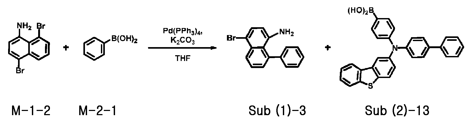

(1) Sub (1)-3 합성
M-1-2 (9.03 g, 30 mmol), M-2-1 (3.66 g, 30 mmol), Pd(PPh3)4 (1.04 g, 0.9 mmol), K2CO3 (3.6 g, 90 mmol), 무수 THF(132 mL), 소량의 물 (66 mL)을 상기 Sub (3)-1 합성법을 사용하여 생성물 6.17 g (수율: 69 %)를 얻었다.
(2) Sub (3)-13 합성
Sub (1)-3 (6.17 g, 20.7 mmol), Sub (2)-13 (9.75 g, 20.7 mmol), Pd(PPh3)4 (0.72 g, 0.62 mmol), K2CO3 (2.48 g, 62 mmol), 무수 THF(91 mL), 소량의 물(45 mL)을 상기 Sub (3)-1 합성법을 사용하여 생성물 9.07 g (수율: 68 %)를 얻었다.
(3) Sub 1-13 합성
Sub (3)-13 (9.07 g, 14 mmol), DMSO (70 mL) , CuI (4 g, 21 mmol)을 상기 Sub 1-1 합성 방법을 사용하여 생성물 1.16 g (수율: 38 %)을 얻었다.
3. Sub 1-20 합성예
<반응식 5> L3= H, n=0이고, m=1 일 때

(1) Sub (3)-20 합성
M-1-1 (6.66 g, 30 mmol), M-2-2 (13.2 g, 30 mmol), Pd(PPh3)4 (1.04 g, 0.9 mmol), K2CO3 (3.6 g, 90 mmol), 무수 THF(132 mL), 소량의 물 (66 mL)을 상기 Sub (3)-1 합성법을 사용하여 생성물 10.2 g (수율: 63 %)를 얻었다.
(2) Sub 1-20 합성
Sub (3)-20 (10.2 g, 14 mmol), DMSO (95 mL) , CuI (5.4 g, 28.4 mmol)을 상기 Sub 1-1 합성 방법을 사용하여 생성물 3.56 g (수율: 35 %)을 얻었다.
4. Sub 1-16 합성예
<반응식 6> n=1 이고, m=1 일 때

(1) Sub (1)-16 합성
M-1-3 (13.9 g, 30 mmol), M-2-3 (11 g, 30 mmol), Pd(PPh3)4 (1.04 g, 0.9 mmol), K2CO3 (3.6 g, 90 mmol), 무수 THF(132 mL), 소량의 물 (66 mL)을 상기 Sub (3)-1 합성법을 사용하여 생성물 14.38 g (수율: 68 %)를 얻었다.
(2) Sub 1-16 합성
Sub (3)-16 (14.38 g, 20.4 mmol), DMSO (102 mL) , CuI (5.83 g, 30.6 mmol)을 상기 Sub 1-1 합성 방법을 사용하여 생성물 5.6 g (수율: 39 %)을 얻었다.
5. Sub 1-21 합성예
<반응식 7> L2, L3= H, n=0 이고, m=0 일 때

(1) Sub (3)-21 합성
M-1-1 (6.66 g, 30 mmol), M-2-4 (5.16 g, 30 mmol), Pd(PPh3)4 (1.04 g, 0.9 mmol), K2CO3 (3.6 g, 90 mmol), 무수 THF(132 mL), 소량의 물(66 mL)을 상기 Sub (3)-1 합성법을 사용하여 생성물 5.25 g (수율: 65 %)를 얻었다.
(2) Sub 1-21 합성
Sub (3)-21 (5.25 g, 19.5 mmol), DMSO (97 mL) , CuI (5.57 g, 29.2 mmol)을 상기 Sub 1-1 합성 방법을 사용하여 생성물 1.77 g (수율: 34 %)을 얻었다.
6. Sub 1-23 합성예
<반응식 8> L2= H, n=1 이고, m=0 일 때

(1) Sub (3)-23 합성
M-1-3 (13.96 g, 30 mmol), M-2-4 (5.16 g, 30 mmol), Pd(PPh3)4 (1.04 g, 0.9 mmol), K2CO3 (3.6 g, 90 mmol), 무수 THF(132 mL), 소량의 물(66 mL)을 상기 Sub (3)-1 합성법을 사용하여 생성물 11.2 g (수율: 73 %)를 얻었다.
(2) Sub 1-23 합성
Sub (3)-23 (11.2 g, 22 mmol), DMSO (110 mL) , CuI (6.27 g, 33 mmol)을 상기 Sub 1-1 합성 방법을 사용하여 생성물 4.8 g (수율: 43 %)을 얻었다.
7. Sub 1-24 합성예
<반응식 9> L3= H, n=0 이고, m=1 일 때

(1) Sub (3)-24 합성
M-1-1 (6.66 g, 30 mmol), M-2-5 (10.18 g, 30 mmol), Pd(PPh3)4 (1.04 g, 0.9 mmol), K2CO3 (3.6 g, 90 mmol), 무수 THF(132 mL), 소량의 물(66 mL)을 상기 Sub (3)-1합성법을 사용하여 생성물 8.77 g (수율: 67 %)를 얻었다.
(3) Sub 1-24 합성
Sub (3)-24 (8.77 g, 20 mmol), DMSO (100 mL) , CuI (5.74 g, 30 mmol)을 상기 Sub 1-1 합성 방법을 사용하여 생성물 2.97 g (수율: 34 %)을 얻었다.
8. Sub 1-26 합성예
<반응식 10> n=1 이고, m=1 일 때

(1) Sub (3)-26 합성
M-1-4 (14 g, 30 mmol), M-2-5 (10.18 g, 30 mmol), Pd(PPh3)4 (1.04 g, 0.9 mmol), K2CO3 (3.6 g, 90 mmol), 무수 THF(132 mL), 소량의 물(66 mL)을 상기 Sub (3)-1합성법을 사용하여 생성물 14.4 g (수율: 71 %)를 얻었다.
(3) Sub 1-26 합성
Sub (3)-26 (14.5 g, 21.3 mmol), DMSO (106 mL) , CuI (6.09 g, 32 mmol)을 상기 Sub 1-1 합성 방법을 사용하여 생성물 5.2 g (수율: 36 %)을 얻었다.
9. Sub 1-31 합성예
<반응식 11> L2, L3= H, n=0 이고, m=0 일 때

(1) Sub (3)-31 합성
M-1-1 (6.66 g, 30 mmol), M-2-4 (5.16 g, 30 mmol), Pd(PPh3)4 (1.04 g, 0.9 mmol), K2CO3 (3.6 g, 90 mmol), 무수 THF(132 mL), 소량의 물(66 mL)을 상기 Sub (3)-1합성법을 사용하여 생성물 5.5 g (수율: 68 %)를 얻었다.
(2) Sub 1-31 합성
Sub (3)-31 (5.5 g, 20.4 mmol), DMSO (102 mL) , CuI (5.83 g, 30.6 mmol)을 상기 Sub 1-1 합성 방법을 사용하여 생성물 2.07 g (수율: 38 %)을 얻었다.
10. Sub 1-38 합성예
<반응식 12> L2= H, n=1 이고, m=0 일 때

(1) Sub (3)-38 합성
Sub M-1-4 (12.2 g, 22 mmol), M-2-4 (3.78 g, 22 mmol), Pd(PPh3)4 (0.76 g, 0.66 mmol), K2CO3 (2.63 g, 65.9 mmol), 무수 THF(96 mL), 소량의 물(48 mL)을 상기 Sub (3)-1합성법을 사용하여 생성물 8.34 g (수율: 63%)를 얻었다.
(2) Sub 1-38 합성
Sub (3)-38 (8.34 g, 13.8 mmol), DMSO (70 mL) , CuI (3.95 g, 20.8 mmol)을 상기 Sub 1-1 합성 방법을 사용하여 생성물 2.91 g (수율: 35 %)을 얻었다.
11. Sub 1-32 합성예
<반응식 13> L3= H, n=0 이고, m=1 일 때

(1) Sub (3)-32 합성
M-1-1 (6.66 g, 30 mmol), M-2-6 (15.9 g, 30 mmol), Pd(PPh3)4 (1.04 g, 0.9 mmol), K2CO3 (3.6 g, 90 mmol), 무수 THF(132 mL), 소량의 물(66 mL)을 상기 Sub (3)-1 합성법을 사용하여 생성물 14.7 g (수율: 65 %)를 얻었다.
(2) Sub 1-32 합성
Sub (3)-32 (14.7 g, 19.5 mmol), DMSO (98 mL), CuI (5.58 g, 29.3 mmol)을 상기 Sub 1-1 합성 방법을 사용하여 생성물 6.01 g (수율: 41 %)을 얻었다.
12. Sub 1-46 합성예
<반응식 14> n=1 이고, m=1 일 때

(1) Sub (3)-46 합성
M-1-4 (14 g, 30 mmol), M-2-7 (12.46 g, 30 mmol), Pd(PPh3)4 (1.04 g, 0.9 mmol), K2CO3 (3.6 g, 90 mmol), 무수 THF(132 mL), 소량의 물(66 mL)을 상기 Sub (3)-1 합성법을 사용하여 생성물 15.2 g (수율: 67 %)를 얻었다.
(2) Sub 1-46 합성
Sub (3)-46 (15.2 g, 20.1 mmol), DMSO (100 mL) , CuI (5.74 g, 30.2 mmol)을 상기 Sub 1-1 합성 방법을 사용하여 생성물 6.52 g (수율: 43 %)을 얻었다.
13. Sub 1-52 합성예
<반응식 15> L2, L3= H, n=0 이고, m=0 일 때

(1) Sub (3)-52 합성
M-1-1 (6.66 g, 30 mmol), M-2-4 (5.16 g, 30 mmol), Pd(PPh3)4 (1.04 g, 0.9 mmol), K2CO3 (3.6 g, 90 mmol), 무수 THF(132 mL), 소량의 물(66 mL)을 상기 Sub (3)-1합성법을 사용하여 생성물 5.74 g (수율: 71%)를 얻었다.
(2) Sub 1-52 합성
Sub (3)-52 (5.74 g, 21.3 mmol), DMSO (107 mL) , CuI (6.09 g, 32 mmol)을 상기 Sub 1-1 합성 방법을 사용하여 생성물 2.16 g (수율: 38 %)을 얻었다.
14. Sub 1-57 합성예
<반응식 16> L2= H, n=1 이고, m=0 일 때

(1) Sub (3)-57 합성
M-1-5 (17.14 g, 30 mmol), M-2-4 (5.16 g, 30 mmol), Pd(PPh3)4 (1.04 g, 0.9 mmol), K2CO3 (3.6 g, 90 mmol), 무수 THF(132 mL), 소량의 물(66 mL)을 상기 Sub (3)-1 합성법을 사용하여 생성물 5.74 g (수율: 65%)를 얻었다.
(2) Sub 1-57 합성
Sub (3)-57 (5.74 g, 21.3 mmol), DMSO (46 mL) , CuI (2.65 g, 14 mmol)을 상기 Sub 1-1 합성 방법을 사용하여 생성물 2.29 g (수율: 40 %)을 얻었다.
15. Sub 1-56 합성예
<반응식 17> L3= H, n=0 이고, m=1 일 때

(1) Sub (3)-56 합성
M-1-1 (6.66 g, 30 mmol), M-2-8 (12.46 g, 30 mmol), Pd(PPh3)4 (1.04 g, 0.9 mmol), K2CO3 (3.6 g, 90 mmol), 무수 THF(132 mL), 소량의 물(66 mL)을 상기 Sub (3)-1 합성법을 사용하여 생성물 11.23 g (수율: 73%)를 얻었다.
(2) Sub 1-56 합성
Sub (3)-56 (11.23 g, 21.9 mmol), DMSO (109 mL) , CuI (6.26 g, 32.9 mmol)을 상기 Sub 1-1 합성 방법을 사용하여 생성물 4.25 g (수율: 38 %)을 얻었다.
16. Sub 1-60 합성예
<반응식 18> n=1 이고, m=1 일 때

(1) Sub (3)-60 합성
M-1-6 (17.4 g, 30 mmol), M-2-9 (12.46 g, 30 mmol), Pd(PPh3)4 (1.04 g, 0.9 mmol), K2CO3 (3.6 g, 90 mmol), 무수 THF(132 mL), 소량의 물(66 mL)을 상기 Sub (3)-1합성법을 사용하여 생성물 18.6 g (수율: 71%)를 얻었다.
(2) Sub 1-60 합성
Sub (3)-60 (18.6 g, 21.3 mmol), DMSO (107 mL) , CuI (6.09 g, 32 mmol)을 상기 Sub 1-1 합성 방법을 사용하여 생성물 6.5 g (수율: 35 %)을 얻었다.
하기 표 1은 Sub 1 에 속하는 화합물의 FD-MS 값을 나타낸 것이다.
[표 1]

II. Sub 2의 합성
상기 반응식 1의 Sub 2는 하기의 반응경로에 의해 합성될 수 있으나, 이에 한정되는 것은 아니다.
Sub 2 에 속하는 화합물은 아래와 같은 화합물일 수 있으나, 이에 한정되는 것은 아니다.


1. Sub 2-74
합성예
<반응식 19> L1 내지 L3이 단일결합인 경우

Sub (2)-I-5 (6.8 g, 35 mmol)를 메틸렌크로라이드(123 mL)에 녹인 후, NBS(N-bromosuccimide) (6.85 g, 38.5 mmol)를 서서히 첨가한 뒤, 상온에서 24시간 교반시킨다. 반응이 종료되면 5% 농도의 HCl을 첨가한 뒤, 물을 첨가하여 잔존 NBS를 제거한다. 그 후 ether와 물로 추출하고 유기층을 MgSO4로 건조하고 농축 한 후 생성된 유기물을 silicagel column 및 재결정하여 생성물 7.46 g (수율: 78 %)을 얻었다.
2. Sub 2-3 합성예
<반응식 20> L1 내지 L3이 단일결합이 아닌 경우

(1) Sub (2)-II-1 합성
aniline (2.8 g, 30 mmol)과 2-bromonaphthalene (6.83 g, 33 mmol)을 toluene (315 mL) 에 넣고 Pd2(dba)3 (1.37 g, 1.5 mmol), P(t-Bu)3 (0.6 g, 3 mmol), NaOt-Bu (8.65 g, 90 mmol)을 각각 첨가한 뒤, 100℃ 에서 24시간 교반 환류 시킨다. ether와 물로 추출한 후 유기층을 MgSO4로 건조하고 농축 한 후 생성된 유기물을 silicagel column 및 재결정하여 생성물 4.28 g(수율: 65%)를 얻었다.
(2) Sub 2-3 합성
Sub (2)-II-1 (4.28 g, 19.5 mmol), Sub (2)-III-1 (6.07 g, 21 mmol), toluene (204 mL), Pd2(dba)3 (0.89 g, 0.98 mmol), P(t-Bu)3 (0.39 g, 1.95 mmol), NaOt-Bu (5.63 g, 58.6 mmol) 을 상기 Sub (2)-II-1 합성법을 사용하여 생성물 4.53 g (수율: 62 %)를 얻었다.
3. Sub 2-43 합성예
<반응식 21> L1 내지 L3이 단일결합이 아닌 경우

(1) Sub (2)-II-43 합성
[1,1'-biphenyl]-4-amine (5.07 g, 30 mmol), 2-bromo-9,9'-spirobi[fluorene] (13 g, 33 mmol), toluene (315 mL), Pd2(dba)3 (1.37 g, 1.5 mmol), P(t-Bu)3 (0.6 g, 3 mmpl), NaOt-Bu (8.65 g, 90 mmol) 을 상기 Sub (2)-II-1 합성법을 사용하여 생성물 12.2 g (수율: 68 %)를 얻었다.
(2) Sub 2-43 합성
Sub (2)-II-43 (12.2 g, 25.2 mmol), Sub (2)-III-1 (7.85 g, 27.8 mmol), toluene (264 mL), Pd2(dba)3 (1.16 g, 1.26 mmol), P(t-Bu)3 (0.51 g, 2.5 mmol), NaOt-Bu (7.27 g, 75.7 mmol) 을 상기 Sub (2)-II-1 합성법을 사용하여 생성물 10.3 g (수율: 64 %)를 얻었다.
4. Sub 2-61 합성예
<반응식 22> L1 내지 L3이 단일결합이 아닌 경우

(1) Sub (2)-II-61 합성
[1,1'-biphenyl]-3-amine (5.08 g, 30 mmol), 2-bromodibenzo[b,d]furan (8.15 g, 33 mmol), toluene (315 mL), Pd2(dba)3 (1.37 g, 1.5 mmol), P(t-Bu)3 (0.6 g, 3 mmpl), NaOt-Bu (8.65 g, 90 mmol) 을 상기 Sub (2)-II-1 합성법을 사용하여 생성물 6.54 g (수율: 65 %)를 얻었다.
(2) Sub 2-61 합성
Sub (2)-II-61 (6.54 g, 16.4 mmol), Sub (2)-III-3 (6.83 g, 18 mmol), toluene (172 mL), Pd2(dba)3 (0.75 g, 0.82 mmol), P(t-Bu)3 (0.33 g, 1.64 mmol), NaOt-Bu (4.72 g, 49 mmol) 을 상기 Sub (2)-II-1 합성법을 사용하여 생성물 7.16 g (수율: 72 %)를 얻었다.
하기 표 2는 Sub 2 에 속하는 화합물의 FD-MS 값을 나타낸 것이다.
[표 2]


III. 최종 생성물(Final Products)의 합성
1. P 1-8 합성예
<반응식 23>

Sub 1-1 (6.52 g, 30 mmol)과 Sub 2-8 (14.5 g, 33 mmol)을 toluene (315 mL) 에 넣고 Pd2(dba)3 (1.37 g, 1.5 mmol), P(t-Bu)3 (0.6 g, 3 mmol), NaOt-Bu (8.65 g, 90 mmol)을 각각 첨가한 뒤, 100 ℃ 에서 24시간 교반 환류 시킨다. ether와 물로 추출한 후 유기층을 MgSO4로 건조하고 농축 한 후 생성된 유기물을 silicagel column 및 재결정하여 생성물 12.5 g(수율: 72%)를 얻었다.
2. P 1-75 합성예
<반응식 24>

Sub 1-8 (18.5 g, 30 mmol), Sub 2-93 (14.2 g, 33 mmol), toluene (315 mL), Pd2(dba)3 (1.37 g, 1.5 mmol), P(t-Bu)3 (0.61 g, 3 mmol), NaOt-Bu (8.65 g, 90 mmol) 을 상기 P 1-8 합성법을 사용하여 생성물 18.4 g (수율: 67 %)를 얻었다.
3. P 1-84 합성예
<반응식 25>

Sub 1-16 (21 g, 30 mmol), Sub 2-1 (10.7 g, 33 mmol), toluene (315 mL), Pd2(dba)3 (1.37 g, 1.5 mmol), P(t-Bu)3 (0.61 g, 3 mmol), NaOt-Bu (8.65 g, 90 mmol) 을 상기 P 1-8 합성법을 사용하여 생성물 17.31 g (수율: 61 %)를 얻었다.
4. P 2-40 합성예
<반응식 26>

Sub 1-30 (14.7 g, 25 mmol), Sub 2-78 (7.24 g, 27.5 mmol), toluene (263 mL), Pd2(dba)3 (1.14 g, 1.25 mmol), P(t-Bu)3 (0.51 g, 2.5 mmol), NaOt-Bu (7.21 g, 75 mmol) 을 상기 P 1-8 합성법을 사용하여 생성물 12.5 g (수율: 65 %)를 얻었다.
5. P 2-22 합성예
<반응식 27>

Sub 1-21 (8.02 g, 30 mmol), Sub 2-54 (18.2 g, 33 mmol), toluene (315 mL), Pd2(dba)3 (1.37 g, 1.5 mmol), P(t-Bu)3 (0.61 g, 3 mmol), NaOt-Bu (8.65 g, 90 mmol) 을 상기 P 1-8 합성법을 사용하여 생성물 15.3 g (수율: 69 %)를 얻었다.
6. P 2-33 합성예
<반응식 28>

Sub 1-24 (13 g, 30 mmol), Sub 2-63 (18.6 g, 33 mmol), toluene (315 mL), Pd2(dba)3 (1.37 g, 1.5 mmol), P(t-Bu)3(0.61 g, 3 mmol), NaOt-Bu (8.65 g, 90 mmol) 을 상기 P 1-8 합성법을 사용하여 생성물 20.1 g (수율: 73 %)를 얻었다.
7. P 2-38 합성예
<반응식 29>

Sub 1-28 (18.8 g, 25 mmol), Sub 2-70 (5.7 g, 27.5 mmol), toluene (263 mL), Pd2(dba)3 (1.14 g, 1.25 mmol), P(t-Bu)3 (0.51 g, 2.5 mmol), NaOt-Bu (7.21 g, 75 mmol) 을 상기 P 1-8 합성법을 사용하여 생성물 15.8 g (수율: 72 %)를 얻었다.
8. P 3-41 합성예
<반응식 30>

Sub 1-31 (8 g, 30 mmol), Sub 2-39 (15.7 g, 33 mmol), toluene (315 mL), Pd2(dba)3 (1.37 g, 1.5 mmol), P(t-Bu)3 (0.61 g, 3 mmol), NaOt-Bu (8.65 g, 90 mmol) 을 상기 P 1-8 합성법을 사용하여 생성물 14.5 g (수율: 73 %)를 얻었다.
9. P 3-53 합성예
<반응식 31>

Sub 1-33 (5.3 g, 20 mmol), Sub 2-51 (13.3 g, 22 mmol), toluene (210 mL), Pd2(dba)3 (0.92 g, 1 mmol), P(t-Bu)3 (0.4 g, 2 mmol), NaOt-Bu (5.77 g, 60 mmol) 을 상기 P 1-8 합성법을 사용하여 생성물 14.2 g (수율: 73 %)를 얻었다.
10. P 3-87 합성예
<반응식 32>

Sub 1-50 (12.3 g, 20 mmol), Sub 2-75 (6 g, 22 mmol), toluene (210 mL), Pd2(dba)3 (0.92 g, 1 mmol), P(t-Bu)3 (0.4 g, 2 mmol), NaOt-Bu (5.77 g, 60 mmol) 을 상기 P 1-8 합성법을 사용하여 생성물 10.4 g (수율: 64 %)를 얻었다.
11. P 3-84 합성예
<반응식 33>

Sub 1-47 (15.1 g, 20 mmol), Sub 2-1 (7.1 g, 22 mmol), toluene (210 mL), Pd2(dba)3 (0.92 g, 1 mmol), P(t-Bu)3 (0.4 g, 2 mmol), NaOt-Bu (5.77 g, 60 mmol) 을 상기 P 1-8 합성법을 사용하여 생성물 12.2 g (수율: 61 %)를 얻었다.
12. P 4-32 합성예
<반응식 34>

Sub 1-52 (8 g, 30 mmol), Sub 2-55 (19.2 g, 33 mmol), toluene (315 mL), Pd2(dba)3 (1.37 g, 1.5 mmol), P(t-Bu)3 (0.61 g, 3 mmol), NaOt-Bu (8.65 g, 90 mmol) 을 상기 P 1-8 합성법을 사용하여 생성물 15 g (수율: 65 %)를 얻었다.
13. P 4-45 합성예
<반응식 35>

Sub 1-57 (18.5 g, 30 mmol), Sub 2-1 (10.7 g, 33 mmol), toluene (315 mL), Pd2(dba)3 (1.37 g, 1.5 mmol), P(t-Bu)3 (0.61 g, 3 mmol), NaOt-Bu (8.65 g, 90 mmol) 을 상기 P 1-8 합성법을 사용하여 생성물 16.3 g (수율: 63 %)를 얻었다.
14. P 4-48 합성예
<반응식 36>

Sub 1-60 (17.4 g, 20 mmol), Sub 2-68 (3.45 g, 22 mmol), toluene (210 mL), Pd2(dba)3 (0.92 g, 1 mmol), P(t-Bu)3 (0.4 g, 2 mmol), NaOt-Bu (5.77 g, 60 mmol) 을 상기 P 1-8 합성법을 사용하여 생성물 12.3 g (수율: 65 %)를 얻었다.
한편, 상기와 같은 합성예에 따라 제조된 본 발명의 화합물 P 1-1 내지 P 1-84, P 2-1 내지 P 2-40, P 3-1 내지 P 3-88, P 4-1 내지 P 4-52 의 FD-MS 값은 하기 표 3과 같다.
[표 3]


유기전기소자의 제조평가
[실시예 1] 그린유기전기발광소자 (정공수송층)
본 발명의 화합물을 정공수송층 물질로 사용하여 통상적인 방법에 따라 유기전기발광소자를 제작하였다. 먼저, 유기 기판에 형성된 ITO층(양극) 상에 4,4',4''-Tris[2-naphthyl(phenyl)amino]triphenylamine (이하 "2-TNATA"로 약기함)을 60 nm 두께로 진공증착하여 정공주입층을 형성한 후, 상기 정공주입층 상에 본 발명의 화합물 P 1-1 을 60 nm 두께로 진공증착하여 정공수송층을 형성하였다. 이어서, 상기 정공수송층 상에 4,4'-N,N'-dicarbazole-biphenyl (이하, "CBP"로 약기함)을 호스트 물질로, tris(2-phenylpyridine)-iridium (이하, "Ir(ppy)3"으로 약기함)을 도판트 물질로 사용하고 90:10 중량비로 도핑하여 30nm 두께로 진공증착하여 발광층을 형성하였다. 이어서 상기 발광층 상에 (1,1'-비스페닐)-4-올레이토)비스(2-메틸-8-퀴놀린올레이토)알루미늄 (이하 "BAlq"로 약기함)을 10 nm 두께로 진공증착하여 정공저지층을 형성하고, 상기 정공저지층 상에 트리스(8-퀴놀리놀)알루미늄 (이하 "Alq3"로 약기함)을 40 nm 두께로 진공증착하여 전자수송층을 형성하였다. 이후, 할로젠화 알칼리 금속인 LiF를 0.2 nm 두께로 증착하여 전자주입층을 형성하고, 이어서 Al을 150 nm의 두께로 증착하여 음극을 형성함으로써 유기전기발광소자를 제조하였다.
[실시예 2] 내지 [실시예 176] 그린유기전기발광소자 (정공수송층)
정공 수송층 물질로 본 발명의 화합물 P 1-1 대신 하기 표 4에 기재된 본 발명의 화합물을 사용한 점을 제외하고는 실시예 1과 동일한 방법으로 유기전기발광소자를 제작하였다.
[비교예 1]
비교예 1은 정공수송층 물질로 본 발명의 화합물 P 1-1 대신 하기 비교화합물 1을 사용한 점을 제외하고는 상기 실시예 1과 동일한 방법으로 유기전기발광소자를 제조하였다.

[비교예 2]
비교예 2는 정공수송층 물질로 본 발명의 화합물 P 1-1 대신 하기 비교화합물 2를 사용한 점을 제외하고는 상기 실시예 1과 동일한 방법으로 유기전기발광소자를 제조하였다.

이와 같이 제조된 실시예 및 비교예 유기전기발광소자들에 순바이어스 직류전압을 가하여 포토리서치(photoresearch)사의 PR-650으로 전기발광(EL) 특성을 측정하였으며, 그 측정 결과 5000cd/m2 기준 휘도에서 맥사이언스사에서 제조된 수명 측정 장비를 통해 T95 수명을 측정하였다. 하기 표 4는 소자제작 및 평가한 결과를 나타낸다.
[표 4] 그린유기전기발광소자의 제작 및 시험 (정공수송층)


상기 표 4의 결과로부터 알 수 있듯이, 본 발명의 화합물을 정공수송층의 재료로 사용한 유기전기발광소자가 비교화합물 1, 비교화합물 2보다 낮은 구동전압과 비교적 높은 효율 그리고 높은 수명을 나타내는 것을 확인하였다.
특히 자사 발명화합물과 코어적으로 유사한 구조인 비교화합물 2의 경우 효율은 비교적 높게 나타내고 있으나, 수명은 자사 발명화합물에 비해 현저히 낮게 나타났다.
이는 소자 구동 초기에는 비교화합물 2와 자사 발명화합물의 소자적 수명이 유사하게 나타나다가 소자의 수명이 급 감소되는 경우로 판단되며, 대부분 이런 경우 joule heat(열적 데미지 발생)로 인한 소자 수명 감소 또는 발광층 내 charge balance불균형으로 인해 발생되는 것이라 판단된다. 또한 자사 발명화합물의 소자 측정 결과에서 알 수 있듯이, 자사 발명화합물의 코어에 아민기의 결합 개수에 따른 성능적 차이를 발견할 수 있었다. 이는 아민기의 개수가 증가됨에 따라 분자 내 rotation point가 많아지고 이로인해 packing density가 감소하여 정공의 이동이 떨어지게 되는 것으로 판단된다.
[실시예 177] 그린유기전기발광소자 (발광보조층)
먼저, 유리 기판에 형성된 ITO층(양극) 위에 우선 홀 주입층으로서 N1-(naphthalen-2-yl)-N4,N4-bis(4-(naphthalen-2-yl(phenyl)amino)phenyl)-N1-phenylbenzene-1,4-diamine (이하 "2-TNATA"로 약기함) 막을 진공증착하여 60 nm 두께로 형성하였다. 이어서, 이 막 상에 정공수송 화합물로서 4,4-비스[N-(1-나프틸)-N-페닐아미노]비페닐 (이하 "-NPD"로 약기함)을 60 nm 두께로 진공증착하여 홀 수송층을 형성하였다. 이어서, 발광보조층 재료로서 상기 발명 화합물 P 1-59를 20nm의 두께로 진공증착하여 발광보조층을 형성하였다. 발광보조층을 형성한 후, 발광보조층 상부에 호스트로서는 CBP[4,4'-N,N'-dicarbazole-biphenyl]를 사용하였으며, 도판트로서는 Ir(ppy)3 [tris(2-phenylpyridine)-iridium]를 95:5 중량으로 도핑함으로써 상기 발광보조층 위에 30nm 두께의 발광층을 증착하였다. 홀 저지층으로 (1,1'-비스페닐)-4-올레이토)비스(2-메틸-8-퀴놀린올레이토)알루미늄(이하 "BAlq"로 약기함)을 10 nm 두께로 진공증착하고, 전자수송층으로 트리스(8-퀴놀리놀)알루미늄(이하 "Alq3"로 약기함)을 40 nm 두께로 성막하였다. 이후, 전자주입층으로 할로젠화 알칼리 금속인 LiF를 0.2 nm 두께로 증착하고, 이어서 Al을 150 nm의 두께로 증착하여 음극으로 사용함으로서 유기전기발광소자를 제조하였다.
[실시예 178] 내지 [실시예 204] 그린유기전기발광소자 (발광보조층)
발광보조층 물질로 본 발명의 화합물 P 1-59 대신 하기 표5에 기재된 본 발명의 화합물을 사용한 점을 제외하고는 실시예 177과 동일한 방법으로 유기전기발광소자를 제작하였다.
[비교예 3]
비교예 3은 발광보조층을 사용하지 않은 점을 제외하고는 상기 실시예 177과 동일한 방법으로 유기전기발광소자를 제작하였다.
[비교예 4]
비교예 4는 본 발명의 화합물 P 1-59 대신 상기 비교화합물 1을 사용한 것을 제외하고는 상기 실시예 177과 동일한 방법으로 유기전기발광소자를 제작하였다.
[비교예 5]
비교예 5는 본 발명의 화합물 P 1-59 대신 상기 비교화합물 2를 사용한 것을 제외하고는 상기 실시예 177과 동일한 방법으로 유기전기발광소자를 제작하였다.
이와 같이 제조된 실시예 및 비교예 유기전기발광소자들에 순바이어스 직류전압을 가하여 포토리서치(photoresearch)사의 PR-650으로 전기발광(EL) 특성을 측정하였으며, 그 측정 결과 5000cd/m2 기준 휘도에서 맥사이언스사에서 제조된 수명 측정 장비를 통해 T95 수명을 측정하였다. 하기 표 5는 소자제작 및 평가한 결과를 나타낸다.
[표 5] 그린유기전기발광소자의 제작 및 시험 (발광보조층)


[실시예 205] 레드유기전기발광소자 (발광보조층)
먼저, 유리 기판에 형성된 ITO층(양극) 위에 우선 홀 주입층으로서 N1-(naphthalen-2-yl)-N4,N4-bis(4-(naphthalen-2-yl(phenyl)amino)phenyl)-N1-phenylbenzene-1,4-diamine (이하 "2-TNATA"로 약기함) 막을 진공증착하여 60 nm 두께로 형성하였다. 이어서, 이 막 상에 정공수송 화합물로서 4,4-비스[N-(1-나프틸)-N-페닐아미노]비페닐 (이하 "-NPD"로 약기함)을 20 nm 두께로 진공증착하여 홀 수송층을 형성하였다. 이어서, 발광보조층 재료로서 본 발명의 화합물 P 1-52를 60nm의 두께로 진공증착하여 발광보조층을 형성하였다. 발광보조층을 형성한 후, 발광보조층 상부에 호스트로서는 CBP[4,4'-N,N'-dicarbazole-biphenyl]를 사용하였으며, 도판트로서는 (piq)2Ir(acac) [bis-(1-phenylisoquinolyl)iridium(Ⅲ)acetylacetonate]을 95:5 중량으로 도핑함으로써 상기 발광보조층 위에 30nm 두께의 발광층을 증착하였다. 홀 저지층으로 (1,1'-비스페닐)-4-올레이토)비스(2-메틸-8-퀴놀린올레이토)알루미늄(이하 "BAlq"로 약기함)을 10 nm 두께로 진공증착하고, 전자수송층으로 트리스(8-퀴놀리놀)알루미늄(이하 "Alq3"로 약기함)을 40 nm 두께로 성막하였다. 이후, 전자주입층으로 할로젠화 알칼리 금속인 LiF를 0.2 nm 두께로 증착하고, 이어서 Al을 150 nm의 두께로 증착하여 음극으로 사용함으로서 유기전기발광소자를 제조하였다.
[실시예 206] 내지 [실시예 222] 레드유기전기발광소자 (발광보조층)
발광보조층 물질로 본 발명의 화합물 P 1-52 대신 하기 표 6에 기재된 본 발명의 화합물을 사용한 점을 제외하고는 실시예 205와 동일한 방법으로 유기전기발광소자를 제작하였다.
[비교예 6]
비교예 6은 발광보조층을 사용하지 않은 점을 제외하고는 상기 실시예 205와 동일한 방법으로 유기전기발광소자를 제작하였다.
[비교예 7]
비교예 7은 본 발명의 화합물 P 1-52 대신 상기 비교화합물 1을 사용한 것을 제외하고는 상기 실시예 205와 동일한 방법으로 유기전기발광소자를 제작하였다.
[비교예 8]
비교예 8은 본 발명의 화합물 P 1-52 대신 상기 비교화합물 2를 사용한 것을 제외하고는 상기 실시예 205과 동일한 방법으로 유기전기발광소자를 제작하였다.
이와 같이 제조된 실시예 및 비교예 유기전기발광소자들에 순바이어스 직류전압을 가하여 포토리서치(photoresearch)사의 PR-650으로 전기발광(EL) 특성을 측정하였으며, 그 측정 결과 2500cd/m2 기준 휘도에서 맥사이언스사에서 제조된 수명 측정 장비를 통해 T95 수명을 측정하였다. 하기 표 6은 소자제작 및 평가한 결과를 나타낸다.
[표 6] 레드유기전기발광소자의 제작 및 시험 (발광보조층)

[실시예 223] 블루유기전기발광소자 (발광보조층)
먼저, 유리 기판에 형성된 ITO층(양극) 위에 우선 홀 주입층으로서 N1-(naphthalen-2-yl)-N4,N4-bis(4-(naphthalen-2-yl(phenyl)amino)phenyl)-N1-phenylbenzene-1,4-diamine (이하 "2-TNATA"로 약기함) 막을 진공증착하여 60 nm 두께로 형성하였다. 이어서, 이 막 상에 정공수송 화합물로서 4,4-비스[N-(1-나프틸)-N-페닐아미노]비페닐 (이하 "-NPD"로 약기함)를 60 nm 두께로 진공증착하여 홀 수송층을 형성하였다. 이어서, 발광보조층 재료로서 본 발명의 화합물인 P 1-4를 20nm의 두께로 진공증착하여 발광보조층을 형성하였다. 발광보조층을 형성한 후, 발광보조층 상부에 호스트로서는 9,10-di(naphthalen-2-yl)anthracene, 도판트로서는 BD-052X(Idemitsu kosan) 을 93:7 중량으로 도핑함으로써 상기 발광보조층 위에 30nm 두께의 발광층을 증착하였다. 홀 저지층으로 (1,1'-비스페닐)-4-올레이토)비스(2-메틸-8-퀴놀린올레이토)알루미늄(이하 "BAlq"로 약기함)을 10 nm 두께로 진공증착하고, 전자수송층으로 트리스(8-퀴놀리놀)알루미늄(이하 "Alq3"로 약칭함)을 40 nm 두께로 성막하였다. 이후, 전자주입층으로 할로젠화 알칼리 금속인 LiF를 0.2 nm 두께로 증착하고, 이어서 Al을 150 nm의 두께로 증착하여 음극으로 사용함으로서 유기전기발광소자를 제조하였다.
[실시예 224] 내지 [실시예 275] 블루유기전기발광소자 (발광보조층)
발광보조층 물질로 본 발명의 화합물 P 1-4 대신 하기 표 7에 기재된 본 발명의 화합물을 사용한 점을 제외하고는 실시예 223과 동일한 방법으로 유기전기발광소자를 제작하였다.
[비교예 9]
비교예9는 발광보조층을 사용하지 않은 것을 제외하고는 상기 실시예 223과 동일한 방법으로 유기전기발광소자를 제작하였다.
[비교예 10]
비교예 10은 본 발명의 화합물 P 1-4 대신 비교화합물 1을 사용한 것을 제외하고는 상기 실시예 223와 동일한 방법으로 유기전기발광소자를 제작하였다.
[비교예 11]
비교예 11은 본 발명의 화합물 P 1-4 대신 비교화합물 2를 사용한 것을 제외하고는 상기 실시예 223와 동일한 방법으로 유기전기발광소자를 제작하였다.
이와 같이 제조된 실시예 및 비교예 유기전기발광소자들에 순바이어스 직류전압을 가하여 포토리서치(photoresearch)사의 PR-650으로 전기발광(EL) 특성을 측정하였으며, 그 측정 결과 500cd/m2 기준 휘도에서 맥사이언스사에서 제조된 수명 측정 장비를 통해 T95 수명을 측정하였다. 하기 표 7은 소자제작 및 평가한 결과를 나타낸다.
[표 7] 블루유기전기발광소자의 제작 및 시험 (발광보조층)


[실시예 276] 그린유기전기발광소자 (정공수송층+발광보조층)
본 발명의 화합물을 정공수송층 물질로 사용하여 통상적인 방법에 따라 유기전기발광소자를 제작하였다. 먼저, 유리 기판에 형성된 ITO층(양극) 위에 우선 홀 주입층으로서 N1-(naphthalen-2-yl)-N4,N4-bis(4-(naphthalen-2-yl(phenyl)amino)phenyl)-N1-phenylbenzene-1,4-diamine (이하 "2-TNATA"로 약기함) 막을 진공증착하여 60 nm 두께로 형성하였다. 상기 정공주입층 상에 본 발명의 화합물 P 1-40 을 60 nm 두께로 진공증착하여 정공수송층을 형성하였다. 이어서, 발광보조층 재료로서 본 발명의 화합물 (P 1-59 외 12종)을 20nm의 두께로 진공증착하여 발광보조층을 형성하였다. 발광보조층을 형성한 후, 발광보조층 상부에 호스트로서는 CBP[4,4'-N,N'-dicarbazole-biphenyl]를 사용하였으며, 도판트로서는 Ir(ppy)3 [tris(2-phenylpyridine)-iridium]를 95:5 중량으로 도핑함으로써 상기 발광 보조층 위에 30nm 두께의 발광층을 증착하였다. 홀 저지층으로 (1,1'-비스페닐)-4-올레이토)비스(2-메틸-8-퀴놀린올레이토)알루미늄(이하 "BAlq"로 약기함)을 10 nm 두께로 진공증착하고, 전자수송층으로 트리스(8-퀴놀리놀)알루미늄(이하 "Alq3"로 약칭함)을 40 nm 두께로 성막하였다. 이후, 전자주입층으로 할로젠화 알칼리 금속인 LiF를 0.2 nm 두께로 증착하고, 이어서 Al을 150 nm의 두께로 증착하여 음극으로 사용함으로서 유기전기발광소자를 제조하였다.
[실시예 277] 내지 [실시예 288] 그린유기전기발광소자 (정공수송층+발광보조층)
발광보조층 물질로 본 발명의 화합물 P 1-59 대신 하기 표 8에 기재된 본 발명의 화합물을 사용한 점을 제외하고는 실시예 276과 동일한 방법으로 유기전기발광소자를 제작하였다.
이와 같이 제조된 실시예 및 비교예 유기전기발광소자들에 순바이어스 직류전압을 가하여 포토리서치(photoresearch)사의 PR-650으로 전기발광(EL) 특성을 측정하였으며, 그 측정 결과 5000cd/m2 기준 휘도에서 맥사이언스사에서 제조된 수명 측정 장비를 통해 T95 수명을 측정하였다. 하기 표 8은 소자제작 및 평가한 결과를 나타낸다.
[표 8] 그린유기전기발광소자의 제작 및 시험 (정공수송층+발광보조층)

상기 표 5, 표 6, 표 7, 표 8의 결과로부터 알 수 있듯이, 본 발명의 유기전기발광소자용 재료를 발광보조층으로 사용할 경우 발광효율 및 수명을 현저히 개선시키는 것을 확인 할 수 있었으며, 본 발명 화합물을 정공수송층과 발광보조층으로 사용했을 경우 수명이 현저히 개선되는 것을 확인 할 수 있었다.
다시 말해, 발광보조층을 쓰지 않았을 때보다 발광보조층을 사용하였을 때, 효율 및 수명이 상승 되었음을 확인할 수 있었으며, 비교화합물 1, 2 보다는 자사 발명화합물이 발광보조층으로 사용되었을 시, 더 높은 효율과 더 높은 수명을 나타내는 것을 확인하였다.
발광보조층으로 자사 발명화합물을 사용했을 경우 더 높은 효율의 증가가 일어나는 이유로는 깊은 HOMO 에너지 레벨로 인하여, 정공이 발광층 내 과잉공급 되는 것을 감소 시킴으로써, 발광층 내 charge balance 를 증가시키게 되고, 과잉의 정공이 전자수송층으로 넘어가는 것을 감소시키게 되어 효율이 증가되는 것이라 판단된다.
또한 비교적 높은 T1을 가지고 있어, 정공수송층으로 넘어오는 과잉의 전자를 막아줌으로써 색순도 저하 및 정공수송층에서의 발광으로 인한 열적 데미지를 감소시켜 수명이 증가 되는 것으로 판단된다.
비교화합물 1, 2를 사용한 발광보조층으로 사용한 비교예 4, 5, 7, 8, 10, 11 의 결과를 확인해 보면, 발광보조층을 사용하지 않았을 때보다 효율 및 수명은 소폭 상승하지만 구동전압이 높아지는 현상을 확인할 수 있었다.
마지막으로 비교적 구동전압이 낮고 효율이 높은 자사 발명화합물 P 1-40을 정공수송층에 사용하고 본 발명 화합물인 P 1-59 외 12종 화합물을 발광보조층을 사용하였을 경우 비교화합물 1를 정공수송층으로 사용하였을 때보다 수명이 증가하는 것을 표 5와 표 8의 비교를 통해 확인할 수 있었다.
아울러, 전술한 소자 제작의 평가 결과에서는 전공수송층과 발광보조층 관점에서 소자 특성을 설명하였으나, 통상적으로 정공수송층과 발광보조층으로 사용되는 재료들은 전술한 전자수송층, 전자주입층, 정공주입층 및 발광층 등 유기전기소자의 유기물층으로 단일 또는 다른 재료와 혼합으로 사용될 수 있다. 따라서 전술한 이유로 본 발명의 화합물은 정공수송층과 발광보조층 이외에 다른 유기물층, 예를 들어 전자수송층, 전자주입층, 정공주입층 및 발광층 등에 단일 또는 다른 재료와 혼합으로 사용될 수 있다.
이상의 설명은 본 발명을 예시적으로 설명한 것에 불과한 것으로, 본 발명에 속하는 기술분야에서 통상의 지식을 가지는 자라면 본 발명의 본질적인 특성에서 벗어나지 않는 범위에서 다양한 변형이 가능할 것이다. 따라서, 본 명세서에 개시된 실시예들은 본 발명을 한정하기 위한 것이 아니라 설명하기 위한 것이고, 이러한 실시예에 의하여 본 발명의 사상과 범위가 한정되는 것은 아니다. 본 발명의 보호범위는 아래의 청구범위에 의하여 해석되어야 하며, 그와 동등한 범위내에 모든 기술은 본 발명의 권리범위에 포함하는 것으로 해석되어야 할 것이다.
부호의 설명
100: 유기전기소자 110: 기판
120: 제 1전극 130: 정공주입층
140: 정공수송층 141: 버퍼층
150: 발광층 151: 발광보조층
160: 전자수송층 170: 전자주입층
180: 제 2전극
CROSS-REFERENCE TO RELATED APPLICATION
본 특허출원은 2014년 07월 03일 한국에 출원한 특허출원번호 제 10-2014-0083017 호에 대해 미국 특허법 119(a)조 (35 U.S.C § 119(a))에 따라 우선권을 주장하며, 그 모든 내용은 참고문헌으로 본 특허출원에 병합된다. 아울러, 본 특허출원은 미국 이외에 국가에 대해서도 위와 동일한 이유로 우선권을 주장하면 그 모든 내용은 참고문헌으로 본 특허출원에 병합된다
Claims (10)
- 하기 화학식 1로 표시되는 화합물<화학식 1>
 [상기 화학식 1에서,A 환은 C6~C30의 단일환 또는 다환;이고,R1 내지 R6는 서로 동일하거나 상이하며, 서로 독립적으로 수소; 중수소; 할로겐; C6~C60의 아릴기; 플루오렌일기; O, N, S, Si 및 P 중 적어도 하나의 헤테로원자를 포함하는 C2~C60의 헤테로고리기; C3~C60의 지방족고리와 C6~C60의 방향족고리의 융합고리기; C1~C50의 알킬기; C2~C20의 알켄일기; C2~C20의 알킨일기; C1~C30의 알콕실기; C6~C30의 아릴옥시기; 및 -L'-N(Ra)(Rb);로 이루어진 군에서 선택되고, 또한 R1과 R2 또는 R3과 R4 또는 R5와 R6은 서로 결합하여 고리를 형성할 수 있으며,상기 L'은 단일결합; C6~C60의 아릴렌기; 플루오렌일렌기; C3~C60의 지방족고리와 C6~C60의 방향족고리의 융합고리기; 및 C2~C60의 헤테로고리기;로 이루어진 군에서 선택되고,상기 Ra 및 Rb는 서로 독립적으로 C6~C60의 아릴기; 플루오렌일기; C3~C60의 지방족고리와 C6~C60의 방향족고리의 융합고리기; 및 O, N, S, Si 및 P 중 적어도 하나의 헤테로원자를 포함하는 C2~C60의 헤테로고리기;로 이루어진 군에서 선택되며,o, m 및 n은 서로 독립적으로 0 또는 1이고, m+n+o≥1이고,상기 화학식 1에서 A 환이 벤젠이고 n, o가 모두 0이며 m이 1일 경우 R1, R2가 각각 비페닐, 다이벤조퓨란, 다이벤조싸이오펜, 플루오렌인 경우는 제외되고,L1 내지 L3가 o, m, n이 각각 0일 경우 L1, L2, L3는 수소; 아릴기; 플루오렌일기; O, N, S, Si 및 P 중 적어도 하나의 헤테로원자를 포함하는 C2~C60의 헤테로고리기;로 이루어진 군에서 선택되며,o, m, n이 각각 1일 경우 L1, L2, L3는 서로 독립적으로 단일결합; 아릴렌기; 플루오렌일렌기; C3~C60의 지방족고리와 C6~C60의 방향족고리의 융합고리기; 및 O, N, S, Si 및 P 중 적어도 하나의 헤테로원자를 포함하는 C2~C60의 2가의 헤테로고리기;로 이루어진 군에서 선택되고,상기 아릴기, 플루오렌일기, 헤테로고리기, 융합고리기, 알킬기, 알켄일기, 알킨일기, 알콕실기, 아릴옥시기, 아릴렌기 및 플루오렌일렌기 각각은 중수소; 할로겐; 실란기; 실록산기; 붕소기; 게르마늄기; 시아노기; 니트로기; C1~C20의 알킬싸이오기; C1~C20의 알콕실기; C1~C20의 알킬기; C2~C20의 알켄일기; C2~C20의 알킨일기; C6~C20의 아릴기; 중수소로 치환된 C6~C20의 아릴기; 플루오렌일기; C2~C20의 헤테로고리기; C3~C20의 시클로알킬기; C7~C20의 아릴알킬기; 및 C8~C20의 아릴알켄일기;로 이루어진 군에서 선택된 하나 이상의 치환기로 치환될 수 있다.
 - 제1항에 있어서,상기 A 환은 벤젠 또는 나프탈렌인 것을 특징으로 하는 화합물.
- 제 1항에 있어서,상기 화학식 1은 하기 화학식 중 하나로 표시되는 것을 특징으로 하는 화합물.

 (화학식 2 내지 화학식 5에서, R1 내지 R6, L1 내지 L3, m, n 및 o는 상기 화학식 1에서 정의된 R1 내지 R6, L1 내지 L3, m, n 및 o와 같음)
 - 제 1항에 있어서,하기 화합물 중 하나인 것을 특징으로 하는 화합물


- 제 1전극;제 2전극; 및상기 제 1전극과 제 2전극 사이에 위치하며, 제 1항 내지 제 4항 중 어느 한 항의 화합물을 함유하는 유기물층;을 포함하는 유기전기소자.
- 제 5항에 있어서,상기 화합물은 상기 유기물층의 정공주입층, 정공수송층, 발광보조층 및 발광층 중 적어도 하나의 층에 함유되어 있으며, 상기 화합물은 동종의 화합물 또는 2 이상의 이종의 화합물인 것을 특징으로 하는 유기전기소자.
- 제 5항에 있어서,상기 제 1전극과 제 2전극의 일면 중 상기 유기물층과 반대되는 적어도 일면에 형성되는 광효율 개선층을 더 포함하는 유기전기소자.
- 제 5항에 있어서,상기 유기물층은 스핀코팅 공정, 노즐 프린팅 공정, 잉크젯 프린팅 공정, 슬롯코팅 공정, 딥코팅 공정 또는 롤투롤 공정에 의해 형성되는 것을 특징으로 하는 유기전기소자.
- 제 5항의 유기전기소자를 포함하는 디스플레이장치; 및상기 디스플레이장치를 구동하는 제어부;를 포함하는 전자장치.
- 제 9항에 있어서,상기 유기전기소자는 유기전기발광소자, 유기태양전지, 유기감광체, 유기트랜지스터 및 단색 또는 백색 조명용 소자 중 하나인 것을 특징으로 하는 전자장치.
Priority Applications (2)
| Application Number | Priority Date | Filing Date | Title |
|---|---|---|---|
| US15/323,052 US10297758B2 (en) | 2014-07-03 | 2015-07-01 | Compound for organic electronic element, organic electronic element using same, and electronic device comprising same |
| US16/261,050 US11088330B2 (en) | 2014-07-03 | 2019-01-29 | Compound for organic electronic element, organic electronic element using same, and electronic device comprising same |
Applications Claiming Priority (2)
| Application Number | Priority Date | Filing Date | Title |
|---|---|---|---|
| KR10-2014-0083017 | 2014-07-03 | ||
| KR1020140083017A KR102277659B1 (ko) | 2014-07-03 | 2014-07-03 | 유기전기 소자용 화합물, 이를 이용한 유기전기소자 및 그 전자 장치 |
Related Child Applications (2)
| Application Number | Title | Priority Date | Filing Date |
|---|---|---|---|
| US15/323,052 A-371-Of-International US10297758B2 (en) | 2014-07-03 | 2015-07-01 | Compound for organic electronic element, organic electronic element using same, and electronic device comprising same |
| US16/261,050 Continuation US11088330B2 (en) | 2014-07-03 | 2019-01-29 | Compound for organic electronic element, organic electronic element using same, and electronic device comprising same |
Publications (2)
| Publication Number | Publication Date |
|---|---|
| WO2016003202A2 true WO2016003202A2 (ko) | 2016-01-07 |
| WO2016003202A3 WO2016003202A3 (ko) | 2016-08-11 |
Family
ID=55020064
Family Applications (1)
| Application Number | Title | Priority Date | Filing Date |
|---|---|---|---|
| PCT/KR2015/006784 Ceased WO2016003202A2 (ko) | 2014-07-03 | 2015-07-01 | 유기전기 소자용 화합물, 이를 이용한 유기전기소자 및 그 전자 장치 |
Country Status (3)
| Country | Link |
|---|---|
| US (2) | US10297758B2 (ko) |
| KR (2) | KR102277659B1 (ko) |
| WO (1) | WO2016003202A2 (ko) |
Cited By (3)
| Publication number | Priority date | Publication date | Assignee | Title |
|---|---|---|---|---|
| CN106632252A (zh) * | 2015-11-03 | 2017-05-10 | 三星显示有限公司 | 稠环化合物和包括该稠环化合物的有机发光装置 |
| CN107663191A (zh) * | 2016-07-27 | 2018-02-06 | 三星显示有限公司 | 多环化合物以及包括该多环化合物的有机发光装置 |
| US11407766B2 (en) | 2017-01-30 | 2022-08-09 | Merck Patent Gmbh | Materials for organic electroluminescent devices |
Families Citing this family (16)
| Publication number | Priority date | Publication date | Assignee | Title |
|---|---|---|---|---|
| WO2015178585A1 (ko) * | 2014-05-22 | 2015-11-26 | 덕산네오룩스 주식회사 | 유기전기 소자용 화합물, 이를 이용한 유기전기소자 및 그 전자 장치 |
| KR101745491B1 (ko) | 2015-03-12 | 2017-06-13 | 덕산네오룩스 주식회사 | 유기발광소자 및 유기발광 표시장치 |
| KR101984786B1 (ko) * | 2015-04-15 | 2019-05-31 | 주식회사 엘지화학 | 헤테로고리 화합물 및 이를 포함하는 유기 발광 소자 |
| KR102083707B1 (ko) * | 2016-02-11 | 2020-03-02 | 주식회사 엘지화학 | 화합물 및 이를 이용한 유기 전계 발광 소자 |
| KR102600472B1 (ko) * | 2016-09-13 | 2023-11-13 | 삼성디스플레이 주식회사 | 축합환 화합물 및 이를 포함한 유기 발광 소자 |
| KR102580210B1 (ko) | 2016-09-20 | 2023-09-21 | 덕산네오룩스 주식회사 | 유기전기 소자용 화합물, 이를 이용한 유기전기소자 및 그 전자 장치 |
| KR102580212B1 (ko) | 2016-09-22 | 2023-09-21 | 덕산네오룩스 주식회사 | 유기전기 소자용 화합물, 이를 이용한 유기전기소자 및 그 전자 장치 |
| KR102358637B1 (ko) | 2017-03-16 | 2022-02-07 | 덕산네오룩스 주식회사 | 유기전기 소자용 화합물, 이를 이용한 유기전기소자 및 그 전자 장치 |
| KR102235629B1 (ko) | 2017-06-05 | 2021-04-02 | 덕산네오룩스 주식회사 | 유기전기 소자용 화합물, 이를 이용한 유기전기소자 및 그 전자 장치 |
| KR102508497B1 (ko) | 2018-03-26 | 2023-03-10 | 삼성디스플레이 주식회사 | 헤테로시클릭 화합물 및 이를 포함한 유기 발광 소자 |
| KR102209913B1 (ko) * | 2018-04-19 | 2021-02-01 | 주식회사 엘지화학 | 화합물 및 이를 포함하는 유기 발광 소자 |
| KR102665318B1 (ko) | 2018-10-23 | 2024-05-14 | 덕산네오룩스 주식회사 | 유기전기 소자용 화합물, 이를 이용한 유기전기소자 및 그 전자 장치 |
| CN109970645B (zh) * | 2019-04-22 | 2021-03-16 | 吉林奥来德光电材料股份有限公司 | 含氮杂环有机电致发光化合物及其制法和有机电致发光器件 |
| KR102839495B1 (ko) * | 2019-05-17 | 2025-07-28 | 삼성디스플레이 주식회사 | 아릴아민 화합물 및 이를 포함한 유기 발광 소자 |
| CN110684524A (zh) * | 2019-10-31 | 2020-01-14 | 武汉天马微电子有限公司 | 一种电致发光化合物、热激活延迟荧光材料及其应用 |
| CN111960954A (zh) * | 2020-09-10 | 2020-11-20 | 吉林奥来德光电材料股份有限公司 | 一种苯并蒽衍生物的有机电致发光化合物及其制备方法和应用 |
Family Cites Families (10)
| Publication number | Priority date | Publication date | Assignee | Title |
|---|---|---|---|---|
| EP1888706B1 (de) | 2005-05-03 | 2017-03-01 | Merck Patent GmbH | Organische elektrolumineszenzvorrichtung und in deren herstellung verwendete boronsäure- und borinsäure-derivate |
| KR101314383B1 (ko) | 2009-07-15 | 2013-10-04 | 주식회사 엘지화학 | 신규한 화합물 및 이를 이용한 유기 전자 소자 |
| GB201022138D0 (en) * | 2010-12-31 | 2011-02-02 | Barco Nv | Display device and means to measure and isolate the ambient light |
| KR20120081539A (ko) * | 2011-01-11 | 2012-07-19 | (주)씨에스엘쏠라 | 유기발광화합물 및 이를 이용한 유기 광소자 |
| KR101053466B1 (ko) | 2011-02-16 | 2011-08-03 | 덕산하이메탈(주) | 화합물 및 이를 이용한 유기전기소자, 그 전자장치, 내열성 측정법 |
| KR101298483B1 (ko) | 2011-04-01 | 2013-08-21 | 덕산하이메탈(주) | 화합물 및 이를 이용한 유기전기소자, 그 전자장치 |
| KR101181281B1 (ko) * | 2012-03-13 | 2012-09-10 | 덕산하이메탈(주) | 광효율 개선층을 포함하는 유기전기소자, 이를 포함하는 전자 장치 및 이에 이용되는 유기전기소자용 화합물 |
| KR102203099B1 (ko) * | 2013-08-13 | 2021-01-15 | 삼성디스플레이 주식회사 | 축합환 화합물 및 이를 포함한 유기 발광 소자 |
| CN103589421B (zh) * | 2013-11-08 | 2015-05-20 | 吉林奥来德光电材料股份有限公司 | 一种有机电致发光材料及其制备方法 |
| CN103589420B (zh) | 2013-11-08 | 2015-04-15 | 吉林奥来德光电材料股份有限公司 | 一种绿色有机电致发光材料及其制备方法 |
-
2014
- 2014-07-03 KR KR1020140083017A patent/KR102277659B1/ko active Active
-
2015
- 2015-07-01 US US15/323,052 patent/US10297758B2/en active Active
- 2015-07-01 WO PCT/KR2015/006784 patent/WO2016003202A2/ko not_active Ceased
-
2019
- 2019-01-29 US US16/261,050 patent/US11088330B2/en active Active
-
2021
- 2021-07-01 KR KR1020210086479A patent/KR102395913B1/ko active Active
Cited By (4)
| Publication number | Priority date | Publication date | Assignee | Title |
|---|---|---|---|---|
| CN106632252A (zh) * | 2015-11-03 | 2017-05-10 | 三星显示有限公司 | 稠环化合物和包括该稠环化合物的有机发光装置 |
| US11223018B2 (en) | 2015-11-03 | 2022-01-11 | Samsung Display Co., Ltd. | Condensed cyclic compound and organic light-emitting device including the same |
| CN107663191A (zh) * | 2016-07-27 | 2018-02-06 | 三星显示有限公司 | 多环化合物以及包括该多环化合物的有机发光装置 |
| US11407766B2 (en) | 2017-01-30 | 2022-08-09 | Merck Patent Gmbh | Materials for organic electroluminescent devices |
Also Published As
| Publication number | Publication date |
|---|---|
| US20170141311A1 (en) | 2017-05-18 |
| WO2016003202A3 (ko) | 2016-08-11 |
| KR102277659B9 (ko) | 2022-04-11 |
| KR20210089119A (ko) | 2021-07-15 |
| US10297758B2 (en) | 2019-05-21 |
| KR102277659B1 (ko) | 2021-07-15 |
| US20190157560A1 (en) | 2019-05-23 |
| KR20160004566A (ko) | 2016-01-13 |
| KR102395913B1 (ko) | 2022-05-11 |
| US11088330B2 (en) | 2021-08-10 |
Similar Documents
| Publication | Publication Date | Title |
|---|---|---|
| WO2016003202A2 (ko) | 유기전기 소자용 화합물, 이를 이용한 유기전기소자 및 그 전자 장치 | |
| WO2016167491A1 (ko) | 유기전기 소자용 화합물, 이를 이용한 유기전기소자 및 그 전자 장치 | |
| WO2015182872A1 (ko) | 유기전기 소자용 화합물, 이를 이용한 유기전기소자 및 그 전자 장치 | |
| WO2016122150A2 (ko) | 유기전기 소자용 화합물, 이를 이용한 유기전기소자 및 그 전자 장치 | |
| WO2015194791A2 (ko) | 유기전기 소자용 화합물, 이를 이용한 유기전기소자 및 그 전자 장치 | |
| WO2020105990A1 (ko) | 신규한 보론 화합물 및 이를 포함하는 유기발광소자 | |
| WO2017095075A1 (ko) | 유기전기 소자용 화합물, 이를 이용한 유기전기소자 및 그 전자 장치 | |
| WO2016175533A2 (ko) | 유기전기 소자용 화합물, 이를 이용한 유기전기소자 및 그 전자 장치 | |
| WO2017090918A1 (ko) | 유기전기소자용 화합물, 이를 이용한 유기전기소자 및 그 전자 장치 | |
| WO2016072690A1 (ko) | 유기전기소자용 조성물을 이용한 디스플레이 장치 및 유기전기소자 | |
| WO2015041428A1 (ko) | 유기전기 소자용 화합물을 이용한 유기전기소자 및 그 전자 장치 | |
| WO2017043835A1 (ko) | 유기전기 소자용 화합물, 이를 이용한 유기전기소자 및 그 전자 장치 | |
| WO2016200070A2 (ko) | 유기전기 소자용 화합물, 이를 이용한 유기전기소자 및 그 전자 장치 | |
| WO2015130069A1 (ko) | 유기전기 소자용 화합물, 이를 이용한 유기전기소자 및 그 전자 장치 | |
| WO2014129764A1 (ko) | 유기전기 소자용 화합물, 이를 이용한 유기전기소자 및 그 전자 장치 | |
| WO2016148425A2 (ko) | 유기전기 소자용 화합물, 이를 이용한 유기전기소자 및 그 전자 장치 | |
| WO2017119654A1 (ko) | 유기전기 소자용 화합물, 이를 이용한 유기전기소자 및 그 전자 장치 | |
| WO2016003225A2 (ko) | 유기전기 소자용 화합물, 이를 이용한 유기전기소자 및 그 전자 장치 | |
| WO2016072691A1 (ko) | 유기전기소자용 조성물을 이용한 디스플레이 장치 및 유기전기소자 | |
| WO2014088284A1 (ko) | 유기전기 소자용 화합물, 이를 이용한 유기전기소자 및 그 전자 장치 | |
| WO2020130392A1 (ko) | 유기전기 소자용 화합물, 이를 이용한 유기전기소자 및 그 전자 장치 | |
| WO2016032150A2 (ko) | 유기전기 소자용 화합물, 이를 이용한 유기전기소자 및 그 전자 장치 | |
| WO2015115756A1 (ko) | 유기전기 소자용 화합물, 이를 이용한 유기전기소자 및 그 전자 장치 | |
| WO2016129861A1 (ko) | 유기전기소자용 신규 화합물, 이를 이용한 유기전기소자 및 그 전자장치 | |
| WO2010150988A2 (ko) | 안트라센 유도체 및 이를 이용한 유기 전계 발광 소자 |
Legal Events
| Date | Code | Title | Description |
|---|---|---|---|
| 121 | Ep: the epo has been informed by wipo that ep was designated in this application |
Ref document number: 15814497 Country of ref document: EP Kind code of ref document: A2 |
|
| WWE | Wipo information: entry into national phase |
Ref document number: 15323052 Country of ref document: US |
|
| NENP | Non-entry into the national phase |
Ref country code: DE |
|
| 122 | Ep: pct application non-entry in european phase |
Ref document number: 15814497 Country of ref document: EP Kind code of ref document: A2 |