WO2016016972A1 - 表面形状の測定方法および測定装置 - Google Patents
表面形状の測定方法および測定装置 Download PDFInfo
- Publication number
- WO2016016972A1 WO2016016972A1 PCT/JP2014/070114 JP2014070114W WO2016016972A1 WO 2016016972 A1 WO2016016972 A1 WO 2016016972A1 JP 2014070114 W JP2014070114 W JP 2014070114W WO 2016016972 A1 WO2016016972 A1 WO 2016016972A1
- Authority
- WO
- WIPO (PCT)
- Prior art keywords
- light
- incident
- mirror
- measuring
- laser
- Prior art date
- Legal status (The legal status is an assumption and is not a legal conclusion. Google has not performed a legal analysis and makes no representation as to the accuracy of the status listed.)
- Ceased
Links
Images



Classifications
-
- G—PHYSICS
- G01—MEASURING; TESTING
- G01B—MEASURING LENGTH, THICKNESS OR SIMILAR LINEAR DIMENSIONS; MEASURING ANGLES; MEASURING AREAS; MEASURING IRREGULARITIES OF SURFACES OR CONTOURS
- G01B11/00—Measuring arrangements characterised by the use of optical techniques
- G01B11/24—Measuring arrangements characterised by the use of optical techniques for measuring contours or curvatures
-
- G—PHYSICS
- G01—MEASURING; TESTING
- G01B—MEASURING LENGTH, THICKNESS OR SIMILAR LINEAR DIMENSIONS; MEASURING ANGLES; MEASURING AREAS; MEASURING IRREGULARITIES OF SURFACES OR CONTOURS
- G01B11/00—Measuring arrangements characterised by the use of optical techniques
- G01B11/30—Measuring arrangements characterised by the use of optical techniques for measuring roughness or irregularity of surfaces
- G01B11/306—Measuring arrangements characterised by the use of optical techniques for measuring roughness or irregularity of surfaces for measuring evenness
-
- G—PHYSICS
- G01—MEASURING; TESTING
- G01B—MEASURING LENGTH, THICKNESS OR SIMILAR LINEAR DIMENSIONS; MEASURING ANGLES; MEASURING AREAS; MEASURING IRREGULARITIES OF SURFACES OR CONTOURS
- G01B9/00—Measuring instruments characterised by the use of optical techniques
- G01B9/02—Interferometers
- G01B9/02092—Self-mixing interferometers, i.e. feedback of light from object into laser cavity
-
- G—PHYSICS
- G01—MEASURING; TESTING
- G01B—MEASURING LENGTH, THICKNESS OR SIMILAR LINEAR DIMENSIONS; MEASURING ANGLES; MEASURING AREAS; MEASURING IRREGULARITIES OF SURFACES OR CONTOURS
- G01B2210/00—Aspects not specifically covered by any group under G01B, e.g. of wheel alignment, caliper-like sensors
- G01B2210/56—Measuring geometric parameters of semiconductor structures, e.g. profile, critical dimensions or trench depth
-
- H—ELECTRICITY
- H10—SEMICONDUCTOR DEVICES; ELECTRIC SOLID-STATE DEVICES NOT OTHERWISE PROVIDED FOR
- H10P—GENERIC PROCESSES OR APPARATUS FOR THE MANUFACTURE OR TREATMENT OF DEVICES COVERED BY CLASS H10
- H10P74/00—Testing or measuring during manufacture or treatment of wafers, substrates or devices
- H10P74/20—Testing or measuring during manufacture or treatment of wafers, substrates or devices characterised by the properties tested or measured, e.g. structural or electrical properties
- H10P74/203—Structural properties, e.g. testing or measuring thicknesses, line widths, warpage, bond strengths or physical defects
Definitions
- the present invention relates to a method and apparatus for measuring a surface shape capable of measuring warpage or the like of the surface shape of a film such as a semiconductor layer when forming a light emitting diode or other semiconductor element or the like by vapor deposition.
- a semiconductor such as AlN, GaAs, GaN, InP, Si or SiC is formed by vapor deposition.
- Chemical vapor deposition (CVD), molecular beam epitaxy (MBE), etc. are used as the vapor deposition method.
- CVD chemical vapor deposition
- MBE molecular beam epitaxy
- a substrate is placed in a chamber set to a vacuum state, source molecules are supplied in the state of source gas and the like on the substrate, and a crystal layer is deposited on the surface of the substrate to form a film.
- the semiconductor layer As a result, internal stress may be generated in the substrate, and the surface shape of the semiconductor layer may be warped without being flat.
- a crack may be generated in the semiconductor layer in a cooling step after film formation, and in some cases, the semiconductor layer may be broken. Therefore, materials other than the raw materials such as semiconductor layers are supplied in a gas state on the substrate and mixed with the raw materials to give a stress that generates bending force on the opposite side of the warp direction. It is necessary to control the film formation conditions in real time so that
- Patent Document 1 discloses a technique for measuring the surface shape of a semiconductor layer. Specifically, a single laser beam whose irradiation direction is fixed is irradiated on the surface of the semiconductor layer, and the reflected light at that point is detected by a position sensitive detector (PSD). The angle of the surface is calculated from the detected position (orientation) of the reflected light.
- PSD position sensitive detector
- the laser beam can be irradiated only at one point. Therefore, the semiconductor layer is rotationally moved, and laser light is irradiated to a plurality of points on the surface of the semiconductor layer, so that angles can be detected at a plurality of points on the surface of the film.
- the laser light is irradiated only at one point, and if the film such as the semiconductor layer is stationary or rotates, it is determined that the laser light irradiation point is the top of the warpage.
- the reflection effect of the laser light is the same as when the irradiation point is in the plane. Therefore, the warp of the film can not be measured accurately.
- the present invention solves the above-mentioned conventional problems, and when forming a semiconductor layer or the like by vapor deposition, it is possible to detect the surface shape of the film with high accuracy, and to form the semiconductor layer or the like with high quality. It is an object of the present invention to provide a method and a device for measuring the surface shape that can
- the surface shape including the irradiation position of the film such as the semiconductor layer can be detected with high accuracy, and the semiconductor layer etc. It is an object of the present invention to provide a method and apparatus for measuring surface shape that can be used.
- a first aspect of the present invention is a method of measuring the surface shape of a film grown on the surface of a substrate in a chamber,
- the angle of the mirror is changed continuously or intermittently at high speed, and the mirror gives a single laser beam to a plurality of irradiation points around a predetermined point on the surface of the film while changing its incident direction, and the laser beam
- the light direction sensor is detected by an optical position sensor, and the warp of the surface at the predetermined point is measured from the detected information.
- the inclination of the surface at each irradiation point is detected from the laser light reflected from the plurality of irradiation points, and the warpage is measured from the inclination.
- the measuring method of the surface shape of the present invention can change the incident direction of the laser beam to the surface of the film by controlling the irradiation timing of the laser beam and the reflection angle of the mirror at high speed.
- the relative angle of the incident direction of the laser beam given to each irradiation point it is preferable to change the relative angle according to the measured warp of the surface of the film.
- the incident angle toward the predetermined point is changed by controlling the angle of the mirror, and all the laser beams reflected from the plurality of irradiation points are the light
- the position sensor can receive light.
- the method of measuring the surface shape further comprises directing a laser beam to the surface of the film with two mirrors, applying a laser beam to a plurality of irradiation points around the predetermined point with a first mirror, and a second mirror
- the incident angle toward the predetermined point can be changed. It is preferable to set the said irradiation point to three or more places in the measuring method of the surface shape of this invention.
- a measuring apparatus for measuring the surface shape of a film grown on the surface of a substrate in a chamber
- a light emitting device for giving a single laser beam, a mirror for reflecting the laser beam toward the surface of the film, and a driving unit for changing the reflection direction of the mirror are provided, and the angle of the mirror is continuously or Intermittently changing at high speed, the mirror applies a single laser beam to a plurality of irradiation points around a predetermined point on the surface of the film while changing its incident direction
- An optical position sensor disposed on the optical path of the laser beam reflected from each of the incident points is provided, the reflection direction of the laser beam is detected by the optical position sensor, and the detected information is detected at the predetermined point from the detected information. The warpage of the surface of is measured.
- the light emitting device and the mirror are provided outside the chamber, and the laser light is transmitted through the window provided in the chamber to be given to the inside of the chamber and reflected.
- the laser light is transmitted through a window also provided in the chamber and detected by the optical position sensor provided outside the chamber.
- the measuring method of the surface shape of the present invention by changing the reflection direction of a single laser beam, it is possible to sequentially irradiate the laser incident light to a plurality of incident points on the surface of the film, and a plurality of incident points
- the surface shape of the film can be finely analyzed by detecting the light receiving point of the laser reflected light from the above. In addition, even when the substrate is at rest, it is possible to analyze the surface shape of the film.
- the surface shape measuring apparatus of the present invention can arrange all the constituent members outside the chamber of the film forming apparatus, and can grasp the shape of the surface of the film without affecting the film formation in the chamber. be able to.
- FIG. 1 is an explanatory view showing a film forming apparatus 1 and a measuring apparatus 10 according to a first embodiment of the present invention.
- FIG. 1 a film forming apparatus 1 for forming a semiconductor layer by chemical vapor deposition (CVD) or molecular beam epitaxy (MBE) is shown as a schematic view.
- CVD chemical vapor deposition
- MBE molecular beam epitaxy
- the film forming apparatus 1 has a chamber 2 and the internal space is set to a vacuum state during film formation.
- a table 3 is provided in the chamber 2, and a heater 3 a which is a heating device is built in the table 3.
- An introduction passage 4 is connected to the chamber 2, and a gas 5 which is a raw material gas containing an element (source molecule) for forming the semiconductor layer 7 and other material gas is the surface of the introduction passage 4 to the surface of the table 3.
- the semiconductor layer 7 is formed on the surface of the substrate 6 placed on the table 3.
- the substrate 6 is a Si (silicon) substrate or a sapphire substrate.
- the chamber 2 is provided with a first window 8 and a second window 9.
- a transparent plate such as a glass plate is fitted to the first window 8 and the second window 9, and the inside can be observed through the transparent plate, but the inner space and the outer space of the chamber 2 are shielded by the transparent plate There is.
- the circuit configuration unit 10B includes a central control unit 20 including a microcomputer and a memory, and other control units 15, 16, 17, 21. A part of the control units 15, 16, 17, 21 is The functions or all the functions may be realized virtually in the central control unit 20.
- the measuring device 10A has a light emitting device 11.
- the light emitting device 11 is provided with a laser light source for emitting a laser beam.
- the laser light may be converted to collimated light by a collimating lens and may be given to the surface of the semiconductor layer 7 or may be condensed by a condensing lens to focus on the surface of the semiconductor layer 7, the semiconductor A spot image may be formed on the surface of the layer 7.
- Laser light emitted from the laser light source is provided to the pivot mirror 12.
- the pivot mirror 12 is supported by drive units 12a and 12b formed of piezo elements or the like, and the pivot mirror 12 is driven continuously or intermittently at high speed by the drive units 12a and 12b, and the direction of the reflection surface 12c Is changed in three dimensions.
- the laser beam emitted from the light emitting device 11 is reflected by the reflecting surface 12 c, passes through the beam splitter 13, and the surface of the semiconductor layer 7 is being formed in the chamber 2 or after the film formation is completed (the surface of the film Given to the predetermined incident point of However, when the film being grown is transparent, an incident point may be set on the surface of the substrate 6.
- the reflected light reflected at the incident point on the surface of the semiconductor layer 7 is returned to the beam splitter 13 and is reflected by the beam splitter 13 in a direction different from that of the pivot mirror 12 and is given to the optical position sensor 14.
- the “laser light” emitted from the laser light source is represented by a symbol L0
- the “laser incident light” that is reflected by the reflective surface 12c and given to the semiconductor layer 7 is represented by a symbol Ld
- the “laser reflected light” reflected back from the surface 7 is represented by a symbol Lv so that it can be distinguished from each other.
- the pivot mirror 12 and the beam splitter 13 are arranged side by side outside the first window 8 and face directly above the substrate 6 via a transparent plate attached to the first window 8.
- the beam splitter 13 is not provided, the pivot mirror 12 is disposed outside the first window 8, and the optical position sensor 14 is in the chamber 2. It may be installed outside the provided second window 9. In this case, the laser incident light Ld passes through the first window 8 and the laser reflected light Lv passes through the second window 9.
- the circuit configuration unit 10B is provided with a laser emission control unit 15, a mirror drive control unit 16, a reflected light analysis unit 17, and the like.
- the laser emission control unit 15 controls the emission timing of the laser light in the light emitting device 11.
- the mirror drive control unit 16 operates the drive units 12 a and 12 b to control the direction of the reflection surface 12 c of the pivot mirror 12.
- the optical position sensor 14 is a PSD (Position Sensitive Detector).
- PSD Position Sensitive Detector
- the central control unit 20 comprises a microcomputer and a memory.
- the laser light emission control unit 15 and the mirror drive control unit 16 are controlled by the central control device 20, and the light emission timing of the laser light L0 and the direction of the reflection surface 12c of the pivot mirror 12 are controlled in synchronization with each other.
- the angle of the reflection surface 12c of the pivot mirror 12 that is, the laser incident light to the surface of the semiconductor layer 7.
- the semiconductor layer 7 irradiated with the laser incident light Ld1 from the incident direction (incident angle) of Ld and the position information of the light receiving point analyzed by the reflected light analysis unit 17, that is, the reflection direction (reflection angle) of the laser reflected light Lv.
- the tilt angle of the surface at the upper incident point is calculated.
- the incident points are set at a plurality of places, the incident direction of the laser incident light Ld to each incident point and the reflection direction of the laser reflected light Lv from each incident point are analyzed. Then, the shape of the surface of the semiconductor layer 7, that is, the presence of warpage, the curvature of warpage, the wave shape of the surface, the wave shape of the surface, etc. is calculated.
- the material supply to the introduction path 4 to the chamber 2 is controlled by the material gas control unit 21.
- the type and amount of supply of the source gas including the element (source molecule) for forming the semiconductor layer 7 and the supply pressure are controlled.
- Correction control such as supplying materials other than the raw materials for generating the warpage in the direction to cancel the measured warpage into the chamber 2 when the central control unit 20 calculates the warpage or the like of the surface of the semiconductor layer 7 Is done.
- a method of measuring the warpage or the like of the laminate of the substrate and the film by the processing operation of the measuring apparatus 10A and the circuit configuration unit 10B configured as described above will be described.
- a measuring method of measuring the surface shape of the semiconductor layer 7 during or after film formation will be described using the measuring device 10.
- laser light may be given to the surface of the substrate so that the warpage of the substrate can be measured.
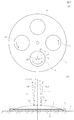
- FIG. 2 the positions of the incident points P1, P2 and P3 to which the laser incident light Ld is irradiated on the surface of the semiconductor layer 7 and the incidents of the laser incident lights Ld1, Ld2 and Ld3 toward the incident points P1, P2 and P3.
- the direction as well as the direction of reflection of the laser reflected light Lv1, Lv2, Lv3 are shown.
- the source gas 5 is introduced into the chamber 2 in a state in which the table 3 and the substrate 6 are heated by the heater 3 a, and the semiconductor layer 7 grows on the surface of the transparent substrate 6.
- the semiconductor layer 7 formed on the surface of the substrate 6 is for forming a molecular layer of a light emitting diode or other semiconductor element, and is, for example, AlN, GaAs, GaN, InP, Si, or SiC.
- a plurality of substrates 6 are mounted on the table 3.
- the table 3 is driven by a motor and can rotate counterclockwise.
- each substrate 6 is driven by a motor and can be individually rotated counterclockwise on the table 3.
- the light emission timing of the laser light L0 in the light emitting device 11 is controlled by the laser light emission control unit 15, and the reflection surface of the pivot mirror 12 is synchronized by the mirror drive control unit 16.
- the orientation of 12c is controlled.
- the control operation is performed at high speed continuously or intermittently, and the laser light L0 is sequentially irradiated to different irradiation points on the surface of the film according to the change in the direction of the reflection surface 12c.
- the laser incident light Ld2 and the laser incident light Ld3 irradiated toward the incident point P3 are continuously converted into substantially three laser incident lights.
- the laser incident lights Ld1, Ld2 and Ld3 may be irradiated once on the surface of the semiconductor layer 7, or may be irradiated in a plurality of cycles in the order of Ld1 ⁇ Ld1 ⁇ Ld3.
- the neutral position of the pivot mirror 12 is determined, a predetermined point (F in FIG. 2) of the film surface is determined, and laser incident light is given in the vicinity of the predetermined point F.
- the predetermined point is a target point that determines the irradiation area of the plurality of irradiation points P1, P2, and P3. The laser light is not given to the predetermined point F.
- FIG. 2B is a side view of the substrate 6 and the semiconductor layer 7 shown in FIG. 2A as viewed from the side.
- the periphery of the circular substrate 6 is held by a ring-shaped holding jig 25 and fixed on the table 3.
- FIG. 2 (b) a state is shown in which warpage in which the laminate of the substrate 6 and the semiconductor layer 7 is convex upward is generated.
- substantially three laser incident lights Ld1, Ld2 and Ld3 whose incident direction is changed continuously or intermittently by the pivot mirror 12 with the substrate 6 stopped without rotating are semiconductor layers.
- the light is irradiated to three incident points P1, P2 and P3 on the surface of.
- the laser incident light Ld1 is reflected at the incident point P1 to become the laser reflected light Lv1.
- the laser incident light Ld2 is reflected at the incident point P2 to become the laser reflected light Lv2
- the laser incident light Ld3 is irradiated at the incident point P3 to become the laser reflected light Lv3.
- the tilt angle can be known on the surface of the semiconductor layer 7 at the incident point P1.
- the inclination angle of the surface of the semiconductor layer 7 at the incident points P2 and P3 can be known by measuring the change in the angle of the reflection direction of the laser reflected light Lv2 and Lv3 with respect to the incident direction of the laser incident light Ld2 and Ld3. it can.
- the irradiation direction of the laser incident light is three directions, and the laser incident light is irradiated to the three incident points P1, P2 and P3 so that the substrate 6 is stopped or only rotating. Even if the top of the warpage is located directly below the first window 8 and the predetermined point F is the top of the warpage, the curvature of the warpage can be measured. Furthermore, the shape change of the surface of the semiconductor layer 7 can be related by setting, preferably, three incident points at at least two incident points on the surface of the semiconductor layer 7 formed on the substrate 6 which revolves while rotating. The amount of information increases, and it is possible to analyze the surface shape of the film in detail.
- FIGS. 3A and 3B show the principle of measuring the surface shape of the semiconductor layer 7 by the measuring device 10.
- the beam splitter 13 is not provided, the pivot mirror 12 faces the outside of the first window 8 of the chamber 2, and the optical position sensor 14 is outside the second window 9.
- the measurement principle is explained on the basis of the arranged structure. The measurement principle is the same as in the measurement apparatus 10A having the beam splitter 13, as shown in FIG.
- FIG. 3A schematically shows a configuration as viewed from obliquely above the semiconductor layer 7.
- the semiconductor layer 7 during or after film formation on the substrate 6 is assumed to be rotationally moved in the direction indicated by the white arrow.
- the laser emission control unit 15 and the mirror drive control unit 16 By operating the laser emission control unit 15 and the mirror drive control unit 16 in synchronization at high speed, the irradiation directions of the laser incident lights Ld1, Ld2 and Ld3 are switched at high speed, and three incident points on the surface of the semiconductor layer 7 are obtained.
- the laser light is switched at high speed and sequentially irradiated. Assuming that the incident points to which the laser incident lights Ld1, Ld2 and Ld3 are irradiated at a certain point are P1, P2 and P3 shown in FIG. 3A, the laser reflected light Lv1 reflected at the incident point P1 is Light is received at the light receiving point R1 of the light position sensor 14.
- the laser reflected light Lv2 reflected at the incident point P2 is received at the light receiving point R2 of the light position sensor 14, and the laser reflected light Lv3 reflected at the incident point P3 is received at the light received point R3 of the light position sensor 14. Light is received.
- the light position sensor 14 Since the light position sensor 14 receives the laser reflected lights Lv1, Lv2, Lv3 in order at different times, the light reception point R1, R2, R3 is detected by adjusting the acquisition timing of data in the light position sensor 14. The position can be detected individually. The detection output is provided to the reflected light analysis unit 17.
- FIG. 3B shows a state in which the laser incident light Ld2 is given to the incident point P2 on the surface of the semiconductor layer 7, and the laser reflected light Lv2 is detected at the light receiving point R2 of the light position sensor 14.
- the deflection angle of the laser incident light Ld at this time is ⁇ .
- the position Le indicates the height level of the incident point P2 on the surface of the semiconductor layer 7.
- D1 indicates the distance in the height direction from the incident point M0 of the laser beam L0 to the pivot mirror 12 to the position Le.
- D2 represents the height distance from the light receiving point R2 at the light position sensor 14 to the position Le
- D3 represents the distance between the incident point M0 of the laser beam L0 to the pivot mirror 12 and the light receiving point R2 at the light position sensor 14 It shows the distance in the horizontal direction.
- the central control unit 20 From the information on the polarization angle ⁇ and the information on the distances D1, D2 and D3 shown in FIG. 3B, the central control unit 20 knows the angle of the surface of the semiconductor layer 7 at the incident point P2. Can. Similarly at the incident points P1 and P3, the angle of the surface of the semiconductor layer 7 can be known, and the curvature of warpage of the region including the incident points P1, P2 and P3 can be calculated.
- the three incident points change from P1 ′, P2 ′, P3 ′ to P1 ′ ′, P2 ′ ′, P3 ′ ′
- the mirror drive control unit 16 controls the operation of the drive units 12a and 12b, and the polarization of the laser incident light Ld1, Ld2 and Ld3 reflected by the pivot mirror 12
- the angle ( ⁇ shown in FIG. 3B) can be changed to change the relative angle of the incident direction of the three laser incident lights Ld1, Ld2 and Ld3.
- the relative positions of the incident points P1, P2, and P3 on the surface of the semiconductor layer 7, that is, the distances from the predetermined point F to the incident points P1, P2, and P3 can be changed.
- the incident points P1, P2 and P3 are preferably located at the respective apexes of an equilateral triangle, assuming that the plane to which the laser light is given is a horizontal plane.
- the size of the triangle can be changed while maintaining the similarity.
- the size of the triangle may be changed and may be changed to a triangle other than an equilateral triangle.
- the positions of the incident points to which the three laser incident lights Ld1, Ld2 and Ld3 are irradiated are P1, P2 and P3 to P1 '. , P2 'and P3', and further to P1 '', P2 '' and P3 ''.
- the size of the triangle in which the three incident points are located at the apex is larger than that formed by P1, P2 and P3 by P1 ′, P2 ′ and P3 ′, and further, P1 ′ ', P2 ′ ′ and P3 ′ ′ are the smallest.
- the relative angles of the incident directions of the three laser incident lights Ld1, Ld2, and Ld3 are changed, and the positions of the incident points P1, P2, and P3, that is, the intervals between the respective incident points are changed.
- An appropriate measurement can be made according to the curvature of the surface of the film being measured. For example, when it is determined that the curvature of the surface of the film being detected is smaller than a predetermined value (when it is close to a plane), the central control unit 20 sets the distance between the incident points P1, P2, and P3 to By spreading, the radius of curvature can be measured with high accuracy.
- the mirror drive control unit 16 controls the drive units 12a and 12b, and the relative angle of the incident direction of the laser incident light Ld1, Ld2 and Ld3 directed from the pivot mirror 12 to the film surface It is possible to change the polarization angles (incident angles) of all the laser incident lights Ld1, Ld2, Ld3 without changing.
- the predetermined points F set at the centers of the incident points P1, P2, P3 and the pivot mirror 12 without changing the shape and size of the triangle in which the incident points P1, P2, P3 are located at the apexes
- the incident direction to the film of the virtual center line connecting the incident point M0 of the laser beam L0 can be changed.
- FIG. 5 it is assumed that the substrate 6 and the semiconductor layer 7 move in the direction of the white arrow.
- the position of the pivot mirror facing the semiconductor layer 7 at a certain point is indicated by reference numeral 12A, and the position of the optical position sensor is indicated by 14A, and the pivot facing the semiconductor layer 7 after the semiconductor layer 7 has moved a predetermined distance.
- the position of the mirror is indicated by 12B and the position of the light position sensor is indicated by 14B.
- the average polarization angle of the laser incident lights Ld1, Ld2, Ld3 (the imaginary center line connecting the incident point M0 and the predetermined point F)
- an average polarization angle of the laser incident light Ld1, Ld2 and Ld3 (a virtual connecting the incident point M0 and the predetermined point F ' The polarization angle of the center line) is ⁇ 2.
- the curvature and inclination angle of the film surface during film formation differ from place to place, and the inclination direction of the surface of the film on which the incident points P1, P2 and P3 are set always changes.
- all the laser reflected lights Lv1, Lv2, Lv3 can not pass through the second window 9, or all the laser reflected lights Lv1, Lv2, Lv3 can not be received by the light position sensor 14. is there.
- the light position sensor 14 can be controlled to receive all the laser reflected lights Lv1, Lv2, Lv3.
- FIG. 6 shows a more specific embodiment showing the method and apparatus for measuring the surface shape of the present invention.
- the laser beam L0 emitted from the light emitting device 11 is reflected by the pivot mirror 12 and the second mirror 113, and the glass is fitted into the beam splitter 13 and the first window 8.
- the light passes through the transparent plate 8A such as a plate and is applied to the surface of the semiconductor layer 7 in the chamber 2.
- the pivot mirror 12 which is the first mirror, is driven by the drive units 12a and 12b shown in FIG. 1, and the direction of the laser beam L0 is changed by the operation of the pivot mirror 12, and three laser beams are incident.
- Light Ld1, Ld2 and Ld3 are incident on the film.
- the second mirror 113 changes the direction in which each of the three laser incident lights Ld1, Ld2 and Ld3 is directed to the surface of the film. That is, the second mirror 113 changes the incident direction to the predetermined point F set on the surface of the film.
- the operation of the pivot mirror 12 only needs to convert the direction of the laser beam L0 into the direction of the three laser incident lights Ld1, Ld2 and Ld3. Control can be simplified.
- the direction of the second mirror 113 may be manually changed or controlled to always change the direction of the second mirror 113 using an electromagnetic drive device having a coil and a magnet or the like. You can also.
- the pivot mirror 12 operates at a high speed to change the laser beam L0 continuously or intermittently to the three laser incident beams Ld1, Ld2, Ld3, and the second mirror 113 is a film of It will operate at relatively slow speeds to accommodate changes in surface orientation.
- a light absorbing member 114 is provided to prevent further reflection of the reflected component of the laser incident light Ld which can not be transmitted through the beam splitter 13, and a light component returned from the chamber 2 and whose direction can be changed by the transparent plate 8A.
- a light absorbing member 115 is provided to prevent reflection of light.
- the light absorbing members 114 and 115 are formed in a light absorbing color such as black, or configured to have a diffuse reflection surface that diffusely reflects light.
- the measuring apparatus 10A of the above embodiment changes the emission timing of the laser beam L0 and the direction of the reflecting surface 12c of the pivot mirror 12 to further add one, two, or four or more laser incident lights.
- the optimum shape measurement can be realized according to the type of film to be measured or according to the shape.
- the return position of the laser reflected light Lv is expanded, it is also possible to arrange a plurality of light position sensors 14 side by side.
Landscapes
- Physics & Mathematics (AREA)
- General Physics & Mathematics (AREA)
- Optics & Photonics (AREA)
- Length Measuring Devices By Optical Means (AREA)
- Testing Or Measuring Of Semiconductors Or The Like (AREA)
Abstract
Description
ミラーの角度を連続的または間欠的に高速に変化させ、前記ミラーによって、単一のレーザー光を、その入射方向を変えながら膜の表面の所定点の回りの複数の照射点に与え、レーザー光の反射方向を光位置センサで検知し、その検知情報から前記所定点での表面の反りを測定することを特徴とするものである。
本発明の表面形状の測定方法は、前記照射点を3か所以上に設定することが好ましい。
単一のレーザー光を与える発光装置と、前記レーザー光を前記膜の表面に向けて反射するミラーと、前記ミラーの反射方向を変化させる駆動部とが設けられ、前記ミラーの角度を連続的または間欠的に高速に変化させ、前記ミラーによって、単一のレーザー光が、その入射方向を変えながら膜の表面の所定点の回りの複数の照射点に与えられ、
ぞれぞれの前記入射点から反射されるレーザー光の光路上に配置された光位置センサが設けられ、レーザー光の反射方向が前記光位置センサで検知され、その検知情報から前記所定点での表面の反りが測定されることを特徴とするものである。
2 チャンバ
3 テーブル
6 基板
7 半導体層
8 第1の窓
9 第2の窓
10A 測定装置
10B 回路構成部
11 発光装置
12 ピボットミラー(第1のミラー)
12a、12b 駆動部
13 ビームスプリッタ
14 光位置センサ
15 レーザー発光制御部
16 ミラー駆動制御部
17 反射光分析部
20 中央制御装置
21 材料ガス制御部
113 第2のミラー
Ld1,Ld2,Ld3 レーザー入射光
Lv1,Lv2,Lv3 レーザー反射光
P1,P2,P3 入射点
Claims (10)
- チャンバ内で基板の表面に成長する膜の表面形状を測定する方法において、
ミラーの角度を連続的または間欠的に高速に変化させ、前記ミラーによって、単一のレーザー光を 、その入射方向を変えながら膜の表面の所定点の回りの複数の照射点に与え、レーザー光の反射方向を光位置センサで検知し、その検知情報から、前記所定点での表面の反りを測定することを特徴とする表面形状の測定方法。 - 複数の前記照射点から反射されるレーザー光から、それぞれの照射点での前記表面の傾きを検知し、その傾きから前記反りを測定する請求項1記載の表面形状の測定方法。
- 前記レーザー光の照射タイミングと、前記ミラーの反射角度とを、高速に制御することで、膜の表面へのレーザー光の入射方向を変化させる請求項1または2記載の表面形状の測定方法。
- 前記ミラーの角度を制御することで、それぞれの照射点に与えられるレーザー光の入射方向の相対角度を変化させる請求項1ないし3のいずれかに記載の表面形状の測定方法。
- 測定された膜の表面の反りに応じて前記相対角度を変化させる請求項4記載の表面形状の測定方法。
- 前記ミラーの角度を制御することで、前記所定点へ向かう入射角度を変化させ、複数の前記照射点から反射された全ての前記レーザー光を前記光位置センサで受光できるようする請求項1ないし5のいずれかに記載の表面形状の測定方法。
- レーザー光を2つのミラーで膜の表面に向け、第1のミラーで、前記所定点の回りの複数の照射点にレーザー光与え、第2のミラーで、前記所定点へ向かう入射角度を変化させる請求項6記載の表面形状の測定方法。
- 前記照射点を3か所以上に設定する請求項1ないし7のいずれかに記載の表面形状の測定方法。
- チャンバ内で基板の表面に成長する膜の表面形状を測定する測定装置において、
単一のレーザー光を与える発光装置と、前記レーザー光を前記膜の表面に向けて反射するミラーと、前記ミラーの反射方向を変化させる駆動部とが設けられ、前記ミラーの角度を連続的または間欠的に高速に変化させ、前記ミラーによって、単一のレーザー光が、その入射方向を変えながら膜の表面の所定点の回りの複数の照射点に与えられ、
ぞれぞれの前記入射点から反射されるレーザー光の光路上に配置された光位置センサが設けられ、レーザー光の反射方向が前記光位置センサで検知され、その検知情報から前記所定点での表面の反りが測定されることを特徴とする表面形状の測定装置。 - 前記発光装置と前記ミラーがチャンバの外に設けられて、前記レーザー光が、前記チャンバに設けられた窓を透過して前記チャンバの内部へ与えられ、反射されたレーザー光が同じくチャンバに設けられた窓を透過して、前記チャンバの外に設けられた前記光位置センサで検知される請求項9記載の表面形状の測定装置。
Priority Applications (7)
| Application Number | Priority Date | Filing Date | Title |
|---|---|---|---|
| EP14898549.2A EP3176539B1 (en) | 2014-07-30 | 2014-07-30 | Device for measuring and method for measuring surface shape |
| US15/329,548 US10283419B2 (en) | 2014-07-30 | 2014-07-30 | Method and apparatus for measuring surface profile |
| CA2956518A CA2956518C (en) | 2014-07-30 | 2014-07-30 | Method and apparatus for measuring surface profile |
| PCT/JP2014/070114 WO2016016972A1 (ja) | 2014-07-30 | 2014-07-30 | 表面形状の測定方法および測定装置 |
| KR1020177005515A KR102225232B1 (ko) | 2014-07-30 | 2014-07-30 | 표면 형상의 측정방법 및 측정장치 |
| CN201480081978.3A CN106716056B (zh) | 2014-07-30 | 2014-07-30 | 表面形状的测量方法以及测量装置 |
| JP2016537660A JP6464513B2 (ja) | 2014-07-30 | 2014-07-30 | 表面形状の測定方法および測定装置 |
Applications Claiming Priority (1)
| Application Number | Priority Date | Filing Date | Title |
|---|---|---|---|
| PCT/JP2014/070114 WO2016016972A1 (ja) | 2014-07-30 | 2014-07-30 | 表面形状の測定方法および測定装置 |
Publications (1)
| Publication Number | Publication Date |
|---|---|
| WO2016016972A1 true WO2016016972A1 (ja) | 2016-02-04 |
Family
ID=55216915
Family Applications (1)
| Application Number | Title | Priority Date | Filing Date |
|---|---|---|---|
| PCT/JP2014/070114 Ceased WO2016016972A1 (ja) | 2014-07-30 | 2014-07-30 | 表面形状の測定方法および測定装置 |
Country Status (7)
| Country | Link |
|---|---|
| US (1) | US10283419B2 (ja) |
| EP (1) | EP3176539B1 (ja) |
| JP (1) | JP6464513B2 (ja) |
| KR (1) | KR102225232B1 (ja) |
| CN (1) | CN106716056B (ja) |
| CA (1) | CA2956518C (ja) |
| WO (1) | WO2016016972A1 (ja) |
Cited By (4)
| Publication number | Priority date | Publication date | Assignee | Title |
|---|---|---|---|---|
| WO2017173129A1 (en) * | 2016-03-30 | 2017-10-05 | Applied Materials, Inc. | Metrology system for substrate deformation measurement |
| US10283419B2 (en) | 2014-07-30 | 2019-05-07 | Ysystems, Ltd. | Method and apparatus for measuring surface profile |
| WO2019180899A1 (ja) * | 2018-03-23 | 2019-09-26 | 株式会社日立ハイテクノロジーズ | 外観検査装置 |
| JP2021507240A (ja) * | 2017-12-21 | 2021-02-22 | エピガン ナムローゼ フェンノートシャップ | ウエハの表面の曲率決定システム |
Families Citing this family (9)
| Publication number | Priority date | Publication date | Assignee | Title |
|---|---|---|---|---|
| CN105091788B (zh) * | 2014-05-06 | 2017-11-07 | 北京智朗芯光科技有限公司 | 自动实时快速检测晶片基底二维形貌的装置 |
| KR101966813B1 (ko) * | 2017-06-09 | 2019-04-08 | 세메스 주식회사 | 측정 장치 및 측정 방법 |
| JP2020047617A (ja) * | 2018-09-14 | 2020-03-26 | キオクシア株式会社 | 基板処理装置、半導体装置の製造方法、および被加工基板 |
| CN111208144B (zh) * | 2020-03-05 | 2022-11-22 | 上海御微半导体技术有限公司 | 一种缺陷检测系统和缺陷检测方法 |
| CN112539698B (zh) * | 2020-11-09 | 2021-12-31 | 北京工业大学 | 一种激光光束作用材料内部在线跟踪与实时反馈的方法 |
| CN114061477B (zh) * | 2021-11-19 | 2022-09-23 | 楚赟精工科技(上海)有限公司 | 翘曲测量方法、翘曲测量装置及成膜系统 |
| US20240248298A1 (en) * | 2023-01-25 | 2024-07-25 | Applied Materials, Inc. | Apparatus and methods for heating tunability in processing chambers |
| US20240248297A1 (en) * | 2023-01-25 | 2024-07-25 | Applied Materials, Inc. | Apparatus and methods for heating tunability in processing chambers |
| CN118670299B (zh) * | 2024-08-20 | 2024-12-06 | 中微半导体(上海)有限公司 | 一种在线测量晶圆曲率的测量系统和测量方法 |
Citations (6)
| Publication number | Priority date | Publication date | Assignee | Title |
|---|---|---|---|---|
| JPH0626842A (ja) * | 1991-09-20 | 1994-02-04 | Hitachi Ltd | 一次元走査型表面変位計 |
| JPH07234116A (ja) * | 1994-02-24 | 1995-09-05 | Nippon Steel Corp | 板材の反り量測定方法 |
| JPH0845922A (ja) * | 1994-07-29 | 1996-02-16 | Fujitsu Ltd | ウェーハ処理方法およびウェーハ処理装置 |
| JPH09126913A (ja) * | 1995-10-30 | 1997-05-16 | Hitachi Ltd | 応力測定装置および半導体製造装置 |
| US5912738A (en) * | 1996-11-25 | 1999-06-15 | Sandia Corporation | Measurement of the curvature of a surface using parallel light beams |
| US20080186512A1 (en) * | 2005-08-01 | 2008-08-07 | Bong Kee | Apparatus and Method for Measuring Curvature Using Multiple Beams |
Family Cites Families (18)
| Publication number | Priority date | Publication date | Assignee | Title |
|---|---|---|---|---|
| JPS5593008A (en) * | 1979-01-09 | 1980-07-15 | Canon Inc | Signal formation unit |
| US4494874A (en) * | 1981-07-07 | 1985-01-22 | Robotic Vision Systems, Inc. | Detection of three-dimensional information using a projected point or line of light |
| US4452534A (en) * | 1981-09-01 | 1984-06-05 | Gribanov Dmitry D | Method of determining geometric parameters of object's surface and device therefor |
| GB8606748D0 (en) * | 1986-03-19 | 1986-04-23 | Secr Defence | Monitoring surface layer growth |
| CN1214232C (zh) * | 2003-03-28 | 2005-08-10 | 中国科学院力学研究所 | 一种自由曲面的测量方法 |
| US7196801B1 (en) * | 2004-02-03 | 2007-03-27 | Kla-Tencor Technologies Corporation | Patterned substrate surface mapping |
| US7570368B2 (en) * | 2004-05-12 | 2009-08-04 | Veeco Instruments Inc. | Method and apparatus for measuring the curvature of reflective surfaces |
| US7505150B2 (en) * | 2005-05-13 | 2009-03-17 | Laytec Gmbh | Device and method for the measurement of the curvature of a surface |
| GB0614423D0 (en) * | 2006-07-20 | 2006-08-30 | Rolls Royce Plc | Method for characterising the profile of a surface |
| GB0706288D0 (en) * | 2007-03-30 | 2007-05-09 | Nightingale Eos Ltd | Method for measuring the thickness or curvature of thin films |
| EP2299236B1 (en) * | 2009-09-17 | 2013-04-10 | LayTec Aktiengesellschaft | Method and apparatus for real-time determination of curvature and azimuthal asymmetry of a surface |
| WO2012099151A1 (ja) | 2011-01-18 | 2012-07-26 | オリンパス株式会社 | 光走査装置および走査型検査装置 |
| KR20130103060A (ko) * | 2012-03-09 | 2013-09-23 | 삼성전기주식회사 | 3차원 측정 장치 및 방법 |
| JPWO2014016995A1 (ja) * | 2012-07-26 | 2016-07-07 | 日本電気株式会社 | 三次元物体計測装置、三次元物体計測装置制御プログラム、三次元物体計測装置制御方法 |
| CN106716056B (zh) | 2014-07-30 | 2020-01-31 | 瓦伊系统有限公司 | 表面形状的测量方法以及测量装置 |
| JP6272743B2 (ja) * | 2014-09-24 | 2018-01-31 | 株式会社ニューフレアテクノロジー | 基板処理装置 |
| US9551569B2 (en) * | 2014-10-13 | 2017-01-24 | Hermes-Epitek Corporation | Apparatus and method for curvature and thin film stress measurement |
| TWI506242B (zh) * | 2014-12-12 | 2015-11-01 | Ind Tech Res Inst | 薄膜曲率量測裝置及其方法 |
-
2014
- 2014-07-30 CN CN201480081978.3A patent/CN106716056B/zh not_active Expired - Fee Related
- 2014-07-30 US US15/329,548 patent/US10283419B2/en active Active
- 2014-07-30 EP EP14898549.2A patent/EP3176539B1/en active Active
- 2014-07-30 WO PCT/JP2014/070114 patent/WO2016016972A1/ja not_active Ceased
- 2014-07-30 JP JP2016537660A patent/JP6464513B2/ja active Active
- 2014-07-30 CA CA2956518A patent/CA2956518C/en active Active
- 2014-07-30 KR KR1020177005515A patent/KR102225232B1/ko active Active
Patent Citations (6)
| Publication number | Priority date | Publication date | Assignee | Title |
|---|---|---|---|---|
| JPH0626842A (ja) * | 1991-09-20 | 1994-02-04 | Hitachi Ltd | 一次元走査型表面変位計 |
| JPH07234116A (ja) * | 1994-02-24 | 1995-09-05 | Nippon Steel Corp | 板材の反り量測定方法 |
| JPH0845922A (ja) * | 1994-07-29 | 1996-02-16 | Fujitsu Ltd | ウェーハ処理方法およびウェーハ処理装置 |
| JPH09126913A (ja) * | 1995-10-30 | 1997-05-16 | Hitachi Ltd | 応力測定装置および半導体製造装置 |
| US5912738A (en) * | 1996-11-25 | 1999-06-15 | Sandia Corporation | Measurement of the curvature of a surface using parallel light beams |
| US20080186512A1 (en) * | 2005-08-01 | 2008-08-07 | Bong Kee | Apparatus and Method for Measuring Curvature Using Multiple Beams |
Non-Patent Citations (1)
| Title |
|---|
| See also references of EP3176539A4 * |
Cited By (7)
| Publication number | Priority date | Publication date | Assignee | Title |
|---|---|---|---|---|
| US10283419B2 (en) | 2014-07-30 | 2019-05-07 | Ysystems, Ltd. | Method and apparatus for measuring surface profile |
| WO2017173129A1 (en) * | 2016-03-30 | 2017-10-05 | Applied Materials, Inc. | Metrology system for substrate deformation measurement |
| CN109075093A (zh) * | 2016-03-30 | 2018-12-21 | 应用材料公司 | 用于基板变形测量的计量系统 |
| US10923371B2 (en) | 2016-03-30 | 2021-02-16 | Applied Materials, Inc. | Metrology system for substrate deformation measurement |
| JP2021507240A (ja) * | 2017-12-21 | 2021-02-22 | エピガン ナムローゼ フェンノートシャップ | ウエハの表面の曲率決定システム |
| JP7185693B2 (ja) | 2017-12-21 | 2022-12-07 | ソイテック ベルジャム ナムローゼ フェンノートシャップ | ウエハの表面の曲率決定システム |
| WO2019180899A1 (ja) * | 2018-03-23 | 2019-09-26 | 株式会社日立ハイテクノロジーズ | 外観検査装置 |
Also Published As
| Publication number | Publication date |
|---|---|
| CA2956518A1 (en) | 2016-02-04 |
| US10283419B2 (en) | 2019-05-07 |
| US20170221776A1 (en) | 2017-08-03 |
| KR102225232B1 (ko) | 2021-03-08 |
| CN106716056A (zh) | 2017-05-24 |
| EP3176539A4 (en) | 2018-03-07 |
| EP3176539A1 (en) | 2017-06-07 |
| KR20170039248A (ko) | 2017-04-10 |
| CN106716056B (zh) | 2020-01-31 |
| EP3176539B1 (en) | 2020-01-01 |
| CA2956518C (en) | 2021-03-30 |
| JP6464513B2 (ja) | 2019-02-06 |
| JPWO2016016972A1 (ja) | 2017-06-01 |
Similar Documents
| Publication | Publication Date | Title |
|---|---|---|
| JP6464513B2 (ja) | 表面形状の測定方法および測定装置 | |
| EP1771599B1 (en) | Epitaxial reactor with susceptor controlled positioning | |
| KR101682914B1 (ko) | 곡률 측정 장치 및 곡률 측정 방법 | |
| KR102500123B1 (ko) | 웨이퍼 표면 곡률 결정 시스템 | |
| TWI668435B (zh) | 光學測量裝置及光學測量方法 | |
| EP2299236A1 (en) | Method and apparatus for real-time determination of curvature and azimuthal asymmetry of a surface | |
| JP4681607B2 (ja) | 回転デバイス上の半導体基板の位置検出装置及び方法 | |
| KR20220157466A (ko) | Epi 챔버를 위한 인-시튜 온도 매핑 | |
| TW202125602A (zh) | 檢測裝置 | |
| US20180223434A1 (en) | Vapor growth apparatus, and vapor growth method | |
| CN207043571U (zh) | 激光划线设备 | |
| JP5184431B2 (ja) | Mocvd装置 | |
| KR20250092254A (ko) | 실시간 프로세스 제어를 위한 인-시튜 반사측정 | |
| TWI632341B (zh) | 曲率測量裝置以及曲率測量方法 | |
| JP2021118361A (ja) | 反り測定装置、気相成長装置および反り測定方法 | |
| JP2006189261A (ja) | 半導体基板の温度測定装置及びその利用 | |
| JP6172672B2 (ja) | 気相成長装置の膜厚測定方法 | |
| CN116031125A (zh) | 一种离子植入机及晶圆固定板的角度确定方法 | |
| JP4893414B2 (ja) | 載置台整準方法及び載置台整準装置 | |
| JP2016180627A (ja) | 偏光光測定装置、および偏光光照射装置 | |
| CN116008234B (zh) | 一种反射率光学测量装置 | |
| JPH0666515B2 (ja) | レ−ザダイオ−ドチツプの位置調整装置 | |
| JPH03285326A (ja) | 光学窓の姿勢制御方法 | |
| KR20070040797A (ko) | 위치결정 제어를 받는 서셉터를 가진 적층 리액터 | |
| JP2015064307A (ja) | 姿勢調整装置、エリプソメータおよび光学条件取得方法 |
Legal Events
| Date | Code | Title | Description |
|---|---|---|---|
| 121 | Ep: the epo has been informed by wipo that ep was designated in this application |
Ref document number: 14898549 Country of ref document: EP Kind code of ref document: A1 |
|
| ENP | Entry into the national phase |
Ref document number: 2016537660 Country of ref document: JP Kind code of ref document: A |
|
| REEP | Request for entry into the european phase |
Ref document number: 2014898549 Country of ref document: EP |
|
| WWE | Wipo information: entry into national phase |
Ref document number: 2014898549 Country of ref document: EP |
|
| WWE | Wipo information: entry into national phase |
Ref document number: 15329548 Country of ref document: US |
|
| ENP | Entry into the national phase |
Ref document number: 2956518 Country of ref document: CA |
|
| NENP | Non-entry into the national phase |
Ref country code: DE |
|
| ENP | Entry into the national phase |
Ref document number: 20177005515 Country of ref document: KR Kind code of ref document: A |