WO2016060206A1 - 光受信器、アクティブ光ケーブル、及び、光受信器の制御方法 - Google Patents
光受信器、アクティブ光ケーブル、及び、光受信器の制御方法 Download PDFInfo
- Publication number
- WO2016060206A1 WO2016060206A1 PCT/JP2015/079191 JP2015079191W WO2016060206A1 WO 2016060206 A1 WO2016060206 A1 WO 2016060206A1 JP 2015079191 W JP2015079191 W JP 2015079191W WO 2016060206 A1 WO2016060206 A1 WO 2016060206A1
- Authority
- WO
- WIPO (PCT)
- Prior art keywords
- signal
- voltage
- threshold voltage
- optical
- offset
- Prior art date
- Legal status (The legal status is an assumption and is not a legal conclusion. Google has not performed a legal analysis and makes no representation as to the accuracy of the status listed.)
- Ceased
Links
Images





Classifications
-
- H—ELECTRICITY
- H04—ELECTRIC COMMUNICATION TECHNIQUE
- H04B—TRANSMISSION
- H04B10/00—Transmission systems employing electromagnetic waves other than radio-waves, e.g. infrared, visible or ultraviolet light, or employing corpuscular radiation, e.g. quantum communication
- H04B10/60—Receivers
- H04B10/66—Non-coherent receivers, e.g. using direct detection
- H04B10/69—Electrical arrangements in the receiver
- H04B10/697—Arrangements for reducing noise and distortion
-
- G—PHYSICS
- G01—MEASURING; TESTING
- G01J—MEASUREMENT OF INTENSITY, VELOCITY, SPECTRAL CONTENT, POLARISATION, PHASE OR PULSE CHARACTERISTICS OF INFRARED, VISIBLE OR ULTRAVIOLET LIGHT; COLORIMETRY; RADIATION PYROMETRY
- G01J1/00—Photometry, e.g. photographic exposure meter
- G01J1/42—Photometry, e.g. photographic exposure meter using electric radiation detectors
- G01J1/44—Electric circuits
-
- H—ELECTRICITY
- H03—ELECTRONIC CIRCUITRY
- H03F—AMPLIFIERS
- H03F3/00—Amplifiers with only discharge tubes or only semiconductor devices as amplifying elements
- H03F3/04—Amplifiers with only discharge tubes or only semiconductor devices as amplifying elements with semiconductor devices only
- H03F3/08—Amplifiers with only discharge tubes or only semiconductor devices as amplifying elements with semiconductor devices only controlled by light
- H03F3/087—Amplifiers with only discharge tubes or only semiconductor devices as amplifying elements with semiconductor devices only controlled by light with IC amplifier blocks
-
- H—ELECTRICITY
- H03—ELECTRONIC CIRCUITRY
- H03F—AMPLIFIERS
- H03F3/00—Amplifiers with only discharge tubes or only semiconductor devices as amplifying elements
- H03F3/45—Differential amplifiers
- H03F3/45071—Differential amplifiers with semiconductor devices only
- H03F3/45076—Differential amplifiers with semiconductor devices only characterised by the way of implementation of the active amplifying circuit in the differential amplifier
- H03F3/45475—Differential amplifiers with semiconductor devices only characterised by the way of implementation of the active amplifying circuit in the differential amplifier using IC blocks as the active amplifying circuit
-
- H—ELECTRICITY
- H03—ELECTRONIC CIRCUITRY
- H03F—AMPLIFIERS
- H03F3/00—Amplifiers with only discharge tubes or only semiconductor devices as amplifying elements
- H03F3/45—Differential amplifiers
- H03F3/45071—Differential amplifiers with semiconductor devices only
- H03F3/45479—Differential amplifiers with semiconductor devices only characterised by the way of common mode signal rejection
- H03F3/45928—Differential amplifiers with semiconductor devices only characterised by the way of common mode signal rejection using IC blocks as the active amplifying circuit
- H03F3/45968—Differential amplifiers with semiconductor devices only characterised by the way of common mode signal rejection using IC blocks as the active amplifying circuit by offset reduction
-
- H—ELECTRICITY
- H04—ELECTRIC COMMUNICATION TECHNIQUE
- H04B—TRANSMISSION
- H04B10/00—Transmission systems employing electromagnetic waves other than radio-waves, e.g. infrared, visible or ultraviolet light, or employing corpuscular radiation, e.g. quantum communication
- H04B10/60—Receivers
- H04B10/66—Non-coherent receivers, e.g. using direct detection
- H04B10/69—Electrical arrangements in the receiver
-
- H—ELECTRICITY
- H04—ELECTRIC COMMUNICATION TECHNIQUE
- H04B—TRANSMISSION
- H04B10/00—Transmission systems employing electromagnetic waves other than radio-waves, e.g. infrared, visible or ultraviolet light, or employing corpuscular radiation, e.g. quantum communication
- H04B10/60—Receivers
- H04B10/66—Non-coherent receivers, e.g. using direct detection
- H04B10/69—Electrical arrangements in the receiver
- H04B10/695—Arrangements for optimizing the decision element in the receiver, e.g. by using automatic threshold control
-
- G—PHYSICS
- G01—MEASURING; TESTING
- G01J—MEASUREMENT OF INTENSITY, VELOCITY, SPECTRAL CONTENT, POLARISATION, PHASE OR PULSE CHARACTERISTICS OF INFRARED, VISIBLE OR ULTRAVIOLET LIGHT; COLORIMETRY; RADIATION PYROMETRY
- G01J1/00—Photometry, e.g. photographic exposure meter
- G01J1/42—Photometry, e.g. photographic exposure meter using electric radiation detectors
- G01J1/44—Electric circuits
- G01J2001/444—Compensating; Calibrating, e.g. dark current, temperature drift, noise reduction or baseline correction; Adjusting
-
- H—ELECTRICITY
- H03—ELECTRONIC CIRCUITRY
- H03F—AMPLIFIERS
- H03F2200/00—Indexing scheme relating to amplifiers
- H03F2200/375—Circuitry to compensate the offset being present in an amplifier
-
- H—ELECTRICITY
- H03—ELECTRONIC CIRCUITRY
- H03F—AMPLIFIERS
- H03F2200/00—Indexing scheme relating to amplifiers
- H03F2200/405—Indexing scheme relating to amplifiers the output amplifying stage of an amplifier comprising more than three power stages
-
- H—ELECTRICITY
- H03—ELECTRONIC CIRCUITRY
- H03F—AMPLIFIERS
- H03F2200/00—Indexing scheme relating to amplifiers
- H03F2200/453—Controlling being realised by adding a replica circuit or by using one among multiple identical circuits as a replica circuit
-
- H—ELECTRICITY
- H03—ELECTRONIC CIRCUITRY
- H03F—AMPLIFIERS
- H03F2200/00—Indexing scheme relating to amplifiers
- H03F2200/462—Indexing scheme relating to amplifiers the current being sensed
-
- H—ELECTRICITY
- H03—ELECTRONIC CIRCUITRY
- H03F—AMPLIFIERS
- H03F2200/00—Indexing scheme relating to amplifiers
- H03F2200/481—A resistor being used as sensor
-
- H—ELECTRICITY
- H03—ELECTRONIC CIRCUITRY
- H03F—AMPLIFIERS
- H03F2203/00—Indexing scheme relating to amplifiers with only discharge tubes or only semiconductor devices as amplifying elements covered by H03F3/00
- H03F2203/45—Indexing scheme relating to differential amplifiers
- H03F2203/45152—Balancing means being added at the input of a dif amp to reduce the offset of the dif amp
-
- H—ELECTRICITY
- H03—ELECTRONIC CIRCUITRY
- H03F—AMPLIFIERS
- H03F2203/00—Indexing scheme relating to amplifiers with only discharge tubes or only semiconductor devices as amplifying elements covered by H03F3/00
- H03F2203/45—Indexing scheme relating to differential amplifiers
- H03F2203/45212—Indexing scheme relating to differential amplifiers the differential amplifier being designed to have a reduced offset
Definitions
- the present invention relates to an optical receiver that converts a received optical signal into a voltage signal and outputs the voltage signal to the outside.
- the present invention also relates to an active optical cable including such an optical receiver.
- the present invention relates to a method for controlling such an optical receiver.
- the active optical cable is composed of a cable containing an optical fiber and a pair of connectors provided at both ends of the cable.
- One connector functions as an optical transmitter that converts a voltage signal input from the outside (for example, a data center computer) into an optical signal and transmits the optical signal.
- the other connector functions as an optical receiver that converts a received optical signal into a voltage signal and outputs the voltage signal to the outside (for example, storage in a data center).
- Bidirectional communication using an active optical cable can also be realized if both connectors function as an optical transmitter and an optical receiver.
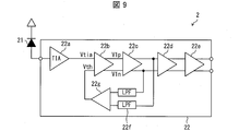
- FIG. 9 shows a conventional optical receiver 2 that can be used as a connector for an active optical cable.
- the optical receiver 2 includes a light receiving element 21 that converts an optical signal into a current signal, and a receiving circuit 22 that converts the current signal into a voltage signal.
- the receiving circuit 22 includes a transimpedance amplifier 22a, differential amplifiers 22b to 22e, a low-pass filter 22f, and an error amplifier 22g.
- the transimpedance amplifier 22a converts the current signal output from the light receiving element 21 into a voltage signal (single end).
- the differential amplifier 22b differentially amplifies the difference between the voltage signal output from the transimpedance amplifier 22a and the threshold voltage Vth to obtain a differential signal composed of a normal phase signal and a negative phase signal.
- the differential amplifier groups 22c to 22e differentially amplify the differential signal output from the differential amplifier 22b.
- the positive phase output voltage V1p of the differential amplifier 22b is expressed by V1ocm + a1 ⁇ (Vtia ⁇ Vth) / 2, and the negative phase output voltage V1n of the differential amplifier 22b is V1ocm. -A1 ⁇ (Vtia ⁇ Vth) / 2.
- V1ocm is the output common mode voltage (predetermined value) of the differential amplifier 22b
- a1 is the gain (predetermined value) of the differential amplifier 22b.
- the differential The waveforms of the normal phase signal and the negative phase signal output from the amplifier 22b are symmetrical with respect to the output common mode voltage V1ocm.
- the waveforms of the normal phase signal and the negative phase signal output from the differential amplifier 22b are as follows: Each becomes asymmetric with respect to the output common mode voltage V1ocm. Due to such asymmetry, the waveform of the output signal of the optical receiver 2 is distorted.
- the low-pass filter 22f and the error amplifier 22g are configured to avoid such a problem.
- the low-pass filter 22f smoothes each of the positive phase signal and the negative phase signal output from the differential amplifier 22c.
- the error amplifier 22g includes a smoothed positive-phase signal (DC component of the positive-phase signal) output from the low-pass filter 22f and a smoothed negative-phase signal (DC of the negative-phase signal) output from the low-pass filter 22f. Component).
- the error amplifier 22g integrates the difference between the values of these two signals, that is, the offset voltage of the differential signal output from the differential amplifier 22c. The integrated value of the offset voltage output from the error amplifier 22g is fed back to the negative phase input of the differential amplifier 22b as the threshold voltage Vth.
- the integrated value of the offset voltage output from the error amplifier 22g follows the average output level of the transimpedance amplifier 22a. For this reason, even if the power of the received optical signal fluctuates, the above problem does not occur.
- Patent Document 1 is an example of a document disclosing a technique for canceling an offset voltage of a differential signal.
- JP 2008-109559 Publication Date: May 8, 2008
- the conventional optical receiver 2 (see FIG. 9) has a problem that the waveform of the output signal is distorted immediately after the optical signal transitions from the non-signal section to the signal section.
- this problem will be described in more detail with reference to FIG.
- FIG. 10A is a waveform diagram of an optical signal received by the light receiving element 21.
- FIG. 10B is a waveform diagram of a voltage signal output from the transimpedance amplifier 22a.
- the time change of the threshold voltage Vth output from the error amplifier 22g is also shown by a dotted line.
- the optical signal shown in FIG. 10A is a pattern composed of a DATA section (signaled section) in which the value alternately takes a high level and a low level, and an IDLE section (no signal section) in which the value continues to take off level. have.
- the transimpedance amplifier 22a When the light receiving element 21 receives the optical signal shown in FIG. 10A, the transimpedance amplifier 22a outputs the voltage signal shown in FIG. 10B.
- the average output level of the transimpedance amplifier 22a differs between the DATA section and the IDLE section. For this reason, the waveform of the output signal of the optical receiver 2 is distorted from the transition from the IDLE section to the DATA section until the output voltage Vth of the error amplifier 22g catches up with the average output level of the transimpedance amplifier 22a in the DATA section. Will occur.
- the present invention has been made in view of the above problems, and an object of the present invention is to provide optical reception capable of performing offset cancellation without distorting the waveform of an output signal immediately after transition from a non-signal section to a signal section. Is to realize the vessel.
- an optical receiver includes a light receiving element that converts an optical signal into a current signal, a transimpedance amplifier that converts the current signal into a voltage signal, the voltage signal, and a threshold voltage.
- a differential amplifier that converts the voltage signal into a differential signal, a no-signal detection circuit that detects a no-signal section of the optical signal, and an offset voltage of the differential signal.
- a controller that repeats an offset canceling process including a threshold voltage changing process for changing the threshold voltage so as to decrease, and the controller skips the threshold voltage changing process in the no-signal interval. It is characterized by.
- a method of controlling an optical receiver includes a light receiving element that converts an optical signal into a current signal, a transimpedance amplifier that converts the current signal into a voltage signal, A differential amplifier that converts the voltage signal to a differential signal by differentially amplifying the difference between the voltage signal and the threshold voltage, and a method for controlling the optical receiver, wherein the optical signal is non-signaled A non-signal detection step of detecting a section, and a control step of repeating an offset cancellation process including a threshold voltage change process of changing the threshold voltage so that the offset voltage of the differential signal becomes small. Is characterized in that the threshold voltage changing process is skipped in the non-signal section of the optical signal.
- the initial value of the variable Vth is set to the maximum value and the minimum value, the received power [dBm] and the change amount [step] of the variable Vth necessary for canceling the offset under the received power
- FIG. 10B is a waveform diagram of a voltage signal output from the transimpedance of the optical receiver illustrated in FIG. 9.
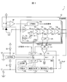
- FIG. 1 is a block diagram showing a configuration of the optical receiver 1.
- the optical receiver 1 is a device that converts a received optical signal into a voltage signal (differential voltage signal in the present embodiment) and outputs it to the outside. As shown in FIG. 1, the optical receiver 1 includes a light receiving element 11, a receiving circuit 12, an MCU (Micro Controller Unit) 13, a nonvolatile memory 14, and a reference voltage source 15.
- MCU Micro Controller Unit
- the light receiving element 11 is configured to convert the received optical signal into a current signal.
- a PD Photo-Diode
- the current signal obtained by the light receiving element 11 is input to the receiving circuit 12.
- the receiving circuit 12 is configured to convert a current signal obtained by the light receiving element 11 into a differential voltage signal (hereinafter referred to as “differential signal”). As shown in FIG. 1, the receiving circuit 12 includes a transimpedance amplifier 12a, a variable voltage source 12b, a dummy transimpedance amplifier 12c, differential amplifiers 12d to 12g, a low-pass filter 12h, a switch 12i, an error amplifier 12j, a LOS (Loss Of Signal) detection circuit 12k and I2C interface 12m.
- the transimpedance amplifier 12a converts the current signal obtained by the light receiving element 11 into a voltage signal (single end).
- the output voltage Vtia of the transimpedance amplifier 12a is input to the negative phase input terminal of the differential amplifier 12d.
- the variable voltage source 12b generates a threshold voltage Vth.
- the magnitude of the threshold voltage Vth generated by the variable voltage source 12b can be controlled from the MCU 13 via the I2C interface 12m.
- the threshold voltage Vth generated by the variable voltage source 12b is input to the positive phase input terminal of the differential amplifier 12d.
- a dummy transimpedance amplifier 12c is interposed between the variable voltage source 12b and the ground. This is for canceling the temperature dependency and power supply voltage dependency of the transimpedance amplifier 12a (voltage components that are included in the output voltage of the transimpedance amplifier 12a and do not depend on the photocurrent Ipd flowing through the light receiving element 11).
- the differential amplifier 12d converts the voltage signal output from the transimpedance amplifier 12a into a differential signal by differentially amplifying the difference between the voltage signal output from the transimpedance amplifier 12a and the threshold voltage Vth.
- the positive phase output voltage V1p of the differential amplifier 12d is expressed by V1ocm + a1 ⁇ (Vtia ⁇ Vth) / 2
- the negative phase output voltage V1n of the differential amplifier 12d is expressed by V1ocm ⁇ a1 ⁇ (Vtia ⁇ Vth) / 2. Is done.
- V1ocm is the output common mode voltage (predetermined value) of the differential amplifier 12d
- a1 is the gain (predetermined value) of the differential amplifier 12d.
- the differential signal obtained by the differential amplifier 12d is input to the differential amplifier groups 12e to 12g.
- the differential amplifier groups 12e to 12g amplify the differential signal obtained by the differential amplifier 12d.
- the differential signals (normal phase output voltage V2p and negative phase output voltage V2n) output from the differential amplifier 12e at the previous stage are input to the low-pass filter 12h. Further, the differential signals (normal phase output voltage V4p and negative phase output voltage V4n) output from the differential amplifier 12g in the subsequent stage are output to the outside of the optical receiver 1.
- the low-pass filter 12h smoothes the normal phase signal and the negative phase signal output from the differential amplifier 12e, respectively.
- the positive phase signal smoothed by the low-pass filter 12h that is, the DC component ⁇ V2p> of the positive phase signal is input to the positive phase input terminal of the error amplifier 12j.
- the anti-phase signal smoothed by the low-pass filter 12h that is, the DC component ⁇ V2n> of the anti-phase signal is input to the anti-phase input terminal of the error amplifier 12j.
- the error amplifier 12j differentially amplifies the difference between the normal phase signal and the negative phase signal smoothed by the low pass filter 12h.
- the sum is expressed as a2 ⁇ ( ⁇ V2p> ⁇ ⁇ V2n>) + Vreff.
- the reference voltage Vref is an output voltage of the reference voltage source 15 connected to the negative input of the error amplifier 12j.
- the output voltage Verr of the error amplifier 12j (hereinafter referred to as “error amplifier output”) Verr is input to the MCU 13.
- the LOS detection circuit 12k is a section in which the value of the received optical signal is off level, that is, a section in which the photocurrent Ipd flowing through the light receiving element 11 is equal to or less than a predetermined threshold (hereinafter referred to as “no-signal section”). Is identified. This threshold value is determined to be, for example, about the same as the magnitude of the dark current flowing through the light receiving element 11 or about the same as the photocurrent flowing through the light receiving element 11 when light emission is received.
- the LOS detection circuit 12k generates a LOS signal indicating the specified no-signal section, and stores the value of the generated LOS signal in a register (not shown).
- a digital signal that takes a value “1” within a no-signal interval and takes a value “0” outside the no-signal interval is used as the LOS signal.
- a clear-on-read register whose value is updated after the value is read is used as a register for storing the value of the LOS signal. Therefore, in the first reading after the end of the no-signal interval, “1” is read as the value of the LOS signal (“0” is read as the value of the LOS signal from the previous reading to the current reading. Only if the non-LOS condition persists). The value of the LOS signal stored in this register is read out to the MCU 13 via the I2C interface 12m.
- a configuration is adopted in which a drop voltage R ⁇ Ipd in a resistor R connected in series with the light receiving element 11 is input to the LOS detection circuit 12k through an operational amplifier OP.
- the LOS detection circuit 12k identifies the no-signal interval by referring to the output voltage of the operational amplifier OP.
- the receiving circuit 12 has the above-described configuration for two or more channels (four channels in this embodiment) except for the error amplifier 12j and the I2C interface 12m.
- the switch 12i switches a channel serving as a signal source of a differential signal input to the error amplifier 12j. That is, the differential signal output from the differential amplifier 12e of the channel selected by the switch 12i is input to the error amplifier 12j.
- the MCU 13 is configured to execute an offset cancellation process, and includes a voltage reading unit 13a, a LOS reading unit 13b, a threshold voltage changing unit 13c, a CH switching unit 13d, and an I2C interface 13e as shown in FIG. Yes.
- the offset cancellation processing is processing for bringing the offset voltage Vos closer to 0 [V] by changing the magnitude of the threshold voltage Vth generated by the variable voltage source 12b, that is, the output voltage of the error amplifier 12j. This refers to the process of bringing Verr close to the reference voltage Vref.
- the flow of the offset cancellation process and the execution timing of the offset cancellation process will be described later with reference to different drawings.
- the nonvolatile memory 14 is configured to store the magnitude of the threshold voltage Vth (more precisely, the value of a variable representing the magnitude of the threshold voltage Vth).
- EEPROM registered trademark
- the MCU 13 executes threshold voltage writing processing for writing the magnitude of the threshold voltage Vth into the nonvolatile memory 14 when the operation of the MCU 13 ends (just before the operation of the MCU 13 ends) such as when the power is turned off. Further, the MCU 13 executes a threshold voltage reading process for reading the magnitude of the threshold voltage Vth from the nonvolatile memory 14 at the start of the operation of the MCU 13 such as when the power is turned on (immediately after the operation of the MCU 13 is started).
- the MCU 13 uses the magnitude of the threshold voltage Vth read from the nonvolatile memory 14 at the start of the operation (written to the nonvolatile memory 14 at the end of the previous operation) as the initial value of the threshold voltage Vth in the offset cancellation process. .
- an alarm generated by a power supply monitoring IC (not shown) when the magnitude of the power supply voltage falls below a predetermined threshold value is processed.
- the start trigger may be used.
- a voltage holding circuit comprising a capacitor C1 and a diode D1 is inserted between the power supply and the MCU 13, and a voltage holding comprising a capacitor C2 and a diode D2 is provided between the power supply and the nonvolatile memory 14. If a circuit is inserted, the MCU 13 and the nonvolatile memory 14 can be normally operated even after the power supply voltage falls below a predetermined threshold value.
- FIG. 2 is a flowchart showing a flow of offset cancel processing executed by the MCU 13.
- the MCU 13 operates as follows.
- Step S11 voltage reading process: The MCU 13 reads the voltage Verr output from the error amplifier 12j and the reference voltage Vref output from the reference voltage source 15 via the A / D converter, and moves the process to step S12.
- the voltage reading unit 13a of the MCU 13 shown in FIG. 1 is configured to execute this voltage reading process.
- Step S12 (LOS reading process): The MCU 13 reads the value of the LOS signal generated by the LOS detection circuit 12k via the I2C interface 13e, and moves the process to step S13.
- the LOS reading unit 13b of the MCU 13 shown in FIG. 1 is configured to execute this LOS reading process.
- Step S13 LOS determination processing: The MCU 13 determines whether or not the value of the LOS signal read by the LOS detection circuit 12k is zero. If the value of the LOS signal is 0, the MCU 13 moves the process to step S14. When the value of the LOS signal is 1, the MCU 13 ends the offset cancellation process.
- Step S14 The MCU 13 changes the magnitude of the threshold voltage Vth generated by the variable voltage source 12b based on the values of the error amplifier output Verr and the reference voltage Vref read by the voltage reading unit 13a, The offset cancel process ends.
- the threshold voltage changing unit 13c of the MCU 13 illustrated in FIG. 1 is configured to execute this threshold voltage changing process.
- the threshold voltage changing unit 13c sets the value of the variable representing the threshold voltage Vth to a value larger by ⁇ than the current value when (1) Verr> Vref + ⁇ holds, and (2) Verr ⁇ Vref ⁇ holds. Sometimes, it is set to a value smaller by ⁇ than the current value.
- ⁇ is a positive constant predetermined as an allowable error.
- the threshold voltage changing unit 13c controls the variable voltage source 12b via the I2C interface 13e so that the magnitude of the threshold voltage Vth matches the set value.
- the flow of the threshold voltage changing process will be described later with reference to another drawing.
- the threshold voltage Vth is smaller than the average level (average value of high level and low level) of the voltage signal output from the transimpedance amplifier 12a. If too large, the threshold voltage Vth is increased by the threshold voltage changing process, and as a result, the value of the offset voltage Vos is decreased.
- Vos ⁇ (equivalent to “Verr ⁇ Vref ⁇ ”)
- the threshold voltage Vth is decreased by the changing process, and as a result, the value of the offset voltage Vos is increased. Therefore, if the above-described offset canceling process is repeated, the absolute value
- the offset cancellation process employs a configuration in which the threshold voltage change process is skipped in the no-signal section. As a result, the waveform of the differential signal is not greatly distorted immediately after the start of the signal period following the no-signal period.
- the above-described offset cancellation process has two execution modes with different speeds for changing the threshold voltage Vth.
- the slower execution mode (second execution mode) for changing the threshold voltage Vth is referred to as “normal control mode”
- the faster execution mode (first execution) for changing the threshold voltage Vth. Mode) is described as “acceleration control mode”.
- the execution mode of the offset cancellation process is set independently for each channel.
- the MCU 13 uses a 1-bit (2-step) binary as a variable representing the execution mode of the offset cancellation process for each channel. Hereinafter, this variable is referred to as “acceleration control flag ACF”. Further, the MCU 13 uses 8-bit binary (256 steps) as a variable representing the threshold voltage Vth. Hereinafter, this variable is referred to as “variable Vth”.
- the MCU 13 determines the execution timing of the offset cancellation process according to the flowchart shown in FIG.
- FIG. 3 is a flowchart showing the overall flow of processing executed by the MCU 13. In each step of the flowchart shown in FIG. 3, the MCU 13 operates as follows.
- Step S101 The MCU 13 initializes the values of the acceleration control flags ACF of all channels to 1. Also, the MCU 13 initializes the value of the main counter n to 1.
- Step S102 The MCU 13 repeats the determination of whether or not the 1 ms timer counter has been counted up until the determination result becomes true. When the determination result is true, the MCU 13 moves the process to step S103.
- Process S103 The MCU 13 determines whether the value of the main counter is 1, 2, 3, or 4. If the determination result is true, the MCU 13 moves the process to step S104. If the determination result is false, the MCU 13 moves the process to step S111.
- Process S104 The MCU 13 determines whether or not the value of the acceleration control flag ACF of the processing target channel is 0. If the determination result is true, the MCU 13 moves the process to step S105. If the determination result is false, the MCU 13 moves the process to step S106.
- Step S105 The MCU 13 initializes the value of the sub-counter m to 1, sets the upper limit value M to 1, and moves the process to step S107.
- Step S106 The MCU 13 initializes the value of the sub-counter m to 1 and sets the upper limit M to 2 and moves the process to step S107.
- Step S107 The MCU 13 executes the offset cancel process shown in FIG. 2 and moves the process to step S108.
- Step S108 The MCU 13 increments the value of the sub-counter m, and moves the process to S109.
- Process S109 The MCU 13 determines whether or not the value of the sub-counter m has reached the upper limit value. If the determination result is true, the MCU 13 moves the process to step S110. If the determination result is false, the MCU 13 returns the process to step S107.
- the CH switching unit 13d of the MCU 13 shown in FIG. 1 has a configuration for executing this Ch switching process. The CH switching unit 13d controls the switch 12i via the I2C interface 13e so that the differential signal output from the differential amplifier 12e of the processing target channel after switching is input to the error amplifier 12j.
- Step S111 The MCU 13 executes other processing (any processing other than the offset cancellation processing), and moves the processing to step S112. This step is provided in order to prevent the offset cancellation process from exclusively using the MCU 13.
- Step S112 The MCU 13 increments the value of the main counter n, and moves the process to step S113.
- Step S113 The MCU 13 determines whether or not the values of the acceleration control flags ACF for all the channels are zero. If the determination result is true, the MCU 13 moves the process to step S114. If the determination result is false, that is, if the value of the acceleration control flag ACF of any channel is 1, the MCU 13 proceeds to step S116.
- Steps S114 to S115 The MCU 13 determines whether or not the value of the main counter n is greater than 100. If the determination result is true, the MCU 13 resets the value of the main counter n to 1, and returns the process to step S102.
- Steps S116 to S117 The MCU 13 determines whether or not the value of the main counter n is greater than 5. If the determination result is true, the MCU 13 resets the value of the main counter n to 1, and returns the process to step S102.
- the execution mode of the offset cancellation process is any one of execution modes 1 to 3 shown in the following table.
- the execution mode of the offset cancellation process is set to the acceleration control mode for all channels (step S101). Therefore, the execution mode of the offset cancellation process for each channel is ⁇ Execution mode 1> in the above table.
- step S104 the execution mode of the offset cancellation process for the channel is ⁇ execution mode 1> in the above table.
- ⁇ execution mode 2> The transition from ⁇ execution mode 1> to ⁇ execution mode 2> occurs independently in each channel.
- the execution mode of the offset cancellation process for each channel is from ⁇ execution mode 2> in the above table. Transition to ⁇ Execution mode 3>.
- the transition from ⁇ execution mode 2> to ⁇ execution mode 3> occurs simultaneously in all channels.
- the execution frequency of the threshold value changing process in ⁇ Effective Mode 3> is set to once / 100 ms, but is not limited to this.
- the execution frequency of the threshold value changing process in ⁇ Effective Mode 3> may be set to once / 5 seconds. In this case, in step S114 described above, it is determined whether or not the value of the main counter n is greater than 5000.
- FIG. 4 shows an operation example of the MCU 13 realized by determining the execution timing of the offset cancellation process according to the flowchart shown in FIG. 4,
- (a) is a waveform diagram showing the waveforms of the optical signal and the LOS signal
- (b) is a diagram showing an operation example of the MCU 13 in the section T1 shown in (a)
- (c) are figures which show one operation example of MCU13 in the section T2 shown to (a)
- (d) is a figure which shows one operation example of MCU13 in the section Tn shown to (a).
- a link for transmitting / receiving a COMINIT signal, a COMSAS signal, a SNT (Speed Negotiation Transmission) signal, and an MTT (Maximum Transmitter Training) signal after power-on is repeated up to 5 times, for example.
- the COMINIT signal, the COMSAS signal, and the SNT signal are OOB signals (an example of “first optical signal” in the claims) in which a DATA section and an IDLE section appear alternately.
- OOB signals have no meaning as signals in the bit pattern of the DATA section, but have meaning as signals in the width (duration) of the DATA section and the IDLE section (for example, the COMSAS signal has a DATA section of 106 ns) It is defined as an OOB signal in which IDLE sections of 960 nsec appear alternately). Therefore, the optical receiver 1 can correctly recognize these OOB signals regardless of whether or not the offset cancellation is completed.
- the MTT signal (an example of “second optical signal” in the claims) is a data signal in which the DATA section continues for 19.9 msec. The MTT signal has no meaning as a signal in the width of the DATA section, and has a meaning as a signal in the bit pattern in the DATA section.
- the LOS signal read by the MCU 13 has a value of 0 in the sections T1, T2,... For receiving the MTT signal and the section Tn for receiving other data signals, as shown in FIG. .
- the threshold voltage changing process is executed in those intervals in which the value of the LOS signal is zero.
- the period at which the MCU 13 reads the LOS signal is longer than the DATA section (106 nsec in the case of the COMSAS signal) of the OOB signal (COMINIT signal, COMSAS signal, and SNT signal), and the DATA section (19.9 ms) of the MTT signal. ) Is set shorter. Therefore, the reading of the LOS signal is executed at most once during the reception of the OOB signal, and is executed at least twice (four times in the present embodiment) during the reception of the MTT signal. Note that the value of the LOS signal read by the MCU 13 does not become 0 in the DATA section of the COMINIT signal, the COMSAS signal, and the SNT signal, as shown in FIG.
- the threshold voltage changing process is not executed in the DATA section of the COMINIT signal, the COMSAS signal, and the SNT signal. Therefore, even if the mark ratios of the COMINIT signal, the COMSAS signal, and the SNT signal are not 50%, there is no concern that the variable Vth is set to an incorrect value during the period in which these signals are received. As long as the mark ratio of the COMINIT signal, the COMSAS signal, and the SNT signal is 50%, the threshold voltage changing process may be executed even in a period in which these signals are received. In this case, it is not necessary to read the value of the LOS signal via the clear-on-read register.
- 4B to 4D are diagrams showing the execution timing of the offset cancel process by arranging a rectangle representing the execution period of the offset cancel process on the time axis for each channel.
- the white rectangle represents an offset cancellation process that does not involve a threshold voltage change process
- the gray (dot hatched) rectangle represents an offset cancel process that involves a threshold voltage change process that changes the value of the variable Vth by one step (0x01).
- the black rectangle represents an offset cancellation process involving a threshold voltage changing process for changing the value of the variable Vth by two steps (0x02).
- FIG. 4 shows a typical operation example of the MCU 13 during a period in which the offset cancellation processing of all channels is executed in the acceleration control mode.
- the offset cancellation process accompanied by the threshold voltage changing process for changing the value of the variable Vth by two steps is executed at a frequency of 2/5 msec in all channels (the above-described case).
- Execution mode 1) in the table is executed immediately after the LOS signal falls. This is because the LOS signal is read out via a clear-on-read register.
- the MCU 13 can execute the threshold voltage changing process a maximum of seven times in each channel, and can change the value of the variable Vth by a maximum of 14 steps (0x0e).
- FIG. 4C shows a typical operation example of the MCU 13 during a period in which a channel in which the offset cancellation process is executed in the acceleration control mode and a channel in which the offset cancellation process is executed in the normal control mode coexist.
- an offset cancellation process involving a threshold voltage changing process for changing the value of the variable Vth by two steps is executed at a frequency of 2/5 msec ( Execution mode 1) in the above table.
- an offset canceling process involving a threshold voltage changing process for changing the value of the variable Vth by two steps is executed at a frequency of 2/5 ms ( Execution mode 1) in the above table
- offset cancellation processing with threshold voltage change processing for changing the value of the variable Vth by one step is executed once every 5 ms in the period from 5 ms to 20 ms after the start (Execution mode 2 in the above table).
- the offset canceling process with the threshold voltage changing process for changing the value of the variable Vth by two steps is executed at a frequency of 2/5 ms ( Execution mode 1)
- an offset cancel process with a threshold voltage change process for changing the value of the variable Vth by one step is executed once every 5 ms.
- FIG. 4C shows a state immediately after the LOS signal has fallen, and the offset cancellation process executed first does not involve a threshold voltage change process.
- FIG. 4 shows a typical operation example of the MCU 13 during a period in which the offset cancellation processing of all channels is executed in the normal control mode.
- the offset cancellation process accompanied by the threshold voltage changing process for changing the threshold voltage Vth value by one step is executed at a frequency of once / 100 ms in all channels (above-mentioned).
- FIG. 4D shows a state immediately after the LOS signal has fallen, and the offset cancel process that is executed first does not involve a threshold voltage change process.
- the light emitting element included in the optical transmitter is a VCSEL
- the reception power varies due to the temperature change of the VCSEL.
- the amount of change in the variable Vth necessary for canceling the offset caused by such power fluctuation (making the absolute value
- the fluctuation range of the power of the optical signal received by the optical receiver 1 (hereinafter referred to as “reception power”) is ⁇ 2.3 dBm / + 2 as an example when the time-dependent deterioration of the VCSEL (details will be described later) is not considered. .6 dBm.
- the initial value of the variable Vth is a value determined so as to cancel the offset under any received power within the fluctuation range.
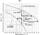
- FIG. 5 shows the received power [dBm] and the amount of change in the variable Vth necessary for canceling the offset under the received power when the initial value of the variable Vth is set to the maximum value and the minimum value. It is the graph obtained by confirming the relationship with [step] experimentally.
- the graph of FIG. 5 shows the following, for example. That is, when the initial value of the variable Vth is set to the maximum value, if the reception power is +1.5 dBm, the offset can be canceled by increasing the value of the variable Vth by 30 steps. Alternatively, when the initial value of the variable Vth is set to the minimum value, if the actual received power is ⁇ 1.5 dBm, the offset can be canceled by decreasing the value of the variable Vth by 10 steps.
- the fluctuation range of the reception power due to the temperature change of the VCSEL is 2.0 dB ( ⁇ 1.5 dB / + 0.5 dB), and a variable necessary for canceling the offset caused by such fluctuation of the reception power.
- the amount of change in Vth is 56 steps or less.
- the offset generated at this time can be canceled by increasing the value of the variable Vth by 50 steps. Also, as shown in FIG.
- the offset generated at this time can be canceled by reducing the value of the variable Vth by 25 steps.
- the power of the optical signal received by the optical receiver 1 (hereinafter referred to as “reception power”) varies due to temperature change and deterioration with time of the VCSEL included in the optical transmitter as a light emitting element.
- the fluctuation range of the reception power due to the temperature change of the VCSEL is about ⁇ 1.5 dB / + 0.5 dB, whereas the fluctuation range of the reception power due to the deterioration of the VCSEL over time is ⁇ 2 dB. / + 0 dB or so.
- the value of the variable Vth expressed as 8-bit binary can be changed by a maximum of 56 steps until the last MTT signal is received. Therefore, even if the received power fluctuates by about 2.0 dB ( ⁇ 1.5 dB / + 0.5 dB) due to the temperature change of the VCSEL, if there is no fluctuation in the received power due to the deterioration of the VCSEL over time, the last link The offset can be canceled reliably before receiving the MTT signal in the up sequence.
- the fluctuation range of the received power is ⁇ 3.5 dB / + 0.5 dB (variation width). 4 dB).
- the amount of change in the variable Vth necessary for canceling the offset caused by such fluctuations in received power exceeds 56 steps.
- the initial value of Vth is set to the maximum value
- the amount of change in the variable Vth necessary for canceling the offset is 80 steps or more. Therefore, if the initial value of the variable Vth is fixed to the factory default value, the offset cannot be canceled before the MTT signal in the last link-up sequence is received.
- the value of the variable Vth at that time is written in the nonvolatile memory 14 at the end of the operation, and the value of the variable Vth read from the nonvolatile memory 14 at the start of the operation is the initial value of the offset cancellation process.
- the structure used as a value is adopted.
- the change amount of the variable Vth necessary for canceling the offset (change amount from the initial value) is ⁇ 1.5 dB / + 0.5 dB (the variation range of the reception power due to the temperature change). It can be suppressed to the extent. For this reason, the offset can be reliably canceled before the MTT signal is received in the last link-up sequence.
- a configuration is employed in which threshold voltage writing processing (processing for writing the value of variable Vth into the nonvolatile memory 14) is executed when the operation of the MCU 13 ends.
- the present invention is not limited to this. is not. That is, for example, a configuration in which the threshold voltage writing process is periodically executed during the operation of the MCU 13 may be employed. By adopting such a configuration, it is not necessary to provide a voltage holding circuit as described above.
- the execution cycle of the threshold voltage writing process is lengthened, the lifetime of the nonvolatile memory 14 is lengthened, but the accuracy as the initial value of the variable Vth stored in a nonvolatile manner is lowered.
- the accuracy as the initial value of the variable Vth stored in a non-volatile manner decreases because the time from when the MCU 13 last executes the threshold voltage writing process until the MCU 13 finishes the operation becomes longer.
- the execution cycle of the threshold voltage writing process is shortened, the lifetime of the nonvolatile memory 14 is shortened, but the accuracy as the initial value of the variable Vth stored in a nonvolatile manner is improved.
- the accuracy as the initial value of the variable Vth stored in a nonvolatile manner is improved because the time from when the MCU 13 last executes the threshold voltage writing process until the MCU 13 finishes the operation is shortened. .
- the threshold voltage write processing execution period is preferably 30 minutes or more and 1 hour 30 minutes or less, preferably 1 hour More preferably.
- FIG. 6 is a flowchart showing the flow of the threshold voltage changing process. In each step of the flowchart shown in FIG. 6, the MCU 13 operates as follows.
- control direction flag CDF is used in addition to the acceleration control flag ACF.
- the control direction flag CDF takes a value of 1 when the direction of control is a direction to increase the value of the variable Vth during acceleration control, and when the direction of control is a direction to decrease the value of the variable Vth during acceleration control.
- Step S201 The MCU 13 determines whether or not the value of the error amplifier output Verr is larger than a value obtained by adding the tolerance ⁇ to the value of the reference voltage Vref. If the determination result is true, the MCU 13 moves the process to step S202. If the determination result is false, the MCU 13 moves the process to step S209.
- Step S202 The MCU 13 determines whether or not the value of the control direction flag CDF is 2. If the determination result is true, the MCU 13 moves the process to step S203. If the determination result is false, the MCU 13 moves the process to step S205.
- Step S203 The MCU 13 sets the value of the acceleration control flag ACF to 0, and moves the process to step S204.
- Step S204 The MCU 13 sets the value of the control direction flag CDF to 0, and moves the process to step S205.
- Step S205 The MCU 13 determines whether or not the value of the acceleration control flag ACF is 1. If the determination result is true, the MCU 13 moves the process to step S206. If the determination result is false, the MCU 13 moves the process to step S208.
- Step S206 The MCU 13 increases the value of the variable Vth by two steps (0x02), and moves the process to step S207.
- Step S207 The MCU 13 sets the value of the control direction flag CDF to 1, and moves the process to step S220.
- Process S208 The MCU 13 increases the value of the variable Vth by one step (0x01), and moves the process to the process S220.
- Step S209 The MCU 13 determines whether or not the value of the error amplifier output Verr is smaller than a value obtained by subtracting the allowable error ⁇ from the value of the reference voltage Vref. If the determination result is true, the MCU 13 moves the process to step S210. If the determination result is false, the MCU 13 moves the process to step S217.
- Process S210 The MCU 13 determines whether or not the value of the control direction flag CDF is 1. If the determination result is true, the MCU 13 moves the process to step S211. If the determination result is false, the MCU 13 moves the process to step S213.
- Step S211 The MCU 13 sets the value of the acceleration control flag ACF to 0, and moves the process to step S212.
- Step S212 The MCU 13 sets the value of the control direction flag CDF to 0, and moves the process to step S213.
- Process S213 The MCU 13 determines whether or not the value of the acceleration control flag ACF is 1. If the determination result is true, the MCU 13 moves the process to step S214. If the determination result is false, the MCU 13 moves the process to step S216.
- Step S214 The MCU 13 decreases the value of the variable Vth by two steps (0x02), and moves the process to step S215.
- Step S215 The MCU 13 sets the value of the control direction flag CDF to 2, and moves the process to step S220.
- Process S216 The MCU 13 decreases the value of the variable Vth by one step (0x01), and moves the process to the process S220.
- Process S217 The MCU 13 determines whether or not the value of the acceleration control flag ACF is 1. If the determination result is true, the MCU 13 moves the process to step S218. If the determination result is false, the MCU 13 moves the process to END (ends the threshold voltage changing process).
- Step S218 The MCU 13 sets the value of the acceleration control flag ACF to 0, and moves the process to step S219.
- Step S219 The MCU 13 sets the value of the control direction flag CDF to 0, and moves the process to END (ends the threshold voltage changing process).
- Step S220 The MCU 13 controls the variable voltage source 12b so that the magnitude of the threshold voltage Vth matches the value of the variable Vth obtained in step S206, step S208, step S214, or step S216.
- (a) is a graph showing the time change of the magnitude of the error amplifier output Verr
- (b) is a graph showing the time change of the value of the acceleration control flag ACF
- (c) is It is a graph which shows the time change of the control direction flag CDF
- (d) is a graph which shows the time change of the magnitude
- the magnitude of the threshold voltage Vth gradually increases as shown in FIG. 7D, and as a result, the magnitude of the error amplifier output Verr gradually decreases as shown in FIG. 7A. .
- step S201 No, step S209: Yes
- step S210 Yes, step S211 and step S222
- step S210 Yes, step S211 and step S222
- step S210 Yes, step S211 and step S222
- step S210 Yes, step S211 and step S222
- step S210 Yes, step S211 and step S222
- step S210 Yes, step S211 and step S222
- step S210 Yes, step S211 and step S222
- step S210 refers to offset cancellation accompanied by a process of reducing the value of the variable Vth by one step (step S213: No, step S216).
- the offset cancel processing B is executed twice, and the magnitude of the error amplifier output Verr is within the range of Vref ⁇ ⁇ .
- the offset cancel process B is executed once.
- the magnitude of the threshold voltage Vth becomes slightly smaller as shown in FIG. 7D, and as a result, the magnitude of the error amplifier output Verr becomes slightly as shown in FIG. growing.
- step S201: No, step S209: No, step S217: No the threshold voltage Vth is changed. Not done. Thereby, the magnitude of the threshold voltage Vth is kept constant as shown in FIG. 7D, and as a result, the magnitude of the error amplifier output Verr is kept constant as shown in FIG. Kept.
- the optical receiver 1 according to the present embodiment can be used as a connector of an active optical cable.
- FIG. 8 is a block diagram showing the configuration of the active optical cable 100.
- the active optical cable 100 includes an optical cable 101 and a pair of connectors 102 and 103 provided at both ends of the optical cable 101.
- the optical cable 101 accommodates eight optical fibers 104a to 104b.
- the connector 102 includes four AC coupling capacitors 105a, a transmission circuit 106a, and four LDs (Laser Diodes) 107a. These function as an optical transmitter that converts a voltage signal input from the outside into an optical signal and transmits the optical signal. Further, the connector 102 includes four PDs (Photo Diodes) 108b, a receiving circuit 109b, and four AC coupling capacitors 110b. These function as an optical receiver that converts a received optical signal into a voltage signal and outputs it to the outside.
- PDs Photo Diodes
- the PD 108b and the reception circuit 109b together with the MCU 111 included in the connector 102 constitute the optical receiver 1 according to the present embodiment. Therefore, even if the power of the optical signal transmitted from the connector 103 fluctuates, the offset voltage of the differential signal amplified by the receiving circuit 109b approaches 0 [V], and the difference (0 [V] of the offset voltage) Can be suppressed to a predetermined allowable error or less. In addition, the threshold voltage changing process required for this is skipped in the non-signal period in which the value of the optical signal transmitted from the connector 103 is off level. Therefore, the waveform of the voltage signal output from the connector 102 immediately after the start of the signal period following the no-signal period is not distorted.
- the connector 103 includes four PDs (Photo-Diodes) 108a, a receiving circuit 109a, and four AC coupling capacitors 110a. These function as an optical receiver that converts a received optical signal into a voltage signal and outputs it to the outside. Further, the connector 103 includes four AC coupling capacitors 105b, a transmission circuit 106b, and four LDs (Laser Diodes) 107b. These function as an optical transmitter that converts a voltage signal input from the outside into an optical signal and transmits the optical signal.
- PDs Photo-Diodes
- the PD 108a and the receiving circuit 109a together with the MCU 112 included in the connector 103 constitute the optical receiver 1 according to the present embodiment. Therefore, even if the power of the optical signal transmitted from the connector 102 fluctuates, the offset voltage of the differential signal amplified by the receiving circuit 109a approaches 0 [V] and the difference (0 [V] of the offset voltage) Can be suppressed to a predetermined allowable error or less. In addition, the threshold voltage changing process required for this is skipped in the non-signal period in which the value of the optical signal transmitted from the connector 102 is off level. Therefore, the waveform of the voltage signal output from the connector 102 immediately after the start of the signal period following the no-signal period is not distorted.
- the active optical cable 100 when an optical signal having a non-signal section followed by a signal section is transmitted from the connector 103 to the connector 102, the waveform of the voltage signal output from the connector 102 immediately after the start of the signal section. Will not be distorted. Further, when an optical signal having a non-signal section followed by a signal section is transmitted from the connector 102 to the connector 103, the waveform of the voltage signal output from the connector 103 is not distorted immediately after the start of the signal section. Therefore, the active optical cable 100 can be suitably used for serial communication conforming to standards such as SAS 2.0 and PCIe 3.0 that require transmission / reception of an OOB signal, a signal including an EI section, and the like in a link-up sequence. .
- an optical signal received by an optical receiver (for example, the PD 108a and the receiving circuit 109a) is transmitted from a predetermined optical transmitter (for example, the transmitting circuit 106a and the LD 107a), and a predetermined optical fiber is transmitted.
- a predetermined optical transmitter for example, the transmitting circuit 106a and the LD 107a
- This is an optical signal transmitted through (for example, the optical fiber 104a). Therefore, the fluctuation range of the reception power of the optical receiver can be estimated in advance from the temperature characteristic of the light emitting element (for example, LD 107a) constituting the optical transmitter. For this reason, in the active optical cable 100, it is easy to implement an offset cancellation process using a predetermined program.
- the scope of application of the present invention is not limited to active optical cables. That is, the present invention can be applied to, for example, an optical transceiver module.
- an optical transceiver module with a wide reception power fluctuation range (link page)
- the amount of change ⁇ of the variable representing the threshold voltage Vth in the “acceleration control mode” is made larger than that in the above-described embodiment, or offset cancellation processing is performed. It is conceivable that the execution frequency of is higher than that in the above-described embodiment.
- the optical receiver differentially amplifies the difference between the voltage signal and the threshold voltage, a light receiving element that converts an optical signal into a current signal, a transimpedance amplifier that converts the current signal into a voltage signal, and the like. Accordingly, a differential amplifier that converts the voltage signal into a differential signal, a no-signal detection circuit that detects a no-signal section of the optical signal, and the threshold voltage is set so that the offset voltage of the differential signal is reduced. And a controller that repeats an offset cancellation process including a threshold voltage changing process to be changed, and the controller skips the threshold voltage changing process in the no-signal interval.
- the optical receiver includes a light receiving element that converts an optical signal into a current signal, a transimpedance amplifier that converts the current signal into a voltage signal, and the voltage signal and the threshold voltage.
- a differential amplifier that converts the voltage signal into a differential signal by differentially amplifying the difference, a no-signal detection circuit that detects a no-signal section of the optical signal, and a control unit that repeatedly executes offset cancellation processing
- the offset cancellation process executed outside the no-signal section includes a threshold voltage change process for changing the threshold voltage so that the offset voltage of the differential signal becomes small, and the no-signal section
- the offset cancel process executed in the process does not include the threshold voltage change process.
- the offset of the differential signal can be canceled without distorting the waveform of the voltage signal immediately after the start of the signal period following the no-signal period.
- the optical receiver according to the present embodiment preferably further includes a variable voltage source that generates the threshold voltage, and the control unit preferably changes the threshold voltage by controlling the variable voltage source. .
- control unit can be realized by an electronic computer such as MCU (Micro Controller Unit).
- MCU Micro Controller Unit
- the offset canceling process has two execution modes in which the threshold voltage change amount in the threshold voltage changing process is different, and the control unit has a sign of the offset voltage.
- the execution mode of the offset cancellation process is changed from the first execution mode in which the change amount of the threshold voltage is large to the change amount of the threshold voltage. It is preferable to switch to the second execution with a smaller value.
- the offset of the differential signal can be canceled promptly without sacrificing the accuracy of the offset cancellation processing.
- control unit decreases the execution frequency of the offset cancellation processing when the sign of the offset voltage is inverted or the magnitude of the offset voltage falls below an allowable error. It is preferable that
- the load on the control unit can be reduced without sacrificing the speed of the offset cancellation process.
- the optical receiver according to the present embodiment includes two or more channels of the transimpedance amplifier, the differential amplifier, and the no-signal detection circuit, and the control unit has the sign of the offset voltage still inverted. It is preferable to reduce the frequency of execution of the offset canceling process when there is no channel having no offset voltage or the magnitude of the offset voltage still not below the allowable error.
- the load on the control unit can be reduced without sacrificing the speed of the offset cancellation process.
- control unit writes the threshold voltage value to the nonvolatile memory at the end of the operation or periodically during the operation, and sets the threshold voltage value to the non-volatile at the start of the operation. It is preferable that the threshold voltage read from the memory is used as the initial value of the offset canceling process.
- the offset of the differential signal can be canceled quickly.
- the no-signal detection circuit includes a clear-on-read register that stores the value of the LOS signal indicating the no-signal section, and the control unit receives from the register It is preferable to identify the no-signal section with reference to the value of the read LOS signal.
- an active optical cable including the above optical receiver is also included in the category of this embodiment.
- the fluctuation range of the reception power in one connector (functioning as an optical receiver) is estimated in advance based on the temperature characteristics of the light emitting element incorporated in the other connector (functioning as an optical transmitter). It is possible. For this reason, in the active optical cable, it is easy to realize an offset cancellation process using a predetermined program. That is, the active optical cable is suitable for application of this embodiment.
- the control method of the optical receiver includes a light receiving element that converts an optical signal into a current signal, a transimpedance amplifier that converts the current signal into a voltage signal, and a difference between the voltage signal and a threshold voltage. And a differential amplifier that converts the voltage signal into a differential signal by dynamic amplification, wherein the threshold voltage is set so that an offset voltage of the differential signal is reduced.
- the offset cancellation process including the threshold voltage changing process to be changed is repeated, and the threshold voltage changing process is skipped in the non-signal section of the optical signal.
- the optical receiver control method includes a light receiving element that converts an optical signal into a current signal, a transimpedance amplifier that converts the current signal into a voltage signal, the voltage signal and a threshold value.
- a differential amplifier for converting the voltage signal into a differential signal by differentially amplifying a difference from the voltage, and detecting a no-signal section of the optical signal A non-signal detection step and a control step of repeatedly executing the offset cancellation processing, and the offset cancellation processing executed outside the no-signal interval includes the threshold value so that the offset voltage of the differential signal is reduced.
- the offset cancel process that includes a threshold voltage change process for changing the voltage and is executed in the no-signal section does not include the threshold voltage change process.
- the offset of the differential signal can be canceled without distorting the waveform of the voltage signal immediately after the start of the signal period following the no-signal period.
- optical receiver according to the present invention can be suitably used for serial communication in accordance with a standard in which transmission / reception of an OOB signal, a signal including an EI section, or the like is defined, for example, a standard such as SAS 2.0 or PCIe 3.0.
Landscapes
- Engineering & Computer Science (AREA)
- Physics & Mathematics (AREA)
- Power Engineering (AREA)
- Electromagnetism (AREA)
- Computer Networks & Wireless Communication (AREA)
- Signal Processing (AREA)
- General Physics & Mathematics (AREA)
- Spectroscopy & Molecular Physics (AREA)
- Amplifiers (AREA)
- Optical Communication System (AREA)
- Dc Digital Transmission (AREA)
Abstract
Description
光受信器1の構成について、図1を参照して説明する。図1は、光受信器1の構成を示すブロック図である。
MCU13は、オフセットキャンセル処理を、図2に示すフローチャートに従って実行する。図2は、MCU13が実行するオフセットキャンセル処理の流れを示すフローチャートである。図2に示すフローチャートの各工程において、MCU13は、以下のように動作する。
MCU13は、オフセットキャンセル処理の実行タイミングを、図3に示すフローチャートに従って決定する。図3は、MCU13が実行する処理全体の流れを示すフローチャートである。図3に示すフローチャートの各工程において、MCU13は、以下のように動作する。

光送信器が備える発光素子がVCSELである場合、このVCSELの温度変化に起因する受信パワーの変動によって生じるオフセットをキャンセルする(オフセット電圧Vosの絶対値|Vos|を許容誤差Δ以下にする)ために必要な変数Vthの変化量は、上述したように56ステップ以下である。以下、この点について、図5を参照して、もう少し詳しく説明する。
光受信器1が受信する光信号のパワー(以下、「受信パワー」と記載)は、発光素子として光送信器が備えるVCSELの温度変化及び経時劣化に起因して変動する。VCSELの温度変化に起因する受信パワーの変動範囲は、上述したように-1.5dB/+0.5dB程度であるのに対して、VCSELの経時劣化に起因する受信パワーの変動範囲は、-2dB/+0dB程度である。
MCU13は、閾電圧変更処理を、図6に示すフローチャートに従って実行する。図6は、閾電圧変更処理の流れを示すフローチャートである。図6に示すフローチャートの各工程において、MCU13は、以下のように動作する。
本実施形態に係る光受信器1は、アクティブ光ケーブルのコネクタとして利用することができる。
本実施形態に係る光受信器は、光信号を電流信号に変換する受光素子と、上記電流信号を電圧信号に変換するトランスインピーダンスアンプと、上記電圧信号と閾電圧との差を差動増幅することによって、上記電圧信号を差動信号に変換する差動アンプと、上記光信号の無信号区間を検出する無信号検出回路と、上記差動信号のオフセット電圧が小さくなるように上記閾電圧を変更する閾電圧変更処理を含むオフセットキャンセル処理を繰り返す制御部と、を備えており、上記制御部は、上記無信号区間において上記閾電圧変更処理をスキップする。
本発明は上述した実施形態に限定されるものではなく、請求項に示した範囲で種々の変更が可能である。すなわち、請求項に示した範囲で適宜変更した技術的手段を組み合わせて得られる実施形態についても本発明の技術的範囲に含まれる。
11 受光素子
12 受信回路
12a トランスインピーダンスアンプ
12b 可変電圧源
12c ダミートランスインピーダンスアンプ
12d 差動アンプ
12e 差動アンプ
12f 差動アンプ
12g 差動アンプ
12h ローパスフィルタ
12i スイッチ
12j エラーアンプ
12k LOS検出回路(無信号検出回路)
12m I2Cインタフェース
13 MCU(制御部)
13a 電圧読出部
13b LOS読出部
13c 閾電圧変更部
13d CH切替部
13e I2Cインタフェース
14 不揮発性メモリ
15 基準電圧源
100 アクティブ光ケーブル
Claims (10)
- 光信号を電流信号に変換する受光素子と、
上記電流信号を電圧信号に変換するトランスインピーダンスアンプと、
上記電圧信号と閾電圧との差を差動増幅することによって、上記電圧信号を差動信号に変換する差動アンプと、
上記光信号の無信号区間を検出する無信号検出回路と、
上記差動信号のオフセット電圧が小さくなるように上記閾電圧を変更する閾電圧変更処理を含むオフセットキャンセル処理を繰り返す制御部と、を備えており、
上記制御部は、上記無信号区間において上記閾電圧変更処理をスキップする、
ことを特徴とする光受信器。 - 上記光受信器は、上記閾電圧を生成する可変電圧源を更に備えており、
上記制御部は、上記可変電圧源を制御することによって、上記閾電圧を変更する、
ことを特徴とする請求項1に記載の光受信器。 - 上記無信号検出回路は、上記無信号区間を示すLOS(Loss Of Signal)信号の値を格納するクリア・オン・リードのレジスタを備えており、上記制御部は、上記レジスタから読み出したLOS信号の値を参照して上記無信号区間を特定する、
ことを特徴とする請求項1又は2に記載の光受信器。 - 上記光信号には、有信号区間の時間幅に信号として意味がある第1の光信号と、有信号区間のビットパターンに信号としての意味がある第2の光信号であって、有信号区間の時間幅が上記第1の光信号よりも長い第2の光信号とが含まれており、
LOS信号の値を上記制御部が上記レジスタから読み出す周期は、上記第1の光信号の有信号区間の時間幅よりも長く、かつ、上記第2の光信号の有信号区間の時間幅よりも短く設定されている、
ことを特徴とする請求項3に記載の光受信器。 - 上記オフセットキャンセル処理は、上記閾電圧変更処理における上記閾電圧の変化量が異なる2つの実行モードを有しており、
上記制御部は、上記オフセット電圧の符号が反転した、又は、上記オフセット電圧の大きさが許容誤差を下回った時点で、上記オフセットキャンセル処理の実行モードを、上記閾電圧の変化量が大きい第1の実行モードから上記閾電圧の変化量が小さい第2の実行へと切り替える、
ことを特徴とする請求項1~4の何れか1項に記載の光受信器。 - 上記制御部は、上記オフセット電圧の符号が反転した、又は、上記オフセット電圧の大きさが許容誤差を下回った時点で、上記オフセットキャンセル処理の実行頻度を低下させる、
ことを特徴とする請求項1~5の何れか1項に記載の光受信器。 - 上記光受信器は、上記トランスインピーダンスアンプ、上記差動アンプ、及び上記無信号検出回路を2チャンネル分以上備えており、
上記制御部は、上記オフセット電圧の符号が未だ反転していない、又は、上記オフセット電圧の大きさが未だ許容誤差を下回っていないチャンネルがなくなった時点で、上記オフセットキャンセル処理の実行頻度を低下させる、
ことを特徴とする請求項1~6の何れか1項に記載の光受信器。 - 上記制御部は、該制御部の動作終了時、又は、該制御部の動作中定期的に上記閾電圧の値を不揮発性メモリに書き込むと共に、該制御部の動作開始時に上記閾電圧の値を上記不揮発性メモリから読み出し、読み出した上記閾電圧の値を上記オフセットキャンセル処理の初期値として利用する、
ことを特徴とする請求項1~7の何れか1項に記載の光受信器。 - 請求項1~8の何れか1項に記載の光受信器を備えている、
ことを特徴とするアクティブ光ケーブル。 - 光信号を電流信号に変換する受光素子と、上記電流信号を電圧信号に変換するトランスインピーダンスアンプと、上記電圧信号と閾電圧との差を差動増幅することによって、上記電圧信号を差動信号に変換する差動アンプと、を備えた光受信器の制御方法であって、
上記光信号の無信号区間を検出する無信号検出工程と、
上記差動信号のオフセット電圧が小さくなるように上記閾電圧を変更する閾電圧変更処理を含むオフセットキャンセル処理を繰り返す制御工程と、を含んでおり、
上記制御工程においては、上記光信号の無信号区間において上記閾電圧変更処理をスキップする、
ことを特徴とする光受信器の制御方法。
Priority Applications (8)
| Application Number | Priority Date | Filing Date | Title |
|---|---|---|---|
| CN201580055667.4A CN107251421B (zh) | 2014-10-15 | 2015-10-15 | 光接收器、有源光缆、以及光接收器的控制方法 |
| EP18159773.3A EP3349355A1 (en) | 2014-10-15 | 2015-10-15 | Optical receiver, active optical cable, and control method for optical receiver |
| JP2016507948A JP6023388B2 (ja) | 2014-10-15 | 2015-10-15 | 光受信器、アクティブ光ケーブル、及び、光受信器の制御方法 |
| EP15850335.9A EP3208939B1 (en) | 2014-10-15 | 2015-10-15 | Optical receiver, active optical cable, and control method for optical receiver |
| US15/170,185 US9859986B2 (en) | 2014-10-15 | 2016-06-01 | Optical receiver, active optical cable, and control method for optical receiver |
| IL251604A IL251604A0 (en) | 2014-10-15 | 2017-04-05 | Optical receiver, active optical cable and control method for optical receiver |
| US15/820,817 US10644807B2 (en) | 2014-10-15 | 2017-11-22 | Optical receiver, active optical cable, and control method for optical receiver |
| IL257766A IL257766A (en) | 2014-10-15 | 2018-02-27 | Optical receiver, active optical cable and control method for optical receiver |
Applications Claiming Priority (2)
| Application Number | Priority Date | Filing Date | Title |
|---|---|---|---|
| JP2014-211225 | 2014-10-15 | ||
| JP2014211225 | 2014-10-15 |
Related Child Applications (3)
| Application Number | Title | Priority Date | Filing Date |
|---|---|---|---|
| US15170185 A-371-Of-International | 2015-10-15 | ||
| US15/170,185 Continuation US9859986B2 (en) | 2014-10-15 | 2016-06-01 | Optical receiver, active optical cable, and control method for optical receiver |
| US15/820,817 Continuation US10644807B2 (en) | 2014-10-15 | 2017-11-22 | Optical receiver, active optical cable, and control method for optical receiver |
Publications (1)
| Publication Number | Publication Date |
|---|---|
| WO2016060206A1 true WO2016060206A1 (ja) | 2016-04-21 |
Family
ID=55746746
Family Applications (1)
| Application Number | Title | Priority Date | Filing Date |
|---|---|---|---|
| PCT/JP2015/079191 Ceased WO2016060206A1 (ja) | 2014-10-15 | 2015-10-15 | 光受信器、アクティブ光ケーブル、及び、光受信器の制御方法 |
Country Status (6)
| Country | Link |
|---|---|
| US (2) | US9859986B2 (ja) |
| EP (2) | EP3349355A1 (ja) |
| JP (3) | JP6023388B2 (ja) |
| CN (2) | CN107251421B (ja) |
| IL (2) | IL251604A0 (ja) |
| WO (1) | WO2016060206A1 (ja) |
Cited By (1)
| Publication number | Priority date | Publication date | Assignee | Title |
|---|---|---|---|---|
| WO2022195684A1 (ja) * | 2021-03-15 | 2022-09-22 | 三菱電機株式会社 | 光受信器および局側装置 |
Families Citing this family (11)
| Publication number | Priority date | Publication date | Assignee | Title |
|---|---|---|---|---|
| EP3333989A1 (en) * | 2014-10-15 | 2018-06-13 | Fujikura Ltd. | Optical transmitter, active optical cable, and optical transmission method |
| FR3033220B1 (fr) * | 2015-02-27 | 2017-03-10 | Commissariat Energie Atomique | Recepteur d'horloge de liaison optique |
| TWI591486B (zh) * | 2016-06-01 | 2017-07-11 | 瑞昱半導體股份有限公司 | 固態硬碟控制裝置與方法 |
| JP6897145B2 (ja) * | 2017-02-23 | 2021-06-30 | 富士通株式会社 | 情報処理装置、情報処理システム及び情報処理装置制御方法 |
| JP2019122001A (ja) * | 2018-01-11 | 2019-07-22 | 株式会社東芝 | 回路、受信回路、光受信器、光伝送システム、およびアクティブ光ケーブル |
| KR102083198B1 (ko) * | 2018-04-14 | 2020-03-02 | 서울대학교산학협력단 | 옵셋을 조절하는 증폭기 및 옵셋 성분을 제거할 수 있는 센서 |
| JP7004911B2 (ja) * | 2018-06-08 | 2022-01-21 | 富士通株式会社 | 情報処理装置、プロセッサ、及び光ファイバー検査方法 |
| US11442177B2 (en) | 2019-06-20 | 2022-09-13 | Intelibs, Inc. | System and method to transport GPS signals and radio frequency signals over a fiber optic channel with power supplied over the fiber optic channel |
| CN112383353B (zh) * | 2020-10-09 | 2022-08-05 | 淮阴师范学院 | 一种信号丢失检测电路 |
| CN115589262B (zh) * | 2021-07-06 | 2024-05-03 | 华为技术有限公司 | 直流失调电流的消除电路、方法、相关设备及系统 |
| EP4685445A1 (en) * | 2024-07-22 | 2026-01-28 | trinamiX GmbH | Integrated spectrometer readout electronics |
Citations (4)
| Publication number | Priority date | Publication date | Assignee | Title |
|---|---|---|---|---|
| US20050062543A1 (en) * | 2003-05-06 | 2005-03-24 | Balagopal Mayampurath | Optical dispersion correction in transimpedance amplifiers |
| JP2008211376A (ja) * | 2007-02-23 | 2008-09-11 | Eudyna Devices Inc | 電子回路及び通信システム |
| JP2011023936A (ja) * | 2009-07-15 | 2011-02-03 | Nec Corp | 光受信回路及び振幅判定器 |
| JP2014135646A (ja) * | 2013-01-10 | 2014-07-24 | Fujitsu Ltd | 光受信回路 |
Family Cites Families (34)
| Publication number | Priority date | Publication date | Assignee | Title |
|---|---|---|---|---|
| US4542354A (en) * | 1983-08-01 | 1985-09-17 | Robinton Products, Inc. | Delta-sigma pulse modulator with offset compensation |
| JPH0818429A (ja) | 1994-07-04 | 1996-01-19 | Fujitsu Ltd | 光受信機 |
| JPH10209975A (ja) * | 1997-01-20 | 1998-08-07 | Oki Electric Ind Co Ltd | 光受信器 |
| JP4033528B2 (ja) | 1997-10-07 | 2008-01-16 | 富士通株式会社 | 光バースト受信装置および方法 |
| US6940548B2 (en) * | 1998-07-15 | 2005-09-06 | Texas Instruments Incorporated | Analog optical black clamping circuit for a charge coupled device having wide programmable gain range |
| JP2002232271A (ja) * | 2001-02-01 | 2002-08-16 | Fujitsu Ltd | Dcオフセットキャンセル回路、光−電気パルス変換回路、及びパルス整形回路 |
| JP2002354054A (ja) | 2001-05-29 | 2002-12-06 | Oki Electric Ind Co Ltd | デューティ補償通信システム |
| JP4206672B2 (ja) | 2002-03-01 | 2009-01-14 | 日本電気株式会社 | 受信回路 |
| US6784750B2 (en) * | 2002-04-09 | 2004-08-31 | Microsemi Corporation | Transimpedance amplifier with selective DC compensation |
| JP2004080692A (ja) * | 2002-08-22 | 2004-03-11 | Sony Corp | 電子回路 |
| JP3978728B2 (ja) | 2003-07-17 | 2007-09-19 | 日立金属株式会社 | 多軸センサ装置 |
| KR100630181B1 (ko) * | 2004-10-08 | 2006-09-29 | 삼성전자주식회사 | 비디오 오버레이 광 수신기 |
| JP4628881B2 (ja) * | 2005-06-15 | 2011-02-09 | ルネサスエレクトロニクス株式会社 | 可変利得増幅回路及びそのdcオフセット補正方法並びに無線受信装置 |
| JP4654105B2 (ja) | 2005-10-11 | 2011-03-16 | 富士通株式会社 | 光受信回路 |
| CN100546419C (zh) * | 2006-09-29 | 2009-09-30 | 凹凸科技(中国)有限公司 | 基于发光二极管的发光系统及发光二极管驱动电路和方法 |
| JP4946353B2 (ja) | 2006-10-27 | 2012-06-06 | 日本電気株式会社 | オフセット・キャンセル回路及びオフセット・キャンセル方法 |
| WO2008075430A1 (ja) * | 2006-12-21 | 2008-06-26 | Mitsubishi Electric Corporation | 光受信器 |
| JP4927664B2 (ja) * | 2007-08-14 | 2012-05-09 | 日本電信電話株式会社 | 前置増幅回路 |
| JP2009053110A (ja) | 2007-08-28 | 2009-03-12 | Toshiba Corp | センサ装置 |
| US7716000B2 (en) | 2007-08-28 | 2010-05-11 | Kabushiki Kaisha Toshiba | Sensor apparatus having sensor element |
| US8666343B2 (en) * | 2008-09-15 | 2014-03-04 | Analog Devices, Inc. | DC-offset-correction system and method for communication receivers |
| JP4916525B2 (ja) * | 2009-05-21 | 2012-04-11 | 日本電信電話株式会社 | 振幅制限増幅回路 |
| CN101626232B (zh) * | 2009-08-07 | 2011-04-27 | 天津泛海科技有限公司 | 高速相位分裂电路 |
| US8058929B1 (en) * | 2010-05-10 | 2011-11-15 | Fujitsu Limited | Maintaining loop linearity in presence of threshold adjustment |
| US8787776B2 (en) * | 2010-06-04 | 2014-07-22 | The Governing Council Of The University Of Toronto | Optical receiver with monolithically integrated photodetector |
| JP5459103B2 (ja) * | 2010-06-25 | 2014-04-02 | 住友電気工業株式会社 | 増幅回路 |
| US8482352B2 (en) * | 2010-06-30 | 2013-07-09 | International Business Machines Corporation | Differential amplifier stage with integrated offset cancellation circuit |
| JP4898948B1 (ja) * | 2010-09-10 | 2012-03-21 | 株式会社フジクラ | データ伝送装置、データ伝送方法、およびデータ伝送装置制御プログラム |
| US8543882B2 (en) * | 2010-10-15 | 2013-09-24 | Tyco Electronics Subsea Communications Llc | Joint carrier phase estimation and forward error correction |
| JP5566934B2 (ja) | 2011-03-23 | 2014-08-06 | 株式会社東芝 | 電圧出力回路、及びアクティブケーブル |
| CN103001596A (zh) * | 2012-11-02 | 2013-03-27 | 长沙景嘉微电子股份有限公司 | 一种带输出共模失调校正的增益可编程的全差分放大器 |
| JP2014131148A (ja) * | 2012-12-28 | 2014-07-10 | Renesas Electronics Corp | 半導体装置及びその入力オフセット電圧補正方法 |
| US9204143B2 (en) * | 2013-03-15 | 2015-12-01 | Samsung Electronics Co., Ltd. | Image sensor, operation method thereof, and system including the same |
| CN103687245B (zh) * | 2013-12-24 | 2016-04-20 | 杭州士兰微电子股份有限公司 | 隔离型原边反馈带pfc的led驱动电路及其控制器和驱动方法 |
-
2015
- 2015-10-15 JP JP2016507948A patent/JP6023388B2/ja not_active Expired - Fee Related
- 2015-10-15 CN CN201580055667.4A patent/CN107251421B/zh not_active Expired - Fee Related
- 2015-10-15 WO PCT/JP2015/079191 patent/WO2016060206A1/ja not_active Ceased
- 2015-10-15 CN CN201810174522.1A patent/CN108322265A/zh active Pending
- 2015-10-15 EP EP18159773.3A patent/EP3349355A1/en not_active Withdrawn
- 2015-10-15 EP EP15850335.9A patent/EP3208939B1/en not_active Not-in-force
-
2016
- 2016-06-01 US US15/170,185 patent/US9859986B2/en not_active Expired - Fee Related
- 2016-10-06 JP JP2016197977A patent/JP6236507B2/ja not_active Expired - Fee Related
-
2017
- 2017-04-05 IL IL251604A patent/IL251604A0/en unknown
- 2017-10-30 JP JP2017209472A patent/JP6368419B2/ja not_active Expired - Fee Related
- 2017-11-22 US US15/820,817 patent/US10644807B2/en not_active Expired - Fee Related
-
2018
- 2018-02-27 IL IL257766A patent/IL257766A/en unknown
Patent Citations (4)
| Publication number | Priority date | Publication date | Assignee | Title |
|---|---|---|---|---|
| US20050062543A1 (en) * | 2003-05-06 | 2005-03-24 | Balagopal Mayampurath | Optical dispersion correction in transimpedance amplifiers |
| JP2008211376A (ja) * | 2007-02-23 | 2008-09-11 | Eudyna Devices Inc | 電子回路及び通信システム |
| JP2011023936A (ja) * | 2009-07-15 | 2011-02-03 | Nec Corp | 光受信回路及び振幅判定器 |
| JP2014135646A (ja) * | 2013-01-10 | 2014-07-24 | Fujitsu Ltd | 光受信回路 |
Non-Patent Citations (1)
| Title |
|---|
| See also references of EP3208939A4 * |
Cited By (1)
| Publication number | Priority date | Publication date | Assignee | Title |
|---|---|---|---|---|
| WO2022195684A1 (ja) * | 2021-03-15 | 2022-09-22 | 三菱電機株式会社 | 光受信器および局側装置 |
Also Published As
| Publication number | Publication date |
|---|---|
| US10644807B2 (en) | 2020-05-05 |
| EP3208939A1 (en) | 2017-08-23 |
| JP6023388B2 (ja) | 2016-11-09 |
| JP2018023168A (ja) | 2018-02-08 |
| US20160285563A1 (en) | 2016-09-29 |
| EP3349355A1 (en) | 2018-07-18 |
| CN108322265A (zh) | 2018-07-24 |
| US20180109326A1 (en) | 2018-04-19 |
| JP2016226063A (ja) | 2016-12-28 |
| JP6236507B2 (ja) | 2017-11-22 |
| US9859986B2 (en) | 2018-01-02 |
| CN107251421B (zh) | 2020-07-03 |
| CN107251421A (zh) | 2017-10-13 |
| EP3208939A4 (en) | 2017-11-01 |
| JPWO2016060206A1 (ja) | 2017-04-27 |
| JP6368419B2 (ja) | 2018-08-01 |
| IL257766A (en) | 2018-04-30 |
| EP3208939B1 (en) | 2018-09-26 |
| IL251604A0 (en) | 2017-06-29 |
Similar Documents
| Publication | Publication Date | Title |
|---|---|---|
| JP6368419B2 (ja) | 光受信器、アクティブ光ケーブル、及び、光受信器の制御方法 | |
| US10122469B2 (en) | Optical transmitter, active optical cable, and optical transmission method | |
| US8787774B2 (en) | Method and system for a narrowband, non-linear optoelectronic receiver | |
| CN102843190B (zh) | 光模块及其光模块芯片 | |
| US20090243729A1 (en) | Controlling overload of a transimpedance amplifier in an optical transceiver | |
| JP6927785B2 (ja) | 光増幅装置の制御方法および光増幅装置 | |
| EP1315317A2 (en) | Apparatus for detecting cutoff of optical signal, optical receiver, optical transmitter, and corresponding method | |
| CN115298975B (zh) | 光发送器 | |
| JP4760312B2 (ja) | 光受信器 | |
| JP2008042493A (ja) | 光受信回路及びその識別レベル制御方法 | |
| JP5399307B2 (ja) | Los信号補正装置、los信号補正方法、los信号生成装置、及び、光受信器 | |
| JP2007074397A (ja) | 光受信器 | |
| JP4291006B2 (ja) | 光受信機 | |
| CN111835429A (zh) | 一种光模块、光模块的发送光功率校正方法及控制器 | |
| CN202841138U (zh) | 光模块及其光模块芯片 | |
| CN110890924B (zh) | 一种调整方法、装置及计算机存储介质 | |
| CN109474350B (zh) | 一种光模块 | |
| JP2011041058A (ja) | 受信回路 | |
| CN117353682A (zh) | 信号处理方法、装置及线性跨阻放大器 | |
| JP2013081064A (ja) | 光受信器 | |
| JP2013089999A (ja) | 光受信回路 | |
| JP2007124473A (ja) | 光通信装置 | |
| JP2001144553A (ja) | 光送受信回路用のi−v変換回路 |
Legal Events
| Date | Code | Title | Description |
|---|---|---|---|
| ENP | Entry into the national phase |
Ref document number: 2016507948 Country of ref document: JP Kind code of ref document: A |
|
| 121 | Ep: the epo has been informed by wipo that ep was designated in this application |
Ref document number: 15850335 Country of ref document: EP Kind code of ref document: A1 |
|
| WWE | Wipo information: entry into national phase |
Ref document number: 251604 Country of ref document: IL |
|
| NENP | Non-entry into the national phase |
Ref country code: DE |
|
| REEP | Request for entry into the european phase |
Ref document number: 2015850335 Country of ref document: EP |