WO2016104264A1 - Dispositif à semi-conducteurs - Google Patents
Dispositif à semi-conducteurs Download PDFInfo
- Publication number
- WO2016104264A1 WO2016104264A1 PCT/JP2015/085148 JP2015085148W WO2016104264A1 WO 2016104264 A1 WO2016104264 A1 WO 2016104264A1 JP 2015085148 W JP2015085148 W JP 2015085148W WO 2016104264 A1 WO2016104264 A1 WO 2016104264A1
- Authority
- WO
- WIPO (PCT)
- Prior art keywords
- semiconductor
- region
- layer
- type
- semiconductor region
- Prior art date
- Legal status (The legal status is an assumption and is not a legal conclusion. Google has not performed a legal analysis and makes no representation as to the accuracy of the status listed.)
- Ceased
Links
Images


Classifications
-
- H—ELECTRICITY
- H10—SEMICONDUCTOR DEVICES; ELECTRIC SOLID-STATE DEVICES NOT OTHERWISE PROVIDED FOR
- H10D—INORGANIC ELECTRIC SEMICONDUCTOR DEVICES
- H10D30/00—Field-effect transistors [FET]
- H10D30/60—Insulated-gate field-effect transistors [IGFET]
- H10D30/64—Double-diffused metal-oxide semiconductor [DMOS] FETs
- H10D30/66—Vertical DMOS [VDMOS] FETs
- H10D30/665—Vertical DMOS [VDMOS] FETs having edge termination structures
-
- H—ELECTRICITY
- H10—SEMICONDUCTOR DEVICES; ELECTRIC SOLID-STATE DEVICES NOT OTHERWISE PROVIDED FOR
- H10D—INORGANIC ELECTRIC SEMICONDUCTOR DEVICES
- H10D12/00—Bipolar devices controlled by the field effect, e.g. insulated-gate bipolar transistors [IGBT]
- H10D12/01—Manufacture or treatment
- H10D12/031—Manufacture or treatment of IGBTs
- H10D12/032—Manufacture or treatment of IGBTs of vertical IGBTs
- H10D12/038—Manufacture or treatment of IGBTs of vertical IGBTs having a recessed gate, e.g. trench-gate IGBTs
-
- H—ELECTRICITY
- H10—SEMICONDUCTOR DEVICES; ELECTRIC SOLID-STATE DEVICES NOT OTHERWISE PROVIDED FOR
- H10D—INORGANIC ELECTRIC SEMICONDUCTOR DEVICES
- H10D12/00—Bipolar devices controlled by the field effect, e.g. insulated-gate bipolar transistors [IGBT]
- H10D12/411—Insulated-gate bipolar transistors [IGBT]
- H10D12/441—Vertical IGBTs
- H10D12/461—Vertical IGBTs having non-planar surfaces, e.g. having trenches, recesses or pillars in the surfaces of the emitter, base or collector regions
- H10D12/481—Vertical IGBTs having non-planar surfaces, e.g. having trenches, recesses or pillars in the surfaces of the emitter, base or collector regions having gate structures on slanted surfaces, on vertical surfaces, or in grooves, e.g. trench gate IGBTs
-
- H—ELECTRICITY
- H10—SEMICONDUCTOR DEVICES; ELECTRIC SOLID-STATE DEVICES NOT OTHERWISE PROVIDED FOR
- H10D—INORGANIC ELECTRIC SEMICONDUCTOR DEVICES
- H10D30/00—Field-effect transistors [FET]
- H10D30/01—Manufacture or treatment
- H10D30/021—Manufacture or treatment of FETs having insulated gates [IGFET]
- H10D30/028—Manufacture or treatment of FETs having insulated gates [IGFET] of double-diffused metal oxide semiconductor [DMOS] FETs
- H10D30/0291—Manufacture or treatment of FETs having insulated gates [IGFET] of double-diffused metal oxide semiconductor [DMOS] FETs of vertical DMOS [VDMOS] FETs
- H10D30/0297—Manufacture or treatment of FETs having insulated gates [IGFET] of double-diffused metal oxide semiconductor [DMOS] FETs of vertical DMOS [VDMOS] FETs using recessing of the gate electrodes, e.g. to form trench gate electrodes
-
- H—ELECTRICITY
- H10—SEMICONDUCTOR DEVICES; ELECTRIC SOLID-STATE DEVICES NOT OTHERWISE PROVIDED FOR
- H10D—INORGANIC ELECTRIC SEMICONDUCTOR DEVICES
- H10D30/00—Field-effect transistors [FET]
- H10D30/60—Insulated-gate field-effect transistors [IGFET]
- H10D30/64—Double-diffused metal-oxide semiconductor [DMOS] FETs
- H10D30/66—Vertical DMOS [VDMOS] FETs
- H10D30/668—Vertical DMOS [VDMOS] FETs having trench gate electrodes, e.g. UMOS transistors
-
- H—ELECTRICITY
- H10—SEMICONDUCTOR DEVICES; ELECTRIC SOLID-STATE DEVICES NOT OTHERWISE PROVIDED FOR
- H10D—INORGANIC ELECTRIC SEMICONDUCTOR DEVICES
- H10D62/00—Semiconductor bodies, or regions thereof, of devices having potential barriers
- H10D62/10—Shapes, relative sizes or dispositions of the regions of the semiconductor bodies; Shapes of the semiconductor bodies
- H10D62/102—Constructional design considerations for preventing surface leakage or controlling electric field concentration
- H10D62/103—Constructional design considerations for preventing surface leakage or controlling electric field concentration for increasing or controlling the breakdown voltage of reverse-biased devices
- H10D62/104—Constructional design considerations for preventing surface leakage or controlling electric field concentration for increasing or controlling the breakdown voltage of reverse-biased devices having particular shapes of the bodies at or near reverse-biased junctions, e.g. having bevels or moats
-
- H—ELECTRICITY
- H10—SEMICONDUCTOR DEVICES; ELECTRIC SOLID-STATE DEVICES NOT OTHERWISE PROVIDED FOR
- H10D—INORGANIC ELECTRIC SEMICONDUCTOR DEVICES
- H10D62/00—Semiconductor bodies, or regions thereof, of devices having potential barriers
- H10D62/10—Shapes, relative sizes or dispositions of the regions of the semiconductor bodies; Shapes of the semiconductor bodies
- H10D62/102—Constructional design considerations for preventing surface leakage or controlling electric field concentration
- H10D62/103—Constructional design considerations for preventing surface leakage or controlling electric field concentration for increasing or controlling the breakdown voltage of reverse-biased devices
- H10D62/105—Constructional design considerations for preventing surface leakage or controlling electric field concentration for increasing or controlling the breakdown voltage of reverse-biased devices by having particular doping profiles, shapes or arrangements of PN junctions; by having supplementary regions, e.g. junction termination extension [JTE]
- H10D62/106—Constructional design considerations for preventing surface leakage or controlling electric field concentration for increasing or controlling the breakdown voltage of reverse-biased devices by having particular doping profiles, shapes or arrangements of PN junctions; by having supplementary regions, e.g. junction termination extension [JTE] having supplementary regions doped oppositely to or in rectifying contact with regions of the semiconductor bodies, e.g. guard rings with PN or Schottky junctions
- H10D62/107—Buried supplementary regions, e.g. buried guard rings
-
- H—ELECTRICITY
- H10—SEMICONDUCTOR DEVICES; ELECTRIC SOLID-STATE DEVICES NOT OTHERWISE PROVIDED FOR
- H10D—INORGANIC ELECTRIC SEMICONDUCTOR DEVICES
- H10D62/00—Semiconductor bodies, or regions thereof, of devices having potential barriers
- H10D62/10—Shapes, relative sizes or dispositions of the regions of the semiconductor bodies; Shapes of the semiconductor bodies
- H10D62/17—Semiconductor regions connected to electrodes not carrying current to be rectified, amplified or switched, e.g. channel regions
- H10D62/393—Body regions of DMOS transistors or IGBTs
-
- H—ELECTRICITY
- H10—SEMICONDUCTOR DEVICES; ELECTRIC SOLID-STATE DEVICES NOT OTHERWISE PROVIDED FOR
- H10D—INORGANIC ELECTRIC SEMICONDUCTOR DEVICES
- H10D62/00—Semiconductor bodies, or regions thereof, of devices having potential barriers
- H10D62/80—Semiconductor bodies, or regions thereof, of devices having potential barriers characterised by the materials
- H10D62/83—Semiconductor bodies, or regions thereof, of devices having potential barriers characterised by the materials being Group IV materials, e.g. B-doped Si or undoped Ge
- H10D62/832—Semiconductor bodies, or regions thereof, of devices having potential barriers characterised by the materials being Group IV materials, e.g. B-doped Si or undoped Ge being Group IV materials comprising two or more elements, e.g. SiGe
- H10D62/8325—Silicon carbide
-
- H—ELECTRICITY
- H10—SEMICONDUCTOR DEVICES; ELECTRIC SOLID-STATE DEVICES NOT OTHERWISE PROVIDED FOR
- H10P—GENERIC PROCESSES OR APPARATUS FOR THE MANUFACTURE OR TREATMENT OF DEVICES COVERED BY CLASS H10
- H10P30/00—Ion implantation into wafers, substrates or parts of devices
- H10P30/20—Ion implantation into wafers, substrates or parts of devices into semiconductor materials, e.g. for doping
- H10P30/202—Ion implantation into wafers, substrates or parts of devices into semiconductor materials, e.g. for doping characterised by the semiconductor materials
- H10P30/204—Ion implantation into wafers, substrates or parts of devices into semiconductor materials, e.g. for doping characterised by the semiconductor materials into Group IV semiconductors
- H10P30/2042—Ion implantation into wafers, substrates or parts of devices into semiconductor materials, e.g. for doping characterised by the semiconductor materials into Group IV semiconductors into crystalline silicon carbide
-
- H—ELECTRICITY
- H10—SEMICONDUCTOR DEVICES; ELECTRIC SOLID-STATE DEVICES NOT OTHERWISE PROVIDED FOR
- H10P—GENERIC PROCESSES OR APPARATUS FOR THE MANUFACTURE OR TREATMENT OF DEVICES COVERED BY CLASS H10
- H10P30/00—Ion implantation into wafers, substrates or parts of devices
- H10P30/20—Ion implantation into wafers, substrates or parts of devices into semiconductor materials, e.g. for doping
- H10P30/21—Ion implantation into wafers, substrates or parts of devices into semiconductor materials, e.g. for doping of electrically active species
-
- H—ELECTRICITY
- H10—SEMICONDUCTOR DEVICES; ELECTRIC SOLID-STATE DEVICES NOT OTHERWISE PROVIDED FOR
- H10W—GENERIC PACKAGES, INTERCONNECTIONS, CONNECTORS OR OTHER CONSTRUCTIONAL DETAILS OF DEVICES COVERED BY CLASS H10
- H10W10/00—Isolation regions in semiconductor bodies between components of integrated devices
- H10W10/01—Manufacture or treatment
- H10W10/031—Manufacture or treatment of isolation regions comprising PN junctions
-
- H—ELECTRICITY
- H10—SEMICONDUCTOR DEVICES; ELECTRIC SOLID-STATE DEVICES NOT OTHERWISE PROVIDED FOR
- H10W—GENERIC PACKAGES, INTERCONNECTIONS, CONNECTORS OR OTHER CONSTRUCTIONAL DETAILS OF DEVICES COVERED BY CLASS H10
- H10W10/00—Isolation regions in semiconductor bodies between components of integrated devices
- H10W10/30—Isolation regions comprising PN junctions
Definitions
- the present invention relates to a semiconductor device.
- silicon has been used as a constituent material of power semiconductor devices that control high voltage and large current.
- power semiconductor devices such as bipolar transistors, IGBTs (Insulated Gate Bipolar Transistors), MOSFETs (Metal Oxide Semiconductor Field Transistors, Insulated Gate Field Effect Transistors). It has been.
- bipolar transistors and IGBTs have a higher current density than MOSFETs and can be increased in current, but cannot be switched at high speed.
- the bipolar transistor is limited in use at a switching frequency of about several kHz
- the IGBT is limited in use at a switching frequency of about several tens of kHz.
- a power MOSFET has a lower current density than a bipolar transistor or IGBT and is difficult to increase in current, but can perform a high-speed switching operation up to several MHz.
- SiC silicon carbide
- Silicon carbide is a chemically very stable semiconductor material, has a wide band gap of 3 eV, and can be used extremely stably as a semiconductor even at high temperatures. Silicon carbide is also expected as a semiconductor material that can sufficiently reduce the on-resistance because the maximum electric field strength is one digit or more larger than that of silicon. Such a feature of silicon carbide also applies to, for example, gallium nitride (GaN), which is a semiconductor having a wider band gap than silicon (hereinafter referred to as a wide band gap semiconductor) other than silicon carbide. For this reason, by using a wide band gap semiconductor, it is possible to reduce the resistance and the breakdown voltage of the semiconductor device (for example, see Non-Patent Document 2 below).
- GaN gallium nitride
- the portion (base region) that becomes the channel (inversion layer) is formed by epitaxial growth, thereby improving the crystallinity of the portion where the channel is formed.
- An apparatus for improving the quality has been proposed (see, for example, Patent Document 1 below).
- Patent Document 1 below low resistance and high breakdown voltage are realized by increasing the crystallinity of the portion where the channel is formed and reducing the channel resistance.
- the step portion formed near the boundary between the active region and the termination structure portion is removed by removing the termination structure portion of the epitaxial layer including the channel portion.
- a device has been proposed in which a p-type impurity is provided in a stepped portion, the distribution in the depth direction of the stepped portion is smoothed, and electric field concentration in the stepped portion is reduced to prevent a decrease in breakdown voltage (see, for example, Patent Document 2 below) ).
- Patent Document 1 the portion other than the active region (that is, the termination structure portion) of the epitaxial layer including the channel portion is not necessary and needs to be removed. For this reason, there is a problem that the withstand voltage decreases due to adverse effects such as variations in etching for removing the epitaxial layer and the shape of the stepped portion near the boundary between the active region and the termination structure portion.
- Patent Document 2 it is possible to prevent a decrease in breakdown voltage due to electric field concentration in the stepped portion by providing the p-type region in the stepped portion. However, since the electric field concentrated portion moves from the stepped portion to the vicinity of the active region, reliability is improved. May decrease.
- An object of the present invention is to provide a semiconductor device capable of improving the withstand voltage in order to solve the above-described problems caused by the prior art.
- a semiconductor device includes an active region through which a current flows, and a termination structure portion disposed outside the active region and having a withstand voltage structure formed therein.
- the semiconductor device has the following characteristics.
- a first conductivity type first semiconductor layer is provided on the front surface of the first conductivity type semiconductor substrate.
- the impurity concentration of the first semiconductor layer is lower than the impurity concentration of the semiconductor substrate.
- a second conductivity type first semiconductor region is selectively provided in a surface layer of the first semiconductor layer opposite to the semiconductor substrate side.
- a second semiconductor layer of a second conductivity type is provided on the surface of the first semiconductor layer opposite to the semiconductor substrate side so as to cover the first semiconductor region.
- the impurity concentration of the second semiconductor layer is lower than the impurity concentration of the first semiconductor region.
- a second semiconductor region of a second conductivity type is selectively provided outside the first semiconductor region of the surface layer of the first semiconductor layer opposite to the semiconductor substrate side.
- the impurity concentration of the second semiconductor region is lower than the impurity concentration of the first semiconductor region.
- the second semiconductor region constitutes the breakdown voltage structure.
- the termination structure portion includes a step portion between the second semiconductor layer and the first semiconductor layer, and a flat portion formed of the surface of the first semiconductor layer exposed outside the step portion. , Is provided.
- the outermost first semiconductor region extends from the active region to the flat portion.
- the second semiconductor region is provided in the flat portion and covers the entire semiconductor substrate side of the portion of the first semiconductor region that extends to the flat portion.
- the second semiconductor region is provided so as to overlap a portion of the first semiconductor region that extends to the flat portion and the step portion. It is characterized by.
- the second semiconductor region is provided so as to extend to the second semiconductor layer and to overlap an outer peripheral portion of the second semiconductor layer.
- the semiconductor device further includes the first conductivity type third and fourth semiconductor regions, the gate electrode, and the first and second electrodes in the above-described invention.
- the third semiconductor region is selectively provided inside the second semiconductor layer.
- the fourth semiconductor region is spaced apart from the third semiconductor region and penetrates the second semiconductor layer in the depth direction to reach the first semiconductor layer.
- the gate electrode is provided on a surface of a region of the second semiconductor layer sandwiched between the third semiconductor region and the fourth semiconductor region via a gate insulating film.
- the first electrode is in contact with the second semiconductor layer and the third semiconductor region.
- the second electrode is provided on the back surface of the semiconductor substrate.
- the semiconductor device further includes a first conductivity type third semiconductor region, a trench, a gate electrode, and first and second electrodes in the above-described invention.
- the third semiconductor region is selectively provided inside the second semiconductor layer.
- the trench penetrates the third semiconductor region, the second semiconductor layer and the first semiconductor region, or a part of the first semiconductor region and reaches the first semiconductor layer.
- the gate electrode is provided inside the trench via a gate insulating film.
- the first electrode is in contact with the second semiconductor layer and the third semiconductor region.
- the second electrode is provided on the back surface of the semiconductor substrate.
- the semiconductor device according to the present invention further includes a second conductivity type fifth semiconductor region selectively provided in the second semiconductor layer in the above-described invention.
- the outermost fifth semiconductor region extends to the second semiconductor region and is in contact with the second semiconductor region.
- the semiconductor device according to the present invention is characterized in that, in the above-described invention, the outermost fifth semiconductor region is provided so as to overlap an inner peripheral portion of the second semiconductor region.
- a semiconductor device includes an active region through which a current flows and a termination structure that is disposed outside the active region and has a withstand voltage structure.
- a semiconductor device having the following characteristics.
- a first conductivity type first semiconductor layer is provided on the front surface of the first conductivity type semiconductor substrate.
- the impurity concentration of the first semiconductor layer is lower than the impurity concentration of the semiconductor substrate.
- a second conductivity type first semiconductor region is selectively provided in a surface layer of the first semiconductor layer opposite to the semiconductor substrate side.
- a second semiconductor layer of a second conductivity type is provided on the surface of the first semiconductor layer opposite to the semiconductor substrate side so as to cover the first semiconductor region.
- the impurity concentration of the second semiconductor layer is lower than the impurity concentration of the first semiconductor region.
- a second semiconductor region of a second conductivity type is selectively provided outside the first semiconductor region of the surface layer of the first semiconductor layer opposite to the semiconductor substrate side.
- the impurity concentration of the second semiconductor region is lower than the impurity concentration of the first semiconductor region.
- the second semiconductor region constitutes the breakdown voltage structure.
- a third semiconductor region of the first conductivity type is selectively provided inside the second semiconductor layer.
- a second conductivity type fifth semiconductor region is selectively provided in the second semiconductor layer.
- a gate insulating film is provided in contact with a region of the second semiconductor layer between the third semiconductor region and the first semiconductor layer.
- a gate electrode is provided on the opposite side of the second semiconductor layer across the gate insulating film. The first electrode is in contact with the second semiconductor layer and the third semiconductor region.
- the second electrode is provided on the back surface of the semiconductor substrate.
- the termination structure portion includes a step portion between the second semiconductor layer and the first semiconductor layer, and a flat portion formed of the surface of the first semiconductor layer exposed outside the step portion. , Is provided.
- the outermost first semiconductor region extends from the active region to the flat portion.
- the outermost fifth semiconductor region extends to the flat portion and covers the entire semiconductor substrate side of the portion of the first semiconductor region that extends to the flat portion.
- the surface of the second semiconductor region opposite to the semiconductor substrate side is opposite to the semiconductor substrate side of the second semiconductor layer. It is characterized in that it is located closer to the semiconductor substrate than the surface on the side.
- the interface between the second semiconductor region and the first semiconductor layer is more than the interface between the first semiconductor region and the first semiconductor layer. It is located on the side.
- the electric field when a high voltage is applied to the second electrode, the electric field can be concentrated on the outer peripheral end portion of the outermost first semiconductor region or the second semiconductor region constituting the breakdown voltage structure. . For this reason, even when the base region made of the second semiconductor layer having a low impurity concentration is formed in the active region by epitaxial growth to reduce the on-resistance, the step portion generated by forming the second semiconductor layer is formed. It is possible to prevent the electric field from concentrating on. Thereby, it can prevent that a proof pressure falls.
- the withstand voltage can be improved and the high withstand voltage can be maintained.
- FIG. 1 is a cross-sectional view illustrating the structure of the semiconductor device according to the first embodiment.
- FIG. 2 is a cross-sectional view illustrating the semiconductor device according to the first embodiment in the middle of manufacturing.
- FIG. 3 is a cross-sectional view illustrating a state in the middle of manufacturing the semiconductor device according to the first embodiment.
- FIG. 4 is a cross-sectional view illustrating a state in the middle of manufacturing the semiconductor device according to the first embodiment.
- FIG. 5 is a cross-sectional view illustrating the semiconductor device according to the first embodiment in the middle of manufacturing.
- FIG. 6 is a cross-sectional view showing a state in the middle of manufacturing the semiconductor device according to the first embodiment.
- FIG. 7 is a cross-sectional view illustrating a state in the middle of manufacturing the semiconductor device according to the first embodiment.
- FIG. 8 is a cross-sectional view illustrating the structure of the semiconductor device according to the second embodiment.
- FIG. 9 is a cross-sectional view illustrating the structure of the semiconductor device according to the third embodiment.
- FIG. 10 is a cross-sectional view showing the structure of the semiconductor device of Comparative Example 1.
- FIG. 11 is a characteristic diagram showing the relationship between the impurity concentration of the inner p ⁇ -type region constituting the double zone JTE structure and the breakdown voltage.
- FIG. 12 is a cross-sectional view showing the structure of the semiconductor device of Comparative Example 2.
- FIG. 13 is a characteristic diagram showing the electric field strength distribution near the boundary between the active region and the termination structure.
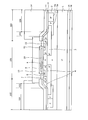
- FIG. 1 is a cross-sectional view illustrating the structure of the semiconductor device according to the first embodiment.
- the semiconductor device according to the first embodiment shown in FIG. 1 has an n-type that becomes an n-type drift layer (first semiconductor layer) 2 on the front surface of an n + -type silicon carbide substrate 1 that becomes an n + -type drain layer.
- Manufactured using a silicon carbide semiconductor substrate (semiconductor chip) in which a silicon carbide epitaxial layer and a p-type silicon carbide epitaxial layer serving as a p-type base layer (second semiconductor layer) 4 are sequentially deposited.
- a silicon carbide semiconductor substrate semiconductor chip
- a termination structure portion 102 is provided in an outer peripheral portion surrounding the periphery of the active region 101.
- the active region 101 is a region through which a main current flows in the on state.
- the termination structure 102 is a region that relaxes the electric field on the front surface side of the base of the n-type drift layer 2 and maintains a withstand voltage.
- the p-type silicon carbide epitaxial layer serving as p-type base layer 4 extends from active region 101 to the vicinity of the boundary between active region 101 and termination structure portion 102. That is, on the front surface of the silicon carbide semiconductor substrate, the outer peripheral portion of the p-type base layer 4 is removed in the vicinity of the boundary between the termination structure portion 102 and the active region 101, so that the p-type base layer 4 and n A stepped portion 103 generated between the mold drift layer 2 and the mold drift layer 2 is provided.
- the portion of the front surface of the silicon carbide semiconductor substrate on the outer side (chip end portion side) than the stepped portion 103 is a flat portion 104 that exposes the surface of the n-type drift layer 2.
- the substrate front surface (surface of a p ⁇ type region (second semiconductor region) 5a and p ⁇ type region 5b described later) in the flat portion 104 is the substrate front surface (p type base layer 4 in the active region 101).
- the surface is deeper (closer to the back surface of the substrate) than the front surface of the substrate.
- a MOS gate insulated gate made of metal-oxide film-semiconductor structure having a planar gate structure is provided on the front surface side (p-type base layer 4 side) of the silicon carbide semiconductor substrate.
- FIG. 1 shows one unit cell among one or more unit cells (functional units of elements) arranged in the active region 101.
- a p + type base region first semiconductor region
- n type drift layer 2 n type silicon carbide epitaxial layer
- the p + type base region 3 on the outermost side (on the termination structure portion 102 side) extends to the flat portion 104 of the termination structure portion 102, and the base surface of the flat portion 104 (that is, p of the termination structure portion 102). The portion where the mold base layer 4 is not deposited is exposed.
- the p + type base region 3 forms a base region together with the p type base layer 4.
- n type drift layer 2 On the surface of n type drift layer 2 opposite to the n + type silicon carbide substrate 1 side, a portion of n type drift layer 2 sandwiched between adjacent p + type base regions 3 and p A p-type base layer 4 (p-type silicon carbide epitaxial layer) is selectively deposited so as to cover a portion of the + -type base region 3 other than the portion extending to the flat portion 104.
- the impurity concentration of the p-type base layer 4 is lower than the impurity concentration of the p + -type base region 3.
- an n + -type source region (third semiconductor region) 6 and a p + -type contact region (fifth semiconductor region) 7 are selectively formed on the p + -type base region 3. Is provided.
- the n + type source region 6 and the p + type contact region 7 are in contact with each other.
- the n + type source region 6 is arranged at a position closer to an n type well region (fourth semiconductor region) 8 to be described later than the p + type contact region 7.
- n-type well region 8 that penetrates the p-type base layer 4 in the depth direction and reaches the n-type drift layer 2 is provided inside the p-type base layer 4.
- the n-type well region 8 is a JFET (Junction Field Effect Transistor) region that is sandwiched between adjacent base regions and disposed immediately below the gate electrode 10 (on the substrate side).
- N-type well region 8 forms a drift region together with n-type drift layer 2.
- a gate electrode 10 is provided on the surface of the portion of the p-type base layer 4 sandwiched between the n + -type source region 6 and the n-type well region 8 via a gate insulating film 9.
- the gate electrode 10 may be provided on the surface of the n-type well region 8 via the gate insulating film 9.
- Gate insulating film 9 may be provided on the entire front surface side of the silicon carbide semiconductor substrate except for a portion requiring a contact electrode.
- Interlayer insulating film 11 is provided on the entire front surface side of the silicon carbide semiconductor substrate so as to cover gate electrode 10.
- the source electrode (first electrode) 12 is in contact with the n + type source region 6 and the p + type contact region 7 through a contact hole penetrating the interlayer insulating film 11 in the depth direction. 10 is electrically insulated.
- the front electrode pad 13 is provided over the entire active region 101 so as to be in contact with the source electrodes 12 of all the unit cells. The end portion of the front electrode pad 13 extends on the interlayer insulating film 11 of the termination structure portion 102 and terminates, for example, inside the step portion 103 (on the active region 101 side).
- the interlayer insulating film 11 is made of, for example, polyimide so as to cover the end of the front electrode pad 13 and the outer end of the source electrode 12 of the outermost unit cell.
- a protective film 14 such as a passivation film is provided.
- the protective film 14 has a function of preventing discharge.
- n-type drift layer 2 has a surface layer on the opposite side to n + -type silicon carbide substrate 1, and has a plurality of p-type regions (p ⁇ -type region 5 a and p ⁇ -type region 5 a) having different impurity concentrations.
- p - is provided pressure-resistant structure composed of type region 5b).
- This breakdown voltage structure has a function of relaxing electric field concentration near the boundary between the active region 101 and the termination structure portion 102.
- the p ⁇ type region 5 a is provided so as to be exposed on the front surface of the base in the flat portion 104, is in contact with the outermost p + type base region 3, and the p + type base region 3 Surround the surroundings.
- the p ⁇ type region 5a extends from the flat portion 104 inward to, for example, the stepped portion 103, and is below the drain side (drain side) of the outermost p + type base region 3 extending to the flat portion 104. ) Cover the whole.
- p - type region 5b is, p - provided outside the mold area 5a, p - the contact type region 5a, and p - surrounding the type region 5a.
- p ⁇ type region 5 a and p ⁇ type region 5 b are provided in a concentric circle surrounding the periphery of active region 101, and constitute a double zone JTE (Junction Termination Extension) structure.
- the interface between p ⁇ type region 5 a and p ⁇ type region 5 b and n type drift layer 2 is located closer to the drain than the interface between p + type base region 3 and n type drift layer 2. That is, the thicknesses of the p ⁇ -type region 5a and the p ⁇ -type region 5b are larger than the thickness of the p + -type base region 3 in the flat portion 104 (depth from the front surface of the substrate).
- the substrate front surface in the termination structure portion 102 (including the step portion 103 and the flat portion 104) is covered with an interlayer insulating film 11 (or an insulating layer in which the gate insulating film 9 and the interlayer insulating film 11 are sequentially stacked).
- the p ⁇ type region 5 a and the p ⁇ type region 5 b are electrically insulated from the unit cell of the active region 101 by the interlayer insulating film 11.
- the withstand voltage structure disposed in the termination structure 102 may be another withstand voltage structure for relaxing electric field concentration, such as a multi-zone JTE structure or an FLR (Field Limiting Ring) structure, instead of the double zone JTE structure.
- the multi-zone JTE structure is adjacent so that three or more p-type regions having different impurity concentrations are concentrically surrounding the periphery of the active region 101 and p-type regions having a lower impurity concentration are arranged toward the outside. This is a pressure-resistant structure arranged.
- the FLR structure is a pressure-resistant structure in which a plurality of p-type regions are arranged concentrically around the active region 101 at a predetermined interval, and can be applied regardless of the difficulty of manufacturing.
- a back electrode (second electrode) 15 that is a drain electrode is provided from the active region 101 to the termination structure portion 102.
- the back electrode pad 16 is provided on the surface of the back electrode 15.
- FIG. 2 for example, an n + type silicon carbide substrate (semiconductor wafer) 1 doped with an n type impurity such as nitrogen (N) at an impurity concentration of about 2 ⁇ 10 19 / cm 3 is prepared. .
- n + -type silicon carbide substrate 1 may be, for example, a (000-1) surface having an off angle of about 4 degrees in the ⁇ 11-20> direction.
- an n-type impurity such as nitrogen is doped on the front surface of the n + -type silicon carbide substrate 1 as an n-type drift layer 2 with an impurity concentration of 1.0 ⁇ 10 16 / cm 3 , for example.
- An n-type silicon carbide epitaxial layer having a thickness of 10 ⁇ m is grown.
- p + type base region 3 is selectively formed on the surface layer of n type drift layer 2 in active region 101 by photolithography and ion implantation.
- the outermost p + type base region 3 is formed so as to extend to the termination structure portion 102.
- the dopant may be aluminum (Al), and the dose may be set so that the impurity concentration of the p + -type base region 3 is 1.0 ⁇ 10 18 / cm 3 .
- the thickness of the p + type base region 3 may be 0.5 ⁇ m, for example.
- the distance between adjacent p + -type base regions 3 may be 1.6 ⁇ m, for example.
- a p-type silicon carbide epitaxial layer to be the p-type base layer 4 is grown on the surface of the n-type drift layer 2 with a thickness of 0.5 ⁇ m, for example.
- the p-type base layer 4 is doped with, for example, aluminum.
- a p-type silicon carbide epitaxial layer doped with aluminum may be grown so that the impurity concentration of the p-type base layer 4 is 5.0 ⁇ 10 15 / cm 3 .
- the conductivity type of the portion of the p-type base layer 4 on the n-type drift layer 2 is inverted by photolithography and ion implantation to selectively form the n-type well region 8.
- the dopant may be nitrogen, and the dose may be set so that the impurity concentration of the n-type well region 8 is 5.0 ⁇ 10 16 / cm 3 .
- the width and thickness of the n-type well region 8 may be, for example, 2.0 ⁇ m and 0.6 ⁇ m, respectively.
- the outer peripheral portion of the p-type base layer 4 in the termination structure portion 102 is removed by photolithography and etching to expose the n-type drift layer 2 in the termination structure portion 102.
- a stepped portion 103 is formed between the p-type base layer 4 and the n-type drift layer 2 in the vicinity of the boundary between the termination structure portion 102 and the active region 101.
- a flat portion 104 formed by exposing the surface of the n-type drift layer 2 is formed outside the step portion 103 (portion outside the chip).
- the p ⁇ -type region 5a and the p ⁇ -type region 5b constituting the double zone JTE structure are formed on the surface layer of the n-type drift layer 2 exposed to the termination structure portion 102, respectively.
- the p ⁇ type region 5 a is formed so as to cover the entire lower side of the portion extending to the flat portion 104 of the outermost p + type base region 3.
- the ion implantation for forming the p ⁇ -type region 5a for example, even if the dopant is aluminum and the dose is set so that the impurity concentration of the p ⁇ -type region 5a is 6.0 ⁇ 10 17 / cm 3.
- the width and thickness of the p ⁇ type region 5a may be, for example, 80 ⁇ m and 0.5 ⁇ m, respectively.
- the width and thickness of the p ⁇ -type region 5b may be, for example, 60 ⁇ m and 0.5 ⁇ m, respectively.
- the n + type source region 6 is selectively formed on the surface layer of the p type base layer 4 on the p + type base region 3 by photolithography and ion implantation.
- the p + type contact region 7 is selectively formed on the surface layer of the p type base layer 4 on the p + type base region 3 by photolithography and ion implantation.
- heat treatment annealing
- the heat treatment temperature and heat treatment time at this time may be, for example, 1620 ° C. and 2 minutes, respectively.
- the order of forming the p ⁇ -type region 5a, the p ⁇ -type region 5b, the n + -type source region 6, the p + -type contact region 7 and the n-type well region 8 can be variously changed.
- the p ⁇ type region 5a and the p ⁇ type region 5b may be formed after the flat portion 104 is formed and before the activation heat treatment.
- the ion implantation implantation region for forming the p ⁇ -type region 5a and the ion implantation implantation region for forming the p + -type base region 3 may partially overlap. Further, the activation heat treatment may be performed for each ion implantation for forming each region.
- the front surface side of the silicon carbide semiconductor substrate is thermally oxidized to form a gate insulating film 9 having a thickness of about 100 nm, for example.
- This thermal oxidation may be performed, for example, by heat treatment at a temperature of about 1000 ° C. in a mixed atmosphere of oxygen (O 2 ) gas and hydrogen (H 2 ) gas.
- O 2 oxygen
- H 2 hydrogen
- each region formed on the surface of the p-type base layer 4 and the n-type drift layer 2 is covered with the gate insulating film 9.
- a polycrystalline silicon layer doped with, for example, phosphorus (P) is formed on the gate insulating film 9 as the gate electrode 10.
- the polycrystalline silicon layer is patterned to leave the polycrystalline silicon layer on the portion of the p-type base layer 4 sandwiched between the n + -type source region 6 and the n-type well region 8. At this time, a polycrystalline silicon layer may be left on the n-type well region 8.
- phosphorous glass (PSG) is deposited (formed) to a thickness of about 1.0 ⁇ m as the interlayer insulating film 11 so as to cover the gate insulating film 9.
- interlayer insulating film 11 and gate insulating film 9 are selectively removed by photolithography and etching to form contact holes, and n + type source region 6 and p + type contact region 7 are formed.
- heat treatment (reflow) for planarizing the interlayer insulating film 11 is performed.
- a nickel (Ni) film serving as the source electrode 12 is formed on the interlayer insulating film 11 so as to be embedded in the contact hole.
- the nickel film is selectively removed by photolithography and etching, leaving the nickel film only on the n + -type source region 6 and the p + -type contact region 7 exposed in the contact holes.
- a nickel film serving as the lowest layer among the plurality of metal films constituting the back electrode 15 is formed on the entire back surface of the silicon carbide semiconductor substrate (the back surface of the n + -type silicon carbide substrate 1).
- a front electrode pad 13 is deposited (formed) on the entire front surface of the silicon carbide semiconductor substrate so as to cover the source electrode 12 by, for example, sputtering.
- the thickness of the front electrode pad 13 on the interlayer insulating film 11 may be about 5 ⁇ m, for example.
- the front electrode pad 13 may be formed of, for example, a metal whose main component is aluminum.
- the front surface electrode pad 13 is patterned to expose the interlayer insulating film 11 in the termination structure portion 102.
- a polyimide film is formed as the protective film 14 on the surface of the interlayer insulating film 11 and the front electrode pad 13.
- the protective film 14 is selectively removed by photolithography and etching to expose the front electrode pad 13, and the front electrode pad 13 is formed on the interlayer insulating film 11 in the termination structure 102.
- the protective film 14 is left so as to extend to the end.
- a laminated film formed by sequentially laminating, for example, a titanium (Ti) film, a nickel film, and a gold (Au) film as the back electrode pad 16 is formed on the entire surface of the nickel silicide film on the back surface of the silicon carbide semiconductor substrate. Thereafter, the semiconductor wafer is cut (diced) into chips to complete the MOSFET shown in FIG.
- the outermost p + type base region extends to the flat portion of the termination structure portion, and the innermost p type region constituting the breakdown voltage structure is included.
- the outer part of the outermost p + type base region covers the entire lower side of the portion extending to the flat part, so that when the high voltage is applied to the drain electrode, the outermost p + type base region
- the electric field can be concentrated on the outer peripheral end portion or on a plurality of p-type regions constituting the breakdown voltage structure. Therefore, even when the p-type base layer having a low impurity concentration is formed by epitaxial growth in the active region to reduce the on-resistance, the electric field is concentrated on the stepped portion formed by forming the p-type base layer. Can be prevented.
- the depletion layer can be prevented from extending to the p-type base layer side having a low impurity concentration formed by epitaxial growth. As a result, it is possible to prevent the breakdown voltage from being lowered, so that the breakdown voltage can be improved as compared with the conventional case. Therefore, a semiconductor device with low on-resistance and high breakdown voltage can be provided. Further, according to the first embodiment, an opening of a mask used for ion implantation for forming the outermost p + -type base region and ion implantation for forming the innermost p-type region constituting the breakdown voltage structure. By appropriately changing the range, a low on-resistance and high breakdown voltage semiconductor device can be manufactured without adding a new process.
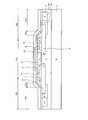
- FIG. 8 is a cross-sectional view illustrating the structure of the semiconductor device according to the second embodiment.
- the difference between the semiconductor device according to the second embodiment and the semiconductor device according to the first embodiment is that of the two p-type regions (p ⁇ -type region 25a and p ⁇ -type region 5b) constituting the double zone JTE structure.
- the p ⁇ type region 25a on the inner side of the substrate is extended from the flat portion 104 to the active region 101 along the front surface of the base so as to overlap the outer peripheral portion of the p type base layer 4.
- the p ⁇ type region 25 a includes a portion extending to the flat portion 104 and the step portion 103 of the p + type base region 3, and a portion extending to the step portion 103 of the p type base layer 4. For example, is in contact with the outermost p + -type contact region 7 (hatched portion).
- the manufacturing method of the semiconductor device according to the second embodiment is the same as the manufacturing method of the semiconductor device according to the first embodiment, except that ion implantation for forming the p ⁇ -type region 25a is performed to the outer peripheral portion of the p-type base layer 4. What is necessary is just to go to the wide range which overlaps. At this time, the ion implantation implantation region for forming the p ⁇ -type region 25a and the ion implantation implantation region for forming the p + -type base region 3 may partially overlap.
- the innermost p-type region constituting the breakdown voltage structure is provided so as to overlap the portion of the outermost p + -type base region that extends to the flat portion.
- the innermost p-type region constituting the breakdown voltage structure is provided so as to overlap part of the p-type base layer, thereby increasing the impurity concentration in the outer peripheral portion of the p-type base layer. can do. This can prevent the depletion layer from extending into the p-type base layer.
- the impurity concentration in the outer peripheral portion of the p-type base layer can be increased, and variations in breakdown voltage due to process variations can be avoided.
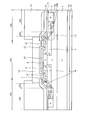
- FIG. 9 is a cross-sectional view illustrating the structure of the semiconductor device according to the third embodiment.
- the semiconductor device according to the third embodiment is different from the semiconductor device according to the first embodiment in that the outermost p + -type contact region (fifth semiconductor region) 27 is arranged along the front surface of the substrate and the active region 101. Is extended to the flat portion 104 and is provided so as to overlap the inner peripheral portion of the p ⁇ type region 5a on the inner side of the two p type regions constituting the double zone JTE structure.
- the outermost p + -type contact region 27 extends to the portion of the p-type base layer 4 that extends to the stepped portion 103 and the flat portion 104 and the stepped portion 103 of the p + -type base region 3. And a portion covering the lower side of the p + type base region 3 of the p ⁇ type region 5a (hatched portion).
- the manufacturing method of the semiconductor device according to the third embodiment is the same as the manufacturing method of the semiconductor device according to the first embodiment, except that ion implantation for forming the p + -type contact region 27 is performed on the inner peripheral portion of the p ⁇ -type region 5a. It is sufficient to go over a wide range overlapping. At this time, the ion implantation for forming the p + -type contact region 27 and the implantation region for ion implantation for forming the p + -type base region 3 may partially overlap.
- the entire lower side of the portion extending to flat portion 104 of p + type base region 3 is covered with outermost p + type contact region 27. Therefore, the lower side of the portion extending to the flat portion 104 of the p + type base region 3 may not be covered with the p ⁇ type region 5a. That is, the outermost p + -type contact region 27 includes a portion of the p-type base layer 4 that extends to the stepped portion 103 and a portion of the p + -type base region 3 that extends to the flat portion 104 and the stepped portion 103. And may be provided so as to overlap each other (not shown).
- the outermost p + type contact region 27 corresponds to the p ⁇ type region 5a. It may be in a state extending to the extent that it is in contact with the inner peripheral edge.
- the drain electrode When a high voltage is applied, the electric field can be concentrated on the outer peripheral edge of the outermost p + -type contact region or on a plurality of p-type regions constituting the breakdown voltage structure. Thereby, the effect similar to Embodiment 1 can be acquired.
- the outermost portion of the p-type base layer is provided by providing the outermost p + -type contact region so as to overlap with a part of the innermost p-type region constituting the breakdown voltage structure. The impurity concentration of can be increased. Thereby, the same effect as Embodiment 2 can be acquired.
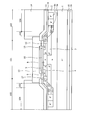
- FIG. 10 is a cross-sectional view showing the structure of the semiconductor device of Comparative Example 1.
- FIG. 11 is a characteristic diagram showing the relationship between the impurity concentration of the inner p ⁇ -type region constituting the double zone JTE structure and the breakdown voltage.
- the inner p ⁇ type region 25a constituting the double zone JTE structure is overlapped with a part of the p type base layer 4 under the above-described various conditions.
- a MOSFET (see FIG. 8) provided in (1) was fabricated (hereinafter referred to as an example).
- Example and Comparative Example 1 the etching amount (etching depth) of the epitaxial layer when the stepped portion 103 is formed in the termination structure portion 102 is set to a standard 0.7 ⁇ m (hereinafter referred to as a standard etching amount), respectively. Two samples having a depth of 0.9 ⁇ m (hereinafter referred to as excessive etching amount) deeper than the standard were prepared.
- the impurity concentration of the outer p ⁇ -type region 5b constituting the double zone JTE structure was set to half the impurity concentration of the inner p ⁇ -type regions 25a and 35a.
- the configuration other than the p ⁇ type region 35a of Comparative Example 1 is the same as that of the example.
- FIG. 1 The configuration other than the p ⁇ type region 35a of Comparative Example 1 is the same as that of the example.
- FIG. 11 shows the result of simulating the relationship between the impurity concentration and the breakdown voltage of the p ⁇ -type regions 25a and 35a of these examples and comparative example 1.
- the horizontal axis in FIG. 11 is the impurity concentration of the p ⁇ -type regions 25a and 35a, and the vertical axis is the breakdown voltage BVdss.
- the breakdown voltage was lowered when the impurity concentration in the p ⁇ -type region 25a was less than 1.00 ⁇ 10 17 / cm 3 in both the standard etching amount and the excessive etching amount. It was. From this, it was confirmed that the example has a structure with little adverse effect due to process variation.
- FIG. 12 is a cross-sectional view showing the structure of the semiconductor device of Comparative Example 2.
- FIG. 13 is a characteristic diagram showing the electric field strength distribution near the boundary between the active region and the termination structure.
- FIG. 13A shows the electric field strength distribution of the termination structure 111 (see FIG. 8) of the example.
- FIG. 13B shows the electric field intensity distribution of the termination structure 121 (see FIG. 10) of Comparative Example 1.
- FIG. 13C shows the electric field strength distribution of the termination structure portion 122 (see FIG. 12) of Comparative Example 2.
- the outermost p + type base region 33 is not extended to the flat portion 104.
- the configuration of Comparative Example 2 other than the p + type base region 33 is the same as that of Comparative Example 1.
- the outermost p + type base region 3 extends to the flat portion 104 and extends to the flat portion 104 of the p + type base region 3 as in the embodiment. It was confirmed that the high breakdown voltage can be maintained by covering the entire lower side of the portion to be covered with the p ⁇ -type region 25a.
- the outermost p + type base region 3 is used in the semiconductor device according to the first and third embodiments.
- the present invention is not limited to the above-described embodiments, and various modifications can be made without departing from the spirit of the present invention.
- the dimensions and impurity concentration of each part are appropriately set according to required specifications.
- the main surface (front surface) of the silicon carbide substrate is taken as an example in which the (000-1) surface having an off angle of about 4 degrees in the ⁇ 11-20> direction is used.
- the present invention is not limited to this, and the plane orientation of the main surface of the silicon carbide substrate can be variously changed according to the design conditions and the like. Further, the present invention has the same effect when applied to a MOSFET having a trench gate structure.
- the MOSFET is described as an example.
- the present invention can be applied to a MOS type semiconductor device such as an IGBT having a MOS gate structure on the base surface side.
- a silicon carbide semiconductor is used as an example.
- the present invention is not limited to this, and other wide band gap semiconductors such as gallium nitride (GaN) and diamond, and silicon (Si) semiconductors. The same effect can be obtained when using.
- the first conductivity type is n-type and the second conductivity type is p-type.
- the first conductivity type is p-type and the second conductivity type is n-type. It holds.
- the semiconductor device according to the present invention is useful for a high breakdown voltage semiconductor device used for a power supply device such as a power conversion device and various industrial machines, and particularly, a semiconductor device using a wide band gap semiconductor. Suitable for
- n + type silicon carbide substrate 2 n type drift layer 3 p + type base region 4 p type base layer 5a, 25a p ⁇ type region 5b p ⁇ type region 6 n + type source region 7, 27 p + type contact region 8 n-type well region 9 gate insulating film 10 gate electrode 11 interlayer insulating film 12 source electrode 13 front surface electrode pad 14 protective film 15 back surface electrode 16 back surface electrode pad 101 active region 102 termination structure portion 103 stepped portion 104 flat portion
Landscapes
- Electrodes Of Semiconductors (AREA)
Abstract
Selon l'invention, une structure de grille MOS est située sur le côté couche de base du type p (4) d'un corps semi-conducteur au carbure de silicium obtenu par croissance épitaxiale successive d'une couche de migration du type n (2) et de la couche de base du type p (4) sur une surface avant d'un substrat de carbure de silicium du type n+ (1). Sur une surface avant du corps, une partie échelon (103) produite entre la couche de base du type p (4) et la couche de migration du type n (2), et une partie plate (104) disposée davantage vers le côté extérieur que la partie échelon sont ménagées dans une partie de structure de terminaison (102). Dans une couche de surface de la couche de migration du type n (2), une zone de base du type p+ (3) constituant la structure de grille MOS est formée en contact avec la couche de base du type p (4). La zone de base du type p+ la plus à l'extérieur (3) s'étend depuis une zone active (101) jusqu'à la partie plate (104), et la totalité d'un côté inférieur de cette partie est recouverte par une zone du type p- la plus à l'intérieur (5a) qui constitue une structure résistant à la tension ménagée dans la partie plate (104). De cette manière, un dispositif à semi-conducteurs présentant une plus grande résistance à la tension peut être obtenu.
Priority Applications (2)
| Application Number | Priority Date | Filing Date | Title |
|---|---|---|---|
| JP2016557354A JP6052481B2 (ja) | 2014-12-25 | 2015-12-16 | 半導体装置 |
| US15/581,021 US9793392B2 (en) | 2014-12-25 | 2017-04-28 | Semiconductor device |
Applications Claiming Priority (2)
| Application Number | Priority Date | Filing Date | Title |
|---|---|---|---|
| JP2014263020 | 2014-12-25 | ||
| JP2014-263020 | 2014-12-25 |
Related Child Applications (1)
| Application Number | Title | Priority Date | Filing Date |
|---|---|---|---|
| US15/581,021 Continuation US9793392B2 (en) | 2014-12-25 | 2017-04-28 | Semiconductor device |
Publications (1)
| Publication Number | Publication Date |
|---|---|
| WO2016104264A1 true WO2016104264A1 (fr) | 2016-06-30 |
Family
ID=56150289
Family Applications (1)
| Application Number | Title | Priority Date | Filing Date |
|---|---|---|---|
| PCT/JP2015/085148 Ceased WO2016104264A1 (fr) | 2014-12-25 | 2015-12-16 | Dispositif à semi-conducteurs |
Country Status (3)
| Country | Link |
|---|---|
| US (1) | US9793392B2 (fr) |
| JP (1) | JP6052481B2 (fr) |
| WO (1) | WO2016104264A1 (fr) |
Cited By (9)
| Publication number | Priority date | Publication date | Assignee | Title |
|---|---|---|---|---|
| JP2018082056A (ja) * | 2016-11-16 | 2018-05-24 | 富士電機株式会社 | 半導体装置および半導体装置の製造方法 |
| JP2018110164A (ja) * | 2016-12-28 | 2018-07-12 | 富士電機株式会社 | 半導体装置 |
| JP2018137410A (ja) * | 2017-02-23 | 2018-08-30 | 富士電機株式会社 | 半導体装置の製造方法 |
| WO2019093465A1 (fr) * | 2017-11-13 | 2019-05-16 | 三菱電機株式会社 | Dispositif à semi-conducteurs au carbure de silicium et procédé de fabrication de dispositif à semi-conducteurs au carbure de silicium |
| JP2019149477A (ja) * | 2018-02-27 | 2019-09-05 | 三菱電機株式会社 | 半導体装置およびその製造方法並びに電力変換装置 |
| JP2020136320A (ja) * | 2019-02-13 | 2020-08-31 | 株式会社豊田中央研究所 | 窒化物半導体装置 |
| JP2021010027A (ja) * | 2020-10-16 | 2021-01-28 | 富士電機株式会社 | 半導体装置および半導体装置の製造方法 |
| JPWO2021079471A1 (fr) * | 2019-10-24 | 2021-04-29 | ||
| JP2023549543A (ja) * | 2020-11-17 | 2023-11-27 | ロベルト・ボッシュ・ゲゼルシャフト・ミト・ベシュレンクテル・ハフツング | 縦型半導体素子およびその製造方法 |
Families Citing this family (7)
| Publication number | Priority date | Publication date | Assignee | Title |
|---|---|---|---|---|
| WO2018016029A1 (fr) * | 2016-07-20 | 2018-01-25 | 三菱電機株式会社 | Dispositif à semi-conducteurs et son procédé de fabrication |
| CN110199396B (zh) * | 2017-01-26 | 2022-06-24 | 三菱电机株式会社 | 半导体装置的制造方法 |
| WO2019123717A1 (fr) * | 2017-12-19 | 2019-06-27 | 三菱電機株式会社 | Dispositif à semi-conducteur au carbure de silicium et dispositif de conversion de puissance |
| JP6862381B2 (ja) * | 2018-03-02 | 2021-04-21 | 株式会社東芝 | 半導体装置 |
| JP6827433B2 (ja) * | 2018-03-02 | 2021-02-10 | 株式会社東芝 | 半導体装置 |
| US11158703B2 (en) * | 2019-06-05 | 2021-10-26 | Microchip Technology Inc. | Space efficient high-voltage termination and process for fabricating same |
| US11605732B2 (en) | 2019-11-06 | 2023-03-14 | Semiconductor Components Industries, Llc | Power device with graded channel |
Citations (3)
| Publication number | Priority date | Publication date | Assignee | Title |
|---|---|---|---|---|
| JP2006147789A (ja) * | 2004-11-18 | 2006-06-08 | National Institute Of Advanced Industrial & Technology | 炭化ケイ素mos電界効果トランジスタおよびその製造方法 |
| JP2008098536A (ja) * | 2006-10-16 | 2008-04-24 | National Institute Of Advanced Industrial & Technology | 炭化ケイ素半導体装置およびその製造方法 |
| JP2013232564A (ja) * | 2012-04-27 | 2013-11-14 | National Institute Of Advanced Industrial & Technology | 半導体装置および半導体装置の製造方法 |
Family Cites Families (5)
| Publication number | Priority date | Publication date | Assignee | Title |
|---|---|---|---|---|
| JP4198302B2 (ja) * | 2000-06-07 | 2008-12-17 | 三菱電機株式会社 | 半導体装置 |
| US6781194B2 (en) * | 2001-04-11 | 2004-08-24 | Silicon Semiconductor Corporation | Vertical power devices having retrograded-doped transition regions and insulated trench-based electrodes therein |
| JP4731816B2 (ja) * | 2004-01-26 | 2011-07-27 | 三菱電機株式会社 | 半導体装置 |
| JP4545800B2 (ja) | 2006-02-07 | 2010-09-15 | 三菱電機株式会社 | 炭化珪素半導体装置およびその製造方法 |
| JP4900662B2 (ja) * | 2006-03-02 | 2012-03-21 | 独立行政法人産業技術総合研究所 | ショットキーダイオードを内蔵した炭化ケイ素mos電界効果トランジスタおよびその製造方法 |
-
2015
- 2015-12-16 JP JP2016557354A patent/JP6052481B2/ja active Active
- 2015-12-16 WO PCT/JP2015/085148 patent/WO2016104264A1/fr not_active Ceased
-
2017
- 2017-04-28 US US15/581,021 patent/US9793392B2/en active Active
Patent Citations (3)
| Publication number | Priority date | Publication date | Assignee | Title |
|---|---|---|---|---|
| JP2006147789A (ja) * | 2004-11-18 | 2006-06-08 | National Institute Of Advanced Industrial & Technology | 炭化ケイ素mos電界効果トランジスタおよびその製造方法 |
| JP2008098536A (ja) * | 2006-10-16 | 2008-04-24 | National Institute Of Advanced Industrial & Technology | 炭化ケイ素半導体装置およびその製造方法 |
| JP2013232564A (ja) * | 2012-04-27 | 2013-11-14 | National Institute Of Advanced Industrial & Technology | 半導体装置および半導体装置の製造方法 |
Cited By (15)
| Publication number | Priority date | Publication date | Assignee | Title |
|---|---|---|---|---|
| JP2018082056A (ja) * | 2016-11-16 | 2018-05-24 | 富士電機株式会社 | 半導体装置および半導体装置の製造方法 |
| JP2018110164A (ja) * | 2016-12-28 | 2018-07-12 | 富士電機株式会社 | 半導体装置 |
| JP2018137410A (ja) * | 2017-02-23 | 2018-08-30 | 富士電機株式会社 | 半導体装置の製造方法 |
| WO2019093465A1 (fr) * | 2017-11-13 | 2019-05-16 | 三菱電機株式会社 | Dispositif à semi-conducteurs au carbure de silicium et procédé de fabrication de dispositif à semi-conducteurs au carbure de silicium |
| JPWO2019093465A1 (ja) * | 2017-11-13 | 2020-04-23 | 三菱電機株式会社 | 炭化珪素半導体装置、および、炭化珪素半導体装置の製造方法 |
| JP2019149477A (ja) * | 2018-02-27 | 2019-09-05 | 三菱電機株式会社 | 半導体装置およびその製造方法並びに電力変換装置 |
| JP2020136320A (ja) * | 2019-02-13 | 2020-08-31 | 株式会社豊田中央研究所 | 窒化物半導体装置 |
| JP7216564B2 (ja) | 2019-02-13 | 2023-02-01 | 株式会社豊田中央研究所 | 窒化物半導体装置 |
| JPWO2021079471A1 (fr) * | 2019-10-24 | 2021-04-29 | ||
| WO2021079471A1 (fr) * | 2019-10-24 | 2021-04-29 | 株式会社デンソー | Dispositif à semi-conducteur et son procédé de fabrication |
| JP7226580B2 (ja) | 2019-10-24 | 2023-02-21 | 株式会社デンソー | 半導体装置とその製造方法 |
| JP2021010027A (ja) * | 2020-10-16 | 2021-01-28 | 富士電機株式会社 | 半導体装置および半導体装置の製造方法 |
| JP7074173B2 (ja) | 2020-10-16 | 2022-05-24 | 富士電機株式会社 | 半導体装置および半導体装置の製造方法 |
| JP2023549543A (ja) * | 2020-11-17 | 2023-11-27 | ロベルト・ボッシュ・ゲゼルシャフト・ミト・ベシュレンクテル・ハフツング | 縦型半導体素子およびその製造方法 |
| JP7555490B2 (ja) | 2020-11-17 | 2024-09-24 | ロベルト・ボッシュ・ゲゼルシャフト・ミト・ベシュレンクテル・ハフツング | 縦型半導体素子およびその製造方法 |
Also Published As
| Publication number | Publication date |
|---|---|
| JP6052481B2 (ja) | 2016-12-27 |
| US9793392B2 (en) | 2017-10-17 |
| US20170229573A1 (en) | 2017-08-10 |
| JPWO2016104264A1 (ja) | 2017-04-27 |
Similar Documents
| Publication | Publication Date | Title |
|---|---|---|
| JP6052481B2 (ja) | 半導体装置 | |
| JP6766889B2 (ja) | 半導体装置および半導体装置の製造方法 | |
| JP7087280B2 (ja) | 炭化珪素半導体装置および炭化珪素半導体装置の製造方法 | |
| JP6911486B2 (ja) | 炭化珪素半導体装置および炭化珪素半導体装置の製造方法 | |
| JP6194779B2 (ja) | 半導体装置および半導体装置の製造方法 | |
| JP6705155B2 (ja) | 半導体装置および半導体装置の製造方法 | |
| WO2013161449A1 (fr) | Dispositif semi-conducteur et procédé de fabrication d'un dispositif semi-conducteur | |
| JP6561759B2 (ja) | 半導体装置および半導体装置の製造方法 | |
| WO2016013472A1 (fr) | Dispositif à semi-conducteurs et procédé de fabrication de dispositif à semi-conducteurs | |
| JP6862782B2 (ja) | 半導体装置および半導体装置の製造方法 | |
| JP2019029501A (ja) | 半導体装置および半導体装置の製造方法 | |
| JP2017152732A (ja) | 半導体装置および半導体装置の製造方法 | |
| JP6589263B2 (ja) | 半導体装置 | |
| JP2017092364A (ja) | 半導体装置および半導体装置の製造方法 | |
| JP6399161B2 (ja) | 半導体装置および半導体装置の製造方法 | |
| JP6737379B2 (ja) | 半導体装置 | |
| JP7074173B2 (ja) | 半導体装置および半導体装置の製造方法 | |
| JP2016058661A (ja) | 半導体装置 | |
| WO2019077878A1 (fr) | Dispositif à semi-conducteur au carbure de silicium et procédé de fabrication associé | |
| JP6350760B2 (ja) | 半導体装置および半導体装置の製造方法 | |
| JP6891448B2 (ja) | 半導体装置および半導体装置の製造方法 | |
| JP6523621B2 (ja) | 半導体装置および半導体装置の製造方法 | |
| JP6265278B2 (ja) | 炭化珪素半導体装置およびその製造方法 |
Legal Events
| Date | Code | Title | Description |
|---|---|---|---|
| 121 | Ep: the epo has been informed by wipo that ep was designated in this application |
Ref document number: 15872833 Country of ref document: EP Kind code of ref document: A1 |
|
| ENP | Entry into the national phase |
Ref document number: 2016557354 Country of ref document: JP Kind code of ref document: A |
|
| NENP | Non-entry into the national phase |
Ref country code: DE |
|
| 122 | Ep: pct application non-entry in european phase |
Ref document number: 15872833 Country of ref document: EP Kind code of ref document: A1 |