WO2019093465A1 - Dispositif à semi-conducteurs au carbure de silicium et procédé de fabrication de dispositif à semi-conducteurs au carbure de silicium - Google Patents
Dispositif à semi-conducteurs au carbure de silicium et procédé de fabrication de dispositif à semi-conducteurs au carbure de silicium Download PDFInfo
- Publication number
- WO2019093465A1 WO2019093465A1 PCT/JP2018/041633 JP2018041633W WO2019093465A1 WO 2019093465 A1 WO2019093465 A1 WO 2019093465A1 JP 2018041633 W JP2018041633 W JP 2018041633W WO 2019093465 A1 WO2019093465 A1 WO 2019093465A1
- Authority
- WO
- WIPO (PCT)
- Prior art keywords
- diffusion layer
- silicon carbide
- carbide semiconductor
- layer
- semiconductor device
- Prior art date
- Legal status (The legal status is an assumption and is not a legal conclusion. Google has not performed a legal analysis and makes no representation as to the accuracy of the status listed.)
- Ceased
Links
Images


Classifications
-
- H—ELECTRICITY
- H10—SEMICONDUCTOR DEVICES; ELECTRIC SOLID-STATE DEVICES NOT OTHERWISE PROVIDED FOR
- H10D—INORGANIC ELECTRIC SEMICONDUCTOR DEVICES
- H10D30/00—Field-effect transistors [FET]
- H10D30/60—Insulated-gate field-effect transistors [IGFET]
- H10D30/64—Double-diffused metal-oxide semiconductor [DMOS] FETs
- H10D30/66—Vertical DMOS [VDMOS] FETs
-
- H—ELECTRICITY
- H10—SEMICONDUCTOR DEVICES; ELECTRIC SOLID-STATE DEVICES NOT OTHERWISE PROVIDED FOR
- H10D—INORGANIC ELECTRIC SEMICONDUCTOR DEVICES
- H10D12/00—Bipolar devices controlled by the field effect, e.g. insulated-gate bipolar transistors [IGBT]
- H10D12/01—Manufacture or treatment
- H10D12/031—Manufacture or treatment of IGBTs
-
- H—ELECTRICITY
- H10—SEMICONDUCTOR DEVICES; ELECTRIC SOLID-STATE DEVICES NOT OTHERWISE PROVIDED FOR
- H10D—INORGANIC ELECTRIC SEMICONDUCTOR DEVICES
- H10D30/00—Field-effect transistors [FET]
- H10D30/01—Manufacture or treatment
- H10D30/021—Manufacture or treatment of FETs having insulated gates [IGFET]
- H10D30/028—Manufacture or treatment of FETs having insulated gates [IGFET] of double-diffused metal oxide semiconductor [DMOS] FETs
- H10D30/0291—Manufacture or treatment of FETs having insulated gates [IGFET] of double-diffused metal oxide semiconductor [DMOS] FETs of vertical DMOS [VDMOS] FETs
-
- H—ELECTRICITY
- H10—SEMICONDUCTOR DEVICES; ELECTRIC SOLID-STATE DEVICES NOT OTHERWISE PROVIDED FOR
- H10D—INORGANIC ELECTRIC SEMICONDUCTOR DEVICES
- H10D30/00—Field-effect transistors [FET]
- H10D30/60—Insulated-gate field-effect transistors [IGFET]
- H10D30/64—Double-diffused metal-oxide semiconductor [DMOS] FETs
- H10D30/65—Lateral DMOS [LDMOS] FETs
-
- H—ELECTRICITY
- H10—SEMICONDUCTOR DEVICES; ELECTRIC SOLID-STATE DEVICES NOT OTHERWISE PROVIDED FOR
- H10D—INORGANIC ELECTRIC SEMICONDUCTOR DEVICES
- H10D62/00—Semiconductor bodies, or regions thereof, of devices having potential barriers
- H10D62/10—Shapes, relative sizes or dispositions of the regions of the semiconductor bodies; Shapes of the semiconductor bodies
- H10D62/124—Shapes, relative sizes or dispositions of the regions of semiconductor bodies or of junctions between the regions
- H10D62/126—Top-view geometrical layouts of the regions or the junctions
- H10D62/127—Top-view geometrical layouts of the regions or the junctions of cellular field-effect devices, e.g. multicellular DMOS transistors or IGBTs
-
- H—ELECTRICITY
- H10—SEMICONDUCTOR DEVICES; ELECTRIC SOLID-STATE DEVICES NOT OTHERWISE PROVIDED FOR
- H10D—INORGANIC ELECTRIC SEMICONDUCTOR DEVICES
- H10D62/00—Semiconductor bodies, or regions thereof, of devices having potential barriers
- H10D62/10—Shapes, relative sizes or dispositions of the regions of the semiconductor bodies; Shapes of the semiconductor bodies
- H10D62/13—Semiconductor regions connected to electrodes carrying current to be rectified, amplified or switched, e.g. source or drain regions
- H10D62/149—Source or drain regions of field-effect devices
- H10D62/151—Source or drain regions of field-effect devices of IGFETs
- H10D62/152—Source regions of DMOS transistors
- H10D62/154—Dispositions
-
- H—ELECTRICITY
- H10—SEMICONDUCTOR DEVICES; ELECTRIC SOLID-STATE DEVICES NOT OTHERWISE PROVIDED FOR
- H10D—INORGANIC ELECTRIC SEMICONDUCTOR DEVICES
- H10D62/00—Semiconductor bodies, or regions thereof, of devices having potential barriers
- H10D62/10—Shapes, relative sizes or dispositions of the regions of the semiconductor bodies; Shapes of the semiconductor bodies
- H10D62/13—Semiconductor regions connected to electrodes carrying current to be rectified, amplified or switched, e.g. source or drain regions
- H10D62/149—Source or drain regions of field-effect devices
- H10D62/151—Source or drain regions of field-effect devices of IGFETs
- H10D62/156—Drain regions of DMOS transistors
- H10D62/158—Dispositions
-
- H—ELECTRICITY
- H10—SEMICONDUCTOR DEVICES; ELECTRIC SOLID-STATE DEVICES NOT OTHERWISE PROVIDED FOR
- H10D—INORGANIC ELECTRIC SEMICONDUCTOR DEVICES
- H10D62/00—Semiconductor bodies, or regions thereof, of devices having potential barriers
- H10D62/10—Shapes, relative sizes or dispositions of the regions of the semiconductor bodies; Shapes of the semiconductor bodies
- H10D62/17—Semiconductor regions connected to electrodes not carrying current to be rectified, amplified or switched, e.g. channel regions
- H10D62/393—Body regions of DMOS transistors or IGBTs
-
- H—ELECTRICITY
- H10—SEMICONDUCTOR DEVICES; ELECTRIC SOLID-STATE DEVICES NOT OTHERWISE PROVIDED FOR
- H10D—INORGANIC ELECTRIC SEMICONDUCTOR DEVICES
- H10D62/00—Semiconductor bodies, or regions thereof, of devices having potential barriers
- H10D62/80—Semiconductor bodies, or regions thereof, of devices having potential barriers characterised by the materials
- H10D62/83—Semiconductor bodies, or regions thereof, of devices having potential barriers characterised by the materials being Group IV materials, e.g. B-doped Si or undoped Ge
- H10D62/832—Semiconductor bodies, or regions thereof, of devices having potential barriers characterised by the materials being Group IV materials, e.g. B-doped Si or undoped Ge being Group IV materials comprising two or more elements, e.g. SiGe
- H10D62/8325—Silicon carbide
-
- H—ELECTRICITY
- H10—SEMICONDUCTOR DEVICES; ELECTRIC SOLID-STATE DEVICES NOT OTHERWISE PROVIDED FOR
- H10D—INORGANIC ELECTRIC SEMICONDUCTOR DEVICES
- H10D64/00—Electrodes of devices having potential barriers
- H10D64/20—Electrodes characterised by their shapes, relative sizes or dispositions
- H10D64/27—Electrodes not carrying the current to be rectified, amplified, oscillated or switched, e.g. gates
- H10D64/311—Gate electrodes for field-effect devices
- H10D64/411—Gate electrodes for field-effect devices for FETs
- H10D64/511—Gate electrodes for field-effect devices for FETs for IGFETs
- H10D64/514—Gate electrodes for field-effect devices for FETs for IGFETs characterised by the insulating layers
-
- H—ELECTRICITY
- H10—SEMICONDUCTOR DEVICES; ELECTRIC SOLID-STATE DEVICES NOT OTHERWISE PROVIDED FOR
- H10D—INORGANIC ELECTRIC SEMICONDUCTOR DEVICES
- H10D64/00—Electrodes of devices having potential barriers
- H10D64/20—Electrodes characterised by their shapes, relative sizes or dispositions
- H10D64/27—Electrodes not carrying the current to be rectified, amplified, oscillated or switched, e.g. gates
- H10D64/311—Gate electrodes for field-effect devices
- H10D64/411—Gate electrodes for field-effect devices for FETs
- H10D64/511—Gate electrodes for field-effect devices for FETs for IGFETs
- H10D64/517—Gate electrodes for field-effect devices for FETs for IGFETs characterised by the conducting layers
-
- H—ELECTRICITY
- H10—SEMICONDUCTOR DEVICES; ELECTRIC SOLID-STATE DEVICES NOT OTHERWISE PROVIDED FOR
- H10P—GENERIC PROCESSES OR APPARATUS FOR THE MANUFACTURE OR TREATMENT OF DEVICES COVERED BY CLASS H10
- H10P30/00—Ion implantation into wafers, substrates or parts of devices
- H10P30/20—Ion implantation into wafers, substrates or parts of devices into semiconductor materials, e.g. for doping
- H10P30/22—Ion implantation into wafers, substrates or parts of devices into semiconductor materials, e.g. for doping using masks
-
- H—ELECTRICITY
- H10—SEMICONDUCTOR DEVICES; ELECTRIC SOLID-STATE DEVICES NOT OTHERWISE PROVIDED FOR
- H10P—GENERIC PROCESSES OR APPARATUS FOR THE MANUFACTURE OR TREATMENT OF DEVICES COVERED BY CLASS H10
- H10P76/00—Manufacture or treatment of masks on semiconductor bodies, e.g. by lithography or photolithography
- H10P76/20—Manufacture or treatment of masks on semiconductor bodies, e.g. by lithography or photolithography of masks comprising organic materials
- H10P76/204—Manufacture or treatment of masks on semiconductor bodies, e.g. by lithography or photolithography of masks comprising organic materials of organic photoresist masks
-
- H—ELECTRICITY
- H10—SEMICONDUCTOR DEVICES; ELECTRIC SOLID-STATE DEVICES NOT OTHERWISE PROVIDED FOR
- H10P—GENERIC PROCESSES OR APPARATUS FOR THE MANUFACTURE OR TREATMENT OF DEVICES COVERED BY CLASS H10
- H10P76/00—Manufacture or treatment of masks on semiconductor bodies, e.g. by lithography or photolithography
- H10P76/40—Manufacture or treatment of masks on semiconductor bodies, e.g. by lithography or photolithography of masks comprising inorganic materials
- H10P76/408—Manufacture or treatment of masks on semiconductor bodies, e.g. by lithography or photolithography of masks comprising inorganic materials characterised by their sizes, orientations, dispositions, behaviours or shapes
-
- H—ELECTRICITY
- H10—SEMICONDUCTOR DEVICES; ELECTRIC SOLID-STATE DEVICES NOT OTHERWISE PROVIDED FOR
- H10D—INORGANIC ELECTRIC SEMICONDUCTOR DEVICES
- H10D12/00—Bipolar devices controlled by the field effect, e.g. insulated-gate bipolar transistors [IGBT]
- H10D12/01—Manufacture or treatment
- H10D12/031—Manufacture or treatment of IGBTs
- H10D12/032—Manufacture or treatment of IGBTs of vertical IGBTs
-
- H—ELECTRICITY
- H10—SEMICONDUCTOR DEVICES; ELECTRIC SOLID-STATE DEVICES NOT OTHERWISE PROVIDED FOR
- H10D—INORGANIC ELECTRIC SEMICONDUCTOR DEVICES
- H10D12/00—Bipolar devices controlled by the field effect, e.g. insulated-gate bipolar transistors [IGBT]
- H10D12/411—Insulated-gate bipolar transistors [IGBT]
- H10D12/441—Vertical IGBTs
-
- H—ELECTRICITY
- H10—SEMICONDUCTOR DEVICES; ELECTRIC SOLID-STATE DEVICES NOT OTHERWISE PROVIDED FOR
- H10P—GENERIC PROCESSES OR APPARATUS FOR THE MANUFACTURE OR TREATMENT OF DEVICES COVERED BY CLASS H10
- H10P30/00—Ion implantation into wafers, substrates or parts of devices
- H10P30/20—Ion implantation into wafers, substrates or parts of devices into semiconductor materials, e.g. for doping
- H10P30/202—Ion implantation into wafers, substrates or parts of devices into semiconductor materials, e.g. for doping characterised by the semiconductor materials
- H10P30/204—Ion implantation into wafers, substrates or parts of devices into semiconductor materials, e.g. for doping characterised by the semiconductor materials into Group IV semiconductors
- H10P30/2042—Ion implantation into wafers, substrates or parts of devices into semiconductor materials, e.g. for doping characterised by the semiconductor materials into Group IV semiconductors into crystalline silicon carbide
-
- H—ELECTRICITY
- H10—SEMICONDUCTOR DEVICES; ELECTRIC SOLID-STATE DEVICES NOT OTHERWISE PROVIDED FOR
- H10P—GENERIC PROCESSES OR APPARATUS FOR THE MANUFACTURE OR TREATMENT OF DEVICES COVERED BY CLASS H10
- H10P30/00—Ion implantation into wafers, substrates or parts of devices
- H10P30/20—Ion implantation into wafers, substrates or parts of devices into semiconductor materials, e.g. for doping
- H10P30/21—Ion implantation into wafers, substrates or parts of devices into semiconductor materials, e.g. for doping of electrically active species
-
- H—ELECTRICITY
- H10—SEMICONDUCTOR DEVICES; ELECTRIC SOLID-STATE DEVICES NOT OTHERWISE PROVIDED FOR
- H10P—GENERIC PROCESSES OR APPARATUS FOR THE MANUFACTURE OR TREATMENT OF DEVICES COVERED BY CLASS H10
- H10P30/00—Ion implantation into wafers, substrates or parts of devices
- H10P30/20—Ion implantation into wafers, substrates or parts of devices into semiconductor materials, e.g. for doping
- H10P30/22—Ion implantation into wafers, substrates or parts of devices into semiconductor materials, e.g. for doping using masks
- H10P30/221—Ion implantation into wafers, substrates or parts of devices into semiconductor materials, e.g. for doping using masks characterised by the angle between the ion beam and the mask
-
- H—ELECTRICITY
- H10—SEMICONDUCTOR DEVICES; ELECTRIC SOLID-STATE DEVICES NOT OTHERWISE PROVIDED FOR
- H10P—GENERIC PROCESSES OR APPARATUS FOR THE MANUFACTURE OR TREATMENT OF DEVICES COVERED BY CLASS H10
- H10P30/00—Ion implantation into wafers, substrates or parts of devices
- H10P30/20—Ion implantation into wafers, substrates or parts of devices into semiconductor materials, e.g. for doping
- H10P30/222—Ion implantation into wafers, substrates or parts of devices into semiconductor materials, e.g. for doping characterised by the angle between the ion beam and the crystal planes or the main crystal surface
-
- H—ELECTRICITY
- H10—SEMICONDUCTOR DEVICES; ELECTRIC SOLID-STATE DEVICES NOT OTHERWISE PROVIDED FOR
- H10P—GENERIC PROCESSES OR APPARATUS FOR THE MANUFACTURE OR TREATMENT OF DEVICES COVERED BY CLASS H10
- H10P30/00—Ion implantation into wafers, substrates or parts of devices
- H10P30/20—Ion implantation into wafers, substrates or parts of devices into semiconductor materials, e.g. for doping
- H10P30/28—Ion implantation into wafers, substrates or parts of devices into semiconductor materials, e.g. for doping characterised by an annealing step, e.g. for activation of dopants
Definitions
- the technology disclosed herein relates to a silicon carbide semiconductor device and a method of manufacturing the same.
- a conventional silicon carbide semiconductor device such as a metal-oxide-semiconductor field-effect transistor (i.e., MOSFET) using a SiC substrate
- MOSFET metal-oxide-semiconductor field-effect transistor
- the surface of the SiC substrate is easily oxidized.
- marks having a step shape are formed on the surface of the SiC substrate.
- photolithography is performed using the marks, and in each step, the diffusion layer is formed by ion implantation.
- the implanted ions hardly diffuse due to the heat treatment. Therefore, when the source region and the back gate region (that is, the body region) are formed based on the same mark, the difference between the formation width of the source region and the formation width of the back gate region is almost eliminated. In some cases, the off breakdown voltage of the
- the degree of diffusion differs depending on the angle of the taper shape at the end of the implantation mask, and as a result, the formation width of the source region and the formation width of the back gate region There was a case where there was almost no difference with. In such a case, the off breakdown voltage of the silicon carbide semiconductor device is reduced.
- the technique disclosed in the present specification is made to solve the problems as described above, and it is an object to provide a technique for manufacturing a silicon carbide semiconductor device without reducing the off breakdown voltage. It is said that.
- a first aspect of the technology disclosed in the present specification is a silicon carbide semiconductor layer of a first conductivity type, and a second conductivity type of a second layer partially formed on a surface layer of the silicon carbide semiconductor layer.
- the second diffusion layer, the third diffusion layer of the second conductivity type formed on at least a part of the surface layer of the second diffusion layer, and the surface layer of the third diffusion layer
- a fourth diffusion layer of a first conductivity type wherein the third diffusion layer is formed shallower than the second diffusion layer, and the fourth diffusion layer is the third diffusion layer in a cross sectional view.
- the third diffusion layer is formed at a position which is asymmetric with respect to the second diffusion layer in a cross sectional view.
- a second diffusion layer of a second conductivity type is partially formed in the surface layer of the silicon carbide semiconductor layer of the first conductivity type by ion implantation.
- a resist pattern is formed on the surface of the silicon carbide semiconductor layer, and a portion of the surface layer of at least the second diffusion layer in a state of being exposed from the resist pattern is subjected to rotational implantation of ions to form a second conductivity type
- a third diffusion layer is formed, and a fourth diffusion layer of the first conductivity type is partially formed by ion implantation on the surface layer of the third diffusion layer exposed from the resist pattern.
- the source Even when the formation position of the source region is shifted with respect to the formation position of the second diffusion layer, and the distance between the source region and the silicon carbide semiconductor layer is reduced, the source The distance between the source region and the silicon carbide semiconductor layer is secured by the third diffusion layer formed by rotational implantation using the same resist pattern as the resist pattern forming the region. Therefore, it is possible to suppress a drop in the off breakdown voltage of the silicon carbide semiconductor device.
- FIG. 1 is a plan view schematically illustrating a configuration of a silicon carbide semiconductor device according to an embodiment.
- FIG. 3 is a cross-sectional view corresponding to the cross-section in FIG. It is sectional drawing which illustrates the process until an epitaxial layer is formed of the silicon carbide semiconductor device concerning an embodiment.
- FIG. 7 is a cross-sectional view illustrating the process until the mark is formed in the silicon carbide semiconductor device according to the embodiment. It is sectional drawing which illustrates the process to ion implantation at the time of drain region formation of the silicon carbide semiconductor device concerning an embodiment.
- FIG. 1 is a plan view schematically illustrating a configuration of a silicon carbide semiconductor device according to an embodiment.
- FIG. 3 is a cross-sectional view corresponding to the cross-section in FIG. It is sectional drawing which illustrates the process until an epitaxial layer is formed of the silicon carbide semiconductor device concerning an embodiment.
- FIG. 7 is a cross-sectional view illustrating the process until the mark is formed in the
- 16 is a cross-sectional view illustrating the steps up to ion implantation when the back gate region is formed in the silicon carbide semiconductor device according to the embodiment. It is sectional drawing which illustrates the process to ion implantation at the time of formation of a P-type diffused layer of the silicon carbide semiconductor device concerning an embodiment. It is sectional drawing which illustrates the structure at the time of the position of a pattern shifting with respect to the recessed part as a mark at the time of photoengraving. It is sectional drawing for demonstrating the principle of the off pressure
- FIG. 16 is a cross-sectional view illustrating the steps up to formation of the interlayer oxide film in the silicon carbide semiconductor device according to the embodiment. It is sectional drawing which illustrates the process until a contact is formed of the silicon carbide semiconductor device concerning an embodiment.
- FIG. 16 is a cross-sectional view illustrating the process until the wiring is formed in the silicon carbide semiconductor device according to the embodiment.
- FIG. 16 is a cross-sectional view illustrating the process until the wiring is formed in the silicon carbide semiconductor device according to the embodiment.
- FIG. 16 is a cross-sectional view illustrating the steps up to formation of the interlayer oxide film in the silicon carbide semiconductor device according to the embodiment.
- FIG. 16 is a cross-sectional view illustrating the steps up to formation of the interlayer oxide film in the silicon carbide semiconductor device according to the embodiment. It is sectional drawing which illustrates the process until a contact is formed of the silicon carbide semiconductor device concerning an embodiment.
- FIG. 16 is a cross-sectional view illustrating the process until the wiring is formed in the silicon carbide semiconductor device according to the embodiment.
- FIG. 16 is a cross-sectional view illustrating the process until the wiring is formed in the silicon carbide semiconductor device according to the embodiment.
- FIG. 16 is a cross-sectional view illustrating the process until the wiring is formed in the silicon carbide semiconductor device according to the embodiment.
- FIG. 16 is a cross-sectional view illustrating the process until the wiring is formed in the silicon carbide semiconductor device according to the embodiment.
- FIG. 1 is a plan view illustrating the layout of MOSFETs and marks according to the present embodiment.
- FIG. 1 exemplifies a MOSFET region 801 where a MOSFET is arranged, a scribe region 802 which is a region provided between MOSFET regions 801, and a mark region 803 which is a region where a mark is arranged. .
- a plurality of MOSFET regions 801 are arranged in plan view.
- the mark area 803 is partially provided in the scribe area 802.
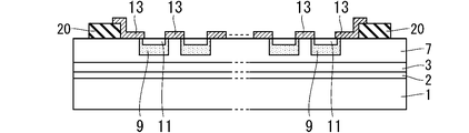
- FIG. 2 is a plan view schematically illustrating the configuration of the silicon carbide semiconductor device according to the present embodiment.
- 3 is a cross-sectional view corresponding to the cross section 901 in FIG.
- the silicon carbide semiconductor device is formed on an N-type SiC substrate 1, an N-type buffer layer 2 formed on the upper surface of the SiC substrate 1, and an upper surface of the buffer layer 2.
- Back gate region 9 source region 11 which is an N type diffusion layer partially formed in the surface layer of back gate region 9, and back gate region 9 sandwiched between source region 11 and drain region 7.
- a gate electrode 13 formed on the gate oxide film and a tetraethyl orthosilicate (ie, TEOS) oxide film 20 formed on the drain region 7 are provided thereon. That. In FIGS. 2 and 3, gate electrode 13 is formed to extend over TEOS oxide film 20.
- TEOS tetraethyl orthosilicate
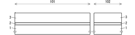
- FIG. 4 is a cross-sectional view illustrating a process until formation of an epitaxial layer in the silicon carbide semiconductor device according to the present embodiment.
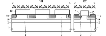
- FIG. 4 exemplifies a MOSFET region 101 which is a region in which a MOSFET is formed, and a mark region 102 which is a region in which a mark is arranged.
- N-type buffer layer 2 is grown on the upper surface of N-type SiC substrate 1, and N-type epitaxial layer 3 is further formed on the upper surface of buffer layer 2. Grow.
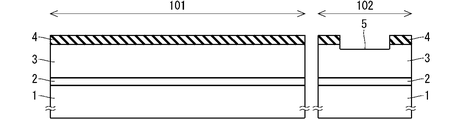
- FIG. 5 is a cross-sectional view illustrating the process until the mark is formed in the silicon carbide semiconductor device according to the present embodiment. Similarly, in FIG. 5, the MOSFET region 101 and the mark region 102 are illustrated.
- TEOS oxide film 4 is deposited on the upper surface of epitaxial layer 3. Then, the TEOS oxide film 4 in the mark area 102 is partially removed by photolithography. Further, the recess 5 is formed on the upper surface of the epitaxial layer 3 exposed by removing the TEOS oxide film 4 by dry etching. The recess 5 in the mark area 102 formed in this manner is a mark used for photolithography until the gate electrode 13 is formed.
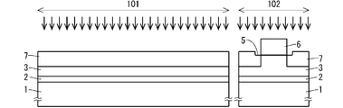
- FIG. 6 is a cross-sectional view illustrating the steps up to ion implantation when the drain region is formed in the silicon carbide semiconductor device according to the present embodiment. Similarly in FIG. 6, the MOSFET region 101 and the mark region 102 are illustrated.
- a resist is applied to the upper surface of the epitaxial layer 3 from which the TEOS oxide film 4 has been removed, and then photolithography is performed. At this time, when the mark of the resist mask is aligned with the recess 5 in the mark area 102 and the exposure is performed, the pattern 6 can be formed.
- the drain region 7 for reducing the resistance of the drain region is formed by implanting nitrogen or phosphorus, which is an N-type ion species, from the upper surface of the epitaxial layer 3.
- P-type ion species aluminum, boron or BF 2 are implanted into the drain region (i.e., the region outside TEOS oxide film 20 in FIG. 2) several tens to several hundreds of micrometers away from MOSFET region 101.
- a ring-shaped P-type diffusion layer (not shown here) is formed to improve the off breakdown voltage.
- FIG. 7 is a cross-sectional view illustrating the steps up to ion implantation when the back gate region is formed, in the silicon carbide semiconductor device according to the present embodiment. Similarly in FIG. 7, the MOSFET region 101 and the mark region 102 are illustrated.
- a resist is applied to the upper surface of the drain region 7 and photoengraving is performed using the recess 5 as a mark. Then, a pattern 8 is formed on the resist, and aluminum, boron or BF 2 which is a P-type ion species is implanted to form a back gate region 9 which is a P-type diffusion layer.
- the implantation of the P-type ion species may be performed multiple times by changing the implantation energy.
- FIG. 8 is a cross-sectional view illustrating the steps up to ion implantation when a P-type diffusion layer is formed in the silicon carbide semiconductor device according to the present embodiment. Similarly in FIG. 8, a MOSFET region 101 and a mark region 102 are illustrated.
- a resist is applied to the upper surface of the back gate region 9 and the upper surface of the drain region 7, and photoengraving is performed using the recess 5 as a mark. Then, a pattern 10 is formed in the resist, and rotational injection of P type ion species aluminum, boron or BF 2 is performed at an angle of more than 0 ° and 45 ° or less at an energy of 80 keV or less. A P type diffusion layer 19 is formed.
- the P type diffusion layer 19 can be formed shallow. That is, the depth of the P type diffusion layer 19 can be adjusted by the implantation angle.
- the implantation of the P-type ion species may be performed multiple times while changing the implantation angle and the implantation energy. Note that the energy is set to 80 keV or less even when ion implantation is performed a plurality of times. Further, when forming the pattern 10 in the resist, it is formed so as to extend to both ends of the back gate region 9.
- rotational implantation is an implantation method in which ions are implanted while being tilted with respect to the target surface while rotating about the normal line of the target surface to which ions are to be implanted.
- the P type diffusion layer 19 is formed, for example, 0.5 ⁇ m deeper than the source region 11 which is continuously implanted in a later step. And, when forming the P type diffusion layer 19 to such a depth, ion implantation at an energy of 100 keV or more is not required. Therefore, charging of the charge of the resist by the ion implantation and foaming do not occur.
- the carrier concentration of the P type diffusion layer 19 by ion implantation is approximately equal to the carrier concentration of the back gate region 9 which is a P type diffusion layer by ion implantation.
- FIG. 9 is a cross-sectional view illustrating the configuration in the case where the position of the pattern 10 is shifted with respect to the recess 5 as a mark at the time of photolithography.
- FIG. 10 is a cross-sectional view for illustrating the principle of the off breakdown voltage of the silicon carbide semiconductor device according to the present embodiment.
- P type diffusion layer 19 is formed asymmetrically with respect to back gate region 9.
- the P type diffusion layer 19 protrudes from the back gate region 9, in other words, the P type diffusion layer 19 is formed at a position in contact with the back gate region 9 and the drain region 7.
- a mask used in forming the N-type source region 11 can be used as a mask in forming the P-type diffusion layer 19, so another mask is newly added. There is no need to prepare Further, since the P type diffusion layer 19 can be formed to cover the N type source region 11 so as to be separated by a predetermined distance, the distance between the N type source region 11 and the drain region 7 is set to It can always be secured above a certain level. Thus, no withstand voltage failure occurs.
- FIG. 22 is a cross-sectional view illustrating another configuration where the position of the pattern 10 is shifted with respect to the recess 5 as a mark at the time of photolithography.
- P type diffusion layer 19 is formed asymmetrically with respect to back gate region 9.
- the distance between the P type diffusion layer 19 and the drain region 7 is different between the P type diffusion layer 19 and the left and right. Specifically, the spacing 557 on the right side of the P type diffusion layer 19 is smaller than the spacing 558 on the left side of the P type diffusion layer 19.
- the width 552 is larger than the width 552 overlapping the gate oxide film 12 of the back gate region 9 in plan view.
- the width 553 of the P type diffusion layer 19 overlapping in plan view with the gate oxide film 12 positioned on the left side is flat with the gate oxide film 12 of the back gate region 9. It has a width 554 or less overlapping in visual.
- the distance 504 between the drain region 7 and the source region 11 in the surface layer of the back gate region 9 is, for example, 0.4 ⁇ m or more and 0.6 ⁇ m or less.
- the distance 504 corresponds to the effective channel length.
- the recess 5 is used as a mark. If misalignment of the pattern 10 with respect to the mark occurs and the direction of the misalignment is different, the distance 504 in FIG. 10 can be, for example, 0.4 ⁇ m, which is the lower limit value.
- the distance 504 in FIG. 10 may be a length equal to or less than the lower limit.
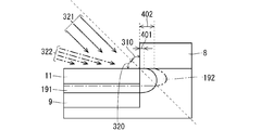
- FIG. 11 is a cross-sectional view illustrating a configuration in which ions are rotationally implanted at an angle larger than 45 °.
- FIG. 12 is a cross-sectional view illustrating the configuration in the case where ions are rotationally implanted at an angle of 45 ° or less.
- the angle 310 in FIG. 11 indicates 45 °
- the ion implantation 311 indicates, for example, a state of ion implantation in the case of rotational implantation at an angle of 80 ° larger than 45 °
- the P type diffusion layer 195 performs ion implantation.
- 11 shows a P type diffusion layer formed by 311.
- a distance 405 represents the distance between the source region 11 and the drain region 7 which is caused by the P type diffusion layer 195 formed by the ion implantation 311.
- the angle 320 in FIG. 12 indicates 45 °
- the ion implantation 321 indicates the state of ion implantation in the case of rotational implantation at an angle of 45 °, for example.
- the P type diffusion layer 191 is formed by the ion implantation 321 P-type diffusion layer.
- a distance 401 represents the distance between the source region 11 and the drain region 7 caused by the P type diffusion layer 191 formed by the ion implantation 321.
- ion implantation 322 in FIG. 12 shows, for example, a state of ion implantation in the case of rotational implantation at an angle of 10 ° which is 45 ° or less, and P type diffusion layer 192 is formed by ion implantation 322. Shows a diffusion layer of the type. Further, the distance 402 represents the distance between the source region 11 and the drain region 7 caused by the P type diffusion layer 192 formed by the ion implantation 322.
- the P type diffusion layer 195, the P type diffusion layer 191, and the P type diffusion layer 192 are formed respectively in the case where the ion implantation is performed and the case where the ions are rotationally implanted at an angle of 10 °, for example.
- the angle of the rotationally implanted ions with respect to the target plane is large. It can be seen that as the distance between the source region 11 and the drain region 7 decreases.
- the distance 504 between the source region 11 and the drain region 7 in FIG. 10 can be controlled by adjusting the angle of the rotationally implanted ions with respect to the target surface.
- the P type diffusion layer 19 can be formed in a good range by rotationally implanting ions in an angular range of 30 ° or more and 45 ° or less.
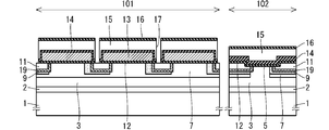
- the drain region 7 which is an N-type diffusion layer is formed on the upper surface of the N-type epitaxial layer 3 of SiC.
- the epitaxial layer 3 and the drain region 7 function as a drain region.
- a back gate region 9 which is a P-type diffusion layer is partially formed.
- a source region 11 which is an N-type diffusion layer is partially formed.
- the gate electrode 13 is formed via the gate oxide film 12.
- Source region 11 extends to gate electrode 13 in plan view.
- a TEOS oxide film 14 is formed to cover the gate electrode 13
- a borophosphosilicate glass (BPSG) film 15 is formed to cover the TEOS oxide film 14.
- a TEOS oxide film 16 is formed to cover the BPSG film 15.
- source electrode 18 is formed to cover TEOS oxide film 16 and source region 11.
- a strong electric field portion 500, a depletion layer 501 extending to the N-type diffusion layer side, and a depletion layer 502 extending to the P-type diffusion layer side are respectively shown.
- a distance 504 indicates the distance between the drain region 7 and the source region 11 in the surface layer of the back gate region 9.
- 0 V is applied to the source electrode 18 and the gate electrode 13 in FIG. 10, and a voltage is applied to the epitaxial layer 3 and the drain region 7.
- the depletion layer 501 extends on the N-type diffusion layer side
- the depletion layer 502 extends on the P-type diffusion layer side.
- depletion layer 501 and depletion layer 502 do not extend any more, and the electric field strength in strong electric field portion 500 becomes stronger. Then, an avalanche occurs in the strong electric field unit 500.
- the voltage value at that time is the off breakdown voltage.
- the depletion layer 502 reaches the source region 11 which is an N-type diffusion layer before the depletion layer 502 extending to the P-type diffusion layer side extends, a leak current is generated between the drain and the source at that time. , Off withstand voltage decreases. Therefore, when the distance 504 which is the distance between the drain region 7 and the source region 11 decreases, the margin of the depletion layer 502 decreases.
- P-type ion species are rotationally implanted at an angle of 45 ° or less while using the resist mask for forming the source region 11 as it is. Diffusion layer 19 is formed. Then, the distance 504 which is the distance between the source region 11 and the drain region 7 is larger than the width of the depletion layer extending to the P-type diffusion layer side by the P-type diffusion layer 19. Therefore, the decrease in off breakdown voltage can be suppressed.
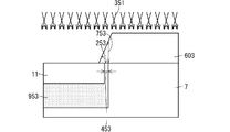
- FIG. 13 is a cross-sectional view in the case where the angle at the end of the resist for forming the P type diffusion layer and the source region is 30 °.
- FIG. 14 is a cross-sectional view in the case where the angle at the end of the resist for forming the P type diffusion layer and the source region is 45 °.
- FIG. 15 is a cross-sectional view in the case where the angle at the end of the resist for forming the P type diffusion layer and the source region is 80 °.
- the shape of the resist end after photoengraving is as a trapezoid 601, a trapezoid 602 and a trapezoid 603, ie, A tapered shape is formed at the resist end, P-type ion species are rotationally injected, and N-type ion species for forming the source region 11 are further implanted using the same resist.
- the manner in which P-type ion species are rotationally injected is shown as ion implantation 351.
- the source region is formed by the P type diffusion layer 951 formed by rotational injection of P type ion species.
- a distance 451 is generated between 11 and the drain region 7. Note that the P type diffusion layer 951 is formed immediately below the resist whose thickness is smaller than the thickness 751 of the resist through which the P type ion species penetrate by ion implantation.
- the P type diffusion layer 952 formed by rotational injection of P type ion species A distance 452 occurs between the source region 11 and the drain region 7.
- the P type diffusion layer 952 is formed immediately below the resist having a thickness smaller than the thickness 752 of the resist through which the P type ion species penetrates by ion implantation.
- the P type diffusion layer 953 formed by rotational injection of P type ion species A distance 453 is generated between the source region 11 and the drain region 7.
- the P-type diffusion layer 953 is formed immediately below the resist having a thickness smaller than the thickness 753 of the resist through which the P-type ion species penetrate by ion implantation.
- the angle of the resist edge is 30 °
- the angle of the resist edge is 45 ° when the angle 252 of the resist edge is 45 °
- the angle of the resist edge is 80 °. It can be seen that the distance between the source region 11 and the drain region 7 decreases as the distance increases.
- the distance between the drain region and the source region varies, and the off breakdown voltage of the MOSFET decreases.
- the distance between the drain region and the source region can be adjusted by controlling the inclination angle of the resist end. Since the exposure apparatus for forming the resist is configured to apply light perpendicularly to the resist, the shape of the resist end is formed substantially vertically. The method in which the resist is not provided with the inclination angle is preferable in that it can be formed more easily.
- FIG. 16 is a cross-sectional view illustrating the steps up to ion implantation when the source region is formed, in the silicon carbide semiconductor device according to the present embodiment. Similarly in FIG. 16, the MOSFET region 101 and the mark region 102 are illustrated.
- the source region 11 is formed shallower than the P type diffusion layer 19.
- the ion implantation for forming the source region 11 may be performed before forming the P type diffusion layer 19.
- FIG. 23 is a cross-sectional view illustrating the steps up to ion implantation when the source region is formed, in the silicon carbide semiconductor device according to the present embodiment.
- the configuration in FIG. 23 is formed using the same resist as the resist on which the P-type diffusion layer 19 formed asymmetrically as shown in FIG. 22 is formed. Therefore, the distance between the N-type source region 11 and the drain region 7 is different on the left and right of the N-type source region 11. Specifically, the spacing 559 on the right side of the N-type source region 11 is smaller than the spacing 560 on the left side of the N-type source region 11.
- the gap 559 is reduced, the impurity concentration of only the back gate region 9 which is a P type diffusion layer (as described in FIG. 10, the depletion layer extends from the drain region 7.
- the depletion layer is low
- the voltage reaches the N-type source region 11. As a result, withstand voltage failure occurs.
- the addition of the P-type diffusion layer 19 increases the total concentration of the P-type diffusion layer between the N-type source region 11 and the drain region 7, thereby suppressing the extension of the depletion layer. it can. Therefore, the withstand voltage does not decrease.
- annealing is performed at 1700 ° C. or higher to activate the drain region 7, the back gate region 9, the P type diffusion layer 19 and the source region 11.
- a carbon-based film such as a graphite film is formed and then the annealing process is performed. After the annealing process, the carbon-based film is removed (not shown here).
- a TEOS oxide film is deposited, for example, at 800 nm or more and 1500 nm or less on the upper surface of the drain region 7 to perform photolithography. Then, a field oxide film is formed by etching the TEOS oxide film (not shown here).
- FIG. 17 is a cross-sectional view illustrating the steps up to formation of the gate electrode in the silicon carbide semiconductor device according to the present embodiment. Also in FIG. 17, a MOSFET region 101 and a mark region 102 are illustrated.
- the upper surfaces of drain region 7, back gate region 9, P type diffusion layer 19 and source region 11 activated by annealing are oxidized, and have a thickness of, for example, 30 nm or more, and
- the gate oxide film 12 is formed to be 70 nm or less.
- N-type polysilicon is deposited on the upper surface of the gate oxide film 12 and photoengraving is further performed. Then, the gate electrode 13 is formed by dry etching polysilicon.
- gate oxide film 12 is the surface of back gate region 9 sandwiched between drain region 7 and source region 11, and the surface of P type diffusion layer 19 sandwiched between drain region 7 and source region 11. In contact with each other.
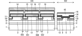
- FIG. 18 is a cross-sectional view illustrating a process until an interlayer oxide film is formed in the silicon carbide semiconductor device according to the present embodiment. Similarly in FIG. 18, the MOSFET region 101 and the mark region 102 are illustrated.
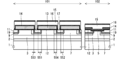
- FIG. 24 is a cross-sectional view illustrating a process until an interlayer oxide film is formed in the silicon carbide semiconductor device according to the present embodiment. Similarly in FIG. 24, the MOSFET region 101 and the mark region 102 are illustrated.
- FIG. 25 is a cross-sectional view illustrating a process until an interlayer oxide film is formed in the silicon carbide semiconductor device according to the present embodiment. Similarly in FIG. 25, the MOSFET region 101 and the mark region 102 are illustrated.
- the width 551 of the P type diffusion layer 19 overlapping in plan view with the gate oxide film 12 positioned on the right side is a back gate region.
- the width 552 is larger than the width 552 overlapping with the gate oxide film 12 of FIG.
- TEOS oxide film 14 is deposited to cover gate oxide film 12 and gate electrode 13, and BPSG film 15 is formed on the upper surface of TEOS oxide film 14, for example, 300 nm or more, Depot with a thickness of 1000 nm or less. Then, a TEOS oxide film 16 is again deposited on the upper surface of the BPSG film 15 to form an interlayer oxide film.
- FIG. 19 is a cross-sectional view illustrating the process until the contact is formed in the silicon carbide semiconductor device according to the present embodiment. Also in FIG. 19, the MOSFET region 101 and the mark region 102 are illustrated similarly.
- FIG. 26 is a cross-sectional view illustrating the process until the contact is formed in the silicon carbide semiconductor device according to the present embodiment. Similarly in FIG. 26, the MOSFET region 101 and the mark region 102 are illustrated.
- FIG. 27 is a cross-sectional view illustrating the process until the contact is formed in the silicon carbide semiconductor device according to the present embodiment. Similarly in FIG. 27, the MOSFET region 101 and the mark region 102 are illustrated.
- a resist is applied to the upper surface of the TEOS oxide film 16, and then photolithography is performed. Then, wet etching is performed, followed by dry etching to form a contact 17 as illustrated in FIG.
- the etching of the TEOS oxide film 16, the BPSG film 15, and the TEOS oxide film 14 at the time of contact formation may be dry etching only, or may be wet etching after dry etching.
- the pair of gate oxide films 12 sandwiching the contact 17 are in contact with part of the surface of the source region 11 respectively.
- the width 555 overlapping the gate oxide film 12 located on the right side with respect to the contact 17 of the source region 11 in plan view is the plan view with the gate oxide film 12 located on the left side with respect to the contact 17 of the source region 11. Larger than the overlapping width (see FIG. 27).
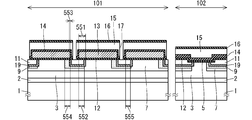
- FIG. 20 is a cross-sectional view illustrating a process until wiring is formed in the silicon carbide semiconductor device according to the present embodiment. Similarly in FIG. 20, a MOSFET region 101 and a mark region 102 are illustrated.
- FIG. 21 is also a cross-sectional view illustrating the step up to the formation of a wire in the silicon carbide semiconductor device according to the present embodiment. Similarly, in FIG. 21, the MOSFET region 101 and the mark region 102 are illustrated.
- Ni is sputtered to lower the contact resistance on the outermost surface, and then photolithography is performed. Then, Ni formed on the surface other than the source region 11 exposed after the contact formation is removed, and heat treatment is further performed to form NiSi (not shown here).
- FIG. 20 is a cross-sectional view illustrating a configuration in the case where a mask displacement occurs when forming the P type diffusion layer 19 by rotationally implanting ions at an angle of 45 °.
- the P type diffusion layer 19 is formed across the surface layer of the drain region 7 and the surface layer of the back gate region 9. In addition, the P type diffusion layer 19 is formed shallower than the back gate region 9.
- the width of the P type diffusion layer 19 overlapping with the gate oxide film 12 located on the right side with respect to the contact 17 in plan view is the gate oxide located on the left side with respect to the contact 17 of the P type diffusion layer 19.
- the width is larger than the overlapping width of the film 12 in plan view.
- the back gate region 9 which is a P type diffusion layer near the edge of the gate electrode 13 and the P type diffusion layer 19 have an asymmetrical shape. That is, the widths (that is, the widths 551 and 553) of the P type diffusion layer 19 overlapping in a plan view with the gate oxide film 12 are different on the left and right of the contact 17.
- the overlapping width with the gate oxide film 12 in plan view is the same on the left and right of the contact 17.
- FIG. 28, FIG. 29, FIG. 30, and FIG. 31 are cross-sectional views illustrating steps up to formation of interconnections in the silicon carbide semiconductor device according to the present embodiment.
- the back gate region 9, which is a P type diffusion layer, has different overlapping widths with the gate oxide film 12 in plan view. Specifically, the width 552 on the right side of the contact 17 is smaller than the width 554 on the left side of the contact 17.
- the P type diffusion layer 19 in which the source region 11 is formed and the back gate region 9 are formed asymmetrically. That is, the center of the P-type diffusion layer 19 in which the source region 11 is formed inside is shifted from the center of the back gate region 9 in the left-right direction.
- the width of the back gate region 9 on the left side of the P type diffusion layer 19 in which the source region 11 is formed inside is the back gate region 9 on the right side of the P type diffusion layer 19 in which the source region 11 is formed inside. Different from the width of
- the P type back gate region 9 hardly diffuses because it has a smaller diffusion coefficient than Si when ion implantation and annealing thereafter at 1700 ° C. for activation are performed. , The corner of the joint bottom is rounded. Similarly, when formed by ion implantation, the corner of the junction bottom of the P type diffusion layer 19 is also rounded.
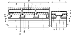
- FIG. 21 is a cross-sectional view illustrating a configuration in the case where no mask displacement occurs when forming the P type diffusion layer 19 by rotationally implanting ions at an angle of 45 °.
- the back gate region 9 and the P type diffusion layer 19 have a symmetrical shape. That is, the overlapping width of the P type diffusion layer 19 with the gate oxide film 12 in plan view is equal on the left and right of the contact 17.
- Whether the shape of the structure is symmetric or asymmetric can be discriminated from the dC / dV image of the cross section by, for example, scanning capacitance microscopy.
- scanning capacitance microscopy a profile close to the concentration distribution can be obtained as the carrier concentration distribution in the cross section.
- the P type diffusion layer 19 is not provided. Therefore, when the mask for forming the source region 11 is displaced from the mask for forming the back gate region 9, the source is not The region 11 may protrude from the back gate region 9 or the distance from the source region 11 to the back gate region 9 may be short.
- the source region 11 can be formed inside the P-type diffusion layer 19 by forming the P-type diffusion layer 19 by rotational implantation using a mask for forming the source region 11. Therefore, even when the source region 11 protrudes from the back gate region 9, the electrical characteristics of the semiconductor device can be maintained, and a sufficient distance from the source region 11 to the back gate region 9 can be secured.
- the P-type diffusion layer 19 is formed by rotational injection of ions at an angle of 45 ° or less, thereby providing a gate electrode Even if the source region 11 is asymmetrical, the distance between the source region 11 and the drain region 7 can be secured.
- the off breakdown voltage of the silicon carbide semiconductor device is determined by the depletion layer extending to the P type diffusion layer and the depletion layer extending to the N type diffusion layer, and according to the silicon carbide semiconductor device in the present embodiment This is because the depletion layer extending to the P type diffusion layer does not reach the N type diffusion layer of the source region before the occurrence of an avalanche at 500.
- the silicon carbide semiconductor device includes the silicon carbide semiconductor layer of the first conductivity type, the second diffusion layer of the second conductivity type, and the second of the second conductivity type. And a first gate insulating film, a second gate insulating film, a first gate electrode, and a second gate electrode.
- the silicon carbide semiconductor layer corresponds to, for example, buffer layer 2, epitaxial layer 3, and drain region 7.
- the second diffusion layer corresponds to, for example, the back gate region 9.
- the third diffusion layer corresponds to, for example, the P-type diffusion layer 19.
- the first gate insulating film and the second gate insulating film correspond to, for example, a pair of gate oxide films 12 sandwiching one contact 17 respectively.
- the first gate electrode and the second gate electrode correspond to, for example, a pair of gate electrodes 13 sandwiching one contact 17 respectively.
- the drain region 7 is formed on the surface layer of the epitaxial layer 3.
- the back gate region 9 is partially formed in the surface layer of the drain region 7.
- the P type diffusion layer 19 is formed across the surface layer of the drain region 7 and the surface layer of the back gate region 9.
- gate oxide film 12 located on the right side with respect to a certain contact 17 is formed in contact with a portion of the surface of back gate region 9 and a portion of the surface of P type diffusion layer 19 respectively.
- Ru In FIG. 20, gate oxide film 12 located on the left side with respect to a certain contact 17 contacts another portion of the surface of back gate region 9 and the other portion of the surface of P type diffusion layer 19 respectively.
- gate electrode 13 positioned on the right side with respect to a certain contact 17 is formed in contact with gate oxide film 12 positioned on the right side with respect to certain contact 17 as well.
- gate electrode 13 located on the left side with respect to a certain contact 17 is formed in contact with gate oxide film 12 located on the left side with respect to certain contact 17 as well.
- the P type diffusion layer 19 is formed shallower than the back gate region 9.
- the width of the P type diffusion layer 19 overlapping with the gate oxide film 12 located on the right side with respect to the certain contact 17 in plan view is located on the left side with respect to the certain contact 17 of the P type diffusion layer 19. The width is larger than the overlapping width with the gate oxide film 12 in plan view.
- the silicon carbide semiconductor device includes the silicon carbide semiconductor layer of the first conductivity type, the second diffusion layer of the second conductivity type, and the second conductivity type.
- a third diffusion layer, a first gate insulating film, and a first gate electrode
- the silicon carbide semiconductor layer corresponds to, for example, buffer layer 2, epitaxial layer 3, and drain region 7.
- the second diffusion layer corresponds to, for example, the back gate region 9.
- the third diffusion layer corresponds to, for example, the P-type diffusion layer 19.
- the first gate insulating film corresponds to, for example, the gate oxide film 12 sandwiching one contact 17.
- the first gate electrode corresponds to, for example, the gate electrodes 13 sandwiching one contact 17.
- the drain region 7 is formed on the surface layer of the epitaxial layer 3.
- the back gate region 9 is partially formed in the surface layer of the drain region 7.
- the P type diffusion layer 19 is formed at a position in contact with the drain region 7 and the back gate region 9.
- gate oxide film 12 located on the right side with respect to a certain contact 17 is formed in contact with a portion of the surface of back gate region 9 and a portion of the surface of P type diffusion layer 19 respectively.
- Ru In FIG. 20, gate oxide film 12 located on the left side with respect to a certain contact 17 contacts another portion of the surface of back gate region 9 and the other portion of the surface of P type diffusion layer 19 respectively. It is formed.
- gate electrode 13 positioned on the right side with respect to a certain contact 17 is formed in contact with gate oxide film 12 positioned on the right side with respect to certain contact 17 as well.
- gate electrode 13 located on the left side with respect to a certain contact 17 is formed in contact with gate oxide film 12 located on the left side with respect to certain contact 17 as well.
- the width of the P type diffusion layer 19 overlapping with the gate oxide film 12 positioned on the right side with respect to the certain contact 17 in plan view is the same as that of the back gate region 9.
- the width is larger than the overlapping width with the gate oxide film 12 in plan view.
- the overlapping width of the P type diffusion layer 19 with the gate oxide film 12 located on the left side with respect to a certain contact 17 in plan view is less than the width overlapping with the gate oxide film 12 of the back gate region 9 in plan view. is there.
- the distance between source region 11 and drain region 7 is secured by P type diffusion layer 19 formed to extend out from back gate region 9, so the off breakdown voltage of the silicon carbide semiconductor device Can be suppressed.
- the silicon carbide semiconductor device includes the first diffusion type fourth diffusion layer formed partially in the surface layer of the P type diffusion layer 19.
- the fourth diffusion layer corresponds to, for example, the source region 11.
- Gate oxide film 12 is formed at least on the surface of back gate region 9 sandwiched between drain region 7 and source region 11 and on the surface of P type diffusion layer 19 sandwiched between drain region 7 and source region 11. They are formed in contact with each other. According to such a configuration, since the distance between source region 11 and drain region 7 is secured by P type diffusion layer 19, it is possible to suppress a decrease in off breakdown voltage of the silicon carbide semiconductor device.
- the gate oxide film 12 located on the right side with respect to a certain contact 17 is formed in contact with a part of the surface of the source region 11. Further, gate oxide film 12 located on the left side with respect to a certain contact 17 is formed in contact with another part of the surface of source region 11.
- the overlapping width of the source region 11 with the gate oxide film 12 positioned on the right side with respect to the certain contact 17 in plan view is the same as that of the gate oxide film 12 located on the left side with respect to the certain contact 17 Larger than the overlapping width in vision. According to such a configuration, since the distance between source region 11 and drain region 7 is secured by P type diffusion layer 19, it is possible to suppress a decrease in off breakdown voltage of the silicon carbide semiconductor device.
- P-type diffusion sandwiched between drain region 7 and source region 11 overlaps in plan view with gate oxide film 12 positioned on the right side with respect to a certain contact 17
- the width of layer 19 is less than 1.0 ⁇ m. According to such a configuration, since the silicon carbide semiconductor device having an effective channel length of less than 1.0 ⁇ m can be manufactured, the characteristics of the silicon carbide semiconductor device can be improved.
- the drain region 7 of the first conductivity type is formed on the surface of the epitaxial layer 3 of the first conductivity type by ion implantation. .
- a back gate region 9 of the second conductivity type is partially formed by ion implantation.
- a resist pattern is formed on the surface of the back gate region 9.
- the resist pattern corresponds to, for example, the pattern 10.
- the second conductivity type P-type diffusion layer 19 is formed by rotational implantation of ions at an angle of 45 ° or less across the surface layer of the drain region 7 and the surface layer of the back gate region 9 in the state exposed from the pattern 10.
- the source region 11 of the first conductivity type is partially formed by ion implantation in the surface layer of at least the back gate region 9 in the state of being exposed from the pattern 10. Then, at least on the surface of the back gate region 9 sandwiched between the drain region 7 and the source region 11 and on the surface of the P type diffusion layer 19 sandwiched between the drain region 7 and the source region 11 A gate insulating film and a second gate insulating film are formed.
- the first gate insulating film and the second gate insulating film correspond to, for example, the gate oxide film 12.
- the gate electrode 13 is formed on the surface of the gate oxide film 12 respectively.
- the P type diffusion layer 19 is formed shallower than the back gate region 9.
- the source region 11 is partially formed in the surface layer of the P type diffusion layer 19.
- the width of the P type diffusion layer 19 overlapping with the gate oxide film 12 located on the right side with respect to the certain contact 17 in plan view is located on the left side with respect to the certain contact 17 of the P type diffusion layer 19.
- the width is larger than the overlapping width with the gate oxide film 12 in plan view.
- the source region 11 even when the formation position of the source region 11 deviates from the formation position of the back gate region 9 and the distance between the source region 11 and the drain region 7 becomes small, the source region The distance between the source region 11 and the drain region 7 is secured by the P type diffusion layer 19 formed by rotational implantation while using the same resist pattern as that of the resist pattern 11. Therefore, it is possible to suppress a drop in the off breakdown voltage of the silicon carbide semiconductor device. Therefore, the yield is improved.
- the P type diffusion layer 19 is formed by rotational implantation of ions at an angle of 30 ° or more and 45 ° or less. According to such a configuration, the distance between the source region 11 and the drain region 7 is sufficiently secured by the P type diffusion layer 19 formed by rotational implantation of ions in the angle range. Therefore, it is possible to suppress a drop in the off breakdown voltage of the silicon carbide semiconductor device.
- the end of the pattern 10 is tapered. According to such a configuration, since the formation range of the P type diffusion layer 19 can be controlled by the tapered shape, a sufficient distance between the source region 11 and the drain region 7 is secured.
- each component in the embodiments described above is a conceptual unit, and within the scope of the technology disclosed in the present specification, one component is composed of a plurality of structures. , A case where one component corresponds to a part of a structure, and a case where a plurality of components are provided in one structure.
- each component in the embodiment described above includes a structure having another structure or shape as long as the same function is exhibited.
- the material when a material name or the like is described without being specified, unless the contradiction arises, the material includes other additives, for example, an alloy or the like. Shall be included.
- the semiconductor substrate is N-type, but may be P-type. That is, although the MOSFET is described as an example of a silicon carbide semiconductor device in the embodiment described above, an example of a silicon carbide semiconductor device is an insulated gate bipolar transistor (i.e., an IGBT) Cases can also be assumed.
- MOSFET is described as an example of a silicon carbide semiconductor device in the embodiment described above, an example of a silicon carbide semiconductor device is an insulated gate bipolar transistor (i.e., an IGBT) Cases can also be assumed.
- the source electrode corresponds to the emitter electrode
- the drain electrode corresponds to the collector electrode.
- a layer of a conductivity type opposite to the drift layer is located on the lower surface of the drift layer, but the layer located on the lower surface of the drift layer is the lower surface of the drift layer. It may be a layer newly formed, or may be a semiconductor substrate on which a drift layer is formed as in the embodiments described above.
- Reference Signs List 1 SiC substrate, 2 buffer layer, 3 epitaxial layer, 4, 14, 16, 20 TEOS oxide film, 5 recess, 6, 8, 10 pattern, 7 drain region, 9 back gate region, 11 source region, 12 gate oxide film , 13 gate electrodes, 15 BPSG films, 17 contacts, 18 source electrodes, 19, 191, 192, 195, 951, 952, 953 diffusion layers, 101, 801 MOSFET regions, 102, 803 mark regions, 251, 252, 253, 310, 320 angles, 311, 321, 322, 351 ion implantation, 401, 402, 405, 451, 452, 453, 504 distance, 500 strong electric field part, 501, 502 depletion layer, 551, 552, 553, 554, 555 Width, 557, 558, 559, 5 0 interval, 601, 602 trapezoid, 751,752,753 thickness, 802 scribe region 901 section.
Landscapes
- Electrodes Of Semiconductors (AREA)
- Insulated Gate Type Field-Effect Transistor (AREA)
- Chemical & Material Sciences (AREA)
- Crystallography & Structural Chemistry (AREA)
Abstract
Selon la présente invention, un dispositif à semi-conducteurs au carbure de silicium est produit sans abaisser la tension de claquage en état d'arrêt. Un dispositif à semi-conducteurs au carbure de silicium selon la présente invention comprend : une deuxième couche de diffusion (9) d'un second type de conductivité, qui est partiellement formée dans la couche superficielle de couches semi-conductrices de carbure de silicium (2, 3, 7) d'un premier type de conductivité ; une troisième couche de diffusion (19) du second type de conductivité, qui est formée dans au moins une partie de la couche superficielle de la deuxième couche de diffusion ; et une quatrième couche de diffusion (11) du premier type de conductivité, qui est partiellement formée dans la couche superficielle de la troisième couche de diffusion. La troisième couche de diffusion est formée de manière à être moins profonde que la deuxième couche de diffusion ; la quatrième couche de diffusion est formée dans la troisième couche de diffusion lorsqu'elle est vue en coupe transversale ; et la troisième couche de diffusion est asymétrique par rapport à la deuxième couche de diffusion.
Priority Applications (4)
| Application Number | Priority Date | Filing Date | Title |
|---|---|---|---|
| CN201880071922.8A CN111316406A (zh) | 2017-11-13 | 2018-11-09 | 碳化硅半导体装置以及碳化硅半导体装置的制造方法 |
| US16/651,222 US20200279947A1 (en) | 2017-11-13 | 2018-11-09 | Silicon carbide semiconductor device and method of manufacturing silicon carbide semiconductor device |
| DE112018005451.9T DE112018005451T5 (de) | 2017-11-13 | 2018-11-09 | Siliciumcarbid-halbleitereinheit und verfahren zur herstellung einer siliciumcarbid-halbleitereinheit |
| JP2019552397A JP6746010B2 (ja) | 2017-11-13 | 2018-11-09 | 炭化珪素半導体装置、および、炭化珪素半導体装置の製造方法 |
Applications Claiming Priority (2)
| Application Number | Priority Date | Filing Date | Title |
|---|---|---|---|
| JP2017-218380 | 2017-11-13 | ||
| JP2017218380 | 2017-11-13 |
Publications (1)
| Publication Number | Publication Date |
|---|---|
| WO2019093465A1 true WO2019093465A1 (fr) | 2019-05-16 |
Family
ID=66439287
Family Applications (1)
| Application Number | Title | Priority Date | Filing Date |
|---|---|---|---|
| PCT/JP2018/041633 Ceased WO2019093465A1 (fr) | 2017-11-13 | 2018-11-09 | Dispositif à semi-conducteurs au carbure de silicium et procédé de fabrication de dispositif à semi-conducteurs au carbure de silicium |
Country Status (5)
| Country | Link |
|---|---|
| US (1) | US20200279947A1 (fr) |
| JP (1) | JP6746010B2 (fr) |
| CN (1) | CN111316406A (fr) |
| DE (1) | DE112018005451T5 (fr) |
| WO (1) | WO2019093465A1 (fr) |
Cited By (1)
| Publication number | Priority date | Publication date | Assignee | Title |
|---|---|---|---|---|
| JP2024526521A (ja) * | 2022-11-14 | 2024-07-19 | エシュウ セミコンダクター マニュファクチュアリング エレクトロニクス(シャオシン)コーポレーション | Mosfetデバイス及びその製造方法 |
Families Citing this family (1)
| Publication number | Priority date | Publication date | Assignee | Title |
|---|---|---|---|---|
| CN116364758B (zh) * | 2023-03-30 | 2023-11-14 | 苏州龙驰半导体科技有限公司 | SiC MOS器件 |
Citations (8)
| Publication number | Priority date | Publication date | Assignee | Title |
|---|---|---|---|---|
| JP2000514604A (ja) * | 1996-07-11 | 2000-10-31 | エービービー リサーチ リミテッド | 電圧制御半導体装置のためのSiC層中にチャンネル領域層を形成する方法 |
| JP2004207492A (ja) * | 2002-12-25 | 2004-07-22 | Mitsubishi Electric Corp | 半導体素子の製造方法 |
| JP2004319964A (ja) * | 2003-03-28 | 2004-11-11 | Mitsubishi Electric Corp | 半導体装置及びその製造方法 |
| JP2004363515A (ja) * | 2003-06-09 | 2004-12-24 | Mitsubishi Electric Corp | 炭化珪素半導体装置の製造方法 |
| US20160141412A1 (en) * | 2014-11-19 | 2016-05-19 | Hestia Power Inc. | Silicon carbide semiconductor device and method of manufacture thereof |
| WO2016084141A1 (fr) * | 2014-11-26 | 2016-06-02 | 株式会社日立製作所 | Élément de commutation à semi-conducteur et procédé de fabrication de dispositif à semi-conducteur au carbure de silicium |
| WO2016104264A1 (fr) * | 2014-12-25 | 2016-06-30 | 富士電機株式会社 | Dispositif à semi-conducteurs |
| WO2017081935A1 (fr) * | 2015-11-12 | 2017-05-18 | 三菱電機株式会社 | Dispositif à semi-conducteur au carbure de silicium et procédé de fabrication de dispositif à semi-conducteur au carbure de silicium |
Family Cites Families (8)
| Publication number | Priority date | Publication date | Assignee | Title |
|---|---|---|---|---|
| JP4848607B2 (ja) * | 2001-09-11 | 2011-12-28 | 株式会社デンソー | 炭化珪素半導体装置の製造方法 |
| JP3617507B2 (ja) | 2002-07-01 | 2005-02-09 | 日産自動車株式会社 | 炭化珪素半導体装置の製造方法、及びその製造方法によって製造される炭化珪素半導体装置 |
| JP4773169B2 (ja) * | 2005-09-14 | 2011-09-14 | エルピーダメモリ株式会社 | 半導体装置の製造方法 |
| JP4675813B2 (ja) * | 2006-03-31 | 2011-04-27 | Okiセミコンダクタ株式会社 | 半導体記憶装置およびその製造方法 |
| JP5098214B2 (ja) * | 2006-04-28 | 2012-12-12 | 日産自動車株式会社 | 半導体装置およびその製造方法 |
| JP5452062B2 (ja) * | 2009-04-08 | 2014-03-26 | 三菱電機株式会社 | 炭化珪素半導体装置の製造方法 |
| JP5716591B2 (ja) * | 2011-07-26 | 2015-05-13 | 三菱電機株式会社 | 半導体装置 |
| JP5936513B2 (ja) * | 2012-10-12 | 2016-06-22 | 三菱電機株式会社 | 横型高耐圧トランジスタの製造方法 |
-
2018
- 2018-11-09 WO PCT/JP2018/041633 patent/WO2019093465A1/fr not_active Ceased
- 2018-11-09 US US16/651,222 patent/US20200279947A1/en not_active Abandoned
- 2018-11-09 DE DE112018005451.9T patent/DE112018005451T5/de not_active Withdrawn
- 2018-11-09 JP JP2019552397A patent/JP6746010B2/ja active Active
- 2018-11-09 CN CN201880071922.8A patent/CN111316406A/zh active Pending
Patent Citations (8)
| Publication number | Priority date | Publication date | Assignee | Title |
|---|---|---|---|---|
| JP2000514604A (ja) * | 1996-07-11 | 2000-10-31 | エービービー リサーチ リミテッド | 電圧制御半導体装置のためのSiC層中にチャンネル領域層を形成する方法 |
| JP2004207492A (ja) * | 2002-12-25 | 2004-07-22 | Mitsubishi Electric Corp | 半導体素子の製造方法 |
| JP2004319964A (ja) * | 2003-03-28 | 2004-11-11 | Mitsubishi Electric Corp | 半導体装置及びその製造方法 |
| JP2004363515A (ja) * | 2003-06-09 | 2004-12-24 | Mitsubishi Electric Corp | 炭化珪素半導体装置の製造方法 |
| US20160141412A1 (en) * | 2014-11-19 | 2016-05-19 | Hestia Power Inc. | Silicon carbide semiconductor device and method of manufacture thereof |
| WO2016084141A1 (fr) * | 2014-11-26 | 2016-06-02 | 株式会社日立製作所 | Élément de commutation à semi-conducteur et procédé de fabrication de dispositif à semi-conducteur au carbure de silicium |
| WO2016104264A1 (fr) * | 2014-12-25 | 2016-06-30 | 富士電機株式会社 | Dispositif à semi-conducteurs |
| WO2017081935A1 (fr) * | 2015-11-12 | 2017-05-18 | 三菱電機株式会社 | Dispositif à semi-conducteur au carbure de silicium et procédé de fabrication de dispositif à semi-conducteur au carbure de silicium |
Cited By (2)
| Publication number | Priority date | Publication date | Assignee | Title |
|---|---|---|---|---|
| JP2024526521A (ja) * | 2022-11-14 | 2024-07-19 | エシュウ セミコンダクター マニュファクチュアリング エレクトロニクス(シャオシン)コーポレーション | Mosfetデバイス及びその製造方法 |
| JP7717188B2 (ja) | 2022-11-14 | 2025-08-01 | ユナイテッド ノバ テクノロジー - エシュウ(シャオシン)コーポレーション | Mosfetデバイス及びその製造方法 |
Also Published As
| Publication number | Publication date |
|---|---|
| JP6746010B2 (ja) | 2020-08-26 |
| DE112018005451T5 (de) | 2020-07-30 |
| JPWO2019093465A1 (ja) | 2020-04-23 |
| CN111316406A (zh) | 2020-06-19 |
| US20200279947A1 (en) | 2020-09-03 |
Similar Documents
| Publication | Publication Date | Title |
|---|---|---|
| US9466700B2 (en) | Semiconductor device and method of fabricating same | |
| CN105264667B (zh) | 碳化硅半导体装置及其制造方法 | |
| US12148824B2 (en) | MOSFET device with shielding region and manufacturing method thereof | |
| US10236341B2 (en) | Semiconductor device and method for manufacturing the same | |
| CN105590962A (zh) | 碳化硅半导体装置和用于制造碳化硅半导体装置的方法 | |
| KR101206382B1 (ko) | 반도체장치 및 반도체장치의 제조방법 | |
| TWI515893B (zh) | 垂直式功率金氧半場效電晶體與其形成方法 | |
| US8552492B2 (en) | Semiconductor device | |
| JP5583846B2 (ja) | 半導体装置 | |
| TWI841999B (zh) | 具有多重場板之高壓元件及其製造方法 | |
| US9666485B2 (en) | Method for forming semiconductor device having super-junction structures | |
| US7649222B2 (en) | Semiconductor device | |
| US9947750B2 (en) | Silicon carbide semiconductor switching device and method of manufacturing silicon carbide semiconductor switching device | |
| KR102062050B1 (ko) | 결합된 게이트 트렌치 및 컨택 에칭 프로세스 및 그와 관련된 구조체 | |
| CN111370486A (zh) | 沟槽型mos场效应晶体管及方法、电子设备 | |
| JP6746010B2 (ja) | 炭化珪素半導体装置、および、炭化珪素半導体装置の製造方法 | |
| US20200266295A1 (en) | High voltage ldmos transistor and methods for manufacturing the same | |
| US7923330B2 (en) | Method for manufacturing a semiconductor device | |
| KR102572194B1 (ko) | 반도체 소자 및 그의 제조 방법 | |
| US10008594B2 (en) | High voltage semiconductor device | |
| CN112531026A (zh) | 横向扩散金属氧化物半导体器件及其制造方法 | |
| US20170077227A1 (en) | Needle Field Plate MOSFET with Mesa Contacts and Conductive Posts | |
| JP7794725B2 (ja) | 半導体装置の製造方法 | |
| KR102251761B1 (ko) | 전력 반도체 소자 | |
| CN121692690A (zh) | 一种ldmos的制备方法及ldmos器件 |
Legal Events
| Date | Code | Title | Description |
|---|---|---|---|
| 121 | Ep: the epo has been informed by wipo that ep was designated in this application |
Ref document number: 18876311 Country of ref document: EP Kind code of ref document: A1 |
|
| ENP | Entry into the national phase |
Ref document number: 2019552397 Country of ref document: JP Kind code of ref document: A |
|
| 122 | Ep: pct application non-entry in european phase |
Ref document number: 18876311 Country of ref document: EP Kind code of ref document: A1 |