WO2016110968A1 - Dispositif programmable, appareil de commande utilisant ce dernier et procédé de contre-mesure en cas de défaillance - Google Patents
Dispositif programmable, appareil de commande utilisant ce dernier et procédé de contre-mesure en cas de défaillance Download PDFInfo
- Publication number
- WO2016110968A1 WO2016110968A1 PCT/JP2015/050283 JP2015050283W WO2016110968A1 WO 2016110968 A1 WO2016110968 A1 WO 2016110968A1 JP 2015050283 W JP2015050283 W JP 2015050283W WO 2016110968 A1 WO2016110968 A1 WO 2016110968A1
- Authority
- WO
- WIPO (PCT)
- Prior art keywords
- programmable device
- unit
- output
- configuration
- circuit area
- Prior art date
- Legal status (The legal status is an assumption and is not a legal conclusion. Google has not performed a legal analysis and makes no representation as to the accuracy of the status listed.)
- Ceased
Links
Images


Classifications
-
- H—ELECTRICITY
- H03—ELECTRONIC CIRCUITRY
- H03K—PULSE TECHNIQUE
- H03K19/00—Logic circuits, i.e. having at least two inputs acting on one output; Inverting circuits
- H03K19/02—Logic circuits, i.e. having at least two inputs acting on one output; Inverting circuits using specified components
- H03K19/173—Logic circuits, i.e. having at least two inputs acting on one output; Inverting circuits using specified components using elementary logic circuits as components
Definitions
- the present invention relates to a programmable device and a control device using the programmable device, and relates to a countermeasure for the failure.
- Programmable devices are frequently used as control LSIs for various electronic system devices, and in particular, the use of FPGA (Field Programmable Gate Array) is increasing.
- the FPGA stores logic circuit information in a memory (hereinafter referred to as configuration memory, CRAM) inside the device to construct an arithmetic circuit and a control circuit. By rewriting the contents of the CRAM, another logic circuit is immediately created. It can be changed to
- Patent Document 1 states that “a power-on reset circuit that sends a reset signal within a first time after power-on, and that power-on is monitored and the power is turned on after the first time has elapsed.
- a power supply monitoring circuit that outputs a signal indicating a signal, a system controller detection circuit that determines whether or not it is a system controller, and a field programmable gate array that completes configuration within a second time longer than the first time.
- a signal for determining that it is a system controller and a bus grant output signal connected in a daisy chain are forcibly fixed at least from the start of operation of the power-on reset circuit to the first time, It is controlled by the field programmable gate array after the second time has elapsed. It has been described as M E System Controller ".
- the problem of the soft error caused by this has become obvious particularly in the SRAM, logic gate, clock system and the like.
- the following are known as soft error mechanisms. That is, when neutrons with extremely high energy enter the nuclei constituting the device, nucleons (neutrons and protons) in the nucleus repeatedly collide, and nucleons with particularly high energy are emitted outside the nucleus.
- nucleon When the nucleon is unable to have enough kinetic energy to jump out of the nucleus, light particles such as protons, neutrons, deuterons, and alpha particles evaporate from the residual nuclei in the excited state.
- all of these secondary particles will fly in the distance device corresponding to the range.
- FPGA CRAMs are composed of SRAMs, and circuit information is destroyed due to soft errors caused by environmental radiation, which may cause malfunction of electronic system devices.
- electronic system devices that control social infrastructure may cause safety problems.
- countermeasures are taken using a plurality of components and devices so that the electronic system device is not affected by malfunctions, but this causes an increase in power consumption, development, verification man-hours, cost, and the like.
- Patent Document 1 The technology disclosed in Patent Document 1 is for a programmable device connected by a bus to prevent other devices from affecting unstable operations due to power supply noise or the like while writing circuit information to the CRAM memory immediately after power-on.
- the output of the programmable device is fixed by a logical mask. This is irrelevant to the destruction of the information in the CRAM of the programmable device, and does not exclude the influence due to the malfunction at the time of a soft error.
- An object of the present invention is not to make the operation of the electronic system apparatus a dangerous failure due to a failure occurring in the CRAM of the programmable device.
- the improvement of the safety of the electronic system apparatus is realized with low power consumption and low cost.
- the present application includes a plurality of means for solving the above-described problems.
- a programmable device having a configuration memory, an error detection unit for detecting a data reversal failure in the configuration memory, and a configuration
- a control unit that controls reading and writing of the memory the configuration memory has an output circuit area that stores circuit information that controls the output signal of the programmable device, and the control unit receives from the error detection unit.
- the configuration data is read from the safety data storage unit that stores the configuration data for fixing the output signal level of the programmable device, and is overwritten in the output circuit area.
- FIG. 1 is a configuration diagram of a programmable device according to Embodiment 1.
- FIG. 3 is a processing flow according to the first embodiment.
- FIG. 3 is a circuit configuration diagram of an output circuit region of the programmable device according to the first embodiment.
- FIG. 3 is a configuration diagram of an output circuit area overwrite control unit according to the first embodiment.
- FIG. 6 is an operation sequence diagram of the output circuit area overwrite control unit according to the first embodiment. It is a block diagram of the safety data which concerns on Example 2.
- FIG. FIG. 10 is a configuration diagram illustrating an output circuit region portion according to a third embodiment.
- FIG. 10 is a configuration diagram of a programmable device according to a fourth embodiment. 10 is a configuration diagram of a programmable device according to Embodiment 5.
- FIG. 10 is a configuration diagram illustrating an output circuit region portion according to a third embodiment.
- FIG. 10 is a configuration diagram of a programmable device according to Embodiment 9.
- FIG. 10 is a block diagram of the control apparatus carrying the programmable device which concerns on Example 10.
- FIG. It is a block diagram of the vehicle-mounted control apparatus carrying the programmable device which concerns on Example 11.
- FIG. It is a block diagram of the motor control part carrying the programmable device which concerns on Example 12.
- FIG. 15 is a configuration diagram of a robot equipped with a programmable device according to Example 13; It is a block diagram of the construction machine carrying the programmable device which concerns on Example 14.
- FIG. 10 is a configuration diagram of a programmable device according to Embodiment 9.
- FIG. It is a block diagram of the control apparatus carrying the programmable device which concerns on Example 10.
- FIG. It is a block diagram of the vehicle-mounted control apparatus carrying the programmable device which concerns on Example 11.
- FIG. It is a block diagram of the motor control part carrying the programmable device which concerns on Example 12.
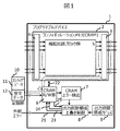
- FIG. 1 is a configuration diagram of the programmable device of this embodiment.
- the programmable device 1 includes a configuration memory (CRAM) 2 having logic circuit data for realizing a desired function as user logic.
- the functional circuit block group 5 that stores logic circuit information
- the programmable device 1 includes a CRAM R / W control unit 6 that controls access to data in the CRAM 2 and reads and writes to the CRAM, and a CRAM error detection unit 7 that determines whether there is an error in the data in the CRAM 2. Yes.
- a CRC (Cyclic Redundancy Code) code for error detection is added to the logic circuit data in the CRAM 2, and the entire CRAM 2 is read and read to perform error determination. It has a function.
- the programmable device 1 has an output circuit area overwrite control section 8 and an output circuit area address holding section 9 for storing and holding the address of the output circuit area.
- the external storage unit 10 is configured to fix the configuration data 11 that is circuit information that defines the function of the programmable device 1 and the output signal level of the area 3 in which the signal level of the output pin of the programmable device 1 can be set.
- Data 12 is stored.
- the safety data 12 is configuration data for fixing the output signal level, and is configuration data for forcibly fixing the circuit structure to the output, but defines the function of the programmable device 1. In order to distinguish it from the configuration data 11 which is circuit information, it is called safety data in this embodiment.
- the configuration data 11 and the safety data 12 may be stored in physically different devices.
- the CRAM error detector 7 detects data inversion due to factors such as environmental radiation of the CRAM, and then outputs the error detection signal to the output circuit area overwrite controller 8 as a trigger.
- the output circuit area overwrite control unit 8 obtains the address of the area 3 in which the signal level of the output pin that is the output circuit area of the programmable device 1 can be set from the output circuit area address holding unit 9 that stores and holds the address of the output circuit area. Then, the address is sent to the CRAM / R / W control unit 6 (24). At the same time, the storage area address and data size of the safety data 12 for fixing the output signal level in the external storage unit 10 are sent to the CRAM R / W control unit 6 (23).
- the storage address of the safety data 12 may be held by the CRAM / R / W control unit 6.
- the CRAM R / W control unit 6 reads the safety data 12 according to the received address, and writes it in the area 3 where the signal level of the output pin in the CRAM can be set. When the write process is completed, a completion signal is sent (25).
- the output circuit area address holding unit 9 holds the address of the area 4 that holds the setting of the input pin of the programmable device 1, and the safety for the area 4 that holds the setting of the input pin through the output circuit area overwriting control unit 8. Input can also be blocked by writing data.
- Fig. 2 shows the control procedure of the components of this embodiment.
- the programmable device 1 starts operation (31), and the CRAM error detection unit 7 monitors the presence / absence of an error in the CRAM 2 via the CRAM / R / W control unit 6 as described above. Detection is performed (32) (33). If there is no error (33b), error monitoring is continued, and if an error is detected (33a), an error detection signal is output from the CRAM error detector 7 (34).
- the output circuit area overwrite control unit 8 sends an instruction to read the safety data 12 to the CRAM / R / W control unit 6 (35).
- the output circuit area overwrite control unit 8 acquires the address of the area 3 where the signal level of the output pin of the programmable device 1 can be set from the output circuit area address holding unit 9 that stores and holds the output circuit area, and the address is stored in the CRAM.
- the data is sent to the R / W control unit 6 (36).
- the safety data 12 is written in the area 3 where the signal level of the output pin in the CRAM can be set (37).
- FIG. 3 shows a specific circuit configuration example of the area 3 in which the signal level of the output pin, which is the output circuit area in the CRAM, can be set.
- This area is composed of output pin blocks 41 connected to each output pin.
- Each output pin block 41 includes a flip-flop 42 which is a temporary data holding mechanism and a device side input to the flip-flop 42.
- the signal 44, the external signal 43, and the setting register 45 that stores the input / output of the external signal 43, the initial value of the flip-flop 42, the input / output direction, the signal potential level, and the like.
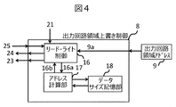
- FIG. 4 shows a circuit configuration example of the output circuit area overwrite control unit 8.
- the output circuit area overwrite control unit 8 includes a read / write control unit 16 that performs input / output processing of the area address, a data size storage unit 18 that holds the starting address and data size of the safety data 12, and a storage location of the safety data 12
- the address calculation unit 17 generates an address.
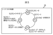
- FIG. 5 shows a state transition diagram of the read / write control unit 16 that performs the main sequence control among the components shown in FIG. In FIG. 5, it waits in P0 which is an idle state waiting for an error detection signal from the start of operation.
- P0 an idle state waiting for an error detection signal from the start of operation.
- an external error signal 21 that is a trigger signal or an error detection signal from the CRAM error detection unit 7
- the process moves to the state P1 and issues a calculation start instruction (16a) to the address calculation unit 17.
- the process moves to the state P2 and the storage address of the safety data 12 is received (16b).
- the CRAM R / W control unit 6 starts access to the external storage unit 10 and waits for a signal (25) notifying that the input of the safety data 12 has started.
- the process moves to the state P3, issues a safety data overwrite instruction (24) to the CRAM, and when writing to the CRAM is completed (25), moves to the state P0 and waits. Return to state.
- the CRAMCR / W control unit 6 and the output circuit area overwrite control unit 8 may be combined into a control unit that controls reading and writing of the CRAM.
- this embodiment is a programmable device having a configuration memory, and includes an error detection unit that detects a data reversal failure of the configuration memory, and a control unit that controls reading and writing of the configuration memory.
- the configuration memory has an output circuit area for storing circuit information for controlling the output signal of the programmable device, and the control unit uses the error detection signal from the error detection unit as a trigger to output the programmable device output signal.
- the configuration data is read from the safety data storage unit that stores the configuration data for fixing the level, and the output circuit area is overwritten.
- a failure countermeasure method for a programmable device having a configuration memory wherein the output of an output circuit area for storing circuit information for controlling an output signal of the programmable device in the configuration memory is set to a safe signal level
- the configuration data to be set to the safe signal level is overwritten in the output circuit area.
- an abnormal state that cannot be considered at the time of design such as a failure due to environmental radiation of CRAM generated in a programmable device used in an electronic system product
- an output signal is immediately shifted to a safe state. It is possible to reduce the risk of dangerous failure of a device using an FPGA alone.
- FPGA field-programmable gate array
- FIG. 6 is a configuration diagram of safety data in the present embodiment.
- This embodiment shows an example (12a) in which the other configuration is the same as in FIG. 1 and has a plurality of safety data. That is, FIG. 6A shows a case where there is one safety data 12 in the first embodiment, and FIG. 6B shows 12a having a plurality of safety data.
- attribute data is added to the trigger signal at the time of error detection, and is sent as attribute data indicating, for example, the type of error signal in the external error signal 21 and CRAM, for example, which block error, and an output circuit
- the area overwrite control unit 8 calculates a desired safety data address based on the attribute data.
- the fixing pattern of the output signal can be changed according to the type of error, and the output signal can be fixed to a safer operation according to the type of error.
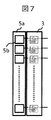
- FIG. 7 is a configuration diagram showing an output circuit area portion in the present embodiment.
- the configuration data area 5 a connected to this area is also set as the overwriting target area of the output circuit area overwriting control unit 8. That is, in FIG. 7, the configuration data area 5a is an area for storing normal circuit information, and overwrites safety data, which is configuration data having logic information for changing the signal level and controlling the order.
- the configuration data area 5a has a block 5b for storing logical information, and is composed of, for example, a lookup table and a flip-flop.
- the output signal can be changed immediately before the output signal of the programmable device 1 is fixed, and the next-stage device component connected to the output signal of the programmable device 1 of the present embodiment can be changed.
- an order control signal for shifting to a safe state can be transmitted. This makes it possible to output a preparation signal once instead of setting it to a fixed value all at once, thus simplifying post-processing measures for abnormal operations that are not normal operations due to the fixation of the output of the previous stage of the next stage device component. It becomes possible.
- FIG. 8 is a configuration diagram of the programmable device according to the present embodiment.
- the same parts as those in FIG. 1 are denoted by the same reference numerals, and description of the parts having the same configuration and operation is omitted.
- a safety data holding unit 13 for holding safety data is provided in the programmable device 1.
- the control operation is the same as in FIG. 1, and safety data is input from the safety data holding unit 13.
- configuration data that is safety data
- it may be stored as logical information in the CRAM. That is, a circuit for fixing the output may be inserted into the CRAM at the stage of defining the circuit structure, and the output may be fixed by enable control or the like. From the above, according to the present embodiment, it is possible to fix the output signal to the signal level for quickly shifting to the safe state immediately before fixing the output signal of the programmable device 1.
- FIG. 9 is a configuration diagram of the programmable device according to the present embodiment.
- the same parts as those in FIG. 1 are denoted by the same reference numerals, and description of the parts having the same configuration and operation is omitted.
- the output circuit area overwrite control unit 8 and the output circuit area address holding unit 9 are separated from the programmable device 1 and configured as separate devices.
- the output circuit area overwrite control unit 8 and the output circuit area address holding unit 9 are stored in the output circuit area overwrite control LSI indicated by 14 and separated from the programmable device 1.
- the control operation is the same as in FIG.
- FIG. 10 is a configuration diagram of the programmable device according to the present embodiment.
- the functional circuit block group 5 for storing the logic circuit information realized by the programmable device 1 has the logic error signals ((1) (2) ( 3)) is received by the error collector 15 and the error signal is output to the output circuit area overwrite controller 8. Then, using this error signal as a trigger, a write process to the area 3 for setting the signal level of the output pin in the CRAM is started. Note that, using both the error detection signal from the CRAM error detection unit 7 and the error signal from the error collection unit 15, a write process to the region 3 for setting the signal level of the output pin in the CRAM is started as a trigger. You may do it.
- the time from the bit inversion of the CRAM to the fixing of the output signal can be increased, and the influence of the post-output that can cause a malfunction can be further reduced.
- FIG. 1 a structure which arrange
- FIG. 10 shows a configuration diagram of the programmable device according to the present embodiment.
- the present embodiment collects the latched output signal temporary latch unit 5c, which is means for temporarily holding the output signal state, and the latched result in the configuration of the sixth embodiment.
- a safety data update unit 13 a that temporarily holds and then updates the safety data 13 is provided.
- FIG. 11 is a configuration diagram of an apparatus substrate on which the programmable device according to the present embodiment is mounted.
- a plurality of programmable devices 1 according to this embodiment are arranged on an apparatus substrate 51, and error signals 54 from the individual programmable devices are collected by an error signal collecting unit 56.
- the error signal collection unit 56 outputs the integrated error signal 55 and outputs it as an external error signal of the programmable device 1 described in the first to seventh embodiments.
- the plurality of programmable devices 1 collectively fix the output signal levels of all the programmable devices, set them to safe state output, and perform safe operation on the next-stage device parts, for example, LSIs 52 and 53. Continue to output the signal level.
- the safety of the apparatus substrate can be improved.
- FIG. 12 shows a configuration diagram of the programmable device according to the present embodiment.
- the same parts as those in FIG. 8 are denoted by the same reference numerals, and description of the parts having the same configuration and operation is omitted.
- an external sensor 50 and a sensor abnormal state determination unit 19 that inputs data from the external sensor and determines an abnormal state by comparing with the normal state are provided.
- the sensor abnormal state determination unit 19 outputs an abnormality detection signal to the output circuit area overwrite control unit 8 and starts a write process to the area 3 where the signal level of the output pin in the CRAM can be set.
- the abnormal state of the sensor connected to the programmable device 1 is detected, and the abnormal state is not propagated to the next device component, thereby improving the safety of the electronic system apparatus to which the sensor is connected. it can.
- FIG. 1 a structure which arrange
- an abnormal state may be detected by OR of the external error shown in FIG. 8 and the data input from the external sensor of the present embodiment, and using that as a trigger, the output signal level may be fixed and set to the safe state output. .
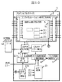
- FIG. 13 shows a configuration diagram of a control device equipped with a programmable device in the present embodiment.
- 57 is a control device
- 58 is a device board group
- 59 is an input / output I / F
- 60a is an input / output device
- 60b is an output device
- 60c is an input device.
- the control device 57 on which the programmable devices of the first to ninth embodiments are mounted is output when a soft error due to environmental radiation or an external error occurs in the programmable device 1 mounted on the device substrate group 58.
- the signal is fixed to an output on the safe side as the device operation, and is output to the input / output device 60a and the output device 60b.
- the present embodiment is a programmable device having a configuration memory and a control device having an input / output I / F.
- the programmable device includes an error detection unit that detects a data reversal failure in the configuration memory, a configuration A control unit that reads and writes the configuration memory, the configuration memory has an output circuit area that stores circuit information for controlling the output signal of the programmable device, and the control unit receives an error from the error detection unit.
- the configuration data is read from the safety data storage unit that stores the configuration data for fixing the output signal level of the programmable device and overwritten in the output circuit area.
- the safety of the control device on which the programmable device is mounted can be improved.
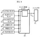
- FIG. 14 is a configuration diagram of an in-vehicle control device in which the programmable devices according to the first to ninth embodiments are mounted according to the present embodiment.
- the engine control unit 68 is configured to input various sensing data from the airflow sensor 61, the cam position sensor 62, the crank position sensor 63, the water temperature sensor 64, the vehicle speed sensor 65, the battery sensor 66, and the like to the programmable device 1. is there.
- the programmable device 1 calculates, generates, and outputs a control signal to the injector 67 based on input data from various sensors.
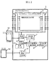
- FIG. 15 is a configuration example of a motor control unit, which is an example of a railway vehicle control device in which the programmable devices according to the first to ninth embodiments are mounted according to the present embodiment.
- an instruction from the on-board controller 79 for controlling the entire railway vehicle is input by the programmable device 1 according to this embodiment.
- the programmable device 1 outputs a drive control signal 75 to the drive circuit 72 that drives the motor 73 in accordance with the instruction from the on-vehicle controller 79 described above.
- the drive circuit receives power from the power supply 71 and outputs tribe signals 77 and 78 to the motor 73.
- the rotation speed and rotation speed of the motor 73 are measured by the encoder 74 and fed back to the programmable device 1.
- the drive control signal 75 outputs incorrect data, causing abnormal acceleration and deceleration.
- the result is fed back from the encoder 74, but the result may also be misinterpreted, leading to a rapid change in the rotational speed.
- the drive control signal 75 by fixing the drive control signal 75 to the state where the motor 73 is stopped, the influence of the feedback of the encoder 74 can be eliminated, and the motor can be stopped safely. Furthermore, by using the programmable device 1 according to the third embodiment, by outputting the drive control signal 75 that gradually decreases the number of rotations of the motor, it is possible to prevent a sudden stop of the railway vehicle and to stop it more safely.
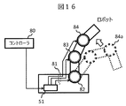
- FIG. 16 is a configuration example of a robot equipped with the programmable device according to the first to ninth embodiments according to the present embodiment.
- 80 is a robot overall control unit
- 81 is a drive unit control signal
- 82, 83, and 84 are robot joint drive units.
- a drive unit control signal 81 is output from the device substrate 51 on which the programmable device 1 according to this embodiment is mounted to the robot joint drive units 82, 83, and 84 that control the movement of the robot. To do.
- the robot joint drive unit 84 in the robot working state is at 84a, if an error occurs in the programmable device 1, the robot joint drive unit is fixed to a signal level that stops immediately. Further, by using the programmable device 1 according to the third embodiment, it is possible to perform an output that gradually moves to the position of the robot joint drive unit 84 that is a safe position.
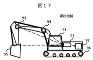
- FIG. 17 is a configuration example of a construction machine in which the first to ninth embodiments are mounted according to the present embodiment.
- 91 is a construction machine main body
- 92 is an engine control unit
- 93 and 94 are arm drive units
- 95 is an excavator
- 96 is a caterpillar, and is constructed from an apparatus substrate 51 on which the programmable device 1 according to this embodiment is mounted.
- Control signals are output to the arm drive units 93 and 94 and the excavator 95 of the machine (indicated by broken arrows in the figure). Further, a movement control signal is also output to the engine control unit 92 that controls the movement operation.
- the drive unit and the engine are fixed to a signal level that immediately stops. Moreover, the drive part can be gradually moved to a safe position by using the programmable device 1 according to the third embodiment.
- the FPGA shifts the output signal to a safe state immediately when an abnormal state that is difficult to assume, such as a failure due to environmental radiation of the configuration memory generated in the programmable device, is generated. It is possible to reduce the risk of dangerous failure of the equipment using this, and contribute to the improvement of the safety of the equipment.
- SIL Safety Integrity level
- IEC International Electrotechnical Commission 61508 regarding functional safety. That is, conventionally, it has been necessary to explain that the set value is on the safe side, but in this embodiment, the output value is fixed to a safety pattern determined by the specifications of the device, so that the explanation is easy. Because. Furthermore, the reliability and safety of the electronic system device can be improved with a simple configuration, and the power consumption and cost can be reduced.
- CRAM Configuration memory
- 5 ... functional circuit block group 5a ... configuration data area
- 5b block for storing logic information
- 5c output signal temporary latch unit
- 6 ... CRAM R / W control unit 7 ... CRAM error detection unit
- 8 ... Output circuit area overwrite control unit 9 ... Output circuit area address holding unit, 10 ... external storage unit, 11 ... configuration data, 12 ... safety data, 13 ... Safety data storage unit, 13a ... Safety data update unit, 14 ...
- error aggregation signal 56 ... error collection unit, 57 ... Control device, 58 ... Device board group, 68 ... Engine control unit, 72 ... Drive circuit, 73 ... Motor body, 75 ... Drive control signal, 77, 78 ... Drive signal, 80 ... Overall robot control unit, 81 ... Drive unit control signal, 82, 83, 84 ... Robot joint drive unit, 91 ... Construction machine body, 92 ... Engine control unit
Landscapes
- Physics & Mathematics (AREA)
- Engineering & Computer Science (AREA)
- Computer Hardware Design (AREA)
- Computing Systems (AREA)
- General Engineering & Computer Science (AREA)
- Mathematical Physics (AREA)
- Logic Circuits (AREA)
- Programmable Controllers (AREA)
Abstract
Le problème selon la présente invention est que, lorsqu'un état anormal difficile à prévoir se produit, tel qu'une défaillance due à un rayonnement environnemental qui se produit dans une mémoire de configuration d'un dispositif programmable, ce qui provoque une anomalie de signal de sortie, une opération dangereuse peut se produire dans l'appareil dans lequel est monté le dispositif. Pour résoudre le problème mentionné ci-dessus, la présente invention concerne un dispositif programmable ayant une mémoire de configuration, le dispositif programmable comprenant une partie de détection d'erreur qui détecte un défaut d'inversion de données dans la mémoire de configuration, et une partie de commande qui commande la lecture et l'écriture de la mémoire de configuration, la mémoire de configuration comportant une région de circuit de sortie stockant des informations de circuit pour commander le signal de sortie du dispositif programmable, et la partie de commande étant déclenchée par un signal de détection d'erreur provenant de la partie de détection d'erreur de sorte à lire des données de configuration pour fixer le niveau de signal de sortie du dispositif programmable à partir d'une partie de stockage de données sécurisées stockant les données de configuration et à écraser les données de configuration à la région de circuit de sortie.
Priority Applications (2)
| Application Number | Priority Date | Filing Date | Title |
|---|---|---|---|
| PCT/JP2015/050283 WO2016110968A1 (fr) | 2015-01-07 | 2015-01-07 | Dispositif programmable, appareil de commande utilisant ce dernier et procédé de contre-mesure en cas de défaillance |
| JP2016568214A JP6263649B2 (ja) | 2015-01-07 | 2015-01-07 | プログラマブルデバイス及びそれを用いた制御装置、及びその障害対策方法 |
Applications Claiming Priority (1)
| Application Number | Priority Date | Filing Date | Title |
|---|---|---|---|
| PCT/JP2015/050283 WO2016110968A1 (fr) | 2015-01-07 | 2015-01-07 | Dispositif programmable, appareil de commande utilisant ce dernier et procédé de contre-mesure en cas de défaillance |
Publications (1)
| Publication Number | Publication Date |
|---|---|
| WO2016110968A1 true WO2016110968A1 (fr) | 2016-07-14 |
Family
ID=56355690
Family Applications (1)
| Application Number | Title | Priority Date | Filing Date |
|---|---|---|---|
| PCT/JP2015/050283 Ceased WO2016110968A1 (fr) | 2015-01-07 | 2015-01-07 | Dispositif programmable, appareil de commande utilisant ce dernier et procédé de contre-mesure en cas de défaillance |
Country Status (2)
| Country | Link |
|---|---|
| JP (1) | JP6263649B2 (fr) |
| WO (1) | WO2016110968A1 (fr) |
Cited By (2)
| Publication number | Priority date | Publication date | Assignee | Title |
|---|---|---|---|---|
| CN110262440A (zh) * | 2019-07-26 | 2019-09-20 | 中车青岛四方车辆研究所有限公司 | 轨道车辆牵引系统用数据监控采集系统及方法 |
| WO2021152887A1 (fr) * | 2020-01-27 | 2021-08-05 | 株式会社日立製作所 | Dispositif programmable et contrôleur de commande faisant appel à ce dernier |
Citations (4)
| Publication number | Priority date | Publication date | Assignee | Title |
|---|---|---|---|---|
| JP2000357962A (ja) * | 1998-09-09 | 2000-12-26 | Hitachi Ltd | 半導体集積回路装置 |
| JP2007058419A (ja) * | 2005-08-23 | 2007-03-08 | Hitachi Ltd | Pld上のメモリ内の情報に従って構築される論理回路を備えたストレージシステム |
| JP2008015965A (ja) * | 2006-07-10 | 2008-01-24 | Fuji Xerox Co Ltd | 情報処理装置、情報処理装置の動作方法およびプログラム |
| JP2013187699A (ja) * | 2012-03-07 | 2013-09-19 | Fujitsu Telecom Networks Ltd | Fpga構成処理制御回路 |
Family Cites Families (1)
| Publication number | Priority date | Publication date | Assignee | Title |
|---|---|---|---|---|
| JPS58127432A (ja) * | 1982-01-25 | 1983-07-29 | Nippon Telegr & Teleph Corp <Ntt> | 論理アレイ装置 |
-
2015
- 2015-01-07 WO PCT/JP2015/050283 patent/WO2016110968A1/fr not_active Ceased
- 2015-01-07 JP JP2016568214A patent/JP6263649B2/ja active Active
Patent Citations (4)
| Publication number | Priority date | Publication date | Assignee | Title |
|---|---|---|---|---|
| JP2000357962A (ja) * | 1998-09-09 | 2000-12-26 | Hitachi Ltd | 半導体集積回路装置 |
| JP2007058419A (ja) * | 2005-08-23 | 2007-03-08 | Hitachi Ltd | Pld上のメモリ内の情報に従って構築される論理回路を備えたストレージシステム |
| JP2008015965A (ja) * | 2006-07-10 | 2008-01-24 | Fuji Xerox Co Ltd | 情報処理装置、情報処理装置の動作方法およびプログラム |
| JP2013187699A (ja) * | 2012-03-07 | 2013-09-19 | Fujitsu Telecom Networks Ltd | Fpga構成処理制御回路 |
Cited By (6)
| Publication number | Priority date | Publication date | Assignee | Title |
|---|---|---|---|---|
| CN110262440A (zh) * | 2019-07-26 | 2019-09-20 | 中车青岛四方车辆研究所有限公司 | 轨道车辆牵引系统用数据监控采集系统及方法 |
| CN110262440B (zh) * | 2019-07-26 | 2021-05-04 | 中车青岛四方车辆研究所有限公司 | 轨道车辆牵引系统用数据监控采集系统及方法 |
| WO2021152887A1 (fr) * | 2020-01-27 | 2021-08-05 | 株式会社日立製作所 | Dispositif programmable et contrôleur de commande faisant appel à ce dernier |
| JP2021117720A (ja) * | 2020-01-27 | 2021-08-10 | 株式会社日立製作所 | プログラマブルデバイス及びこれを用いた制御コントローラ |
| JP7157773B2 (ja) | 2020-01-27 | 2022-10-20 | 株式会社日立製作所 | プログラマブルデバイス及びこれを用いた制御コントローラ |
| US11822425B2 (en) | 2020-01-27 | 2023-11-21 | Hitachi, Ltd. | Programmable device, and controller using the same |
Also Published As
| Publication number | Publication date |
|---|---|
| JP6263649B2 (ja) | 2018-01-17 |
| JPWO2016110968A1 (ja) | 2017-04-27 |
Similar Documents
| Publication | Publication Date | Title |
|---|---|---|
| JP5699057B2 (ja) | プログラマブルデバイス、プログラマブルデバイスのリコンフィグ方法および電子デバイス | |
| CN111275606B (zh) | 工作量重复冗余 | |
| CN103984630B (zh) | 一种基于at697处理器的单粒子翻转故障处理方法 | |
| CN103679011B (zh) | 半导体集成电路 | |
| JP5014899B2 (ja) | 再構成可能デバイス | |
| US12086692B2 (en) | Devices and method for monitoring a quantum computer in operation | |
| CN102968363B (zh) | 用于保护和无损地检查与安全相关的寄存器的装置和方法 | |
| CN106484581A (zh) | 空间辐射环境下可编程soc器件单粒子翻转检测系统及方法 | |
| US8527714B2 (en) | Secure avionics equipment and associated method of making secure | |
| JP6290934B2 (ja) | プログラマブルデバイス、エラー保持システム、及び電子システム装置 | |
| CN101916306A (zh) | 一种用于fpga芯片敏感区域定位的系统及其方法 | |
| JP6263649B2 (ja) | プログラマブルデバイス及びそれを用いた制御装置、及びその障害対策方法 | |
| CN116382951A (zh) | 可编程信号聚合器 | |
| JP2014209312A (ja) | 集積回路 | |
| CN100368997C (zh) | 一种静态数据存储的纠错编码装置 | |
| JP6332134B2 (ja) | メモリ診断回路 | |
| CN201828914U (zh) | 一种用于fpga芯片敏感区域定位的系统 | |
| JP5838103B2 (ja) | 電子装置、ソフトエラー耐性評価システム及び評価方法 | |
| WO2014115289A1 (fr) | Dispositif programmable et dispositif de système électronique | |
| US9772897B1 (en) | Methods and systems for improving safety of processor system | |
| Bridgford et al. | Correcting single-event upsets in virtex-ii platform fpga configuration memory | |
| US10749547B2 (en) | Error detector and/or corrector checker method and apparatus | |
| KR102899319B1 (ko) | 프로세스 검사 장치 및 방법과, 전자 제어 장치 | |
| US12332733B2 (en) | Determining an error handling mode | |
| US20110022903A1 (en) | Device enabling the use of a programmable component in a natural radiative environment |
Legal Events
| Date | Code | Title | Description |
|---|---|---|---|
| 121 | Ep: the epo has been informed by wipo that ep was designated in this application |
Ref document number: 15876846 Country of ref document: EP Kind code of ref document: A1 |
|
| ENP | Entry into the national phase |
Ref document number: 2016568214 Country of ref document: JP Kind code of ref document: A |
|
| NENP | Non-entry into the national phase |
Ref country code: DE |
|
| 122 | Ep: pct application non-entry in european phase |
Ref document number: 15876846 Country of ref document: EP Kind code of ref document: A1 |