WO2016114336A1 - 光学素子及び光学素子の製造方法 - Google Patents
光学素子及び光学素子の製造方法 Download PDFInfo
- Publication number
- WO2016114336A1 WO2016114336A1 PCT/JP2016/050918 JP2016050918W WO2016114336A1 WO 2016114336 A1 WO2016114336 A1 WO 2016114336A1 JP 2016050918 W JP2016050918 W JP 2016050918W WO 2016114336 A1 WO2016114336 A1 WO 2016114336A1
- Authority
- WO
- WIPO (PCT)
- Prior art keywords
- optical element
- resin
- optical
- light source
- glass filler
- Prior art date
- Legal status (The legal status is an assumption and is not a legal conclusion. Google has not performed a legal analysis and makes no representation as to the accuracy of the status listed.)
- Ceased
Links
Images



Classifications
-
- G—PHYSICS
- G02—OPTICS
- G02B—OPTICAL ELEMENTS, SYSTEMS OR APPARATUS
- G02B3/00—Simple or compound lenses
-
- G—PHYSICS
- G02—OPTICS
- G02B—OPTICAL ELEMENTS, SYSTEMS OR APPARATUS
- G02B6/00—Light guides; Structural details of arrangements comprising light guides and other optical elements, e.g. couplings
- G02B6/02—Optical fibres with cladding with or without a coating
- G02B6/02295—Microstructured optical fibre
-
- B—PERFORMING OPERATIONS; TRANSPORTING
- B29—WORKING OF PLASTICS; WORKING OF SUBSTANCES IN A PLASTIC STATE IN GENERAL
- B29C—SHAPING OR JOINING OF PLASTICS; SHAPING OF MATERIAL IN A PLASTIC STATE, NOT OTHERWISE PROVIDED FOR; AFTER-TREATMENT OF THE SHAPED PRODUCTS, e.g. REPAIRING
- B29C45/00—Injection moulding, i.e. forcing the required volume of moulding material through a nozzle into a closed mould; Apparatus therefor
- B29C45/0001—Injection moulding, i.e. forcing the required volume of moulding material through a nozzle into a closed mould; Apparatus therefor characterised by the choice of material
-
- B—PERFORMING OPERATIONS; TRANSPORTING
- B29—WORKING OF PLASTICS; WORKING OF SUBSTANCES IN A PLASTIC STATE IN GENERAL
- B29C—SHAPING OR JOINING OF PLASTICS; SHAPING OF MATERIAL IN A PLASTIC STATE, NOT OTHERWISE PROVIDED FOR; AFTER-TREATMENT OF THE SHAPED PRODUCTS, e.g. REPAIRING
- B29C45/00—Injection moulding, i.e. forcing the required volume of moulding material through a nozzle into a closed mould; Apparatus therefor
- B29C45/0013—Injection moulding, i.e. forcing the required volume of moulding material through a nozzle into a closed mould; Apparatus therefor using fillers dispersed in the moulding material, e.g. metal particles
-
- B—PERFORMING OPERATIONS; TRANSPORTING
- B29—WORKING OF PLASTICS; WORKING OF SUBSTANCES IN A PLASTIC STATE IN GENERAL
- B29C—SHAPING OR JOINING OF PLASTICS; SHAPING OF MATERIAL IN A PLASTIC STATE, NOT OTHERWISE PROVIDED FOR; AFTER-TREATMENT OF THE SHAPED PRODUCTS, e.g. REPAIRING
- B29C45/00—Injection moulding, i.e. forcing the required volume of moulding material through a nozzle into a closed mould; Apparatus therefor
- B29C45/17—Component parts, details or accessories; Auxiliary operations
- B29C45/72—Heating or cooling
- B29C45/73—Heating or cooling of the mould
-
- G—PHYSICS
- G02—OPTICS
- G02B—OPTICAL ELEMENTS, SYSTEMS OR APPARATUS
- G02B1/00—Optical elements characterised by the material of which they are made; Optical coatings for optical elements
- G02B1/04—Optical elements characterised by the material of which they are made; Optical coatings for optical elements made of organic materials, e.g. plastics
-
- G—PHYSICS
- G02—OPTICS
- G02B—OPTICAL ELEMENTS, SYSTEMS OR APPARATUS
- G02B6/00—Light guides; Structural details of arrangements comprising light guides and other optical elements, e.g. couplings
- G02B6/24—Coupling light guides
- G02B6/42—Coupling light guides with opto-electronic elements
- G02B6/4201—Packages, e.g. shape, construction, internal or external details
- G02B6/4204—Packages, e.g. shape, construction, internal or external details the coupling comprising intermediate optical elements, e.g. lenses, holograms
- G02B6/4214—Packages, e.g. shape, construction, internal or external details the coupling comprising intermediate optical elements, e.g. lenses, holograms the intermediate optical element having redirecting reflective means, e.g. mirrors, prisms for deflecting the radiation from horizontal to down- or upward direction toward a device
-
- B—PERFORMING OPERATIONS; TRANSPORTING
- B29—WORKING OF PLASTICS; WORKING OF SUBSTANCES IN A PLASTIC STATE IN GENERAL
- B29C—SHAPING OR JOINING OF PLASTICS; SHAPING OF MATERIAL IN A PLASTIC STATE, NOT OTHERWISE PROVIDED FOR; AFTER-TREATMENT OF THE SHAPED PRODUCTS, e.g. REPAIRING
- B29C45/00—Injection moulding, i.e. forcing the required volume of moulding material through a nozzle into a closed mould; Apparatus therefor
- B29C45/17—Component parts, details or accessories; Auxiliary operations
- B29C45/72—Heating or cooling
- B29C45/73—Heating or cooling of the mould
- B29C2045/7356—Heating or cooling of the mould the temperature of the mould being near or higher than the melting temperature or glass transition temperature of the moulding material
-
- B—PERFORMING OPERATIONS; TRANSPORTING
- B29—WORKING OF PLASTICS; WORKING OF SUBSTANCES IN A PLASTIC STATE IN GENERAL
- B29K—INDEXING SCHEME ASSOCIATED WITH SUBCLASSES B29B, B29C OR B29D, RELATING TO MOULDING MATERIALS OR TO MATERIALS FOR MOULDS, REINFORCEMENTS, FILLERS OR PREFORMED PARTS, e.g. INSERTS
- B29K2995/00—Properties of moulding materials, reinforcements, fillers, preformed parts or moulds
- B29K2995/0018—Properties of moulding materials, reinforcements, fillers, preformed parts or moulds having particular optical properties, e.g. fluorescent or phosphorescent
- B29K2995/0026—Transparent
-
- G—PHYSICS
- G02—OPTICS
- G02B—OPTICAL ELEMENTS, SYSTEMS OR APPARATUS
- G02B7/00—Mountings, adjusting means, or light-tight connections, for optical elements
- G02B7/02—Mountings, adjusting means, or light-tight connections, for optical elements for lenses
- G02B7/028—Mountings, adjusting means, or light-tight connections, for optical elements for lenses with means for compensating for changes in temperature or for controlling the temperature; thermal stabilisation
Definitions
- the present invention relates to an optical element suitably used for, for example, optical communication and a method for manufacturing the optical element.
- an optical transmission module including a light emitting element that converts an electrical signal into an optical signal and transmits the optical signal
- an optical reception module including a light receiving element that receives the optical signal and converts it into an electrical signal.
- an optical transceiver module having both functions is used as a main optical component.
- optical coupling device is generally used for optical coupling between the optical fiber and the optical module.
- optical fibers are basically flexible, so that they can be bent and slack to some extent.
- the minimum bend diameter allowed to ensure light transmission efficiency is specified. Has been. Therefore, when bending less than the minimum diameter is required due to installation space restrictions, etc., the optical fiber is cut and the optical coupling is performed by bending the optical path of the light beam transmitted between the cut optical fibers.
- the use of the coupling device may lead to more efficient storage as a whole and increase the light transmission efficiency.
- the merit of using such an optical coupling device is not limited to optical fibers, but can also occur in optical coupling between a light emitting element and an optical fiber or between an optical fiber and a light receiving element.
- the light emitting element, the light source, the light receiving element, and the like are collectively referred to as an optical element.
- an optical connector having a structure in which an optical path is bent may be used in an optical coupling device.
- a PT optical connector (standardized by JPCA-PE03-01-06S) that changes the optical axis by 90 ° inside the connector has been put into practical use.
- the PT optical connector is a board-mounted optical connector that optically couples a multi-core optical fiber such as a multi-core optical fiber tape core wire and an optical element on a flexible wiring board.
- the single mode fiber is an ultrafine fiber having a mode field diameter of 9.2 ⁇ m, and has an advantage that attenuation can be suppressed as much as possible by setting the propagation of the optical signal to one mode. Therefore, unlike a transmission method that uses many modes such as multimode fiber, the signal arrival time is single, so there is no mode loss and it is suitable for long-distance and high-speed transmission. Opportunities for fiber use have increased.
- An optical connector used for such an application generally has a plurality of lens surfaces for propagating light to individual optical fibers and optical elements, but when such an optical connector is formed from a resin, For example, due to thermal expansion due to changes in environmental temperature, there is a possibility that the optical fiber core-to-core distance and the distance between the lens surfaces may be shifted, thereby making it impossible to perform optical coupling between some optical fibers and optical elements. . On the other hand, in order to suppress optical loss at the time of information transmission, the optical connector needs to secure a certain degree of transparency (transmittance).
- Patent Documents 1 and 2 there is an attempt to mold an optical element with a material close to the characteristics of glass by mixing a glass filler into a resin.
- Patent Documents 1 and 2 a technique for increasing the mechanical strength by mixing a glass filler into a resin and further ensuring the transparency of the resin by bringing the refractive index closer to glass is disclosed.
- the materials disclosed in the above-described prior art are required to have both physical properties of transparency and strength, such as a cover for a display unit of an electric device or an electronic device, or a substitute for a plate glass used in an automobile or a building material.
- the present invention has been made in view of the above-described problems, and is used in an application that transmits a single light source wavelength, can ensure high light use efficiency, and is stable in an external environment and manufacture of an optical element. It aims to provide a method.
- an optical element reflecting one aspect of the present invention is an optical element that transmits a light beam emitted from a light source having a single light source wavelength.
- the optical element is formed of a material in which a resin and a glass filler are mixed, and at least in the vicinity of the light source wavelength, a difference in refractive index change amount (dn / dT) with respect to a temperature change of the resin and the glass filler is 10.5 ⁇ 10 ⁇ 5 or less.
- the transmittance changes with respect to the wavelength, and the wavelength with the highest transmittance (referred to as the peak wavelength) occurs. It was assumed to be unchanged regardless of the amount of contamination.
- the peak wavelength the wavelength with the highest transmittance
- the light source wavelength is determined in advance, it can be said that it is not necessary to ensure the transmittance in the entire wavelength band. Therefore, in the design of an optical element for a single light source wavelength, for example, in order to adjust the linear expansion coefficient, a policy of using a resin material appropriately mixed with a glass filler has been decided.
- the term “refractive index” refers to the refractive index at room temperature (25 ° C.), unless otherwise specified.
- the expression “mixed” is used because it is sufficient if the resin material and the glass filler are mixed.
- the expression “mixed” is used in this description. Sometimes used to explain.
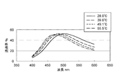
- the vertical axis represents the transmittance
- the horizontal axis represents the wavelength
- the wavelength of each of the test pieces having a thickness of 3 mm made of a resin mixed with 30 wt% glass filler is changed while the ambient temperature is changed.
- FIG. 2 is an enlarged schematic view of a resin mixed with a glass filler.
- the resin PL a large number of rod-shaped body pieces of glass filler GF are arranged so as to overlap each other.
- the resin mixed with the glass filler is first heated to about 300 ° C., injected into a mold heated to about 120 ° C., and then solidified. Leave at room temperature around °C.
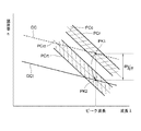
- FIG. 3 is a diagram showing the refractive index on the vertical axis and the wavelength on the horizontal axis.
- the inventors of the present invention are that the original refractive index / wavelength characteristics of the resin PL and the glass filler GF are both limited to a narrow wavelength range (for example, light source wavelength ⁇ 100 nm), and the wavelength ⁇ of the transmitted light is high. It is assumed that the linear characteristic is such that the refractive index n decreases as the time increases. However, in reality, it is presumed that the refractive index of the resin PL changes locally by mixing the glass filler GF, so that the refractive index / wavelength characteristics of the resin PL are predetermined as shown by hatching in FIG.
- the peak wavelength at normal temperature is the position of the point PK1 where the refractive index characteristic PCc having the most distributed density amount in the band-like region PCr and the refractive index / wavelength characteristic line GC of the glass filler GF indicated by the dotted line intersect. It is assumed that
- the glass filler GF is scattered while the refractive index distribution inside the molded product is relatively large, the wavelengths transmitted through the respective glass fillers are different. Inferred to be a factor.
- the refractive index / wavelength characteristic of the resin PL becomes a band-shaped region PCrt shifted to the short wavelength side while being varied within a predetermined range, as shown in FIG.
- the density of the glass filler GF also decreases slightly, so that the refractive index also decreases accordingly and shifts as shown by the solid line in FIG.
- the peak wavelength at the time of temperature rise is the point PK2 where the refractive index characteristic PCct having the most distributed density amount in the band-like region PCrt in the resin PL and the refractive index / wavelength characteristic line GCt of the glass filler GF intersect. Inferred to be in position.
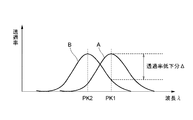
- FIG. 4 is a diagram schematically showing the characteristics of a resin mixed with glass filler at normal temperature (A) and temperature rise (B), where the vertical axis represents transmittance and the horizontal axis represents wavelength. .
- a transmittance distribution occurs, but here a Gaussian distribution centered on the peak wavelength is used.
- the peak wavelength PK1 shifts to the lower peak wavelength PK2, but assuming that the single light source wavelength is PK1, the temperature Since the resin material follows the characteristic (B) when it rises, it can be seen that the transmittance decreases by ⁇ .
- the peak wavelength at 28 ° C. is 503 nm and the transmittance is 52.1%.
- the peak wavelength was 490 nm
- the transmittance was reduced to 51.7%
- the peak wavelength was 480 nm
- the transmittance at a wavelength of 503 nm was reduced to 51.4%
- the peak wavelength was 476 nm and the transmittance was reduced to 51.2%.
- the present inventors have found that the above-described problems can be solved by devising the amount of change in the refractive index with respect to the temperature change of the resin and the mixed glass filler. More specifically, in FIG. 3, if the peak wavelength PK1 at the normal temperature overlaps with the peak wavelength PK2 at the time of the temperature rise, a decrease in transmittance can be suppressed as much as possible. In other words, in FIG. 5 in which the vertical axis represents the refractive index and the horizontal axis represents the wavelength, the refractive index characteristic PCc having the most distributed density amount in the band-shaped region PCr of the resin PL at room temperature.
- a refractive index characteristic PCct having a density amount most distributed in the band-like region PCrt of the resin PL when the temperature rises with respect to a point PK1 where the refractive index / wavelength characteristic line GC of the glass filler GF intersects, If the point PK2 where the refractive index / wavelength characteristic line GCt of the glass filler GF intersects is overlapped on the horizontal axis, the shift of the peak wavelength can be suppressed regardless of the temperature change. However, even if the peak wavelengths PK1 and PK2 do not completely match, it is effective if the difference is small.
- the entire wavelength range of the visible light region is required, so the refractive index of the glass filler and the resin should be the same as much as possible in the entire wavelength range. It is conceivable to select such a material. However, since this embodiment uses a single light source, the refractive index of the glass filler and the resin should not be the same as much as possible in the entire wavelength range as in optical element applications for the purpose of transmitting subject light and displaying color images.
- the amount of change in refractive index (dn / dT) with respect to temperature change is 10.5 ⁇ 10 ⁇ 5 or less, it can be used for the optical element of this embodiment.
- near the light source wavelength means a range of ⁇ 100 nm with respect to the light source wavelength.
- a primary or secondary approximate curve using a refractive index near the light source wavelength may be used.
- another optical element reflecting one aspect of the present invention is an optical element that transmits a light beam emitted from a light source having a single light source wavelength.
- the optical element is formed of a material in which a resin and a glass filler are mixed, and a difference in linear expansion coefficient between the resin and the glass filler is 6.0 ⁇ 10 ⁇ at least in a use temperature range of the optical element. 5 or less.
- the glass filler and the resin so that the difference in linear expansion coefficient between the resin and the glass filler is 6.0 ⁇ 10 ⁇ 5 or less at least in the operating temperature range of the optical element.
- the shift amount of the peak wavelength at the time of temperature change can be suppressed with respect to the peak wavelength at the normal temperature in an optical element molded using such a material. Reduction in rate can be suppressed.
- the difference in linear expansion coefficient between the resin and the glass filler is 6.0 ⁇ 10 ⁇ 5 or less, the glass filler expands or contracts in the same manner as the resin when the temperature changes (increases or decreases).
- the “operating temperature range” refers to a range of ⁇ 20 ° C. to 85 ° C.
- an optical element manufacturing method transmits a light beam emitted from a light source having a single light source wavelength, and includes a resin and a glass filler.
- a method of manufacturing an optical element formed from a material mixed with A mixing step of mixing a resin and a glass filler in which a difference in refractive index change (dn / dT) with respect to a temperature change between the resin and the glass filler is 10.5 ⁇ 10 ⁇ 5 or less at least in the vicinity of the light source wavelength.
- another method of manufacturing an optical element reflecting one aspect of the present invention transmits a light beam emitted from a light source having a single light source wavelength, and is made of resin and glass.
- a method of manufacturing an optical element formed from a material mixed with a filler A mixing step of mixing a resin and a glass filler in which a difference in linear expansion coefficient between the resin and the glass filler is 6.0 ⁇ 10 ⁇ 5 or less, at least in a use temperature range of the optical element; Injecting the mixed material into a cavity formed in a mold; Cooling the mixed material in the mold to mold an optical element; Removing the molded optical element; It is characterized by having.
- an optical element that is used for transmitting a single light source wavelength, can secure high light use efficiency, and is stable with respect to the external environment, and a method for manufacturing the optical element.
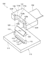
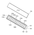
- FIG. 3 is a perspective view of an optical path changing element 120 used in the optical coupling device 100.
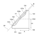
- FIG. 3 is an enlarged sectional view of an optical path changing element 120.
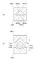
- FIG. It is a figure which shows the process of shape
- the term “single light source wavelength” means that the light source wavelength used for a specific purpose is single.
- the same optical element is used for upstream communication and downstream communication. Even when used, the light source wavelength may be different. In such a case, this means that the light source wavelength during uplink communication is single and the light source wavelength during downlink communication is single.
- glass filler general-purpose E glass, C glass, A glass, S glass, D glass, NE glass, T glass, quartz glass and the like may be used.
- glass fiber glass fiber
- glass powder glass powder
- glass flake milled fiber
- glass bead glass bead, or the like
- glass fibers will be described on behalf of glass fillers.
- the glass fiber can be obtained by using a conventionally known method for spinning long glass fibers.
- the glass raw material is continuously vitrified in a melting furnace, led to fore-haas, and a direct melt (DM) method in which a bushing is attached to the bottom of the fore-heart and spun, or the melted glass is processed into marble, cullet, or rod shape
- DM direct melt
- the glass can be made into fiber using various methods such as a remelting method in which it is remelted and spun.
- the diameter of the glass fiber is not particularly limited, but a glass fiber having a diameter of 5 to 50 ⁇ m is preferably used. If it is thinner than ⁇ 5 ⁇ m, the contact area between the glass fiber and the resin is increased, causing irregular reflection, and the transparency of the molded product may be lowered. If it is thicker than ⁇ 50 ⁇ m, the filling pressure at the time of injection molding becomes high, which may lead to insufficient transfer to the mold. More preferably, it is ⁇ 10 to ⁇ 45 ⁇ m.
- the glass filler it is important for the glass filler that particles having a size larger than the light source wavelength are 90% or more (preferably 95% or more) of the whole.
- a resin material mixed with particles having a diameter of 30 nm or less, for example.
- this resin material there is a problem that particles are likely to aggregate, and the surface area of the particles increases.
- the problem is that the resin material tends to become hard and molding becomes difficult, and further, the surface area of the particles increases to increase the hydrophilicity, and the water absorption of the molded optical element increases to change the optical characteristics. there were.
- this problem can be solved by making the glass filler particles larger than the light source wavelength.
- the “optical element” for example, a lens, a prism, a diffraction grating element (diffraction lens, diffraction prism, diffraction plate), an optical filter (spatial low-pass filter, wavelength band-pass filter, wavelength low-pass filter, wavelength high-pass filter, etc.), Examples include a polarizing filter (analyzer, optical rotator, polarization separating prism, etc.) and a phase filter (phase plate, hologram, etc.), but are not limited thereto.
- FIG. 6 is a perspective view showing the optical coupling device 100 having the optical path changing element as the optical element according to the present embodiment in an exploded state.
- FIG. 7 is a cross-sectional view of the optical coupling device 100 along the optical axis.
- FIG. 8 is a perspective view of the optical path changing element 120 used in the optical coupling device 100.
- FIG. 9 is an enlarged cross-sectional view of the optical path changing element 120.
- the following configuration is a schematic diagram, and some shapes, dimensions, and the like are different from actual ones.
- the optical coupling device 100 includes an optical module 110, an optical path changing element 120, and an optical connector 130.
- the optical module 110 has a function of transmitting light, and can be installed on a substrate that is stacked and inserted on the back surface of a large-capacity server or the like.
- the substrate itself may be the optical module 110.
- the optical module 110 includes a plurality of VCSEL type semiconductor lasers 112 which are light emitting elements arranged in a row on a base plate 111 having a rectangular shape and a flat upper surface.
- the light source wavelength of the semiconductor laser 112 is any one of 850 nm, 1310 nm, and 1550 nm.
- the NA of the optical module 110 is 0.1 to 0.6.
- the optical connector 130 includes a main body 131 formed of a resin, and is connected to the optical fiber 132 and has a function of holding it.
- optical fiber 132 for example, an all-quartz multimode optical fiber or a single mode optical fiber can be used.
- a single-core optical fiber may be used, but here, a multi-core optical fiber tape (ribbon) having a plurality of optical fibers is used.
- the main body 131 is formed in a thick rectangular plate shape, and one side is cut out in a rectangular shape when viewed from above in FIG. 6 to form a recess 131a.
- an insertion hole 131 b for inserting the optical fiber 132 is formed on the opposite side of the main body 131 from the recess 131 a.
- the insertion hole 131b has a wide rectangular cross section so that the protection part 132a as a coating of the optical fiber 132 can be accommodated.
- a plurality of thin through holes 131c are formed from the bottom surface of the insertion hole 131b toward the recess 131a. The tip of the fiber strand 132b from which the coating of the optical fiber 132 has been removed is inserted into the through hole 131c.
- the bottom surface 131d of the recess 131a where the through hole 131c is exposed is orthogonal to the lower surface 131e of the main body 131.
- a pair of circular openings 131f having the same diameter as the pin 113 are formed on both sides of the recess 131a so as to sandwich the recess 131a.
- the optical path changing element 120 is integrally formed of a resin mixed with a predetermined amount of glass fiber as will be described later.
- the optical path changing element 120 has an elongated triangular prism shape, and has a first surface 121, a second surface 122, and a third surface 123.
- the first surface 121 and the third surface 123 are orthogonal to each other.
- size of the optical axis direction (OA1, OA2 direction) of the optical path change element 120 is 10 mm or less. Further, from the viewpoint that the optical fiber can be made smaller than the minimum diameter when the optical fiber is bent, the size is more preferably 5 mm or less.
- the length of the light beam path passing through the optical element is preferably about 1 mm.
- the length of the light path is smaller than 1 mm, it is possible to use a material having a low transmittance, and conversely, when the length of the light path is larger than 1 mm, a material having a high transmittance is used. By using it, it is possible to ensure a sufficient transmittance as an optical path polarizing element.
- the first surface 121 is a flat surface, and has a function of entering a light beam emitted from the semiconductor laser 112 of the optical module 110.
- the second surface 122 includes a plurality of reflective surfaces 122a arranged in a line, a planar connecting surface 122b formed around the reflecting surface 122a, and an outer periphery of the second surface 122 so as to surround the connecting surface 122b. And a protruding portion 122c having a rectangular frame shape. It is preferable that an inclined surface 122d is formed between the connecting surface 122b and the protruding portion 122c.
- the third surface 123 is a flat surface and has a function of transmitting the light beam reflected from the reflecting surface 122a.
- Each of the reflecting surfaces 122a has the same shape protruding from the connecting surface 122b.
- the reflecting surface 122a has an elliptical shape when viewed from the front, and bends the optical axis by 90 ° when a conical divergent light beam is incident. It has an anamorphic free-form surface that can reflect a conical convergent light beam.
- a toroidal surface an anamorphic surface in a broad sense having an elliptical shape in one direction is formed. Thereby, the aberration can be almost eliminated.
- the arrangement interval of the reflecting surfaces 122a is equal to the arrangement interval of the semiconductor lasers 112 of the optical module 110 and the arrangement interval of the fiber strands 132b inserted into the through holes 131c.
- the arrangement direction of the reflection surfaces 122a is a direction orthogonal to a surface including two optical axes of one reflection surface 122a.
- the angle (acute angle) formed between the tangential plane at the outer peripheral edge of the reflecting surface 122a and the optical axis is usually 75 degrees or less.
- the distance between the protrusion 122c and the reflecting surface 122a is preferably 0.05 mm or more from the viewpoint of not affecting the coupling efficiency.
- the height from the connecting surface 122b of the protruding portion 122c is uniform over the entire circumference, and is larger than the protruding amount of the reflecting surface 122a. Therefore, as shown in FIG. 9, when the virtual plane VP that contacts the entire circumference (here, the plane portion) of the protrusion 122c is defined, the virtual plane VP does not contact the reflecting surface 122a.
- the virtual plane VP is parallel to a tangential plane at an arbitrary point on the reflecting surface 122a (in this example, the point PT on the optical axis is at least a point inside the outer peripheral edge of the reflecting surface 122a). ing.
- the optical axes OA1 and OA2 are orthogonal on the reflective surface 122a.
- the distance along the optical axis OA1 from the first surface 121 to the reflective surface 122a is A, and the point on the optical axis OA1 of the reflective surface 122a
- the distance A is usually 0.0625 mm or more and 2.9 mm or less.
- the optical path changing element 120 has a parallel plate-like cover member 125 bonded to the entire periphery of the protruding portion 122c so as to overlap the virtual plane VP. It is preferable that the cover member 125 is a light-shielding member because deterioration of the optical path changing element 120 can be suppressed and light from the outside can be prevented from entering the lens.
- the cover member 125 is provided, a gap is formed between the reflective surface 122a and the cover member 125 damages the reflective surface 122a, or a reflective film is formed on the reflective surface 122a. There is no risk of injury.
- the cover member 125 can be provided so as to overlap the virtual plane VP, it is possible to contribute to miniaturization in the stacking direction even when the substrate provided with the optical coupling device 100 is stacked. Furthermore, by sealing the reflective surface 122a in a sealed space with the cover member 125, the reflective surface 122a can be protected from adverse effects of the external environment, such as adhesion of foreign matter. Further, the gap between the reflecting surface 122a and the virtual plane VP may be sealed with a resin to prevent the attachment of foreign matter and condensation. Although sealing with the cover member 125 or resin is not necessarily performed, it is preferable to perform sealing with the cover member 125 or resin for the reasons described above. As shown in FIG. 9, it is preferable that the cover member 125 has a shape that does not protrude outward from the optical path changing element 120 when attached to the optical path changing element 120 because the optical coupling device 100 can be downsized.
- FIG. 10 is a diagram illustrating a molding process of the optical path changing element using a resin.
- the first mold MD1 has a V-groove-shaped transfer surface composed of slopes MD1a and MD1b.
- the second mold MD2 has an optical surface transfer surface MD2a, a joint surface transfer surface MD2b, and a protruding portion transfer surface MD2c. Note that, on the end surface of the second mold MD2, the protruding portion transfer surface MD2c is locally enlarged as indicated by a dotted line.
- the first mold MD1 and the second mold MD2 are clamped, and both ends in the direction perpendicular to the paper surface are closed except for the gate.
- the optical path changing element is formed using a material in which 2 to 40 wt% of glass fiber is mixed into the resin.
- the elongated rod-like glass fiber is crushed and mixed with a resin material at a rate of 2 to 40 wt%, and the mixed material is put into an injection molding machine for injection molding.
- a resin and a glass fiber are selected such that the difference in refractive index change (dn / dT) with respect to the temperature change between the resin and the glass fiber is 10.5 ⁇ 10 ⁇ 5 or less.
- Glass fiber is mixed to make a resin material.
- a resin and a glass fiber that have a difference in linear expansion coefficient between the resin and the glass fiber of 6.0 ⁇ 10 ⁇ 5 or less, and mix the glass fiber into the resin.
- Resin material The transmittance of the resin is preferably 50% or more at the light source wavelength in a state where the resin is molded into a parallel plate having a thickness of 3 mm.
- the glass fiber is preferably a rod-like body having a cross section of 5 to 50 ⁇ m and a length of 10 to 500 ⁇ m.
- wt% means weight%.
- the first mold MD1 and the second mold MD2 are clamped so that the lower surface of the first mold MD1 and the upper surface of the second mold MD2 are in close contact with each other. Pour into the cavity of the mold MD2. At this time, it is desirable that the position of the gate be in any one of the end faces of the first mold MD1 or the second mold MD2 (the end face in the direction perpendicular to the paper surface indicated by the dotted line in FIG. 10).
- the first surface 121 of the optical path changing element 120 is transferred and molded by the inclined surface MD1a of the first mold MD1, and the third surface 123 is transferred and molded by the inclined surface MD1b.
- the reflecting surface 122a of the optical path changing element 120 is transferred and molded by the optical surface MD2a on the mold of the second mold MD2, the connecting surface 122b is transferred and formed by the connecting surface transfer surface MD2b, and the protruding portion is formed by the protruding portion transfer surface MD2c.
- 122c is transferred and molded.
- the protrusion transfer surface MD2c is separated from the optical surface MD2a on the mold, there is a possibility that the adverse effect at the time of forming the protrusion 122c by the protrusion transfer surface MD2c may reach the reflecting surface 122a formed by the optical surface transfer surface MD2a. And the shape of the reflecting surface 122a can be maintained with high accuracy.
- the molded optical path changing element 120 can be taken out by opening the first mold MD1 and the second mold MD2. According to the present embodiment, since the first surface 121 and the third surface 123 of the optical path changing element 120 are flat surfaces, the mold can be easily released even by using a single first type MD1.
- the transmittance of the resin is 50% or more with respect to light of the light source wavelength in a state where the resin is molded into a parallel plate having a thickness of 3 mm.
- the transmittance of the resin is 50% or more with respect to the light of the light source wavelength in a state where the resin is molded into a parallel plate having a thickness of 3 mm, an antireflection coating is formed on both surfaces thereof.
- a transmittance improvement of about 5% on one side so that a total transmittance of 60% (internal absorption 40%) can be secured.
- the length of the light path passing through the optical element is often equivalent to 1 mm, so that the internal absorption is 13% (40% / 3 mm), that is, the product transmittance is 87%. This is preferable.
- the resin is polycarbonate (PC), polymethyl methacrylate (PMMA), polyolefin resin, transparent polyamide (PA), polysulfone (PSU) / polyphenylenesulfone (PPSU), polyethersulfone (PES), polyether. It is preferably either imide (PEI) or polyetheretherketone (PEEK). Since such a resin is excellent in transparency and has good compatibility with a glass filler, it is suitable as a material for optical elements.
- the mixing (mixing) amount of the glass filler is preferably 2 to 40 wt%.
- the mixing amount of the glass filler 2 wt% or more it is possible to obtain an effect sufficient for adjusting the linear expansion coefficient.
- the mixing amount of the glass filler 40 wt% or less injection is performed. It is possible to avoid an adverse effect that deteriorates the moldability, such as being unable to be formed.
- even if there is too much mixing amount of the said glass filler there exists an aspect that the effect of adjustment of a linear expansion coefficient is thin.
- the glass filler is preferably a glass fiber.
- the glass fiber which is a fine rod-shaped body has an effect that the linear expansion coefficient can be easily adjusted by mixing in the resin.
- the shape of the glass fiber is preferably a rod-like body having a cross section of 5 to 50 ⁇ m and a length of 10 to 500 ⁇ m. Thereby, a general glass fiber can be utilized.
- the light source wavelength is preferably 850 ⁇ 150 nm, 1310 ⁇ 150 nm, or 1550 ⁇ 150 nm. Since such a light source wavelength is frequently used in optical communication, it is preferable to be able to cope with this.
- the optical element is preferably an optical element used for optical communication and having optical surfaces arranged in an array.
- Comparative Example 1 the case of using only a general-purpose PC (polycarbonate) material is referred to as Comparative Example 1, and further, a glass fiber (product name: FF5) manufactured by HOYA Co., Ltd. is mixed into the same PC material to produce Comparative Example 2, and the same PC Example 1 was prepared by mixing glass fiber (product name: BACD12) manufactured by HOYA Corporation into the material.
- a glass fiber product name: FF5
- BACD12 glass fiber manufactured by HOYA Corporation
- the peak wavelength shift amount, the refractive index for each wavelength, the refractive index change amount (dn / dT) with respect to the temperature change (room temperature + 55 ° C.), the refractive index change amount with respect to the temperature change of the PC material (resin) and the glass fiber (dn / dT), the linear expansion coefficient in the operating temperature range, and the difference in the linear expansion coefficient between the PC material (resin) and the glass fiber were obtained and compared.
- an approximate curve may be used.
- the difference in linear expansion coefficient was 6.0 ⁇ 10 ⁇ 5 , and the peak wavelength shift amount was 12 nm, which was reduced to less than half.
- the peak wavelength deviation can be suppressed as the refractive index change dn / dT with respect to the temperature change of the glass fiber mixed in the resin is closer to the resin refractive index change dn / dT.
- the peak wavelength shift amount can be suppressed as the linear expansion coefficient of the glass fiber mixed into the resin is closer to the linear expansion coefficient of the resin.
- the optical element of the present invention can be used not only for optical communication but also for a collimator of a small projector or an optical pickup device.
- Optical coupling device 110
- Optical module 111
- Base plate 112
- Semiconductor laser 113
- Pin 120
- Optical path changing element 121
- First surface 122
- Second surface 123
- Third surface 125
- Cover member 130
- Optical connector 131
- Body 131a Recess
- Insertion hole 131c Through hole 131d
- Bottom 131e
- Lower surface 131f
- Circular opening 132 Optical fiber 132a Protection part 132b Fiber strand
Landscapes
- Physics & Mathematics (AREA)
- General Physics & Mathematics (AREA)
- Optics & Photonics (AREA)
- Engineering & Computer Science (AREA)
- Manufacturing & Machinery (AREA)
- Mechanical Engineering (AREA)
- Chemical & Material Sciences (AREA)
- Dispersion Chemistry (AREA)
- Optical Couplings Of Light Guides (AREA)
- Injection Moulding Of Plastics Or The Like (AREA)
Abstract
Description
前記光学素子は、樹脂とガラスフィラーとを混合した素材から形成されており、少なくとも前記光源波長付近において、前記樹脂と前記ガラスフィラーの温度変化に対する屈折率変化量(dn/dT)の差が、10.5×10-5以下であることを特徴とする。
尚、「光源波長付近」とは、光源波長に対して±100nmの範囲をいうものとする。更に、dn/dTの算出に当たっては、光源波長付近の屈折率を用いた1次か2次の近似曲線を使用しても良い。
前記光学素子は、樹脂とガラスフィラーとを混合した素材から形成されており、少なくとも前記光学素子の使用温度範囲における、前記樹脂と前記ガラスフィラーの線膨張係数の差が、6.0×10⁻⁵以下であることを特徴とする。
少なくとも前記光源波長付近において、前記樹脂と前記ガラスフィラーの温度変化に対する屈折率変化量(dn/dT)の差が、10.5×10-5以下となる樹脂とガラスフィラーとを混合する混合工程と、
前記混合した素材を金型内に形成されたキャビティ内に注入する工程と、
前記金型内で前記混合した素材を冷却し光学素子を成形する工程と、
前記成形した光学素子を取り出す工程と、
を有することを特徴とする。
少なくとも前記光学素子の使用温度範囲における、前記樹脂と前記ガラスフィラーの線膨張係数の差が、6.0×10⁻⁵以下となる樹脂とガラスフィラーとを混合する混合工程と、
前記混合した素材を金型内に形成されたキャビティ内に注入する工程と、
前記金型内で前記混合した素材を冷却し光学素子を成形する工程と、
前記成形した光学素子を取り出す工程と、
を有することを特徴とする。
B/A<1.0 (1)
図10は、光路変更素子の樹脂による成形工程を示す図である。図10(a)に示すように、第1型MD1は、斜面MD1a、MD1bからなるV溝状の転写面を有する。一方、第2型MD2は、光学面転写面MD2aと、繋ぎ面転写面MD2bと、突出部転写面MD2cとを有する。尚、第2型MD2の端面では,点線で示すように突出部転写面MD2cが局所的に拡大している。第1型MD1と第2型MD2は型締めした状態で、紙面垂直方向の両端がゲートを除き閉じている。

110 光モジュール
111 台板
112 半導体レーザ
113 ピン
120 光路変更素子
121 第1面
122 第2面
123 第3面
125 カバー部材
130 光コネクタ
131 本体部
131a 凹部
131b 挿入孔
131c 貫通孔
131d 底面
131e 下面
131f 円形開口
132 光ファイバ
132a 保護部
132b ファイバ素線
Claims (11)
- 単一光源波長を持つ光源から出射した光束を透過する光学素子において、
前記光学素子は、樹脂とガラスフィラーとを混合した素材から形成されており、少なくとも前記光源波長付近において、前記樹脂と前記ガラスフィラーの温度変化に対する屈折率変化量(dn/dT)の差が、10.5×10-5以下であることを特徴とする光学素子。 - 単一光源波長を持つ光源から出射した光束を透過する光学素子において、
前記光学素子は、樹脂とガラスフィラーとを混合した素材から形成されており、少なくとも前記光学素子の使用温度範囲における、前記樹脂と前記ガラスフィラーの線膨張係数の差が、6.0×10⁻⁵以下であることを特徴とする光学素子。 - 前記樹脂の透過率は、厚さ3mmの平行平板に成形した状態で、前記光源波長の光に対して50%以上であることを特徴とする請求項1又は2に記載の光学素子。
- 前記樹脂は、ポリカーボネート(PC)、ポリメチルメタクリレート(PMMA)、ポリオレフィン系樹脂、透明ポリアミド(PA)、ポリサルホン(PSU)/ポリフェニレンサルホン(PPSU)、ポリエーテルサルホン(PES)、ポリエーテルイミド(PEI)、ポリエーテルエーテルケトン(PEEK)のいずれかであることを特徴とする請求項1~3のいずれかに記載の光学素子。
- 前記ガラスフィラーの混合量は2~40wt%であることを特徴とする請求項1~4のいずれかに記載の光学素子。
- 前記ガラスフィラーはガラスファイバであることを特徴とする請求項1~5のいずれかに記載の光学素子。
- 前記ガラスファイバの形状は、断面がφ5~50μmであり、長さが10~500μmである棒状体であることを特徴とする請求項6に記載の光学素子。
- 前記光源波長は、850±150nm、1310±150nm、1550±150nmのいずれかであることを特徴とする請求項1~7のいずれかに記載の光学素子。
- 前記光学素子は、光通信に用いられる光学面がアレイ状に並んだ光学素子であることを特徴とする請求項1~8のいずれかに記載の光学素子。
- 単一光源波長を持つ光源から出射した光束を透過し、且つ樹脂とガラスフィラーとを混合した素材から形成される光学素子の製造方法であって、
少なくとも前記光源波長付近において、前記樹脂と前記ガラスフィラーの温度変化に対する屈折率変化量(dn/dT)の差が、10.5×10-5以下となる樹脂とガラスフィラーとを混合する混合工程と、
前記混合した素材を金型内に形成されたキャビティ内に注入する工程と、
前記金型内で前記混合した素材を冷却し光学素子を成形する工程と、
前記成形した光学素子を取り出す工程と、
を有することを特徴とする光学素子の製造方法。 - 単一光源波長を持つ光源から出射した光束を透過し、且つ樹脂とガラスフィラーとを混合した素材から形成される光学素子の製造方法であって、
少なくとも前記光学素子の使用温度範囲における、前記樹脂と前記ガラスフィラーの線膨張係数の差が、6.0×10⁻⁵以下となる樹脂とガラスフィラーとを混合する混合工程と、
前記混合した素材を金型内に形成されたキャビティ内に注入する工程と、
前記金型内で前記混合した素材を冷却し光学素子を成形する工程と、
前記成形した光学素子を取り出す工程と、
を有することを特徴とする光学素子の製造方法。
Priority Applications (3)
| Application Number | Priority Date | Filing Date | Title |
|---|---|---|---|
| CN201680005881.3A CN107111008A (zh) | 2015-01-15 | 2016-01-14 | 光学元件以及光学元件的制造方法 |
| US15/543,807 US20180003891A1 (en) | 2015-01-15 | 2016-01-14 | Optical element and method of manufacturing optical element |
| JP2016569496A JPWO2016114336A1 (ja) | 2015-01-15 | 2016-01-14 | 光学素子及び光学素子の製造方法 |
Applications Claiming Priority (2)
| Application Number | Priority Date | Filing Date | Title |
|---|---|---|---|
| JP2015005885 | 2015-01-15 | ||
| JP2015-005885 | 2015-01-15 |
Publications (1)
| Publication Number | Publication Date |
|---|---|
| WO2016114336A1 true WO2016114336A1 (ja) | 2016-07-21 |
Family
ID=56405877
Family Applications (1)
| Application Number | Title | Priority Date | Filing Date |
|---|---|---|---|
| PCT/JP2016/050918 Ceased WO2016114336A1 (ja) | 2015-01-15 | 2016-01-14 | 光学素子及び光学素子の製造方法 |
Country Status (4)
| Country | Link |
|---|---|
| US (1) | US20180003891A1 (ja) |
| JP (1) | JPWO2016114336A1 (ja) |
| CN (1) | CN107111008A (ja) |
| WO (1) | WO2016114336A1 (ja) |
Cited By (1)
| Publication number | Priority date | Publication date | Assignee | Title |
|---|---|---|---|---|
| EP3315857A1 (fr) * | 2016-10-28 | 2018-05-02 | Valeo Vision | Guide de lumière coudé amélioré |
Families Citing this family (3)
| Publication number | Priority date | Publication date | Assignee | Title |
|---|---|---|---|---|
| TWI665474B (zh) * | 2018-04-20 | 2019-07-11 | 大立光電股份有限公司 | 環形光學元件、成像鏡頭模組與電子裝置 |
| CN112969946B (zh) * | 2018-10-23 | 2025-02-25 | 斯科雅有限公司 | 网络交换机asic与光收发器的组装 |
| CN110540361B (zh) * | 2019-08-22 | 2022-03-15 | 株洲醴陵旗滨玻璃有限公司 | 一种全息成像玻璃组合物、玻璃基片及制备方法 |
Citations (5)
| Publication number | Priority date | Publication date | Assignee | Title |
|---|---|---|---|---|
| JP2005060680A (ja) * | 2003-07-31 | 2005-03-10 | Kyoto Univ | 繊維強化複合材料及びその製造方法並びに配線基板 |
| JP2006171406A (ja) * | 2004-12-16 | 2006-06-29 | Konica Minolta Opto Inc | 樹脂材料及びそれを用いた光学素子 |
| JP2009192683A (ja) * | 2008-02-13 | 2009-08-27 | Hitachi Cable Ltd | 光通信モジュール及びその使用方法 |
| JP2011105846A (ja) * | 2009-11-17 | 2011-06-02 | Mitsubishi Chemicals Corp | ポリカーボネート樹脂組成物及びその成形品 |
| JP2012082418A (ja) * | 2010-10-08 | 2012-04-26 | Boeing Co:The | 有機繊維を有する透明複合材料 |
Family Cites Families (4)
| Publication number | Priority date | Publication date | Assignee | Title |
|---|---|---|---|---|
| US5783624A (en) * | 1996-12-13 | 1998-07-21 | Hoechst Celanese Corporation | Transparent polymer composites having a low thermal expansion coefficient |
| US7012768B2 (en) * | 2000-12-27 | 2006-03-14 | Ntn Corporation | Optical pick-up |
| JP2006161000A (ja) * | 2004-12-10 | 2006-06-22 | Konica Minolta Opto Inc | 熱可塑性複合材料及び光学素子 |
| CN103257376B (zh) * | 2006-06-05 | 2015-12-09 | 三菱瓦斯化学株式会社 | 光学透镜 |
-
2016
- 2016-01-14 JP JP2016569496A patent/JPWO2016114336A1/ja active Pending
- 2016-01-14 WO PCT/JP2016/050918 patent/WO2016114336A1/ja not_active Ceased
- 2016-01-14 US US15/543,807 patent/US20180003891A1/en not_active Abandoned
- 2016-01-14 CN CN201680005881.3A patent/CN107111008A/zh active Pending
Patent Citations (5)
| Publication number | Priority date | Publication date | Assignee | Title |
|---|---|---|---|---|
| JP2005060680A (ja) * | 2003-07-31 | 2005-03-10 | Kyoto Univ | 繊維強化複合材料及びその製造方法並びに配線基板 |
| JP2006171406A (ja) * | 2004-12-16 | 2006-06-29 | Konica Minolta Opto Inc | 樹脂材料及びそれを用いた光学素子 |
| JP2009192683A (ja) * | 2008-02-13 | 2009-08-27 | Hitachi Cable Ltd | 光通信モジュール及びその使用方法 |
| JP2011105846A (ja) * | 2009-11-17 | 2011-06-02 | Mitsubishi Chemicals Corp | ポリカーボネート樹脂組成物及びその成形品 |
| JP2012082418A (ja) * | 2010-10-08 | 2012-04-26 | Boeing Co:The | 有機繊維を有する透明複合材料 |
Non-Patent Citations (5)
| Title |
|---|
| CYCLO OLEFIN COPOLYMER APEL: "Mitsui Chemicals, Inc", Retrieved from the Internet <URL:http://jp.mitsuichem.com/service/pdf/apelj.pdf?1454632939834> [retrieved on 20160205] * |
| CYCLO OLEFIN POLYMER ZEONEX: "Nippon Zeon Co., Ltd.", 2012, pages 7, Retrieved from the Internet <URL:http://www.zeon.co.jp/content/200133136.pdf> [retrieved on 20160205] * |
| S-BAL12: "Ohara Inc", Retrieved from the Internet <URL:http://www.ohara-inc.co.jp/jp/product/optical/dl/data/jsbal12.pdf> [retrieved on 20160205] * |
| S-LAH58: "Ohara Inc.", Retrieved from the Internet <URL:http://www.ohara-inc.co.jp/jp/product/optical/dl/data/jslah58.pdf> [retrieved on 20160205] * |
| S-LAL10: "Ohara Inc", Retrieved from the Internet <URL:http://www.ohara-inc.co.jp/jp/product/optical/dl/data/jsla110.pdf> [retrieved on 20160205] * |
Cited By (1)
| Publication number | Priority date | Publication date | Assignee | Title |
|---|---|---|---|---|
| EP3315857A1 (fr) * | 2016-10-28 | 2018-05-02 | Valeo Vision | Guide de lumière coudé amélioré |
Also Published As
| Publication number | Publication date |
|---|---|
| CN107111008A (zh) | 2017-08-29 |
| JPWO2016114336A1 (ja) | 2017-10-26 |
| US20180003891A1 (en) | 2018-01-04 |
Similar Documents
| Publication | Publication Date | Title |
|---|---|---|
| JP2016133518A (ja) | 光学素子及び光学素子の製造方法 | |
| CN110692002B (zh) | 光连接器以及光连接器连接结构 | |
| CN103314319B (zh) | 具有弹性体的电光装置及其相关方法 | |
| EP3404458A1 (en) | Optical element and optical connector | |
| JP6109321B2 (ja) | 半導体レーザモジュール | |
| US20180335573A1 (en) | Optical connector | |
| TW202248697A (zh) | 具有擴大光束的集成光學元件及其製造方法及集成光學系統 | |
| JPWO2016114336A1 (ja) | 光学素子及び光学素子の製造方法 | |
| US11782222B2 (en) | Optical fiber connection component and optical fiber connection structure | |
| JP7623357B2 (ja) | 光コネクタ及び光コネクタ接続構造 | |
| EP2592454B1 (en) | Optical module | |
| CN105452922B (zh) | 用于多芯纤维的光学耦合器 | |
| TW201741707A (zh) | 光學系統及光學組件 | |
| US10101535B2 (en) | Single-mode polymer waveguide connector | |
| US10649147B2 (en) | Optical module | |
| US9885835B2 (en) | Single-mode polymer waveguide connector | |
| JPWO2016080296A1 (ja) | 光路変更素子及び光結合装置 | |
| CN109633824B (zh) | 一种光纤连接器及其制作方法 | |
| CN114114565B (zh) | 一种半导体激光器准直器件 | |
| WO2016114335A1 (ja) | 光学素子及び光学素子の製造方法 | |
| CN105814468A (zh) | 光耦合和组件 | |
| EP2641118A1 (en) | Optical coupling device, optical communication system and method of manufacture | |
| WO2016132913A1 (ja) | 光学素子及び光学素子の製造方法 | |
| US20230090783A1 (en) | Optical wiring component | |
| JPH02110425A (ja) | 光回路素子 |
Legal Events
| Date | Code | Title | Description |
|---|---|---|---|
| 121 | Ep: the epo has been informed by wipo that ep was designated in this application |
Ref document number: 16737407 Country of ref document: EP Kind code of ref document: A1 |
|
| ENP | Entry into the national phase |
Ref document number: 2016569496 Country of ref document: JP Kind code of ref document: A |
|
| WWE | Wipo information: entry into national phase |
Ref document number: 15543807 Country of ref document: US |
|
| NENP | Non-entry into the national phase |
Ref country code: DE |
|
| 122 | Ep: pct application non-entry in european phase |
Ref document number: 16737407 Country of ref document: EP Kind code of ref document: A1 |