WO2016129293A1 - Détecteur d'onde électromagnétique et dispositif d'analyse de gaz - Google Patents
Détecteur d'onde électromagnétique et dispositif d'analyse de gaz Download PDFInfo
- Publication number
- WO2016129293A1 WO2016129293A1 PCT/JP2016/050027 JP2016050027W WO2016129293A1 WO 2016129293 A1 WO2016129293 A1 WO 2016129293A1 JP 2016050027 W JP2016050027 W JP 2016050027W WO 2016129293 A1 WO2016129293 A1 WO 2016129293A1
- Authority
- WO
- WIPO (PCT)
- Prior art keywords
- electromagnetic wave
- wave sensor
- sensor
- output
- support leg
- Prior art date
- Legal status (The legal status is an assumption and is not a legal conclusion. Google has not performed a legal analysis and makes no representation as to the accuracy of the status listed.)
- Ceased
Links
Images







Classifications
-
- G—PHYSICS
- G01—MEASURING; TESTING
- G01N—INVESTIGATING OR ANALYSING MATERIALS BY DETERMINING THEIR CHEMICAL OR PHYSICAL PROPERTIES
- G01N21/00—Investigating or analysing materials by the use of optical means, i.e. using sub-millimetre waves, infrared, visible or ultraviolet light
- G01N21/17—Systems in which incident light is modified in accordance with the properties of the material investigated
- G01N21/25—Colour; Spectral properties, i.e. comparison of effect of material on the light at two or more different wavelengths or wavelength bands
- G01N21/31—Investigating relative effect of material at wavelengths characteristic of specific elements or molecules, e.g. atomic absorption spectrometry
- G01N21/314—Investigating relative effect of material at wavelengths characteristic of specific elements or molecules, e.g. atomic absorption spectrometry with comparison of measurements at specific and non-specific wavelengths
-
- G—PHYSICS
- G01—MEASURING; TESTING
- G01N—INVESTIGATING OR ANALYSING MATERIALS BY DETERMINING THEIR CHEMICAL OR PHYSICAL PROPERTIES
- G01N21/00—Investigating or analysing materials by the use of optical means, i.e. using sub-millimetre waves, infrared, visible or ultraviolet light
- G01N21/17—Systems in which incident light is modified in accordance with the properties of the material investigated
- G01N21/25—Colour; Spectral properties, i.e. comparison of effect of material on the light at two or more different wavelengths or wavelength bands
- G01N21/31—Investigating relative effect of material at wavelengths characteristic of specific elements or molecules, e.g. atomic absorption spectrometry
- G01N21/35—Investigating relative effect of material at wavelengths characteristic of specific elements or molecules, e.g. atomic absorption spectrometry using infrared light
- G01N21/3504—Investigating relative effect of material at wavelengths characteristic of specific elements or molecules, e.g. atomic absorption spectrometry using infrared light for analysing gases, e.g. multi-gas analysis
-
- G—PHYSICS
- G01—MEASURING; TESTING
- G01J—MEASUREMENT OF INTENSITY, VELOCITY, SPECTRAL CONTENT, POLARISATION, PHASE OR PULSE CHARACTERISTICS OF INFRARED, VISIBLE OR ULTRAVIOLET LIGHT; COLORIMETRY; RADIATION PYROMETRY
- G01J5/00—Radiation pyrometry, e.g. infrared or optical thermometry
- G01J5/02—Constructional details
- G01J5/0225—Shape of the cavity itself or of elements contained in or suspended over the cavity
-
- G—PHYSICS
- G01—MEASURING; TESTING
- G01J—MEASUREMENT OF INTENSITY, VELOCITY, SPECTRAL CONTENT, POLARISATION, PHASE OR PULSE CHARACTERISTICS OF INFRARED, VISIBLE OR ULTRAVIOLET LIGHT; COLORIMETRY; RADIATION PYROMETRY
- G01J5/00—Radiation pyrometry, e.g. infrared or optical thermometry
- G01J5/02—Constructional details
- G01J5/08—Optical arrangements
- G01J5/0801—Means for wavelength selection or discrimination
- G01J5/0802—Optical filters
-
- G—PHYSICS
- G01—MEASURING; TESTING
- G01N—INVESTIGATING OR ANALYSING MATERIALS BY DETERMINING THEIR CHEMICAL OR PHYSICAL PROPERTIES
- G01N21/00—Investigating or analysing materials by the use of optical means, i.e. using sub-millimetre waves, infrared, visible or ultraviolet light
- G01N21/17—Systems in which incident light is modified in accordance with the properties of the material investigated
- G01N21/21—Polarisation-affecting properties
-
- G—PHYSICS
- G01—MEASURING; TESTING
- G01N—INVESTIGATING OR ANALYSING MATERIALS BY DETERMINING THEIR CHEMICAL OR PHYSICAL PROPERTIES
- G01N21/00—Investigating or analysing materials by the use of optical means, i.e. using sub-millimetre waves, infrared, visible or ultraviolet light
- G01N21/17—Systems in which incident light is modified in accordance with the properties of the material investigated
- G01N21/41—Refractivity; Phase-affecting properties, e.g. optical path length
-
- G—PHYSICS
- G01—MEASURING; TESTING
- G01N—INVESTIGATING OR ANALYSING MATERIALS BY DETERMINING THEIR CHEMICAL OR PHYSICAL PROPERTIES
- G01N33/00—Investigating or analysing materials by specific methods not covered by groups G01N1/00 - G01N31/00
- G01N33/48—Biological material, e.g. blood, urine; Haemocytometers
- G01N33/483—Physical analysis of biological material
- G01N33/497—Physical analysis of biological material of gaseous biological material, e.g. breath
- G01N33/4972—Determining alcohol content
Definitions
- the present invention relates to an electromagnetic wave detector that detects an electromagnetic wave in a specific wavelength band by converting it into heat, and a gas analyzer equipped with the electromagnetic wave detector.
- thermopile As such an electromagnetic wave detector, an electromagnetic wave sensor using a thermopile as a pixel has been conventionally used.
- the hot junction of the thermocouple is placed on the cavity and the cold junction is placed on the frame, and the temperature of the hot junction is known from the thermoelectromotive force generated according to the temperature difference between the hot junction and the cold junction. be able to.
- high sensitivity has been achieved by reducing the heat capacity of the hot junction, suppressing the thermal conductivity from the hot junction to the cold junction, and increasing the absorption of the electromagnetic wave absorbing film (see Patent Document 1).
- an electromagnetic wave absorbing film that absorbs electromagnetic waves in a predetermined wavelength region is formed in the light receiving part (temperature sensor part), thereby improving the electromagnetic wave sensor sensitivity.
- Wavelength selectivity can be provided.
- the electromagnetic wave absorbing portion is a thermopile
- electromagnetic wave absorption occurs in the support leg portion (for example, wiring or thermocouple) that holds the light receiving portion in a hollow manner in addition to the electromagnetic wave absorption at the hot junction of the thermocouple.
- the sensor output due to the electromagnetic wave absorption at the support leg deteriorates the wavelength selectivity of the electromagnetic wave sensitivity.
- the present invention has been made to solve the above problems, and an object thereof is to provide a gas analyzer equipped with an electromagnetic wave detector with improved wavelength selectivity of electromagnetic wave sensitivity.
- An electromagnetic wave detector includes a substrate, a first electromagnetic wave sensor having a light receiving portion held hollow on the substrate by a support leg, and a support leg having the same structure as the support leg of the first electromagnetic wave sensor.
- An electromagnetic wave detector having a held light receiving portion and a second electromagnetic wave sensor provided adjacent to the first electromagnetic wave sensor, wherein the light receiving portion of the first electromagnetic wave sensor has a flat whole surface reflection film.
- the light receiving unit of the second electromagnetic wave sensor has an electromagnetic wave absorber that detects light having a predetermined wavelength range or predetermined polarization, and outputs a difference between the output of the second electromagnetic wave sensor and the output of the first electromagnetic wave sensor. It is characterized by doing.
- the electromagnetic wave detector according to the present invention is configured as described above, it is possible to pull out the sensor output due to electromagnetic wave absorption at the support leg part that holds the light receiving part in a hollow state, so that the wavelength selectivity of the electromagnetic wave sensitivity is improved. To do.
- FIG. 4 is a sectional view taken along line IV-IV in FIG. 3.
- FIG. 5 is a cross-sectional view taken along the line VV in FIG. 3. It is a schematic diagram for demonstrating the connection of the thermocouple concerning Embodiment 1 of this invention. It is a schematic diagram for demonstrating the absorption characteristic of an electromagnetic wave detector. It is a top view of the electromagnetic wave detector in Embodiment 2 of this invention. It is sectional drawing in the IX-IX line of FIG.
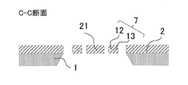
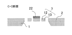
- FIG. 17 is an example of a cross-sectional view taken along a line CC in FIG. 16.
- FIG. 17 is an example of a cross-sectional view taken along a line CC in FIG. 16.
- FIG. 20 is a cross-sectional view taken along line DD of FIG.
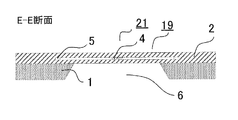
- FIG. 20 is a cross-sectional view taken along the line EE of FIG. It is a top view of the electromagnetic wave detector in Embodiment 9 of this invention.
- the present invention may include, for example, ultraviolet light and near infrared light. It is also effective to use a detector in a radio wave region such as a terahertz (THz) wave or a microwave. In the embodiment of the present invention, these lights and radio waves are collectively referred to as electromagnetic waves.
- a visible light or infrared light detector is used as the electromagnetic wave detector.
- the present invention may include, for example, ultraviolet light and near infrared light. It is also effective to use a detector in a radio wave region such as a terahertz (THz) wave or a microwave.
- THz terahertz
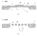
- FIG. 1 is a top view of an electromagnetic wave sensor 110 which is a prerequisite technology of the present invention.
- 2 is a cross-sectional view of the electromagnetic wave sensor 110
- FIG. 2 (a) is a cross-sectional view taken along line II in FIG. 1
- FIG. 2 (b) is a cross-sectional view taken along line II-II in FIG. .
- the illustration of the insulating film 2 on the substrate 1 is omitted for easy understanding, and the electromagnetic wave absorber 3 provided on the hot junction 4 is shown through.
- the electromagnetic wave sensor 110 includes a substrate 1 made of silicon or the like, a light receiving unit 18 that detects electromagnetic waves by converting them into heat, and a light receiving unit (temperature sensor unit) 18 held on the substrate 1 in a hollow state.
- Support legs for example, wiring or thermocouple
- An insulating film 2 made of, for example, SiO 2 or SiN is provided on the surface of the substrate 1.
- thermopile thermoelectric stack: a plurality of thermocouples connected in series to increase the output voltage
- a thing including the insulating film 2 and the thermopile 7 (thermocouple) inside thereof is called a support leg 19.
- the support leg 19 also has an effect of thermally insulating by holding the light receiving portion 18 in a hollow state and floating.
- the thermocouple includes a pair of a thermocouple material a12 and a thermocouple material b13.
- a thermocouple material a12 and a thermocouple material b13 For example, an aluminum film can be used as the thermocouple material a12 and a polysilicon film can be used as the thermocouple material b13.
- the thermocouple material a12 and the thermocouple material b13 are arranged symmetrically along the central axis 50, and one end of the thermocouple material a12 and the thermocouple material b13 is connected in the vicinity of the central axis 50.
- a hot junction 4 is formed. On the hot junction 4, that is, on the incident side of the electromagnetic wave, a light receiving unit 18 including an electromagnetic wave absorber 3 that absorbs an electromagnetic wave in a predetermined wavelength band is provided.
- the electromagnetic wave absorber 3 is disposed so as to cover the hot junction 4.
- a device including the insulating film 2 and the electromagnetic wave absorber 3 disposed thereon is referred to as a light receiving unit 18. Since the electromagnetic wave absorber 3 is not provided on the support leg 19, the surface of the support leg 9 is exposed to electromagnetic waves.
- the substrate 1 below the light receiving unit 18 is removed, and a cavity 6 is formed.
- the electromagnetic wave sensor 110 has a hollow structure in which the support leg 19 holds the light receiving unit 18 above the cavity 6.
- thermocouple material a12 and the thermocouple material b13 are connected on the substrate 1 outside the cavity 6 to form the cold junction 5. That is, the cold junction 5 is disposed in a region where the cavity 6 is not formed on the substrate 1.
- thermocouples formed at remote locations on the substrate 1 are connected by wiring 10.
- the electromagnetic wave sensor 110 when the electromagnetic wave absorber 3 absorbs electromagnetic waves, the temperature of the hot junction 4 rises, a temperature difference is generated between the hot junction 4 and the cold junction 5, and an electromotive force is generated by the Seebeck effect. .
- this electromotive force By detecting this electromotive force from the output pad 11 via the wiring 10, it is possible to detect an electromagnetic wave having a predetermined wavelength incident on the electromagnetic wave absorber 3.
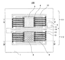
- FIG. 3 is a top view of the electromagnetic wave detector 100 according to the first exemplary embodiment of the present invention.
- 4 is a cross-sectional view taken along line IV-IV in FIG.
- FIG. 5 is a cross-sectional view taken along line VV in FIG.
- the description of the insulating film 2 on the substrate 1 is omitted, and the electromagnetic wave absorber 8 and the reflective film 9 provided on the hot junction 4 are seen through. ing.
- the electromagnetic wave detector 100 includes a first electromagnetic wave sensor 111 and a second electromagnetic wave sensor 112 which are disposed adjacent to each other on the substrate 1.
- the first electromagnetic wave sensor 111 and the second electromagnetic wave sensor 112 are connected by a wiring 14.
- the light receiving unit 18 of the first electromagnetic wave sensor 111 has a reflective film 9, and the reflective film 9 is disposed so as to cover the hot junction 4 of the thermocouple provided on the insulating film 2.
- the light receiving unit 18 of the second electromagnetic wave sensor 112 includes an electromagnetic wave absorber 8 that detects light in a predetermined wavelength range, and the electromagnetic wave absorber 8 is disposed so as to cover the hot junction 4.
- Other structures of the first electromagnetic wave sensor 111 and the second electromagnetic wave sensor 112 are the same as those of the base electromagnetic wave sensor 110 described with reference to FIGS. Further, the support legs 19 of the first electromagnetic wave sensor 111 and the second electromagnetic wave sensor 112 have the same structure.
- the electromagnetic wave absorber 8 of the second electromagnetic wave sensor 112 has a periodic structure arranged in an array on the surface so as to induce surface plasmons that couple incident light of a specific wavelength to the surface.
- the absorption amount of incident light having a specific wavelength is configured to be larger than the absorption amount of incident light having a wavelength other than the specific wavelength.
- the electromagnetic wave absorber 8 of the second electromagnetic wave sensor 112 is made of a metal such as Au or Ag.
- the thickness of the metal may be any thickness as long as the incident electromagnetic wave does not pass through the metal. As a guideline, it may be at least twice the skin thickness at the target wavelength. In the electromagnetic wave wavelength range, the film thickness is about several tens of nm to several hundreds of nm.
- the structure of the electromagnetic wave absorber 8 may be a structure in which the surface is covered with a metal that generates surface plasmons, and periodic irregularities are arranged one-dimensionally or two-dimensionally. In this case, the absorption wavelength is determined by the period of the unevenness.
- the structure of the electromagnetic wave absorber 8 may be a structure in which an insulating layer such as silicon oxide is formed on a flat metal, and a periodic isolated metal pattern is arranged one-dimensionally or two-dimensionally thereon. In this case, the absorption wavelength is determined by the size of the isolated metal pattern.
- surface plasmon When using surface plasmon for electromagnetic wave detection, it is preferable to use Au, Ag, Al or the like as the metal material of the electromagnetic wave absorber 8.
- the effects referred to as surface plasmon, pseudo surface plasmon, or metamaterial are the same from the viewpoint of wavelength selection effect due to the periodic structure of metal, and are therefore collectively referred to as “surface plasmon”.
- the electromagnetic wave absorber 8 may be a single layer structure of a metal film, a multilayer film structure of a metal film and a dielectric, or a structure in which an absorption wavelength is controlled by a dielectric multilayer film, or a material used for the electromagnetic wave absorber 8 It is also possible to use a structure in which the absorption wavelength is controlled by changing.
- the reflective film 9 is made of a metal having a flat surface and having a high reflectance in the electromagnetic wave wavelength region such as Au, Ag, and Al.
- the wiring 14 connects between the cold junction 5 of the thermocouple material a12 of the first electromagnetic wave sensor 111 and the cold junction 5 of the thermocouple material a12 of the second electromagnetic wave sensor 112.
- the operation in the case of such connection will be described.
- FIG. 6A is a schematic diagram showing the principle of a thermocouple.
- FIG. 6B is a schematic diagram showing a state in which two thermocouples are connected in the same manner as the electromagnetic wave detector 100 of the present embodiment.
- an electromotive force V is generated due to a temperature difference between the hot junction 4 and the cold junction 5.
- thermocouple materials b13 of the left and right thermocouples are connected in series as in the electromagnetic wave detector 100 of the present embodiment, the connection method for outputting the difference is basically the same. Is the same as FIG. 6 (b).
- the difference between the two sensors is obtained as the output. That is, a value obtained by subtracting the output of the first electromagnetic wave sensor 111 from the output of the second electromagnetic wave sensor 112 is obtained as the output.
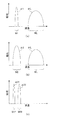
- FIG. 7A shows an ideal absorption characteristic in an electromagnetic wave sensor in which wavelength sensitivity is given to sensitivity by forming an electromagnetic wave absorber 8 that absorbs light in a predetermined wavelength range.
- FIG. 7B shows the absorption characteristics of the second electromagnetic wave sensor 112 of the electromagnetic wave detector 100 according to the first exemplary embodiment.
- the sensor output is obtained only from absorption ⁇ 2 by the electromagnetic wave absorber 8.
- the total absorption is obtained by combining the absorption ⁇ 2 by the electromagnetic wave absorber 8 in the wavelength band W2 and the absorption ⁇ L of the support leg 19 in the wavelength band WL. ⁇ . That is, the actual sensor output includes an output by the absorption ⁇ L of the support leg 19 in the wavelength band WL.
- the insulating film 2 is made of SiO 2 or SiN
- the material itself absorbs light in the vicinity of 10 ⁇ m, and this absorption is reflected in the output of the sensor.
- the absorption of the support leg itself has not been a problem.
- the intrinsic absorption of the material of the support leg itself deteriorates the wavelength selectivity and becomes a serious problem.
- the electromagnetic wave detector 100 of the present embodiment includes a first electromagnetic wave sensor 111 having a reflective film 9 provided on the hot junction 4 and an electromagnetic wave absorption that absorbs light in a predetermined wavelength band on the hot junction 4.
- a second electromagnetic wave sensor 112 provided with a body 8 and electrically so that the sensor output (thermoelectromotive force) of the first electromagnetic wave sensor 111 is subtracted from the sensor output (thermoelectromotive force) of the second electromagnetic wave sensor 112. Connected and configured to read signals from the output pad 11.
- the electromagnetic wave detector 100 having an ideal sensor output that does not include electromagnetic wave absorption in the support leg 19 can be realized.
- the sensor output of the first electromagnetic wave sensor 111 is changed from the sensor output of the second electromagnetic wave sensor 112. By subtracting, the influence of the electromagnetic wave absorbed by the support leg 19 on the sensor output can be removed.
- the electromagnetic wave detector 100 includes the first electromagnetic wave sensor 111 having the light receiving unit 18 held hollow on the substrate 1 by the support leg 19, and the support leg 19 of the first electromagnetic wave sensor 111.
- the first electromagnetic wave sensor 111 has a light receiving portion 18 that is held hollow on the substrate 1 by a support leg 19 having the same structure, and a second electromagnetic wave sensor 112 that is provided adjacent to the first electromagnetic wave sensor 111.
- the unit 18 includes the reflective film 9, and the light receiving unit 18 of the second electromagnetic wave sensor 112 includes the electromagnetic wave absorber 8 that detects light having a predetermined wavelength range or predetermined polarization, and the output of the second electromagnetic wave sensor 112. And the output of the first electromagnetic wave sensor 111 are configured to output a difference.
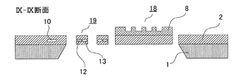
- FIG. 8A and 8B are diagrams showing a configuration of the electromagnetic wave detector 200 according to the second exemplary embodiment of the present invention.
- FIG. 8A is a top view
- FIG. 8B is a dotted circle P in FIG. It is an enlarged view of the part shown by.
- FIG. 9 is a cross-sectional view taken along line IX-IX in FIG.
- the description of the insulating film 2 on the substrate 1 is omitted, and the electromagnetic wave absorbers 8, 15, 16 and the reflective film 9 provided on the hot junction 4 are provided. It is shown in a transparent state.
- the electromagnetic wave detector 200 of the present embodiment further includes a third electromagnetic wave sensor 203 and a fourth electromagnetic wave sensor 204 that detect light in a predetermined wavelength band, as compared with the electromagnetic wave detector 100 of the first embodiment.
- a third electromagnetic wave sensor 203 and a fourth electromagnetic wave sensor 204 that detect light in a predetermined wavelength band, as compared with the electromagnetic wave detector 100 of the first embodiment.
- the structure of the support leg 19 of the present embodiment is different from the structure of the support leg 19 of the first embodiment, the structure of the support leg of the electromagnetic wave sensor that takes the difference may be the same. It is not limited. Further, the same structure includes a case where they are arranged symmetrically like the first electromagnetic wave sensor 201 and the second electromagnetic wave sensor 202 shown in FIG.
- the structure of the electromagnetic wave detector 200 of the present embodiment will be described.
- the second electromagnetic wave sensor 202 for detecting light of a predetermined wavelength band the third electromagnetic wave sensor 203
- the fourth electromagnetic wave sensor 204 are mounted on the substrate 1.
- a plurality are arranged adjacent to each other.
- the light receiving unit 18 of the first electromagnetic wave sensor 201 has a reflective film 9, and the reflective film 9 is disposed so as to cover the hot junction 4.
- the light receiving unit 18 of the second electromagnetic wave sensor 202 has an electromagnetic wave absorber 8 in the detection wavelength band ⁇ ⁇ b> 1, and the electromagnetic wave absorber 8 is disposed so as to cover the hot junction 4.
- the light receiving unit 18 of the third electromagnetic wave sensor 203 has an electromagnetic wave absorber 15 in the detection wavelength band ⁇ ⁇ b> 2, and the electromagnetic wave absorber 15 is disposed so as to cover the hot junction 4.
- the light receiving unit 18 of the fourth electromagnetic wave sensor 204 has an electromagnetic wave absorber 16 having a detection wavelength band ⁇ 3, and the electromagnetic wave absorber 16 is disposed so as to cover the hot junction 4.
- the electromagnetic wave absorbers 8, 15 and 16 are provided with concave portions in an array, for example.
- the recesses are arranged at equal intervals, and the period (pitch) is set to be approximately the same as the wavelength (specific wavelength) of the electromagnetic wave to be detected. Further, the depth of the recess is preferably about one quarter of the specific wavelength that is the wavelength to be detected, for example.
- the shape of the recess is preferably a square (plane) with a side of 3 ⁇ m, the depth is 1.5 ⁇ m, and the interval between the recesses is preferably 5 ⁇ m.
- the period (pitch) of the recess is 5 ⁇ m, which is the same as the detection wavelength.
- the planar shape of the recess may be circular.
- First, second, third, and second electromagnetic wave sensors 201 provided with a reflective film 9 on the hot junction 4 and electromagnetic wave absorbers 8, 15, and 16 that absorb light of a predetermined wavelength band on the hot junction 4 are provided.
- the four electromagnetic wave sensors 202, 203, and 204 are obtained by subtracting the sensor output (thermoelectromotive force) of the first electromagnetic wave sensor 201 from the sensor outputs (thermal electromotive force) of the second, third, and fourth electromagnetic wave sensors 202, 203, and 204.
- the wirings 17 are electrically connected to each other.
- connection part between the first electromagnetic wave sensor 201 and the second, third, and fourth electromagnetic wave sensors 202, 203, and 204 is shared, and the output of the first electromagnetic wave sensor 201 and the second, third, and fourth parts.
- the sensor outputs of the electromagnetic wave sensors 202, 203, and 204 are calculated, and signals corresponding to the detection wavelength bands ⁇ 1, ⁇ 2, and ⁇ 3 are output from the output pad.
- the electromagnetic wave detector 200 of the present embodiment includes the first electromagnetic wave sensor 201 having the light receiving unit 18 held hollow on the substrate 1 by the support leg 19, and the support leg 19 of the first electromagnetic wave sensor 201.
- the support leg 19 having the same structure has the light receiving portion 18 held hollow on the substrate 1, the second electromagnetic wave sensor 202 provided adjacent to the first electromagnetic wave sensor 201, and the support leg 19 of the first electromagnetic wave sensor 201.
- the third electromagnetic wave sensor 203 provided adjacent to the second electromagnetic wave sensor 202, and the support leg of the first electromagnetic wave sensor 201.
- the first electromagnetic wave sensor 201 includes a light receiving portion 18 that is hollowly held on the substrate 1 by the support leg 19 having the same structure as that of the first electromagnetic wave sensor 19, and a fourth electromagnetic wave sensor 204 that is provided adjacent to the third electromagnetic wave sensor 203.
- the light unit 18 includes the reflective film 9, and the light receiving units 18 of the second electromagnetic wave sensor 202, the third electromagnetic wave sensor 203, and the fourth electromagnetic wave sensor 204 detect light having different predetermined wavelength ranges or predetermined polarizations.
- the electromagnetic wave absorbers 8, 15, and 16 are configured to output a difference between the output of the second electromagnetic wave sensor 202, the third electromagnetic wave sensor 203, and the fourth electromagnetic wave sensor 204 and the output of the first electromagnetic wave sensor 201. .
- the output of the second electromagnetic wave sensor 202, the third electromagnetic wave sensor 203, and the fourth electromagnetic wave sensor 204 can be pulled out by sensor absorption due to electromagnetic wave absorption by the support leg 19 that holds the light receiving unit 18 in a hollow state.
- Wavelength selectivity of electromagnetic wave sensitivity in a predetermined wavelength range by the electromagnetic wave sensor is improved.
- the electromagnetic wave detector 200 can be reduced in size by sharing the connection portion of the wiring 17.
- the configuration having the three electromagnetic wave sensors corresponding to the detection wavelength bands ⁇ 1, ⁇ 2, and ⁇ 3 has been described.
- the electromagnetic wave sensor including the electromagnetic wave absorber 8 that detects light in a predetermined wavelength range is used.
- the number of electromagnetic wave sensors is not limited to this as long as it has a plurality of structures.
- the output of the electromagnetic wave absorber 8 and the support leg 19 is combined and the polarization selectivity is deteriorated.
- the method of eliminating the absorption of the support leg 19 by the difference is also effective for enhancing the polarization selectivity.
- the structure of the electromagnetic wave absorber 8 that detects specific polarized light is realized by changing the shape of the unevenness periodically arranged to an ellipse or a rectangle in the light receiving unit 18 using the surface plasmon described in the first embodiment. it can. Moreover, it is good also as the groove
- the shape of the metal pattern may be a highly asymmetric shape such as a rectangle or an ellipse.
- the electromagnetic wave absorber 8 is a dielectric multilayer film
- polarization selectivity can be realized if the dielectric multilayer film has a concavo-convex structure formed periodically in a one-dimensional manner.
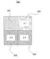
- FIG. 10 is a diagram showing a configuration of the electromagnetic wave detector 300 according to the fourth exemplary embodiment of the present invention.
- the hot junction 4 is covered with the electromagnetic wave absorbers 8, 15, and 16 corresponding to the detection wavelength bands ⁇ 1, ⁇ 2, and ⁇ 3, respectively, and detects light in a predetermined wavelength band.
- a configuration has been described in which a plurality of four electromagnetic wave sensors 202, 203, and 204 are arranged adjacent to each other in the one-dimensional direction as shown in FIG.
- the second, third, and fourth electromagnetic wave sensors 302, 303, and 304 that detect light in a specific wavelength band are reflected on the hot junction 4 as shown in FIG.
- the sensor output can be pulled out by the adjacent electromagnetic wave sensors by absorbing the electromagnetic waves at the support legs 19 that hold the light receiving unit 18 in a hollow state. Therefore, the outputs of the first electromagnetic wave sensor 301 and the outputs of the other electromagnetic wave sensors can be obtained.
- the wiring 17 to be connected is shortened. As a result, the wavelength selectivity of electromagnetic wave sensitivity in an arbitrary wavelength region by a plurality of electromagnetic wave sensors is improved, and when the electromagnetic wave detector 300 having this configuration is arranged in a two-dimensional array, the electromagnetic wave sensors 302, 303, and 304 Each can be arranged at an equal pitch.
- Embodiment 5 The structure of the electromagnetic wave detector concerning Embodiment 5 of this invention is demonstrated.
- the present embodiment is different from the first embodiment in the characteristics of the reflective film 9 provided on the hot junction of the first electromagnetic wave sensor.
- the reflective film 9 is provided on the hot contact point 4 of the first electromagnetic wave sensor 111.
- the reflection film 9 that reflects light having a wavelength other than the specific wavelength range W1 included in the wavelength range W2 of the light detected by the electromagnetic wave absorber 8 of the second electromagnetic wave sensor 112 is provided.
- the reflective film 9 absorbs light of the specific wavelength W1 included in the wavelength range W2 of light detected by the electromagnetic wave absorber 8 of the second electromagnetic wave sensor 112, and reflects light of other wavelengths. Therefore, the sensor output of the first electromagnetic wave sensor 111 includes the sensor output (thermoelectromotive force) by absorbing the specific wavelength range.
- the first electromagnetic wave sensor 111 including the reflective film 9 that reflects light other than the specific wavelength band W1 and the second electromagnetic wave sensor 112 including the electromagnetic wave absorber 8 that absorbs light in the specific wavelength band W2 are the second Electrical connection is made so that the sensor output (thermoelectromotive force) of the first electromagnetic wave sensor 111 is subtracted from the sensor output (thermoelectromotive force) of the electromagnetic wave sensor 112. The subtracted sensor output is read from the output pad 11 as a signal.
- FIG. 11 is a diagram illustrating the absorption characteristics of the electromagnetic wave detector according to the fourth embodiment.
- 11A shows the absorption characteristic of the first electromagnetic wave sensor 111
- FIG. 11B shows the absorption characteristic of the second electromagnetic wave sensor 112
- FIG. 11C shows the absorption characteristic of the electromagnetic wave detector.
- Absorption ⁇ L of leg 19 occurs.
- the absorption ⁇ 2 of the electromagnetic wave absorber 8 in the wavelength band W2 and the wavelength band Absorption ⁇ L of the support leg 19 in WL occurs.
- the wavelength band W1 is included in the range of the wavelength band W2.
- the differential between the first electromagnetic wave sensor 111 and the second electromagnetic wave sensor 112 is output, the influence of the absorption ⁇ L of the support leg 19 is canceled, and the final output is the electromagnetic wave absorber 8 of the second electromagnetic wave sensor 112. Is the difference between the sensor output due to the absorption ⁇ 2 and the sensor output due to the absorption ⁇ 1 of the reflective film 9 of the first electromagnetic wave sensor 111.
- the output of the electromagnetic wave detector of the present embodiment is obtained from the absorption ⁇ 21, ⁇ 22 at two different wavelengths W21, W22 as shown in FIG. can get. That is, the electromagnetic wave detector of the present embodiment is equivalent to having sensitivity to the two wavelengths W21 and W22.
- the wavelength-selective electromagnetic wave absorber 8 having a different half width the following structures are conceivable. For example, in the case of a structure in which irregularities are arranged two-dimensionally, changing the ratio between the arrangement period of the irregularities and the size of the concave part changes the monochromaticity of the resonance wavelength, so the half-value width of the absorption wavelength is changed. Can do. In addition, it is possible to control the half width by changing the metal material. For example, since the loss of nickel and the like is larger than that of gold or silver, the full width at half maximum is increased.
- the electromagnetic wave detector By configuring the electromagnetic wave detector as described above, it is possible to draw a sensor output by electromagnetic wave absorption at the support leg 19 holding the light receiving unit 18 in a hollow manner, or a sensor output of optical information in an unnecessary wavelength region. Wavelength selectivity of electromagnetic wave sensitivity is improved.
- FIG. 12 is a diagram showing a schematic configuration of the gas analyzer 400.
- gas has absorption peaks at a plurality of wavelengths centering on the infrared wavelength region. That is, if the absorption peak can be identified for a certain gas, the type of the gas can be determined.
- the gas analyzer 400 of this embodiment uses this property to determine the type of gas, and introduces a light source 20 that emits electromagnetic waves (in this embodiment, infrared rays) and a gas to be analyzed.
- an electromagnetic wave detector hereinafter also referred to as a differential infrared sensor array 40 shown in the first to fifth embodiments of the present invention.
- the electromagnetic wave L1 emitted from the light source 20 passes through the gas in the gas introduction mechanism 30, and the electromagnetic wave L2 after passing through the gas is differential. It is arranged so as to be incident on the mold infrared sensor array 40.
- the differential infrared sensor array 40 detects the intensity of an electromagnetic wave having a specific wavelength contained in the electromagnetic wave L2 that has passed through the gas to be analyzed.
- the gas introduction mechanism 30 is a container that contains a gas to be analyzed. As shown in FIG. 12, when the light source 20, the gas introduction mechanism 30, and the differential infrared sensor array 40 are arranged in this order, the electromagnetic wave L ⁇ b> 1 radiated from the light source 20 passes through the gas introduction mechanism 30 and the differential. A window that is incident on the infrared sensor array 40 is installed. Alternatively, the light source 20 and the differential infrared sensor array 40 may be installed in the gas introduction mechanism 30.
- the intensity of the electromagnetic wave at the gas absorption wavelength is attenuated according to the gas concentration. Therefore, by setting a plurality of wavelengths that can be detected by the differential infrared sensor array 40, the absorption wavelength of gas, that is, the type of gas, can be specified from the output of the differential infrared sensor array 40.
- the gas analyzer 400 can be applied to, for example, an apparatus that detects carbon dioxide, alcohol that discriminates alcohol, or the like from a gas to be analyzed.
- an uncooled infrared sensor is used as the differential infrared sensor array 40 of these gas analyzers 400, the absorption of the support legs is output, so accurate analysis is difficult. Wavelength analysis becomes possible. It is also possible to mount a plurality of sensors having a detection wavelength corresponding to the gas type in one element, and the gas analyzer itself can be made small and simple.
- the electromagnetic wave detector and gas analyzer that excludes the sensor output due to absorption of the support legs described above are similarly effective even when other thermal electromagnetic wave sensors such as a bolometer, pyroelectric type, SOI diode type, etc. are used. .
- FIG. 13 is a top view of the electromagnetic wave detector 120 according to the seventh exemplary embodiment of the present invention.
- Each electromagnetic wave sensor includes a substrate 1 made of silicon or the like, a light receiving unit 18 that detects electromagnetic waves by converting them into heat, and a support leg (for example, a wiring or a thermocouple) that holds the light receiving unit (temperature sensor unit) 18 on the substrate 1 in a hollow state. ) 19.
- An insulating film 2 made of, for example, SiO 2 or SiN is provided on the surface of the substrate 1.
- a thermopile thermoelectric stack: a plurality of thermocouples connected in series to increase the output voltage
- the output voltage increases as the number of thermocouples increases.
- the greater the number of thermocouples the easier the escape of heat from the hot junction 4 region to the substrate 1.
- the thing including the insulating film 2 and the thermopile 7 (thermocouple) inside thereof is referred to as a support leg 19.
- the support leg 19 also has an effect of thermally insulating by holding the light receiving portion 18 in a hollow state and floating.
- the configuration of the electromagnetic wave detector 120 according to the seventh embodiment of the present invention will be described.
- the electromagnetic wave detector 120 includes two electromagnetic wave sensors described as the prerequisite technology.
- the two electromagnetic wave sensors 113 and 114 differ in the configuration of the light receiving unit 18.
- FIG. 13 is a top view of the electromagnetic wave detector 120 according to the seventh exemplary embodiment of the present invention.
- FIG. 14 is a cross-sectional view taken along line AA in FIG.
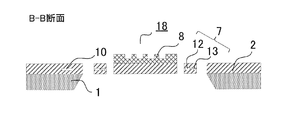
- FIG. 15 is a sectional view taken along line BB in FIG.
- the description of the insulating film 2 on the substrate 1 is omitted, and the electromagnetic wave absorber 8 and the reflective film 9 provided on the hot junction 4 are seen through. ing.
- the electromagnetic wave detector 120 includes a first electromagnetic wave sensor 113 and a second electromagnetic wave sensor 114 which are disposed adjacent to each other on the substrate 1.
- the first electromagnetic wave sensor 113 and the second electromagnetic wave sensor 114 are connected by the wiring 14.
- the light receiving portion 18 of the first electromagnetic wave sensor 113 has a reflective film 9, and the reflective film 9 is disposed so as to cover the hot junction 4 of the thermocouple provided on the insulating film 2.
- the light receiving unit 18 of the second electromagnetic wave sensor 114 includes an electromagnetic wave absorber 8 that detects light in a predetermined wavelength range, and the electromagnetic wave absorber 8 is disposed so as to cover the hot junction 4.
- Other structures of the first electromagnetic wave sensor 113 and the second electromagnetic wave sensor 114 are the same as those of the premise electromagnetic wave sensor 110 described with reference to FIGS. Further, the support legs 19 of the first electromagnetic wave sensor 113 and the second electromagnetic wave sensor 114 have the same structure.
- a first electromagnetic wave sensor 113 having a reflective film 9 provided on the hot junction 4 and an electromagnetic wave absorber 8 for absorbing light in a predetermined wavelength band are provided on the hot junction 4.
- the electromagnetic wave detector 120 having an ideal sensor output that does not include electromagnetic wave absorption in the support leg 19 can be realized.
- the sensor output of the first electromagnetic wave sensor 113 is changed from the sensor output of the second electromagnetic wave sensor 114.
- the influence of the electromagnetic wave absorbed by the support leg 19 on the sensor output can be removed.
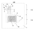
- the electromagnetic wave detector 130 including the second electromagnetic wave sensor 116 provided with the absorber 8 the electromagnetic wave detector 130 having an ideal sensor output that does not include the absorption of the electromagnetic wave in the support leg 19 can be realized. Thereby, the area of the electromagnetic wave detector can be reduced.
- the electromagnetic wave detector 130 is hollow on the substrate 1 by the support leg 19 having the same structure as the support leg 19 of the fifth electromagnetic wave sensor 115 in which the support leg 19 is held hollow on the substrate 1.
- a second electromagnetic wave sensor 116 that is provided adjacent to the fifth electromagnetic wave sensor 115 and has the light receiving part 18 held; the fifth electromagnetic wave sensor 115 has no light receiving part 18;
- the hot junction 4 of the thermocouple is thermally connected in the hot junction region 21 formed of the insulating film 2, and the light receiving unit 18 of the second electromagnetic wave sensor 116 is
- the electromagnetic wave absorber 8 detects light having a predetermined wavelength range or predetermined polarization, and is configured to output a difference between the output of the second electromagnetic wave sensor 116 and the output of the fifth electromagnetic wave sensor 115.
- the insulating film 2 in the hot junction region 21 may be omitted.
- the reflective film 22 made of a material having a large specific heat is heated. You may form in the contact area 21.
- the output of the second electromagnetic wave sensor 116 can subtract the sensor output due to electromagnetic wave absorption at the support leg 19 that holds the light receiving unit 18 in a hollow state, the wavelength selectivity of the electromagnetic wave sensitivity is improved.
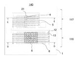
- FIG. 19 is a top view of the electromagnetic wave detector 140 according to the eighth exemplary embodiment of the present invention.
- 20 is a cross-sectional view taken along the line DD of FIG.
- FIG. 21 is a cross-sectional view taken along line EE in FIG.
- the description of the insulating film 2 on the substrate 1 is omitted, and the electromagnetic wave absorber 8 provided on the hot junction 4 is seen through.
- thermopile thermoelectric stack: a thermopile composed of a plurality of thermocouples is formed on the insulating film 2 of the fifth electromagnetic wave sensor 117 and the second electromagnetic wave sensor 118 arranged adjacent to each other on the substrate 1.
- thermoelectric stack a thermopile composed of a plurality of thermocouples is formed on the insulating film 2 of the fifth electromagnetic wave sensor 117 and the second electromagnetic wave sensor 118 arranged adjacent to each other on the substrate 1.
- a large number of thermocouples connected in series to increase the output voltage) 7 is provided. The output voltage increases as the number of thermocouples increases.
- FIG. 22 is a diagram showing the configuration of the electromagnetic wave detector 210 according to the ninth embodiment of the present invention.
- the insulating film 2 on the substrate 1 is shown for easy understanding. Omitted, the electromagnetic wave absorbers 8, 15 and 16 provided on the hot junction 4 are shown in a transparent state.
- the electromagnetic wave detector 210 according to the present embodiment further includes a third electromagnetic wave sensor 207 and a fourth electromagnetic wave sensor 208 that detect light in a predetermined wavelength band as compared with the electromagnetic wave detector 120 according to the seventh embodiment. Is different. Since the other configuration is the same as that of the seventh embodiment, the following description focuses on the configuration unique to this embodiment.
- the structure of the support leg 19 of the present embodiment is different from the structure of the support leg 19 of the seventh embodiment, the structure, width, and length of the support leg of the electromagnetic wave sensor that takes the difference may be the same.
- the structure is not particularly limited.
- the structure of the electromagnetic wave detector 210 of the present embodiment will be described.
- the fifth electromagnetic wave sensor 205 without the light receiving unit 18, the second electromagnetic wave sensor 206 for detecting light of a predetermined wavelength band, the third electromagnetic wave sensor 207, the fourth electromagnetic wave sensor 208, and adjacent to each other on the substrate 1. A plurality of them are arranged.
- the fifth electromagnetic wave sensor 205 does not have the light receiving unit 18.
- the light receiving unit 18 of the second electromagnetic wave sensor 206 has an electromagnetic wave absorber 8 in the detection wavelength band ⁇ 1, and the electromagnetic wave absorber 8 is disposed so as to cover the hot junction 4.
- the light receiving unit 18 of the third electromagnetic wave sensor 207 has an electromagnetic wave absorber 15 in the detection wavelength band ⁇ ⁇ b> 2, and the electromagnetic wave absorber 15 is disposed so as to cover the hot junction 4.
- the light receiving unit 18 of the fourth electromagnetic wave sensor 208 has the electromagnetic wave absorber 16 in the detection wavelength band ⁇ 3, and the electromagnetic wave absorber 16 is disposed so as to cover the hot junction 4.
- the electromagnetic wave detector 210 of the present embodiment is hollowly held on the substrate 1 by a fifth electromagnetic wave sensor 205 constituted by only the support leg 19 and a support leg 19 having the same structure as the support leg 19 of the fifth electromagnetic wave sensor 205.
- the second electromagnetic wave sensor 206 provided adjacent to the fifth electromagnetic wave sensor 205 and the support leg 19 having the same structure as the support leg 19 of the fifth electromagnetic wave sensor 205 is held hollow on the substrate 1.
- the third electromagnetic wave sensor 207 provided adjacent to the second electromagnetic wave sensor 206 and the support leg 19 having the same structure as the support leg 19 of the fifth electromagnetic wave sensor 205 are hollow on the substrate 1.
- a fourth electromagnetic wave sensor 208 provided adjacent to the third electromagnetic wave sensor 207.
- the second electromagnetic wave sensor 206, the third electromagnetic wave sensor 207, and the fourth electromagnetic wave sensor 2 are provided.
- 8 light receiving units 18 have electromagnetic wave absorbers 8, 15, and 16 that detect light having different predetermined wavelength ranges or predetermined polarizations, respectively, and include a second electromagnetic wave sensor 206, a third electromagnetic wave sensor 207, and a fourth electromagnetic wave sensor. A difference between the output of 208 and the output of the fifth electromagnetic wave sensor 205 is output.
- the sensor output by the electromagnetic wave absorption by the support leg 19 can be pulled from the outputs of the second electromagnetic wave sensor 206, the third electromagnetic wave sensor 207, and the fourth electromagnetic wave sensor 208, and a predetermined wavelength range by a plurality of electromagnetic wave sensors can be obtained.
- the wavelength selectivity of the electromagnetic wave sensitivity is improved.
- the electromagnetic wave detector 210 can be downsized by sharing the connection portion of the wiring 17.
- the configuration having the three electromagnetic wave sensors corresponding to the detection wavelength bands ⁇ 1, ⁇ 2, and ⁇ 3 has been described.
- the electromagnetic wave sensor including the electromagnetic wave absorber 8 that detects light in a predetermined wavelength range is used.
- the number of electromagnetic wave sensors is not limited to this as long as it has a plurality of structures.
Landscapes
- Physics & Mathematics (AREA)
- Health & Medical Sciences (AREA)
- Life Sciences & Earth Sciences (AREA)
- General Physics & Mathematics (AREA)
- Spectroscopy & Molecular Physics (AREA)
- Chemical & Material Sciences (AREA)
- Pathology (AREA)
- Biochemistry (AREA)
- Immunology (AREA)
- Analytical Chemistry (AREA)
- General Health & Medical Sciences (AREA)
- Engineering & Computer Science (AREA)
- Biomedical Technology (AREA)
- Molecular Biology (AREA)
- Biophysics (AREA)
- Hematology (AREA)
- Urology & Nephrology (AREA)
- Food Science & Technology (AREA)
- Medicinal Chemistry (AREA)
- Investigating Or Analysing Materials By Optical Means (AREA)
- Photometry And Measurement Of Optical Pulse Characteristics (AREA)
Abstract
Priority Applications (4)
| Application Number | Priority Date | Filing Date | Title |
|---|---|---|---|
| DE112016000672.1T DE112016000672T5 (de) | 2015-02-09 | 2016-01-04 | Detektor für elektromagnetische Wellen und Gasanalyseeinrichtung |
| CN201680007199.8A CN107209057B (zh) | 2015-02-09 | 2016-01-04 | 电磁波检测器以及气体分析装置 |
| JP2016524157A JP6095856B2 (ja) | 2015-02-09 | 2016-01-04 | 電磁波検出器、及びガス分析装置 |
| US15/543,421 US10309895B2 (en) | 2015-02-09 | 2016-01-04 | Electromagnetic wave detector and gas analysis device having dual electromagnetic wave sensors for detecting one of light in a predetermined wavelength band and predetermined polarization |
Applications Claiming Priority (2)
| Application Number | Priority Date | Filing Date | Title |
|---|---|---|---|
| JP2015-022886 | 2015-02-09 | ||
| JP2015022886 | 2015-02-09 |
Publications (1)
| Publication Number | Publication Date |
|---|---|
| WO2016129293A1 true WO2016129293A1 (fr) | 2016-08-18 |
Family
ID=56614557
Family Applications (1)
| Application Number | Title | Priority Date | Filing Date |
|---|---|---|---|
| PCT/JP2016/050027 Ceased WO2016129293A1 (fr) | 2015-02-09 | 2016-01-04 | Détecteur d'onde électromagnétique et dispositif d'analyse de gaz |
Country Status (5)
| Country | Link |
|---|---|
| US (1) | US10309895B2 (fr) |
| JP (1) | JP6095856B2 (fr) |
| CN (1) | CN107209057B (fr) |
| DE (1) | DE112016000672T5 (fr) |
| WO (1) | WO2016129293A1 (fr) |
Cited By (5)
| Publication number | Priority date | Publication date | Assignee | Title |
|---|---|---|---|---|
| EP3144663B1 (fr) * | 2016-11-18 | 2020-06-17 | Sensirion AG | Module de détecteur de gaz |
| WO2022176949A1 (fr) * | 2021-02-19 | 2022-08-25 | 国立大学法人横浜国立大学 | Détecteur à infrarouge et capteur de gaz équipé d'un détecteur à infrarouge |
| US20230055177A1 (en) * | 2021-08-20 | 2023-02-23 | Tdk Corporation | Electromagnetic wave sensor |
| US20230064502A1 (en) * | 2021-08-30 | 2023-03-02 | Tdk Corporation | Structure body and electromagnetic wave sensor |
| US12480817B2 (en) | 2021-08-30 | 2025-11-25 | Tdk Corporation | Structure body and electromagnetic wave sensor |
Families Citing this family (6)
| Publication number | Priority date | Publication date | Assignee | Title |
|---|---|---|---|---|
| CN110462377A (zh) * | 2016-12-09 | 2019-11-15 | 新加坡国立大学 | 气体传感器mems结构及其制造方法 |
| EP3421947B1 (fr) | 2017-06-30 | 2019-08-07 | Sensirion AG | Procédé de fonctionnement d'un dispositif de capteur de débit |
| CN109799202B (zh) * | 2019-01-16 | 2023-11-24 | 黄文佳 | 一种利用电磁波反射成像图进行物质分析的装置及方法 |
| US11313741B2 (en) * | 2019-12-11 | 2022-04-26 | Apple Inc. | Packaging technologies for temperature sensing in health care products |
| CN112577612B (zh) * | 2020-12-09 | 2022-04-08 | 中国电子科技集团公司第四十四研究所 | 黑硅等离激元辅助吸收的热电堆芯片及其制作方法 |
| JP2022165185A (ja) | 2021-04-19 | 2022-10-31 | 国立大学法人 東京大学 | センサ素子及びセンサ装置 |
Citations (4)
| Publication number | Priority date | Publication date | Assignee | Title |
|---|---|---|---|---|
| JPH11258040A (ja) * | 1998-03-12 | 1999-09-24 | Omron Corp | サーモパイル型赤外線センサ |
| JP2013195148A (ja) * | 2012-03-16 | 2013-09-30 | Ricoh Co Ltd | 赤外線センサー装置 |
| JP2014032088A (ja) * | 2012-08-02 | 2014-02-20 | Mitsubishi Electric Corp | 電磁波センサ及び電磁波センサ装置 |
| JP2014081261A (ja) * | 2012-10-16 | 2014-05-08 | Ngk Spark Plug Co Ltd | ガス濃度検出装置 |
Family Cites Families (16)
| Publication number | Priority date | Publication date | Assignee | Title |
|---|---|---|---|---|
| US2898800A (en) * | 1954-07-23 | 1959-08-11 | Bergson Gustav | Gas analyzing system of the radiant energy absorption type |
| JP3809718B2 (ja) * | 1997-12-26 | 2006-08-16 | 日産自動車株式会社 | 赤外線検知素子 |
| JP3409848B2 (ja) | 2000-08-29 | 2003-05-26 | 日本電気株式会社 | 熱型赤外線検出器 |
| JP4241360B2 (ja) | 2003-12-15 | 2009-03-18 | 株式会社デンソー | 赤外線センサの製造方法 |
| JP2005249764A (ja) * | 2004-03-02 | 2005-09-15 | Katsumi Mori | 物体色測定方式 |
| CN1619295A (zh) * | 2004-12-10 | 2005-05-25 | 南京农业大学 | 猪肉颜色分级仪 |
| US7692148B2 (en) | 2005-01-26 | 2010-04-06 | Analog Devices, Inc. | Thermal sensor with thermal barrier |
| DE102007013124A1 (de) | 2006-10-20 | 2008-04-24 | Johnson Controls Gmbh | Vorrichtung und Verfahren zur Bedienung eines Kraftfahrzeuges |
| JP2010127739A (ja) * | 2008-11-27 | 2010-06-10 | Toppan Printing Co Ltd | 分光感度特性測定装置および分光感度特性測定方法 |
| CN102575983A (zh) | 2009-06-25 | 2012-07-11 | 松下电器产业株式会社 | 红外线式气体检测器以及红外线式气体测量装置 |
| JP5374297B2 (ja) | 2009-06-25 | 2013-12-25 | パナソニック株式会社 | 赤外線式ガス検知器および赤外線式ガス計測装置 |
| CN201534392U (zh) * | 2009-07-16 | 2010-07-28 | 上海理工大学 | 药片冲压设备高精度检测系统 |
| JP4964935B2 (ja) | 2009-10-30 | 2012-07-04 | 三菱電機株式会社 | 半導体光素子および半導体光装置 |
| JP5425127B2 (ja) | 2011-03-09 | 2014-02-26 | 株式会社東芝 | 固体撮像素子 |
| JP2014032068A (ja) | 2012-08-02 | 2014-02-20 | Koptic Inc | ガス濃度測定装置 |
| JP2014163674A (ja) | 2013-02-21 | 2014-09-08 | Seiko Epson Corp | テラヘルツ波検出装置、カメラ、イメージング装置、および計測装置 |
-
2016
- 2016-01-04 DE DE112016000672.1T patent/DE112016000672T5/de active Pending
- 2016-01-04 CN CN201680007199.8A patent/CN107209057B/zh active Active
- 2016-01-04 JP JP2016524157A patent/JP6095856B2/ja active Active
- 2016-01-04 US US15/543,421 patent/US10309895B2/en active Active
- 2016-01-04 WO PCT/JP2016/050027 patent/WO2016129293A1/fr not_active Ceased
Patent Citations (4)
| Publication number | Priority date | Publication date | Assignee | Title |
|---|---|---|---|---|
| JPH11258040A (ja) * | 1998-03-12 | 1999-09-24 | Omron Corp | サーモパイル型赤外線センサ |
| JP2013195148A (ja) * | 2012-03-16 | 2013-09-30 | Ricoh Co Ltd | 赤外線センサー装置 |
| JP2014032088A (ja) * | 2012-08-02 | 2014-02-20 | Mitsubishi Electric Corp | 電磁波センサ及び電磁波センサ装置 |
| JP2014081261A (ja) * | 2012-10-16 | 2014-05-08 | Ngk Spark Plug Co Ltd | ガス濃度検出装置 |
Cited By (8)
| Publication number | Priority date | Publication date | Assignee | Title |
|---|---|---|---|---|
| EP3144663B1 (fr) * | 2016-11-18 | 2020-06-17 | Sensirion AG | Module de détecteur de gaz |
| US10928312B2 (en) | 2016-11-18 | 2021-02-23 | Sensirion Ag | Gas sensor module |
| WO2022176949A1 (fr) * | 2021-02-19 | 2022-08-25 | 国立大学法人横浜国立大学 | Détecteur à infrarouge et capteur de gaz équipé d'un détecteur à infrarouge |
| US20230055177A1 (en) * | 2021-08-20 | 2023-02-23 | Tdk Corporation | Electromagnetic wave sensor |
| US12474215B2 (en) * | 2021-08-20 | 2025-11-18 | Tdk Corporation | Electromagnetic wave sensor |
| US20230064502A1 (en) * | 2021-08-30 | 2023-03-02 | Tdk Corporation | Structure body and electromagnetic wave sensor |
| US12480817B2 (en) | 2021-08-30 | 2025-11-25 | Tdk Corporation | Structure body and electromagnetic wave sensor |
| US12492942B2 (en) * | 2021-08-30 | 2025-12-09 | Tdk Corporation | Structure body and electromagnetic wave sensor |
Also Published As
| Publication number | Publication date |
|---|---|
| JP6095856B2 (ja) | 2017-03-15 |
| CN107209057A (zh) | 2017-09-26 |
| DE112016000672T5 (de) | 2017-11-09 |
| US20180003622A1 (en) | 2018-01-04 |
| US10309895B2 (en) | 2019-06-04 |
| JPWO2016129293A1 (ja) | 2017-04-27 |
| CN107209057B (zh) | 2019-08-13 |
Similar Documents
| Publication | Publication Date | Title |
|---|---|---|
| JP6095856B2 (ja) | 電磁波検出器、及びガス分析装置 | |
| US10234379B2 (en) | Electromagnetic wave detector, electromagnetic wave detector array, and gas analyzing apparatus | |
| US8629398B2 (en) | Detection beyond the standard radiation noise limit using spectrally selective absorption | |
| EP3368871B1 (fr) | Dispositif infrarouge | |
| KR101910573B1 (ko) | 광대역 광 흡수체를 포함하는 적외선 검출기 | |
| US9171885B2 (en) | Infrared detector and infrared image sensor including the same | |
| KR101922119B1 (ko) | 적외선 검출기 및 이를 사용하는 적외선 검출 방법 | |
| KR102040149B1 (ko) | 적외선 검출기 | |
| US9494469B2 (en) | Infrared detection device | |
| US7622717B2 (en) | Pixel structure having an umbrella type absorber with one or more recesses or channels sized to increase radiation absorption | |
| KR101861147B1 (ko) | 적외선 검출기 | |
| US10151638B2 (en) | Bolometer, method of fabricating the same, and bolometric method | |
| JP6548838B2 (ja) | 生体物質測定装置 | |
| JP2014190783A (ja) | 電磁波検出器およびそれを備えた撮像装置 | |
| Dem’yanenko et al. | Application of uncooled microbolometer detector arrays for recording radiation of the terahertz spectral range | |
| RU2606516C2 (ru) | Пироэлектрический детектор миллиметрового излучения (варианты) | |
| KR102040151B1 (ko) | 열 복사 센서 및 이를 포함하는 열상 촬영 장치 | |
| JP5757254B2 (ja) | 半導体光素子および半導体光装置 | |
| JP5456810B2 (ja) | 熱型赤外線検出器 | |
| JP2013253896A (ja) | 光検出素子、カメラおよび電子機器 |
Legal Events
| Date | Code | Title | Description |
|---|---|---|---|
| ENP | Entry into the national phase |
Ref document number: 2016524157 Country of ref document: JP Kind code of ref document: A |
|
| 121 | Ep: the epo has been informed by wipo that ep was designated in this application |
Ref document number: 16748938 Country of ref document: EP Kind code of ref document: A1 |
|
| WWE | Wipo information: entry into national phase |
Ref document number: 15543421 Country of ref document: US |
|
| WWE | Wipo information: entry into national phase |
Ref document number: 112016000672 Country of ref document: DE |
|
| 122 | Ep: pct application non-entry in european phase |
Ref document number: 16748938 Country of ref document: EP Kind code of ref document: A1 |