WO2016129317A1 - Structure de protection contre les décharges électrostatiques et son procédé de production - Google Patents
Structure de protection contre les décharges électrostatiques et son procédé de production Download PDFInfo
- Publication number
- WO2016129317A1 WO2016129317A1 PCT/JP2016/050812 JP2016050812W WO2016129317A1 WO 2016129317 A1 WO2016129317 A1 WO 2016129317A1 JP 2016050812 W JP2016050812 W JP 2016050812W WO 2016129317 A1 WO2016129317 A1 WO 2016129317A1
- Authority
- WO
- WIPO (PCT)
- Prior art keywords
- electrode
- heat dissipation
- pad
- unfired
- interlayer connection
- Prior art date
- Legal status (The legal status is an assumption and is not a legal conclusion. Google has not performed a legal analysis and makes no representation as to the accuracy of the status listed.)
- Ceased
Links
Images







Classifications
-
- H—ELECTRICITY
- H01—ELECTRIC ELEMENTS
- H01T—SPARK GAPS; OVERVOLTAGE ARRESTERS USING SPARK GAPS; SPARKING PLUGS; CORONA DEVICES; GENERATING IONS TO BE INTRODUCED INTO NON-ENCLOSED GASES
- H01T4/00—Overvoltage arresters using spark gaps
- H01T4/10—Overvoltage arresters using spark gaps having a single gap or a plurality of gaps in parallel
-
- H—ELECTRICITY
- H01—ELECTRIC ELEMENTS
- H01T—SPARK GAPS; OVERVOLTAGE ARRESTERS USING SPARK GAPS; SPARKING PLUGS; CORONA DEVICES; GENERATING IONS TO BE INTRODUCED INTO NON-ENCLOSED GASES
- H01T21/00—Apparatus or processes specially adapted for the manufacture or maintenance of spark gaps or sparking plugs
-
- H—ELECTRICITY
- H01—ELECTRIC ELEMENTS
- H01T—SPARK GAPS; OVERVOLTAGE ARRESTERS USING SPARK GAPS; SPARKING PLUGS; CORONA DEVICES; GENERATING IONS TO BE INTRODUCED INTO NON-ENCLOSED GASES
- H01T4/00—Overvoltage arresters using spark gaps
- H01T4/10—Overvoltage arresters using spark gaps having a single gap or a plurality of gaps in parallel
- H01T4/12—Overvoltage arresters using spark gaps having a single gap or a plurality of gaps in parallel hermetically sealed
Definitions
- the present invention relates to an electrostatic discharge protection structure for protecting an electronic device from destruction due to electrostatic discharge and a method for manufacturing the same.
- ESD protection device An electrostatic discharge protection device (ESD protection device) is widely used in order to prevent destruction or malfunction of an electronic device due to electrostatic discharge (ESD).
- Patent Document 1 has a ceramic multilayer substrate, a cavity formed inside the ceramic multilayer substrate, and a facing portion arranged so that the tips are opposed to each other with a space in the cavity.
- An ESD protection device having at least a pair of discharge electrodes and an external electrode formed on the surface of a ceramic multilayer substrate and connected to the discharge electrodes is described.
- a ceramic / metal mixed paste is applied on a ceramic green sheet by screen printing, and an electrode paste is applied on the ceramic green sheet by screen printing to form a discharge electrode having a discharge gap between opposing portions. It is described to do.
- Patent Document 2 a ceramic element body having a hollow portion therein, a portion exposed to the cavity portion, a first discharge electrode embedded in the ceramic element body; A first discharge electrode and a second discharge electrode embedded in the ceramic body, the second discharge electrode having a portion opposed to the first discharge electrode by a predetermined distance.
- the discharge electrode is made of a metal containing 80 weight percent or more of tungsten, and the amount of tungsten bonded to oxygen is 2.0 atoms relative to the total amount of tungsten in the first discharge electrode and the second discharge electrode. % Is less than or equal to%.
- Patent Document 2 describes that a metal layer is formed by screen-printing a conductive paste, and an antistatic component including a discharge electrode made of the metal layer is obtained.
- the distance between the discharge electrodes in the ESD protection device is reduced by adopting a structure in which the discharge electrodes are constituted by interlayer connection conductors arranged inside the ceramic laminate and the discharge electrodes are opposed to each other in the lamination direction of the laminate. It can be made smaller.
- the ESD protection device may be required to have high resistance against a large current depending on the application.
- an ESD protection device having higher resistance to a large current than a conventional ESD protection device can be obtained.
- the discharge electrode constituted by the interlayer connection conductor has an advantage that the distance between the discharge electrodes arranged in the ESD protection device can be reduced and the ESD protection device can be reduced in size.
- an ESD protection device is required to have excellent resistance to repeated electrostatic discharge in addition to the above-described miniaturization and resistance to a large current.
- An object of the present invention is to provide an electrostatic discharge protection structure excellent in resistance to repeated electrostatic discharge and a method for manufacturing the same.
- a first laminate portion including one or more ceramic layers including one or more interlayer connection conductors;
- a second laminated body part disposed on the first laminated body part, the second laminated body part including one or more ceramic layers including one or more interlayer connection conductors;
- a cavity portion disposed between the first laminate portion and the second laminate portion;
- a first electrode exposed region and a second electrode exposed region disposed opposite to each other inside the cavity,
- An electrostatic discharge protection structure that includes a second electrode that is disposed outside the second stacked body portion and that is electrically connected to the second electrode exposed region through an interlayer connection conductor included in the second stacked body portion.
- an area of the electrode exposed region in a plan view between the ceramic layer in which the electrode exposed region is disposed and the ceramic layer adjacent to the ceramic layer is larger than the area of the electrode exposed region.
- a heat dissipation / connection pad having a larger area is disposed, and the heat dissipation / connection pad includes an interlayer connection conductor included in a ceramic layer in which the electrode exposed region is disposed, and a ceramic layer adjacent to the ceramic layer in which the electrode exposed region is disposed.
- an electrostatic discharge protection structure for connecting an interlayer connection conductor included in the structure.
- the interlayer connection conductor included in the ceramic layer in contact with the cavity part may be exposed inside the cavity part to form an electrode exposed region.
- a counter part pad electrode is disposed on the surface of the ceramic layer in contact with the cavity so as to cover the interlayer connection conductor included in the ceramic layer.
- the surface of the counter part pad electrode may be exposed inside the cavity to form an electrode exposed region.
- At least one of the first laminate portion and the second laminate portion described above may further include one or more additional heat dissipation / connection pads arranged between adjacent ceramic layers, and the additional heat dissipation / connection pads. Connects an interlayer connection conductor included in one ceramic layer in contact with the additional heat dissipation / connection pad and an interlayer connection conductor included in the other ceramic layer in contact with the additional heat dissipation / connection pad.
- the interlayer connection conductor is made of the same material as the heat dissipation / connection pad and, if present, the counter part pad electrode and the additional heat dissipation / connection pad. May be configured.
- the interlayer connection conductor has a tapered shape in which the diameter on the side close to the second electrode is smaller than the diameter on the side close to the first electrode. You can do it.
- the interlayer connection conductor has a tapered shape in which the diameter on the side close to the first electrode is smaller than the diameter on the side close to the second electrode. You can do it.
- the interlayer connection conductor in both the first laminate portion and the second laminate portion, is a heat dissipation / connection pad and, if present, a counter portion pad electrode and Consists of the same material as the additional heat dissipation / connection pad,
- the interlayer connecting conductors included in the first stacked body part and the second stacked body part have a taper shape, and the direction from the large diameter side to the small diameter side of the interlayer connecting conductor included in the first stacked body part;
- the electrostatic discharge protection structure may be a direction in which the direction from the large diameter side to the small diameter side of the interlayer connection conductor included in the second multilayer body portion is different.
- the interlayer connection conductor included in the ceramic layer in contact with the cavity part is located inside the cavity part. Exposed to form an electrode exposed area, In both the first laminate part and the second laminate part, the interlayer connection conductor is made of the same material as the heat dissipation / connection pad and, if present, the opposing pad electrode and the additional heat dissipation / connection pad.
- the interlayer connecting conductors included in the first stacked body part and the second stacked body part have a taper shape, and the direction from the large diameter side to the small diameter side of the interlayer connecting conductor included in the first stacked body part;
- the electrostatic discharge protection structure may have the same direction as the direction from the large diameter side to the small diameter side of the interlayer connection conductor included in the second multilayer body portion.
- an interlayer connection conductor included in a ceramic layer in contact with the cavity part is provided inside the cavity part. Exposed to form an electrode exposed area, in one of the first laminate part and the second laminate part, the interlayer connection conductor is made of the same material as the heat dissipation / connection pad and, if present, the opposing pad electrode and the additional heat dissipation / connection pad.
- the interlayer connection conductor is made of a material different from the heat dissipation / connection pad and, if present, the opposed pad electrode and the additional heat dissipation / connection pad,
- the interlayer connecting conductors included in the first stacked body part and the second stacked body part have a taper shape, and the direction from the large diameter side to the small diameter side of the interlayer connecting conductor included in the first stacked body part;
- the electrostatic discharge protection structure may be a direction in which the direction from the large diameter side to the small diameter side of the interlayer connection conductor included in the second multilayer body portion is different.
- a step of forming a first unfired laminated body portion including one or more ceramic green sheets including one or more via holes filled with a conductive paste A step of inverting the top and bottom of the first unfired laminate part, A second green body including one or more ceramic green sheets including a cavity portion forming paste and one or more via holes filled with a conductive paste on the first green body portion that is turned upside down.
- the cavity portion forming paste is used for forming the cavity portion in the entire region where the via hole is exposed on the upper surface of the first unfired laminate portion that is turned upside down.
- a method for producing an electrostatic discharge protection structure comprising a step of obtaining a discharge protection structure, and a step of firing an unfired electrostatic discharge protection structure to obtain an electrostatic discharge protection structure, Between at least one of the first unfired laminated body part and the second unfired laminated body part, the ceramic green sheet in contact with the cavity forming paste and the ceramic green sheet disposed adjacent thereto An unsintered heat dissipation / connection pad is disposed on the non-fired heat dissipation / connection pad, and the unsintered heat dissipation / connection pad has an area larger than the area of the via hole exposed on the surface in contact
- a step of forming a first unfired laminated body portion including one or more ceramic green sheets including one or more via holes filled with a conductive paste A first unfired electrode is disposed on the lower surface of the unfired laminate portion, On the first unsintered laminate part, a second unsintered laminate part including one or more ceramic green sheets including a cavity forming paste and one or more via holes filled with a conductive paste; The cavity portion forming paste is formed so that the entire region where the via hole is exposed on the upper surface of the first unfired laminate portion is covered with the cavity portion forming paste.
- a method for producing an electrostatic discharge protection structure comprising a step of obtaining an electrostatic discharge protection structure, Between at least one of the first unfired laminated body part and the second unfired laminated body part, the ceramic green sheet in contact with the cavity forming paste and the ceramic green sheet disposed adjacent thereto An unsintered heat dissipation / connection pad is disposed on the non-fired heat dissipation / connection pad, and the unsintered heat dissipation / connection pad has an area larger than the area of the via hole exposed on the surface in contact with the cavity forming paste of the ceramic green sheet in plan view.
- a method is provided.
- At least one of the first green laminate portion and the second green laminate portion is one or more additional green heat dissipation / connections disposed between adjacent ceramic green sheets.
- the additional green heat dissipation / connection pad may be exposed at a surface of the ceramic green sheet adjacent to the additional green heat dissipation / connection pad adjacent to the additional green heat dissipation / connection pad. It is arranged so as to cover the via hole.
- the unfired electrode is The ceramic green sheet formed on the carrier film is irradiated with laser light from the carrier film side or the ceramic green sheet side to form at least one via hole penetrating the ceramic green sheet, and By applying a conductive paste on the surface so as to cover one or more via holes, the conductive paste is filled in one or more via holes, and at the same time, an unsintered heat dissipation / connection pad, an additional unsintered heat dissipation / connection pad, or It may be provided by forming a first green electrode. At this time, it is preferable to form one or more via holes penetrating only the ceramic green sheet by irradiating the ceramic green sheet formed on the carrier film with laser light from the ceramic green sheet side.
- the electrostatic discharge protection structure according to the present invention the electrostatic discharge repeatedly occurs because the large-area heat radiation / connection pad is disposed immediately below the facing portion of the discharge electrode formed of the interlayer connection conductor as described above.
- the heat generated at the discharge electrode facing portion is easily radiated and the heat radiation characteristics are greatly improved.
- the electrostatic discharge protection structure according to the present invention exhibits excellent resistance when electrostatic discharge is repeated.
- the method according to the present invention can produce an electrostatic discharge protection structure in which a large-area heat dissipation / connection pad is disposed immediately below the opposing portion of the discharge electrode by having the above-described configuration. An electrostatic discharge protection structure showing excellent resistance when repeated can be produced.
- FIG. 1 is a schematic sectional view of an ESD protection structure according to the first embodiment of the present invention.
- FIG. 2 is a schematic cross-sectional view of a first modification of the ESD protection structure according to the first embodiment of the present invention.
- FIG. 3 is a schematic cross-sectional view of a second modification of the ESD protection structure according to the first embodiment of the present invention.
- FIG. 4 is a schematic cross-sectional view of a third modification of the ESD protection structure according to the first embodiment of the present invention.
- FIG. 5 is a schematic sectional view of a fourth modification of the ESD protection structure according to the first embodiment of the present invention.
- FIG. 6 is a schematic cross-sectional view of an ESD protection structure according to the second embodiment of the present invention.
- FIG. 7 is a schematic cross-sectional view of a first modification of the ESD protection structure according to the second embodiment of the present invention.
- FIG. 8 is a schematic cross-sectional view of a second modification of the ESD protection structure according to the second embodiment of the present invention.
- FIG. 9 is a schematic cross-sectional view of a third modification of the ESD protection structure according to the second embodiment of the present invention.
- FIG. 10 is a schematic sectional drawing of the 4th modification of the ESD protection structure which concerns on the 2nd Embodiment of this invention.
- FIG. 11 is a schematic sectional drawing of the 5th modification of the ESD protection structure which concerns on the 2nd Embodiment of this invention.
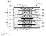
- FIG. 12 is a schematic sectional drawing of the 6th modification of the ESD protection structure which concerns on the 2nd Embodiment of this invention.
- FIG. 13 is a schematic sectional drawing of the 7th modification of the ESD protection structure which concerns on the 2nd Embodiment of this invention.
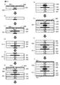
- FIG. 14 is a schematic diagram for explaining the first embodiment of the method for manufacturing an ESD protection structure according to one embodiment of the present invention.
- FIG. 15 is a schematic diagram for explaining a second embodiment of the method for manufacturing an ESD protection structure according to one embodiment of the present invention.
- FIG. 16 is a schematic diagram illustrating the procedure of Method 1 for forming an unfired heat dissipation / connection pad.
- FIG. 17 is a schematic diagram illustrating the procedure of Method 2 for forming an unfired heat dissipation / connection pad.
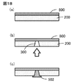
- FIG. 18 is a schematic diagram illustrating the procedure of Method 3 for forming an unfired heat dissipation / connection pad.
- FIG. 19 is a schematic diagram illustrating the procedure of Method 4 for forming an unfired heat dissipation / connection pad.
- FIG. 20 is a schematic cross-sectional view showing an example of an ESD protection structure according to an embodiment of the present invention mounted on a multilayer substrate.
- FIG. 21 is a schematic cross-sectional view of the ESD protection structure of Comparative Example 1.
- FIG. 1 is a schematic cross-sectional view of an ESD protection structure according to the first embodiment of the present invention.
- the longitudinal direction of the ESD protection structure 1 is the length direction (L direction)
- the direction perpendicular to the length direction in the horizontal plane is the width direction (W direction).
- the stacking direction of the ceramic layers is sometimes referred to as the thickness direction (T direction).
- the ESD protection structure 1 according to this embodiment includes a first laminated body portion 11 including one or more ceramic layers (indicated by 21, 22 and 25 in FIG.
- the electrode exposed region and the second electrode exposed region, and the first electrode exposed region disposed outside the first multilayer body part 11 via the interlayer connection conductor 3 included in the first multilayer body part 11 The first electrode 71 that conducts and the second stacked body portion 12 are arranged outside the second laminated body portion 12, and the second electrode And a second electrode 72 electrically connected to the second electrode exposed region through the interlayer connection conductors 3 contained Sotai portion 12.
- the first electrode exposed region is such that the surface of the opposing pad electrode 52 disposed on the surface of the ceramic layer 22 in contact with the cavity 6 is the inside of the cavity 6.
- the second electrode exposed region is a region where the surface of the opposed pad electrode 52 disposed on the surface of the ceramic layer 23 in contact with the cavity 6 is exposed to the inside of the cavity 6. Point to.
- the first electrode exposed region and the second electrode exposed region are also collectively referred to as “electrode exposed region”.
- the ceramic layers 21 to 25 may include a conventional ceramic material.
- the ceramic layer may include a ceramic material containing Ba, Al, and Si as main components, a low temperature sintered ceramics (LTCC) such as glass ceramics, and a magnetic ceramic.
- LTCC low temperature sintered ceramics
- the ceramic layers included in the first multilayer body portion 11 and the second multilayer body portion 12 include one or more interlayer connection conductors 3.
- the ceramic layers 21 to 25 each include one interlayer connection conductor 3.
- the interlayer connection conductor 3 included in each ceramic layer is directly or directly added to the interlayer connection conductor 3 included in the adjacent ceramic layer or a heat dissipation / connection pad. Electrical connection via heat dissipation / connection pads.
- the part pad electrode 52 can be regarded as constituting a pair of discharge electrodes in the ESD protection structure 1.
- the interlayer connection conductor 3, the heat dissipation / connection pad 51, and the counter part pad electrode 52 included in the first multilayer body portion 11 are electrically connected to the first electrode exposed region, and the interlayer connection conductor included in the second multilayer body portion 12. 3.
- the heat radiation / connection pad 51 and the counter part pad electrode 52 are electrically connected to the second electrode exposed region.
- the electrode exposure region (first electrode exposure region) of one discharge electrode (interlayer connection conductor 3, heat dissipation / connection pad 51, and counter part pad electrode 52) and the other
- the electrode exposed regions (second electrode exposed regions) of the discharge electrodes are arranged to face each other in the cavity 6. it can.
- the discharge electrode formed by the interlayer connection conductor 3 from the external electrode (the first electrode 71 and the second electrode 72 in the embodiment shown in FIG. 1) to the cavity 6 where electrostatic discharge occurs is as follows.
- the ESD protection structure according to the present embodiment can be suitably used in applications that need to cope with a large current.
- the discharge electrode formed by the interlayer connection conductor 3 from the external electrode to the cavity 6 is more resistant to repeated electrostatic discharges than the discharge electrode formed by conventional printing. It also has the advantage of. Heat is generated when electrostatic discharge occurs at the opposing portion of the discharge electrode. With a conventional printed discharge electrode, the electrode may be peeled off or deteriorated due to heat generation, and the resistance of the discharge electrode may be deteriorated.
- the discharge electrode composed of the interlayer connection conductor is structurally unlikely to peel off, and since the volume of the metal component is larger than that of the conventional discharge electrode, the temperature rise due to heat generation is unlikely to occur. Electrode peeling is unlikely to occur.
- the discharge electrode constituted by the interlayer connection conductor 3 has a higher resistance to heat than a discharge electrode formed by conventional printing, and thus exhibits excellent resistance when repeated electrostatic discharges. .
- the ESD protection structure according to the present embodiment can be suitably used in applications that need to cope with a large current.
- the hollow portion 6 is disposed between the first laminate portion 11 and the second laminate portion 12.
- the dimension and shape of the hollow portion 6 are not particularly limited, and for example, a shape such as a columnar shape as well as a rectangle as shown in FIG. 1 can be appropriately selected.
- the distance between the first electrode exposed region and the second electrode exposed region is the thickness (T Direction dimension).
- the thickness of the cavity 6 is controlled by the coating thickness of the cavity forming paste as will be described later.
- the coating thickness of the cavity forming paste is determined by a conventional method for setting the distance between discharge electrodes by controlling the printing position (for example, Patent Document 1). It is possible to control more accurately compared to the above method. Therefore, in the ESD protection structure 1 of the present embodiment, it is possible to control the thickness of the cavity 6 with high accuracy even when the design thickness of the cavity 6 is small.
- the size of the protective structure 1 can be reduced.
- the cavity 6 is arranged such that the entire electrode exposed region (first electrode exposed region and second electrode exposed region) exists inside the cavity 6 in plan view. By disposing the cavity portion 6 in this way, the first electrode exposed region and the second electrode exposed region can be disposed to face each other in the cavity portion 6.
- a plane is formed between the ceramic layer in which the electrode exposure region is disposed and the ceramic layer adjacent to the ceramic layer.
- a heat dissipating / connecting pad having an area larger than the area of the electrode exposure region in view is disposed.
- the heat radiation / connection pad 51 is arranged in both the first laminated body portion 11 and the second laminated body portion 12.
- the heat dissipation / connection pad 51 is arranged between the ceramic layer 22 in which the electrode exposed region is arranged and the ceramic layer 21 adjacent to the ceramic layer, and the second laminated body portion 12.
- the heat radiation / connection pad 51 is disposed between the ceramic layer 23 in which the electrode exposure region is disposed and the ceramic layer 24 adjacent to the ceramic layer.
- the heat dissipation / connection pad 51 includes an interlayer connection conductor 3 included in a ceramic layer (indicated by 22 in FIG. 1) in which the first electrode exposed region is disposed, and an electrode exposed region. It arrange
- the heat dissipation / connection pad 51 includes the interlayer connection conductor 3 included in the ceramic layer (indicated by 23 in FIG. 1) in which the first electrode exposure region is disposed, and the electrode exposure. It arrange
- positioned may be connected.
- the heat dissipation / connection pad 51 has an area larger than the area of the electrode exposure region in plan view.
- the electrode exposure region is a region where the surface of the counter part pad electrode 52 is exposed inside the cavity 6, and the area of the electrode exposure region is the counter part pad electrode 52 in plan view. It is represented by the area. Therefore, in the present embodiment, the heat dissipation / connection pad 51 has an area larger than the area of the opposed pad electrode 52 in plan view.
- the large-area heat radiation / connection pad 51 is disposed directly below and / or directly above the opposing portion of the discharge electrode (the opposing portion of the first electrode exposed region and the second electrode exposed region in the cavity 6). Thereby, the tolerance when the ESD protection structure 1 repeats electrostatic discharge can be improved.
- the mechanism by which the resistance to repeated electrostatic discharge is improved by the arrangement of the heat dissipation / connection pad 51 is not restricted by any theory, but is considered to be as follows.
- electrostatic discharge occurs in the ESD protection structure 1
- heat is generated at the facing portion of the discharge electrode.
- Deterioration of the discharge electrode occurs due to the generated heat, and the distance between the opposing discharge electrodes can change.
- the discharge characteristics may be deteriorated.
- a load may be applied to the joint portion between each member of the ESD protection structure 1 due to a difference in thermal expansion coefficient.
- the joint between the members of the ESD protection structure 1 may be destroyed.
- the heat radiation / connection pad 51 having a large area is disposed immediately below and / or directly above the facing portion of the discharge electrode, heat generated in the facing portion can be easily dissipated, and the heat radiation characteristics are greatly improved. As a result, the load that can be applied to the joint between the members due to the generated heat can be reduced, and the resistance when electrostatic discharge repeatedly occurs is improved.
- the shape of the heat dissipation / connection pad 51 is not particularly limited, and a shape such as a circle or a rectangle can be selected as appropriate.
- the heat dissipating / connecting pad 51 is preferably arranged so that at least a part of the cavity 6 overlaps the heat dissipating / connecting pad 51 in a plan view, and more preferably, the entire cavity 6 in the plan view is the heat dissipating / connecting pad 51. Arranged to exist inside. By disposing the heat dissipation / connection pad 51 in this manner, heat dissipation generated when electrostatic discharge occurs becomes easier, and as a result, resistance to repeated occurrence of electrostatic discharge can be further improved. Can do.
- the heat dissipation / connection pad 51 is preferably arranged so that at least a part of the electrode exposure region (first electrode exposure region or second electrode exposure region) overlaps the heat dissipation / connection pad 51 in plan view.
- the entire electrode exposed region is disposed inside the heat radiation / connection pad 51 in plan view.
- the heat dissipation / connection pad 51 is preferably arranged so that at least a part of the counter part pad electrode 52 overlaps the heat dissipation / connection pad 51 in plan view, and the counter part pad electrode 52 in plan view. Is more preferably disposed so as to be inside the heat radiation / connection pad 51.
- the area of the heat dissipation / connection pad 51 is desirably larger than the area of the electrode exposure region (the area of the surface of the interlayer connection conductor exposed in the cavity 6 or the area of the opposing pad electrode 52).
- the heat dissipation / connection pad 51 may cause peeling. There is. Therefore, it is desirable that the end portion of the heat dissipation / connection pad is separated from the end portion of the laminated body by 100 ⁇ m or more.
- the facing portion pad electrode is arranged on the surface of the ceramic layer in contact with the cavity 6 so as to cover the interlayer connection conductor included in the ceramic layer. May be.
- the opposing portion pad electrode 52 is disposed in both the first stacked body portion 11 and the second stacked body portion 12. In the first multilayer body portion 11, the opposing portion pad electrode 52 is disposed on the surface of the ceramic layer 22 in contact with the cavity portion 6 so as to cover the interlayer connection conductor 3 included in the ceramic layer 22.
- the facing portion pad electrode 52 is disposed on the surface of the ceramic layer 23 in contact with the cavity portion 6 so as to cover the interlayer connection conductor 3 included in the ceramic layer 23.
- the surface of the counter part pad electrode 52 is exposed to the inside of the cavity 6 to form an electrode exposed region (a first electrode exposed region and a second electrode exposed region).
- the area of the counter part pad electrode 52 constituting a part of the inner wall of the cavity 6 is increased, there is a possibility that cracks or cracks may occur in the ceramic layer.
- the area of the counter part pad electrode 52 is made smaller than the area of the heat radiation / connection pad 51 disposed immediately below and / or immediately above the discharge electrode counter part, the occurrence of the cracks and cracks described above can be suppressed. it can.
- the shape of the counter pad electrode 52 is not particularly limited, and a shape such as a circle or a rectangle can be selected as appropriate.
- the area of the counter part pad electrode 52 is preferably smaller than the area of the cavity 6 in plan view, and is preferably arranged so that the entire counter part pad electrode 52 exists inside the cavity part 6 in plan view.
- the dimension of the opposing part pad electrode 52 can be appropriately set according to the diameter and number of the interlayer connection conductors 3 included in the ceramic layer in which the opposing part pad electrode 52 is disposed.
- the diameter of the counter part pad electrode 52 is about 50 ⁇ m or more and about 200 ⁇ m or less, although it depends on the diameter of the interlayer connection conductor 3. It may be about.
- the ceramic layer on which the facing portion pad electrode 52 is arranged includes nine (3 in the L direction ⁇ 3 in the W direction) interlayer connection conductors 3, the interlayer connection conductor 3
- the diameter of the counter part pad electrode 52 may be about 150 ⁇ m or more and about 600 ⁇ m or less.
- the interlayer connection conductor is made of a material different from that of the heat dissipation / connection pad and, if present, the opposing portion pad electrode and the additional heat dissipation / connection pad. It's okay.
- the first electrode and / or the second electrode may also be made of a material different from that of the interlayer connection conductor.
- the interlayer connection conductor 3 in both the first multilayer body portion 11 and the second multilayer body portion 12, the interlayer connection conductor 3 includes the heat dissipation / connection pad 51, the opposing portion pad electrode 52, and the first electrode. 71 and the second electrode 72 are made of different materials.
- the interlayer connection conductor 3 is formed by filling a via hole formed in the ceramic layer with a conductive material.
- the interlayer connection conductor 3 includes a conductive component such as Cu, Ag, Pd, or Au.
- the interlayer connection conductor 3 may contain additives such as ceramic powder and metal oxide in addition to the above-described conductive component.
- the heat dissipation / connection pad 51, the counter pad electrode 52, the first electrode 71, and the second electrode 72 may all be made of the same material, or may be made of different materials.
- the heat dissipation / connection pad 51, the counter pad electrode 52, the first electrode 71, and the second electrode 72 preferably include the same type of conductive component as the interlayer connection conductor, such as Cu, Ag, Pd, Au, etc. It is preferable to contain.
- the shape of the interlayer connection conductor 3 is not particularly limited, and may be, for example, a substantially cylindrical shape or a substantially truncated cone shape.
- the interlayer connection conductor 3 has a substantially truncated cone shape in which one end portion is tapered.
- the interlayer connection conductor has a diameter closer to the second electrode on the side closer to the first electrode. You may have a taper shape smaller than a diameter.
- the diameter on the side close to the first electrode is smaller than the diameter on the side close to the second electrode. It may have a tapered shape.
- the interlayer connection conductor 3 included in the first multilayer body portion 11 has a tapered shape in which the diameter on the side close to the second electrode 72 is smaller than the diameter on the side close to the first electrode 71.
- the interlayer connection conductor 3 included in the second stacked body portion 12 has a tapered shape in which the diameter on the side close to the first electrode 71 is smaller than the diameter on the side close to the second electrode 72.
- the diameter of the interlayer connection conductor 3 may be 40 ⁇ m or more and 200 ⁇ m or less on the large diameter side, and may be 20 ⁇ m or more and 150 ⁇ m or less on the small diameter side. As the diameter of the interlayer connection conductor 3 is smaller, the dimensions of the cavity portion 6 in the L direction and the W direction can be reduced, and as a result, the ESD protection structure 1 can be reduced in size.
- the height (dimension in the T direction) of the interlayer connection conductor 3 can be appropriately set by adjusting the thickness of the ceramic layer.
- the height of the interlayer connection conductor 3 may be, for example, 5 ⁇ m or more and 200 ⁇ m or less.
- the first electrode 71 is disposed outside the first multilayer body portion 11 and is electrically connected to the first electrode exposed region via the interlayer connection conductor 3 included in the first multilayer body portion 11.
- the second electrode 72 is disposed outside the second multilayer body portion 12 and is electrically connected to the second electrode exposed region via the interlayer connection conductor 3 included in the second multilayer body portion 12.
- the first electrode 71 and the second electrode 72 may be collectively referred to as “electrodes”.
- the ESD protection structure 1 is an ESD protection element
- the first electrode 71 and the second electrode 72 function as external electrodes.
- FIG. 2 is a schematic cross-sectional view of a first modification of the ESD protection structure according to the first embodiment of the present invention.
- the first modified example has a configuration in which neither of the first stacked body part 11 and the second stacked body part 12 has the counter part pad electrode.
- the interlayer connection conductor 3 included in the ceramic layers (22 and 23) in contact with the cavity 6 is exposed to the inside of the cavity 6 in both the first multilayer body 11 and the second multilayer body 12.
- electrode exposure regions first electrode exposure region and second electrode exposure region
- the modification shown in FIG. 2 does not have a counter part pad electrode in both the 1st laminated body part 11 and the 2nd laminated body part 12
- the 1st laminated body part 11 and the 2nd laminated body part Any one of 12 may have a configuration that does not have a counter part pad electrode.
- FIG. 2 when the surface of the plurality of interlayer connection conductors 3 included in the ceramic layer 22 in contact with the cavity 6 is exposed to the inside of the cavity 6 in the first multilayer body 11, The area of the first electrode exposed region is represented by the sum of the exposed surfaces of the plurality of interlayer connection conductors 3.
- the second electrode exposed region Is represented by the total of the exposed surfaces of the plurality of interlayer connection conductors 3.
- the ceramic layers 22 and 23 in contact with the cavity 6 include a plurality of interlayer connection conductors 3.
- the ceramic layers 22 and 23 each include nine interlayer connection conductors 3 (3 in the L direction ⁇ 3 in the W direction).
- FIG. 3 shows a schematic cross-sectional view of a second modification of the ESD protection structure according to the first embodiment of the present invention.
- the interlayer connection conductor 3 included in the first multilayer body portion 11 and the interlayer connection conductor 3 included in the second multilayer body portion 12 are both the second electrode.
- the diameter close to 72 has a tapered shape smaller than the diameter close to the first electrode 71.
- a step of inverting the first unfired laminated body portion is not necessary in the manufacturing process described later. The shift can be prevented, and as a result, it is possible to more reliably secure the facing between the first electrode exposed region and the second electrode exposed region.
- FIG. 4 is a schematic cross-sectional view of a third modification of the ESD protection structure according to the first embodiment of the present invention.
- both the first laminate part 11 and the second laminate part 12 may further include one or more additional heat dissipation / connection pads 53 disposed between adjacent ceramic layers.
- additional heat radiation / connection pads 53 are arranged between the ceramic layers 21 and 25 adjacent to each other and between the ceramic layers 24 and 25, respectively.
- both the first laminated body portion 11 and the second laminated body portion 12 include the additional heat dissipation / connection pad 53, but the present invention is not limited to this configuration, Only one of the one stacked body portion 11 and the second stacked body portion 12 may include the additional heat dissipation / connection pad 53.
- the additional heat dissipation / connection pad 53 includes the interlayer connection conductor 3 included in one ceramic layer (21 and 24) in contact with the additional heat dissipation / connection pad 53 and the other ceramic layer (in contact with the additional heat dissipation / connection pad 53). 25) are arranged so as to be connected to the interlayer connection conductor 3 included in 25).
- the dimensions of the additional heat radiation / connection pad 53 are not particularly limited, and may have a larger area than the heat radiation / connection pad 51 and the opposed pad electrode 52 in a plan view, or the heat radiation / connection in a plan view.
- the counter part pad electrode, the heat dissipation / connection pad, and the additional heat dissipation / connection pad may be collectively referred to as a “pad”.
- the ceramic layers 21 to 25 each include nine interlayer connection conductors 3 (3 in the L direction ⁇ 3 in the W direction).
- FIG. 5 is a schematic cross-sectional view of a fourth modification of the ESD protection structure according to the first embodiment of the present invention.
- the counter part pad electrode 52 is disposed only on the surface of the ceramic layer 23 included in the second stacked body part 12, and the surface of the counter part pad electrode 52 is a hollow part. 6 is exposed to form a second electrode exposed region.
- the opposing portion pad electrode 52 is not disposed on the surface of the ceramic layer 22 included in the first multilayer body portion 11, and the surface on the small diameter side of the interlayer connection conductor 3 included in the ceramic layer 22 is exposed in the cavity portion. Forming a first electrode exposure region.
- FIG. 6 shows a schematic cross-sectional view of an ESD protection structure according to the second embodiment of the present invention.
- the facing portion pad electrode 52 is disposed on the surface of the ceramic layer 22 included in the first stacked body portion 11, and the surface of the facing portion pad electrode 52 is exposed inside the cavity portion 6. A first electrode exposed region is formed.
- the counter part pad electrode 52 is disposed on the surface of the ceramic layer 23 included in the second stacked body part 12, and the surface of the counter part pad electrode 52 is exposed to the inside of the cavity 6 to expose the second electrode. Form a region.
- the interlayer connection conductor 3 includes a heat dissipation / connection pad 51 and, if present, a counter portion pad electrode 52 and The additional heat dissipation / connection pad 53 may be made of the same material.
- the first electrode 71 and / or the second electrode 72 may also be made of the same material as that of the interlayer connection conductor 3. In both the first laminate portion 11 and the second laminate portion 12 shown in FIG.
- the interlayer connection conductor 3 is the same as the heat dissipation / connection pad 51, the opposing portion pad electrode 52, and the additional heat dissipation / connection pad 53. Consists of materials. In this case, since the interlayer connection conductor 3, the heat dissipation / connection pad 51, the opposed pad electrode 52, and the additional heat dissipation / connection pad 53 can be integrally formed, the interlayer connection conductor 3, the heat dissipation / connection pad 51, It is possible to prevent misalignment that may occur between the counter part pad electrode 52 and the additional heat dissipation / connection pad 53.
- the interlayer connection conductor and the heat dissipation / Position misalignment with the connection pad may occur. If the diameter of the interlayer connection conductor is reduced, this problem of misalignment tends to occur.
- integrally forming the interlayer connection conductor and the heat dissipation / connection pad using the same material in the same process it is possible to prevent positional displacement between the interlayer connection conductor and the heat dissipation / connection pad.
- the counter part pad electrode, the additional heat radiation / connection pad, and the first and second electrodes can be prevented from being displaced by being integrally formed with the interlayer connection conductor. This is advantageous even when the ESD protection structure is downsized. Further, by integrally forming the interlayer connection conductor and the heat dissipation / connection pad, it is possible to prevent the heat dissipation / connection pad from peeling off. Further, by integrally forming the interlayer connection conductor and the heat dissipation / connection pad, the man-hours in the manufacturing process can be reduced, and the material cost can be reduced. As shown in FIG.
- the interlayer connection conductor 3 included in the first multilayer body portion 11 and the second multilayer body portion 12 may have a taper shape, and the interlayer connection included in the first multilayer body portion 11.
- the direction from the large-diameter side of the conductor 3 toward the small-diameter side may be different from the direction from the large-diameter side of the interlayer connection conductor 3 included in the second multilayer body 12 toward the small-diameter side.
- the direction from the large diameter side to the small diameter side of the interlayer connection conductor 3 included in the first multilayer body portion 11 is the direction from the second electrode 72 to the first electrode 71.
- the direction from the large diameter side to the small diameter side of the interlayer connection conductor 3 included in the second multilayer body portion 12 is the same as the direction from the first electrode 71 to the second electrode 72. is there.
- FIG. 7 shows a schematic cross-sectional view of a first modification of the ESD protection structure according to the second embodiment of the present invention.
- each ceramic layer may include a plurality of interlayer connection conductors.
- each of the ceramic layers 21 to 25 includes nine interlayer connection conductors 3 (3 in the L direction ⁇ 3 in the W direction).
- FIG. 8 is a schematic cross-sectional view of a second modification of the ESD protection structure according to the second embodiment of the present invention.
- the interlayer connection conductor 3 included in the ceramic layer 23 of the second multilayer body 12 is exposed to the inside of the cavity 6 to form a second electrode exposed region.
- a counter part pad electrode 52 is disposed on the surface of the ceramic layer 22 included in the first stacked body part 11, and the surface of the counter part pad electrode 52 is exposed to the inside of the cavity 6 to expose the first electrode. Form a region.
- FIG. 8 is a schematic cross-sectional view of a second modification of the ESD protection structure according to the second embodiment of the present invention.
- the interlayer connection conductor 3 included in the ceramic layer 23 of the second multilayer body 12 is exposed to the inside of the cavity 6 to form a second electrode exposed region.
- a counter part pad electrode 52 is disposed on the surface of the ceramic layer 22 included in the first stacked body part 11, and the surface of the counter part pad electrode 52 is exposed to the inside of the cavity
- the interlayer connection conductor 3 includes the heat dissipation / connection pad 51, the counter pad electrode 52, and the additional heat dissipation / connection in both the first multilayer body portion 11 and the second multilayer body portion 12.
- the pad 53 is made of the same material.
- both the interlayer connection conductor 3 included in the first multilayer body portion 11 and the interlayer connection conductor 3 included in the second multilayer body portion 12 are close to the first electrode 71.
- the diameter of the side has a tapered shape smaller than the diameter of the side close to the second electrode 72.
- the ESD protection structure 1 has such a configuration, a step of inverting the first unfired laminated body portion is not necessary in the manufacturing process described later, and thus misalignment that may occur due to the inverting process is prevented. can do.
- FIG. 9 is a schematic cross-sectional view of a third modification of the ESD protection structure according to the second embodiment of the present invention.
- the counter part pad electrode 52 is disposed only on the surface of the ceramic layer 22 included in the first stacked body part 11, and the surface of the counter part pad electrode 52 is exposed inside the cavity 6. Forming a first electrode exposure region.
- both the interlayer connection conductor 3 included in the first multilayer body portion 11 and the interlayer connection conductor 3 included in both the second multilayer body portion 12 are connected to the second electrode 72.
- the diameter close to the first electrode 71 is smaller than the diameter close to the first electrode 71.
- the ceramic layers 21 to 25 each include nine interlayer connection conductors 3 (3 in the L direction ⁇ 3 in the W direction).
- FIG. 10 shows a schematic cross-sectional view of a fourth modification of the ESD protection structure according to the second embodiment of the present invention.
- the surface on the small diameter side of the interlayer connection conductor 3 included in the ceramic layer 22 included in the first multilayer body portion 11 is exposed to the inside of the cavity portion 6 so that the first electrode exposed region is formed.
- the surface on the small diameter side of the interlayer connection conductor 3 included in the ceramic layer 23 included in the second multilayer body portion 12 is exposed inside the cavity portion 6 to form a second electrode exposed region.
- FIG. 11 is a schematic cross-sectional view of a fifth modification of the ESD protection structure according to the second embodiment of the present invention.
- the interlayer connection conductor 3 included in the ceramic layer 22 of the first multilayer body portion 11 is exposed to the inside of the cavity portion 6 to form a first electrode exposed region
- the second laminated layer The interlayer connection conductor 3 included in the ceramic layer 23 of the body portion 12 is exposed to the inside of the cavity portion 6 to form a second electrode exposed region.
- FIG. 11 is a schematic cross-sectional view of a fifth modification of the ESD protection structure according to the second embodiment of the present invention.
- the interlayer connection conductor 3 included in the ceramic layer 22 of the first multilayer body portion 11 is exposed to the inside of the cavity portion 6 to form a first electrode exposed region
- the second laminated layer The interlayer connection conductor 3 included in the ceramic layer 23 of the body portion 12 is exposed to the inside of the cavity portion 6 to form a second electrode exposed region.
- the interlayer connection conductor 3 includes a heat dissipation / connection pad 51, and, if present, a counter portion pad electrode 52 and The additional heat dissipation / connection pad 53 may be made of the same material.
- the interlayer connection conductor 3 is present as well as the heat dissipation / connection pad 51.
- the counter pad electrode 52 and the additional heat dissipation / connection pad 53 may be made of a different material.
- the first electrode 71 and / or the second electrode 72 may also be made of the same material as the interlayer connection conductor 3 or may be made of a different material.
- the interlayer connection conductor 3 included in the first multilayer body portion 11 is made of a material different from the heat dissipation / connection pad 51 and the additional heat dissipation / connection pad 53, and the second multilayer body portion. 12 includes the same material as the heat dissipation / connection pad 51 and the additional heat dissipation / connection pad 53.
- the interlayer connection conductor 3 included in the first multilayer body portion 11 and the second multilayer body portion 12 may have a taper shape, and the interlayer connection included in the first multilayer body portion 11.
- the direction from the large-diameter side of the conductor 3 toward the small-diameter side may be different from the direction from the large-diameter side of the interlayer connection conductor 3 included in the second multilayer body 12 toward the small-diameter side.
- the direction from the large diameter side to the small diameter side of the interlayer connection conductor 3 included in the first multilayer body portion 11 is the direction from the first electrode 71 to the second electrode 72.
- the direction from the large diameter side to the small diameter side of the interlayer connection conductor 3 included in the second multilayer body portion 12 is the same as the direction from the second electrode 72 to the first electrode 71. is there.
- the ESD protection structure 1 has such a configuration, a step of inverting the first unfired laminated body portion is not necessary in the manufacturing process described later, and thus misalignment that may occur due to the inverting process is prevented. can do.
- FIG. 12 is a schematic cross-sectional view of a sixth modification of the ESD protection structure according to the second embodiment of the present invention.
- each ceramic layer may include a plurality of interlayer connection conductors.
- each of the ceramic layers 21 to 25 includes nine interlayer connection conductors 3 (3 in the L direction ⁇ 3 in the W direction).
- the counter part pad electrode 52 may be arranged in at least one of the first stacked body part 11 and the second stacked body part 12. In the modification shown in FIG. 12, the counter pad electrode 52 is disposed only on the surface of the ceramic layer 22 included in the first multilayer body 11.
- FIG. 13 is a schematic cross-sectional view of a seventh modification of the ESD protection structure according to the second embodiment of the present invention.
- the opposing portion pad electrode 52 is not disposed on both surfaces of the ceramic layer 22 included in the first stacked body portion 11 and the ceramic layer 23 included in the second stacked body portion 12. Good.
- each of the ceramic layers 21 to 25 includes nine interlayer connection conductors 3 (3 in the L direction ⁇ 3 in the W direction).
- the manufacturing method of the ESD protection structure according to the first embodiment includes a step of forming the first unfired laminated body portion 101, a step of inverting the upper and lower sides of the first unfired laminated body portion 101, and A step of laminating the cavity portion forming paste 600 and the second unfired laminated body portion 102 on the inverted first unfired laminated body portion 101, the first unfired electrode 701 and the second unfired laminated body portion 101; Forming an unfired electrode 702 to obtain an unfired electrostatic discharge protection structure, and firing the unfired electrostatic discharge protection structure to obtain an electrostatic discharge protection structure.
- FIG. 14 schematically shows an example of a method for manufacturing the ESD protection structure 1 shown in FIG.
- the manufacturing method of the ESD protection structure which concerns on this invention is not limited to embodiment shown in FIG. 14 and FIG. 15 mentioned later, You may add a change suitably according to the structure of the target ESD protection structure.
- a first unfired laminate part including one or more ceramic green sheets including one or more via holes filled with a conductive paste is formed.
- Ceramic green sheets (indicated by 201 and 204 in FIG. 14) in contact with the cavity forming paste 600 in at least one of the first unfired laminate part 101 and the second unfired laminate part 102, Between the ceramic green sheets (shown as 202 and 205 in FIG. 14) disposed adjacent to the non-fired heat dissipation / connection pad 501, The ceramic green sheet has an area larger than the area of the via hole exposed on the surface in contact with the cavity forming paste.
- At least one of the first unfired laminated body portion 101 and the second unfired laminated body portion 102 is disposed in contact with the cavity forming paste 600 and the cavity forming paste 600 (FIG. 14 may also include an unfired counter pad electrode 502 disposed between the substrate and the substrate.
- the unfired counter part pad electrode 502 may be disposed so as to cover the entire region where the via hole is exposed on the surface of the ceramic green sheet disposed in contact with the cavity forming paste 600.
- the unsintered heat dissipation / connection pad 501 has an area larger than the area of the counter part pad electrode 502 in plan view.
- both the ceramic green sheet 201 included in the first unfired laminated body portion 101 and the ceramic green sheet 204 included in the second unfired laminated body portion 102 are unfired.
- Counter part pad electrode 502 is formed.
- the unfired pad portion 503 can be manufactured by any one of Method 1 to Method 4 described below.
- the fired heat dissipation / connection pad 501, the unfired counter part pad electrode 502, and the additional unfired pad part 503 are collectively referred to as “unfired pads”.
- the ceramic green sheet 200 is formed on the carrier film 800.
- the carrier film 800 is not particularly limited as long as it can be etched by laser light, and may be a polyester film such as polyethylene terephthalate (PET) or polyethylene naphthalate.
- PET polyethylene terephthalate
- the density of the ceramic particles tends to be high on the side close to the carrier film 800, and the density of the ceramic particles tends to be low on the far side.
- one or more via holes 300 penetrating the ceramic green sheet 200 and the carrier film 800 are formed by irradiating laser light (indicated by arrows in the figure) from the carrier film 800 side.
- the laser light irradiation conditions can be appropriately set according to the materials of the ceramic green sheet 200 and the carrier film 800.
- the via hole 300 is formed by laser light irradiation, the via hole 300 has a tapered shape in which the diameter on the incident side of the laser light is larger than the diameter on the emission side.
- the conductive paste contains a metal powder such as Cu, Ag, Pd, or Au as a conductive component.
- the conductive paste may contain additives such as ceramic powder and metal oxide in addition to the above-described conductive components.
- the paste is applied to form an unfired heat dissipation / connection pad, an unfired counter pad electrode, an additional unfired heat dissipation / connection pad, or a first unfired electrode.
- FIG. 16D shows an unfired counter part pad electrode 502 as an example. In Method 1, the unfired pad is formed so as to contact the small diameter side of the via hole 300.
- the ceramic particle density in the ceramic green sheet on the large diameter side of the via hole is larger than the ceramic particle density in the ceramic green sheet on the small diameter side of the via hole. . Further, the ceramic particle density in the ceramic green sheet on the side where the unfired pad is formed is smaller than the ceramic particle density in the ceramic green sheet on the opposite side.
- the ceramic particle density in the ceramic layer on the large diameter side of the interlayer connection conductor is smaller than the small diameter side of the interlayer connection conductor. It becomes larger than the ceramic particle density in the ceramic layer.
- Method 2 Next, the procedure of Method 2 will be described below with reference to FIG. Method 2 is different from Method 1 described above in that laser light is irradiated from the ceramic green sheet 200 side.
- the ceramic green sheet 200 is formed on the carrier film 800.
- one or more via holes 300 penetrating the ceramic green sheet 200 and the carrier film 800 are formed by irradiating laser light from the ceramic green sheet 200 side.
- one or more via holes 300 are filled with a conductive paste from the carrier film 800 side.
- a heat radiation / connection pad forming paste, an opposing pad electrode forming paste, or a first electrode forming so as to cover one or more via holes is applied to form an unfired heat dissipation / connection pad, an unfired counter pad electrode, an additional unfired heat dissipation / connection pad, or a first unfired electrode.
- the unfired pad is formed so as to contact the large diameter side of the via hole 300.
- the ceramic particle density in the ceramic green sheet on the small diameter side of the via hole becomes larger than the ceramic particle density in the ceramic green sheet on the large diameter side of the via hole. . Further, the ceramic particle density in the ceramic green sheet on the side where the unfired pad is formed is smaller than the ceramic particle density in the ceramic green sheet on the opposite side.
- the ceramic particle density in the ceramic layer on the small diameter side of the interlayer connection conductor in the finished ESD protection structure is the large diameter side of the interlayer connection conductor. It becomes larger than the ceramic particle density in the ceramic layer.
- Method 3 uses the same paste as the conductive paste and the pad forming paste, and fills the via hole 300 with the conductive paste and forms an unfired pad in one step. Different from method 2. First, as shown in FIG. 18A, the ceramic green sheet 200 is formed on the carrier film 800.
- one or more via holes 300 penetrating only the ceramic green sheet 200 are formed by irradiating laser light from the ceramic green sheet 200 side.
- the via hole 300 By forming the via hole 300 in this manner, the diameter of the via hole 300 can be reduced, and as a result, the ESD protection structure 1 can be further reduced in size.
- the via hole 300 is formed by irradiating laser light from the ceramic green sheet 200 side, it is sufficient to form a hole penetrating only the ceramic green sheet 200, and it is necessary to open a hole penetrating the carrier film 800. There is no. Therefore, it is possible to form the via hole 300 having a small diameter of, for example, 20 ⁇ m or more and 30 ⁇ m or less.
- the conductive paste when the conductive paste is applied to the surface of the ceramic green sheet 200 so as to cover the one or more via holes 300, the one or more via holes 300 are filled with the conductive paste.
- an unfired heat dissipation / connection pad, an unfired counter part pad electrode, an additional unfired heat dissipation / connection pad, or a first unfired electrode is formed.
- the unfired pad is formed so as to be in contact with the large diameter side of the via hole 300.
- the interlayer connection conductor and the pad can be formed of the same material, and the material cost can be reduced.
- the ceramic particle density in the ceramic green sheet on the small diameter side of the via hole is larger than the ceramic particle density in the ceramic green sheet on the large diameter side of the via hole.
- the ceramic particle density in the ceramic green sheet on the side where the unfired pad is formed is smaller than the ceramic particle density in the ceramic green sheet on the opposite side.
- the ceramic particle density in the ceramic layer on the small diameter side of the interlayer connection conductor in the finished ESD protection structure is the large diameter side of the interlayer connection conductor. It becomes larger than the ceramic particle density in the ceramic layer.
- Method 4 Next, the procedure of Method 4 will be described below with reference to FIG. Method 4 is different from Method 3 described above in that a via hole 300 penetrating the ceramic green sheet 200 and the carrier film 800 is formed by irradiating laser light from the carrier film 800 side. First, as shown in FIG. 19A, the ceramic green sheet 200 is formed on the carrier film 800.
- one or more via holes 300 penetrating the ceramic green sheet 200 and the carrier film 800 are formed by irradiating laser light from the carrier film 800 side.
- the conductive paste is applied to the surface of the ceramic green sheet 200 so as to cover the one or more via holes 300
- the one or more via holes 300 are filled with the conductive paste.
- an unfired heat dissipation / connection pad, an unfired counter part pad electrode, an additional unfired heat dissipation / connection pad, or a first unfired electrode is formed.
- the unfired pad is formed so as to contact the small diameter side of the via hole 300.
- the interlayer connection conductor and the pad can be formed of the same material, and the material cost can be reduced.
- the ceramic particle density in the ceramic green sheet on the large diameter side of the via hole is larger than the ceramic particle density in the ceramic green sheet on the small diameter side of the via hole.
- the ceramic particle density in the ceramic green sheet on the side where the unfired pad is formed is smaller than the ceramic particle density in the ceramic green sheet on the opposite side.
- the ceramic particle density in the ceramic layer on the large diameter side of the interlayer connection conductor is smaller than the small diameter side of the interlayer connection conductor. It becomes larger than the ceramic particle density in the ceramic layer.
- a first green laminate is obtained by laminating ceramic green sheets having via holes and pads formed by any one of the above-described methods 1 to 4 as shown in FIGS. 14 (a) to (d). Part 101 is obtained.
- the carrier film 800 is peeled after each ceramic green sheet is laminated.
- the via hole 300, the unfired heat dissipation / connection pad 501, and the unfired counter part pad electrode 502 included in the first unfired stacked body portion 101 are formed by the method 1.
- the first unfired laminated body is turned upside down.
- the cavity portion forming paste 600 and the conductive paste 1 are filled on the first unfired laminated body portion 101 that is turned upside down.
- a second unfired laminate portion 102 including one or more ceramic green sheets 204 to 206 including the via hole 300 is stacked.
- the region where the via hole is exposed on the upper surface of the first unfired laminated body portion that is turned upside down or the entire surface of the unfired counter portion pad electrode 502 is used for forming the cavity portion.
- the region where the via hole is exposed on the lower surface of the second unfired laminated body 102 or the entire surface of the unfired counter part pad electrode 502 is covered with the paste 600 to form the cavity forming paste 600. Arranged to be covered.
- a resin that decomposes and disappears upon firing can be used.
- PET, polypropylene, ethyl cellulose, acrylic resin, or the like can be used.
- the via hole 300 and the pad included in the second unfired laminated body portion 102 may be formed by any one of methods 1 to 4. In the method shown in FIG. 14, the via hole 300, the unfired heat dissipation / connection pad 501, and the unfired counter part pad electrode 502 included in the second unfired stacked body portion 102 are formed by the method 1.
- the method according to the second embodiment is different from the method according to the first embodiment in that it does not include a step of inverting the first unfired stacked body portion 101.
- FIG. 15 is a schematic diagram for explaining a second embodiment of the method for producing an ESD protection structure according to the present invention.
- the method according to the second embodiment is a step of forming the first unfired laminated body portion 101, and the first unfired electrode 701 is formed on the lower surface of the first unfired laminated body portion 101.
- a obtaining step In the second embodiment, description of matters common to the first embodiment is omitted, and only different points will be described. In particular, the same operational effects of the same configuration will not be sequentially described in the present embodiment.
- a first unfired laminated body portion 101 including one or more ceramic green sheets (201 to 204) including one or more via holes 300 filled with a conductive paste is formed.
- at least one of the first unfired laminate portion 101 and the second unfired laminate portion 102 is at least one additional unfired disposed between adjacent ceramic green sheets.
- the heat dissipation / connection pad 503 may be further included.
- the additional unsintered heat dissipation / connection pad 503 is a via hole exposed on the surface of the ceramic green sheet adjacent to the additional unsintered heat dissipation / connection pad 503 in contact with the additional unsintered heat dissipation / connection pad 503. Arranged to cover. In the method shown in FIG.
- both the first green laminate portion 101 and the second green laminate portion 102 include additional green heat dissipation / connection pads 503.
- the via hole 300 and the unfired heat dissipation / connection pad 501, the additional unfired heat dissipation / connection pad 503, and the first unfired electrode included in the first unfired laminated body portion 101. 701 is formed by Method 3 as shown in FIGS. In this way, the first unfired laminated body portion 101 having the first unfired electrode 701 disposed on the lower surface is obtained.
- a cavity portion forming paste 600 and one or more via holes filled with a conductive paste are formed on the first unfired laminated body portion 101.
- a second green body 102 including one or more ceramic green sheets (203 to 205) including 300 is laminated.
- the cavity portion forming paste 600 is formed so that the entire region where the via hole 300 is exposed on the upper surface of the first unfired laminated body portion 101 is covered with the cavity portion forming paste 600.
- the entire surface of the unfired counter part pad electrode 502 is disposed on the lower surface of the second unfired laminated body part 102 so as to be covered with the cavity forming paste 600.
- a second unfired electrode 702 is formed on the upper surface of the second unfired laminate 102 to obtain an unfired electrostatic discharge protection structure.
- an electrostatic discharge protection structure is obtained.
- the method according to the second embodiment can suppress misalignment that may occur when the first electrode exposed region and the second electrode exposed region are arranged to face each other by not including the inversion step. .
- the diameter of the interlayer connection conductor is reduced, it may be difficult to form the opposing structure of the discharge electrode in the cavity due to a positional shift that may occur when the ceramic green sheets are laminated.
- the problem of misalignment caused by the manufacturing method of the ESD protection structure 1 including the inversion step can be a problem particularly when the ESD protection structure is downsized.
- the reversal process when the reversal process is not included, it is possible to suppress misalignment when laminating the ceramic green sheets, and it is possible to eliminate problems caused by misalignment in the facing portion of the discharge electrode.
- FIG. 20 shows an example of an ESD protection structure according to an embodiment of the present invention mounted on a multilayer substrate.
- the ESD protection structure 1 according to the present invention can be incorporated as a part of a circuit formed on a laminated substrate.
- Example 1 As the ESD protection structure of Example 1, an ESD protection element having the configuration shown in FIG.
- the ESD protection structure of Example 1 forms the first unfired laminated body portion 101 using the method 1 described above, inverts the first unfired laminated body portion 101, It was produced by laminating the second unfired laminate part 102 formed using the method 1.
- Example 2 As an ESD protection structure of Example 2, an ESD protection element having the same configuration as that of FIG. 3 was produced.
- the ESD protection structure of Example 2 uses the method 1 described above to form the first unfired laminated body portion 101, and uses the method 1 on the first unfired laminated body portion 101.
- the second unfired laminated body portion 102 formed in this manner was laminated.
- the ESD protection structure of Example 2 had a configuration in which the ESD protection structure 1 shown in FIG.
- the ESD protection structure of Example 2 was manufactured without performing the inversion process.
- Example 3 As the ESD protection structure of Example 3, an ESD protection element having the configuration shown in FIG. 5 was produced.
- the ESD protection structure of Example 3 uses the method 2 described above to form the first unfired laminated body portion 101, and uses the method 1 on the first unfired laminated body portion 101.
- the second unfired laminated body portion 102 formed in this manner was laminated.
- the ESD protection structure of Example 3 was produced without performing the inversion process.
- Example 4 As the ESD protection structure of Example 4, an ESD protection element having the configuration shown in FIG. 6 was produced.
- the ESD protection structure of Example 4 forms the first unfired laminated body portion 101 using the method 3 described above, inverts the first unfired laminated body portion 101, The second unfired laminated body portion 102 formed by using the method 3 was laminated.
- Example 5 As an ESD protection structure of Example 5, an ESD protection element having the same configuration as that of FIG. 8 was produced.
- the ESD protection structure of Example 5 uses the method 3 described above to form the first unfired laminated body portion 101, and uses the method 3 on the first unfired laminated body portion 101.
- the second unfired laminated body portion 102 formed in this manner was laminated.
- the ESD protection structure of Example 5 had a configuration in which the ESD protection structure 1 shown in FIG.
- the ESD protection structure of Example 5 was produced without performing the inversion process.
- Example 6 As an ESD protection structure of Example 6, an ESD protection element having the configuration shown in FIG. 10 was produced. First, the first unfired laminated body portion 101 was formed using the method 3 described above. Separately, the second unfired laminated body portion 102 was formed by using the method 3 described above. After the second unfired laminated body portion 102 was inverted, the second unfired laminated body portion 102 was laminated on the first unfired laminated body portion 101, thereby producing the ESD protection structure of Example 6.
- Example 7 As the ESD protection structure of Example 7, an ESD protection element having the same configuration as that of FIG. 12 was produced.
- the ESD protection structure of Example 7 uses the method 3 described above to form the first unfired laminated body portion 101, and uses the method 1 on the first unfired laminated body portion 101.
- the second unfired laminated body portion 102 formed in this manner was laminated.
- the ESD protection structure of Example 7 had a configuration in which the ESD protection structure 1 shown in FIG.
- the ESD protection structure of Example 7 was produced without performing the inversion process.
- the diameter on the small diameter side of the interlayer connection conductor was set to 50 ⁇ m.
- the size of the counter part pad electrode was set to 0.6 ⁇ 0.3 mm.
- the ESD protection structure (conventional electrostatic discharge protection structure) 9 of Comparative Example 1 includes an element body 91, a cavity portion 93 disposed inside the element body 91, and a cavity portion 93 disposed inside the element body 91.
- the discharge electrodes 92 disposed opposite to each other and the external electrodes 94 disposed on both end faces of the element body 2 are included.
- the dimension of the ESD protection structure of Comparative Example 1 was 1.0 (length) ⁇ 0.5 (width) ⁇ 0.3 (thickness) mm.
- the dimensions of the discharge electrode were length 300 ⁇ m ⁇ width 100 ⁇ m ⁇ thickness 10 ⁇ m.
- one discharge electrode is 300 ⁇ m long ⁇ 100 ⁇ m wide (thickness 10 ⁇ m). Twelve interlayer connection conductors having a diameter of 50 ⁇ m can be arranged in the area occupied by the discharge electrode. From this, it can be seen that adopting the opposing structure of the interlayer connection conductor is advantageous for miniaturization of the ESD protection structure.
- Method 3 for forming a via hole penetrating only the ceramic green sheet is advantageous in reducing the diameter of the interlayer connection conductor as compared with Method 1 for forming a via hole penetrating both the ceramic green sheet and the carrier film. Further, the structure in which the small diameter side of the interlayer connection conductor is opposed to the cavity portion is advantageous for downsizing. When the method 3 is employed, the diameter of the interlayer connection conductor can be reduced, and further, the ESD protection element can be reduced in size.
- the diameter of the interlayer connection conductor forming the discharge part is set to 50 ⁇ m on the small diameter side, and the dimension of the ESD protection structure is 1.0 mm (L direction) ⁇ 0. 0.5 mm (W direction) ⁇ 0.3 mm (T direction).
- the size of the heat dissipation / connection pad was set to 0.6 mm ⁇ 0.3 mm.
- the discharge electrode was formed by printing, and the zero point was set for reducing the diameter.
- the displacement of the discharge electrode facing portion was evaluated on a 5-point scale. One point required the step of reversal and 5 points not required the step of reversal.
- ⁇ Peeling was evaluated with a maximum of 3 points.
- the number was 3 points.
- the interlayer connection conductor and the pad are formed separately using different materials, one point is provided.
- Example 5 Material costs were evaluated on a three-point scale. When the interlayer connection conductor and the pad were formed using the same material, there were three points. When the interlayer connection conductor and the pad are formed using different materials, one point is set. In Comparative Example 1, since the discharge electrode was formed using one kind of material, it was set at 3 points. The total score of each item was shown as a comprehensive evaluation. Table 1 shows that the structure of Example 5 is most advantageous.
- ESD protection structures of Examples 1 to 4 and Comparative Example 1 were evaluated for ESD characteristics according to the following procedure, and the operation rate was obtained.
- the ESD characteristics were evaluated based on the standard IEC61000-4-2 established by the International Electrotechnical Commission (IEC).
- Electrostatic discharges having an applied voltage of 2 kV, 3 kV, 4 kV, and 5 kV were sequentially applied to the ESD protection structures of the examples and comparative examples by contact discharge.
- the above-described electrostatic discharge was applied to 100 samples, the number of samples at which discharge started at each applied voltage was determined, and the ratio was used as the operation rate.
- the electrostatic discharge protection structure according to the present invention can be miniaturized and has excellent resistance to repeated electrostatic discharges. Therefore, the electrostatic discharge protection structure can be used in electronic devices that are small and require high reliability and high performance. Can do.
- Electrostatic discharge protection structure 11 1st laminated body part 12 2nd laminated body part 101 1st unbaked laminated body part 102 2nd unbaked laminated body part 21, 22, 23, 24, 25 Ceramic Layer 200, 201, 202, 203, 204, 205, 206 Ceramic green sheet 3 Interlayer connection conductor 300 Via hole 51 Heat dissipation / connection pad 52 Opposing pad electrode 53 Additional heat dissipation / connection pad 501 Unsintered heat dissipation / connection pad 502 Not Firing counter part pad electrode 503 Additional unsintered heat radiation / connection pad 6 Cavity part 600 Cavity part forming paste 71 First electrode 72 Second electrode 701 First unsintered electrode 702 Second unsintered part Electrode 800 Carrier film 9 Conventional electrostatic discharge protection structure 91 Element 92 Discharge electrode 93 Cavity 94 External electrode
Landscapes
- Engineering & Computer Science (AREA)
- Manufacturing & Machinery (AREA)
- Thermistors And Varistors (AREA)
- Elimination Of Static Electricity (AREA)
- Semiconductor Integrated Circuits (AREA)
- Fixed Capacitors And Capacitor Manufacturing Machines (AREA)
Abstract
L'invention concerne une structure de protection contre les décharges électrostatiques, comprenant : une première partie stratifiée qui comprend des couches de céramique contenant un ou plusieurs conducteurs de connexion inter-couches; une seconde partie stratifiée qui comprend des couches de céramique contenant un ou plusieurs conducteurs de connexion inter-couches; une partie de cavité creuse qui est disposée entre la première partie stratifiée et la seconde partie stratifiée; des première et seconde régions de mise en contact d'électrode qui sont disposées à l'intérieur de la partie cavité creuse, pour qu'elles se fassent face; une première électrode disposée à l'extérieur de la première partie stratifiée; et une seconde électrode qui est disposée à l'extérieur de la seconde partie stratifiée. Dans la première et/ou la seconde partie stratifiée, une pastille de connexion/dissipation de chaleur est disposée entre une couche céramique qui est dotée de la région de mise en contact d'électrode et une couche céramique qui lui est adjacente, ladite pastille de connexion/dissipation de chaleur ayant une aire supérieure à l'aire de la région de mise en contact d'électrode lorsqu'elle est vue en plan.
Priority Applications (2)
| Application Number | Priority Date | Filing Date | Title |
|---|---|---|---|
| CN201680005573.0A CN107112726B (zh) | 2015-02-10 | 2016-01-13 | 静电放电保护构造体以及其制造方法 |
| JP2016574693A JP6358346B2 (ja) | 2015-02-10 | 2016-01-13 | 静電気放電保護構造体およびその製造方法 |
Applications Claiming Priority (2)
| Application Number | Priority Date | Filing Date | Title |
|---|---|---|---|
| JP2015024454 | 2015-02-10 | ||
| JP2015-024454 | 2015-02-10 |
Publications (1)
| Publication Number | Publication Date |
|---|---|
| WO2016129317A1 true WO2016129317A1 (fr) | 2016-08-18 |
Family
ID=56614563
Family Applications (1)
| Application Number | Title | Priority Date | Filing Date |
|---|---|---|---|
| PCT/JP2016/050812 Ceased WO2016129317A1 (fr) | 2015-02-10 | 2016-01-13 | Structure de protection contre les décharges électrostatiques et son procédé de production |
Country Status (3)
| Country | Link |
|---|---|
| JP (1) | JP6358346B2 (fr) |
| CN (1) | CN107112726B (fr) |
| WO (1) | WO2016129317A1 (fr) |
Cited By (2)
| Publication number | Priority date | Publication date | Assignee | Title |
|---|---|---|---|---|
| WO2024246219A1 (fr) * | 2023-05-31 | 2024-12-05 | Analog Devices International Unlimited Company | Éclateurs à milieu d'arc modifié pour détection et protection contre les surcharges électriques |
| US12416652B2 (en) | 2018-03-26 | 2025-09-16 | Analog Devices International Unlimited Company | Wearable device with energy harvesting |
Citations (3)
| Publication number | Priority date | Publication date | Assignee | Title |
|---|---|---|---|---|
| WO2013065672A1 (fr) * | 2011-11-01 | 2013-05-10 | 株式会社 村田製作所 | Dispositif de protection contre les décharges électrostatiques |
| WO2014027553A1 (fr) * | 2012-08-13 | 2014-02-20 | 株式会社村田製作所 | Dispositif de protection esd |
| WO2014208215A1 (fr) * | 2013-06-24 | 2014-12-31 | 株式会社村田製作所 | Dispositif de protection contre les décharges électrostatiques |
Family Cites Families (1)
| Publication number | Priority date | Publication date | Assignee | Title |
|---|---|---|---|---|
| WO2009069270A1 (fr) * | 2007-11-27 | 2009-06-04 | Panasonic Corporation | Composant anti-électricité statique et procédé de fabrication du composant anti-électricité statique |
-
2016
- 2016-01-13 JP JP2016574693A patent/JP6358346B2/ja active Active
- 2016-01-13 CN CN201680005573.0A patent/CN107112726B/zh active Active
- 2016-01-13 WO PCT/JP2016/050812 patent/WO2016129317A1/fr not_active Ceased
Patent Citations (3)
| Publication number | Priority date | Publication date | Assignee | Title |
|---|---|---|---|---|
| WO2013065672A1 (fr) * | 2011-11-01 | 2013-05-10 | 株式会社 村田製作所 | Dispositif de protection contre les décharges électrostatiques |
| WO2014027553A1 (fr) * | 2012-08-13 | 2014-02-20 | 株式会社村田製作所 | Dispositif de protection esd |
| WO2014208215A1 (fr) * | 2013-06-24 | 2014-12-31 | 株式会社村田製作所 | Dispositif de protection contre les décharges électrostatiques |
Cited By (2)
| Publication number | Priority date | Publication date | Assignee | Title |
|---|---|---|---|---|
| US12416652B2 (en) | 2018-03-26 | 2025-09-16 | Analog Devices International Unlimited Company | Wearable device with energy harvesting |
| WO2024246219A1 (fr) * | 2023-05-31 | 2024-12-05 | Analog Devices International Unlimited Company | Éclateurs à milieu d'arc modifié pour détection et protection contre les surcharges électriques |
Also Published As
| Publication number | Publication date |
|---|---|
| JP6358346B2 (ja) | 2018-07-18 |
| CN107112726B (zh) | 2019-01-29 |
| CN107112726A (zh) | 2017-08-29 |
| JPWO2016129317A1 (ja) | 2017-08-31 |
Similar Documents
| Publication | Publication Date | Title |
|---|---|---|
| KR101499717B1 (ko) | 적층 세라믹 커패시터 및 적층 세라믹 커패시터 실장 기판 | |
| WO2017170535A1 (fr) | Module de circuit | |
| KR102574689B1 (ko) | 전자 부품 | |
| WO2014208215A1 (fr) | Dispositif de protection contre les décharges électrostatiques | |
| US10187970B2 (en) | Multilayer substrate | |
| JP2016149487A (ja) | 積層コンデンサ | |
| CN118922935A (zh) | 布线基板及半导体装置 | |
| JP6358346B2 (ja) | 静電気放電保護構造体およびその製造方法 | |
| JP6497127B2 (ja) | 積層コンデンサ | |
| JP2017204547A (ja) | 積層バリスタ | |
| CN113764170A (zh) | 层叠电感器部件 | |
| JP7272790B2 (ja) | 積層コイル部品 | |
| JP5867136B2 (ja) | 静電気保護部品 | |
| KR20190116131A (ko) | 적층형 커패시터 및 그 실장 기판 | |
| JP2016152300A (ja) | コンデンサモジュール | |
| US9780533B2 (en) | ESD protective device | |
| JP2008205135A (ja) | 積層セラミックコンデンサ及びコンデンサ実装回路基板 | |
| JP2006086274A (ja) | 積層バリスタ,積層バリスタの実装構造及びバリスタモジュール | |
| JP2014236134A (ja) | 多層配線基板およびこれを備えるプローブカード | |
| KR102004784B1 (ko) | 적층 세라믹 전자부품 및 그 실장기판 | |
| JP2023093287A (ja) | 積層型キャパシタ | |
| JP2008294206A (ja) | 電子部品、スクリーン印刷製版、及び、スクリーン印刷製版を用いた電子部品の製造方法 | |
| KR102078011B1 (ko) | 적층 세라믹 전자 부품 | |
| WO2014203638A1 (fr) | Dispositif de protection contre les décharges électrostatiques | |
| WO2012153655A1 (fr) | Dispositif de protection anti-esd |
Legal Events
| Date | Code | Title | Description |
|---|---|---|---|
| 121 | Ep: the epo has been informed by wipo that ep was designated in this application |
Ref document number: 16748962 Country of ref document: EP Kind code of ref document: A1 |
|
| ENP | Entry into the national phase |
Ref document number: 2016574693 Country of ref document: JP Kind code of ref document: A |
|
| NENP | Non-entry into the national phase |
Ref country code: DE |
|
| 122 | Ep: pct application non-entry in european phase |
Ref document number: 16748962 Country of ref document: EP Kind code of ref document: A1 |