WO2016143201A1 - Électrode transparente, son procédé de fabrication, et élément électroluminescent organique - Google Patents
Électrode transparente, son procédé de fabrication, et élément électroluminescent organique Download PDFInfo
- Publication number
- WO2016143201A1 WO2016143201A1 PCT/JP2015/083461 JP2015083461W WO2016143201A1 WO 2016143201 A1 WO2016143201 A1 WO 2016143201A1 JP 2015083461 W JP2015083461 W JP 2015083461W WO 2016143201 A1 WO2016143201 A1 WO 2016143201A1
- Authority
- WO
- WIPO (PCT)
- Prior art keywords
- transparent electrode
- conductive layer
- formation
- transparent
- metal
- Prior art date
- Legal status (The legal status is an assumption and is not a legal conclusion. Google has not performed a legal analysis and makes no representation as to the accuracy of the status listed.)
- Ceased
Links
Images


Classifications
-
- H—ELECTRICITY
- H05—ELECTRIC TECHNIQUES NOT OTHERWISE PROVIDED FOR
- H05B—ELECTRIC HEATING; ELECTRIC LIGHT SOURCES NOT OTHERWISE PROVIDED FOR; CIRCUIT ARRANGEMENTS FOR ELECTRIC LIGHT SOURCES, IN GENERAL
- H05B33/00—Electroluminescent light sources
- H05B33/12—Light sources with substantially two-dimensional [2D] radiating surfaces
- H05B33/26—Light sources with substantially two-dimensional [2D] radiating surfaces characterised by the composition or arrangement of the conductive material used as an electrode
- H05B33/28—Light sources with substantially two-dimensional [2D] radiating surfaces characterised by the composition or arrangement of the conductive material used as an electrode of translucent electrodes
-
- B—PERFORMING OPERATIONS; TRANSPORTING
- B32—LAYERED PRODUCTS
- B32B—LAYERED PRODUCTS, i.e. PRODUCTS BUILT-UP OF STRATA OF FLAT OR NON-FLAT, e.g. CELLULAR OR HONEYCOMB, FORM
- B32B15/00—Layered products comprising a layer of metal
- B32B15/04—Layered products comprising a layer of metal comprising metal as the main or only constituent of a layer, which is next to another layer of the same or of a different material
- B32B15/08—Layered products comprising a layer of metal comprising metal as the main or only constituent of a layer, which is next to another layer of the same or of a different material of synthetic resin
- B32B15/082—Layered products comprising a layer of metal comprising metal as the main or only constituent of a layer, which is next to another layer of the same or of a different material of synthetic resin comprising vinyl resins; comprising acrylic resins
-
- B—PERFORMING OPERATIONS; TRANSPORTING
- B32—LAYERED PRODUCTS
- B32B—LAYERED PRODUCTS, i.e. PRODUCTS BUILT-UP OF STRATA OF FLAT OR NON-FLAT, e.g. CELLULAR OR HONEYCOMB, FORM
- B32B15/00—Layered products comprising a layer of metal
- B32B15/04—Layered products comprising a layer of metal comprising metal as the main or only constituent of a layer, which is next to another layer of the same or of a different material
- B32B15/08—Layered products comprising a layer of metal comprising metal as the main or only constituent of a layer, which is next to another layer of the same or of a different material of synthetic resin
- B32B15/085—Layered products comprising a layer of metal comprising metal as the main or only constituent of a layer, which is next to another layer of the same or of a different material of synthetic resin comprising polyolefins
-
- B—PERFORMING OPERATIONS; TRANSPORTING
- B32—LAYERED PRODUCTS
- B32B—LAYERED PRODUCTS, i.e. PRODUCTS BUILT-UP OF STRATA OF FLAT OR NON-FLAT, e.g. CELLULAR OR HONEYCOMB, FORM
- B32B15/00—Layered products comprising a layer of metal
- B32B15/04—Layered products comprising a layer of metal comprising metal as the main or only constituent of a layer, which is next to another layer of the same or of a different material
- B32B15/08—Layered products comprising a layer of metal comprising metal as the main or only constituent of a layer, which is next to another layer of the same or of a different material of synthetic resin
- B32B15/088—Layered products comprising a layer of metal comprising metal as the main or only constituent of a layer, which is next to another layer of the same or of a different material of synthetic resin comprising polyamides
-
- B—PERFORMING OPERATIONS; TRANSPORTING
- B32—LAYERED PRODUCTS
- B32B—LAYERED PRODUCTS, i.e. PRODUCTS BUILT-UP OF STRATA OF FLAT OR NON-FLAT, e.g. CELLULAR OR HONEYCOMB, FORM
- B32B15/00—Layered products comprising a layer of metal
- B32B15/04—Layered products comprising a layer of metal comprising metal as the main or only constituent of a layer, which is next to another layer of the same or of a different material
- B32B15/08—Layered products comprising a layer of metal comprising metal as the main or only constituent of a layer, which is next to another layer of the same or of a different material of synthetic resin
- B32B15/09—Layered products comprising a layer of metal comprising metal as the main or only constituent of a layer, which is next to another layer of the same or of a different material of synthetic resin comprising polyesters
-
- B—PERFORMING OPERATIONS; TRANSPORTING
- B32—LAYERED PRODUCTS
- B32B—LAYERED PRODUCTS, i.e. PRODUCTS BUILT-UP OF STRATA OF FLAT OR NON-FLAT, e.g. CELLULAR OR HONEYCOMB, FORM
- B32B15/00—Layered products comprising a layer of metal
- B32B15/20—Layered products comprising a layer of metal comprising aluminium or copper
-
- B—PERFORMING OPERATIONS; TRANSPORTING
- B32—LAYERED PRODUCTS
- B32B—LAYERED PRODUCTS, i.e. PRODUCTS BUILT-UP OF STRATA OF FLAT OR NON-FLAT, e.g. CELLULAR OR HONEYCOMB, FORM
- B32B23/00—Layered products comprising a layer of cellulosic plastic substances, i.e. substances obtained by chemical modification of cellulose, e.g. cellulose ethers, cellulose esters, viscose
- B32B23/04—Layered products comprising a layer of cellulosic plastic substances, i.e. substances obtained by chemical modification of cellulose, e.g. cellulose ethers, cellulose esters, viscose comprising such cellulosic plastic substance as the main or only constituent of a layer, which is next to another layer of the same or of a different material
- B32B23/042—Layered products comprising a layer of cellulosic plastic substances, i.e. substances obtained by chemical modification of cellulose, e.g. cellulose ethers, cellulose esters, viscose comprising such cellulosic plastic substance as the main or only constituent of a layer, which is next to another layer of the same or of a different material of metal
-
- B—PERFORMING OPERATIONS; TRANSPORTING
- B32—LAYERED PRODUCTS
- B32B—LAYERED PRODUCTS, i.e. PRODUCTS BUILT-UP OF STRATA OF FLAT OR NON-FLAT, e.g. CELLULAR OR HONEYCOMB, FORM
- B32B27/00—Layered products comprising a layer of synthetic resin
- B32B27/16—Layered products comprising a layer of synthetic resin specially treated, e.g. irradiated
-
- B—PERFORMING OPERATIONS; TRANSPORTING
- B32—LAYERED PRODUCTS
- B32B—LAYERED PRODUCTS, i.e. PRODUCTS BUILT-UP OF STRATA OF FLAT OR NON-FLAT, e.g. CELLULAR OR HONEYCOMB, FORM
- B32B27/00—Layered products comprising a layer of synthetic resin
- B32B27/28—Layered products comprising a layer of synthetic resin comprising synthetic resins not wholly covered by any one of the sub-groups B32B27/30 - B32B27/42
- B32B27/281—Layered products comprising a layer of synthetic resin comprising synthetic resins not wholly covered by any one of the sub-groups B32B27/30 - B32B27/42 comprising polyimides
-
- B—PERFORMING OPERATIONS; TRANSPORTING
- B32—LAYERED PRODUCTS
- B32B—LAYERED PRODUCTS, i.e. PRODUCTS BUILT-UP OF STRATA OF FLAT OR NON-FLAT, e.g. CELLULAR OR HONEYCOMB, FORM
- B32B27/00—Layered products comprising a layer of synthetic resin
- B32B27/28—Layered products comprising a layer of synthetic resin comprising synthetic resins not wholly covered by any one of the sub-groups B32B27/30 - B32B27/42
- B32B27/285—Layered products comprising a layer of synthetic resin comprising synthetic resins not wholly covered by any one of the sub-groups B32B27/30 - B32B27/42 comprising polyethers
-
- B—PERFORMING OPERATIONS; TRANSPORTING
- B32—LAYERED PRODUCTS
- B32B—LAYERED PRODUCTS, i.e. PRODUCTS BUILT-UP OF STRATA OF FLAT OR NON-FLAT, e.g. CELLULAR OR HONEYCOMB, FORM
- B32B27/00—Layered products comprising a layer of synthetic resin
- B32B27/28—Layered products comprising a layer of synthetic resin comprising synthetic resins not wholly covered by any one of the sub-groups B32B27/30 - B32B27/42
- B32B27/286—Layered products comprising a layer of synthetic resin comprising synthetic resins not wholly covered by any one of the sub-groups B32B27/30 - B32B27/42 comprising polysulphones; polysulfides
-
- B—PERFORMING OPERATIONS; TRANSPORTING
- B32—LAYERED PRODUCTS
- B32B—LAYERED PRODUCTS, i.e. PRODUCTS BUILT-UP OF STRATA OF FLAT OR NON-FLAT, e.g. CELLULAR OR HONEYCOMB, FORM
- B32B27/00—Layered products comprising a layer of synthetic resin
- B32B27/28—Layered products comprising a layer of synthetic resin comprising synthetic resins not wholly covered by any one of the sub-groups B32B27/30 - B32B27/42
- B32B27/288—Layered products comprising a layer of synthetic resin comprising synthetic resins not wholly covered by any one of the sub-groups B32B27/30 - B32B27/42 comprising polyketones
-
- B—PERFORMING OPERATIONS; TRANSPORTING
- B32—LAYERED PRODUCTS
- B32B—LAYERED PRODUCTS, i.e. PRODUCTS BUILT-UP OF STRATA OF FLAT OR NON-FLAT, e.g. CELLULAR OR HONEYCOMB, FORM
- B32B27/00—Layered products comprising a layer of synthetic resin
- B32B27/30—Layered products comprising a layer of synthetic resin comprising vinyl (co)polymers; comprising acrylic (co)polymers
- B32B27/302—Layered products comprising a layer of synthetic resin comprising vinyl (co)polymers; comprising acrylic (co)polymers comprising aromatic vinyl (co)polymers, e.g. styrenic (co)polymers
-
- B—PERFORMING OPERATIONS; TRANSPORTING
- B32—LAYERED PRODUCTS
- B32B—LAYERED PRODUCTS, i.e. PRODUCTS BUILT-UP OF STRATA OF FLAT OR NON-FLAT, e.g. CELLULAR OR HONEYCOMB, FORM
- B32B27/00—Layered products comprising a layer of synthetic resin
- B32B27/30—Layered products comprising a layer of synthetic resin comprising vinyl (co)polymers; comprising acrylic (co)polymers
- B32B27/304—Layered products comprising a layer of synthetic resin comprising vinyl (co)polymers; comprising acrylic (co)polymers comprising vinyl halide (co)polymers, e.g. PVC, PVDC, PVF, PVDF
-
- B—PERFORMING OPERATIONS; TRANSPORTING
- B32—LAYERED PRODUCTS
- B32B—LAYERED PRODUCTS, i.e. PRODUCTS BUILT-UP OF STRATA OF FLAT OR NON-FLAT, e.g. CELLULAR OR HONEYCOMB, FORM
- B32B27/00—Layered products comprising a layer of synthetic resin
- B32B27/32—Layered products comprising a layer of synthetic resin comprising polyolefins
- B32B27/327—Layered products comprising a layer of synthetic resin comprising polyolefins comprising polyolefins obtained by a metallocene or single-site catalyst
-
- B—PERFORMING OPERATIONS; TRANSPORTING
- B32—LAYERED PRODUCTS
- B32B—LAYERED PRODUCTS, i.e. PRODUCTS BUILT-UP OF STRATA OF FLAT OR NON-FLAT, e.g. CELLULAR OR HONEYCOMB, FORM
- B32B27/00—Layered products comprising a layer of synthetic resin
- B32B27/34—Layered products comprising a layer of synthetic resin comprising polyamides
-
- B—PERFORMING OPERATIONS; TRANSPORTING
- B32—LAYERED PRODUCTS
- B32B—LAYERED PRODUCTS, i.e. PRODUCTS BUILT-UP OF STRATA OF FLAT OR NON-FLAT, e.g. CELLULAR OR HONEYCOMB, FORM
- B32B27/00—Layered products comprising a layer of synthetic resin
- B32B27/36—Layered products comprising a layer of synthetic resin comprising polyesters
- B32B27/365—Layered products comprising a layer of synthetic resin comprising polyesters comprising polycarbonates
-
- B—PERFORMING OPERATIONS; TRANSPORTING
- B32—LAYERED PRODUCTS
- B32B—LAYERED PRODUCTS, i.e. PRODUCTS BUILT-UP OF STRATA OF FLAT OR NON-FLAT, e.g. CELLULAR OR HONEYCOMB, FORM
- B32B3/00—Layered products comprising a layer with external or internal discontinuities or unevennesses, or a layer of non-planar shape; Layered products comprising a layer having particular features of form
- B32B3/02—Layered products comprising a layer with external or internal discontinuities or unevennesses, or a layer of non-planar shape; Layered products comprising a layer having particular features of form characterised by features of form at particular places, e.g. in edge regions
- B32B3/08—Layered products comprising a layer with external or internal discontinuities or unevennesses, or a layer of non-planar shape; Layered products comprising a layer having particular features of form characterised by features of form at particular places, e.g. in edge regions characterised by added members at particular parts
-
- B—PERFORMING OPERATIONS; TRANSPORTING
- B32—LAYERED PRODUCTS
- B32B—LAYERED PRODUCTS, i.e. PRODUCTS BUILT-UP OF STRATA OF FLAT OR NON-FLAT, e.g. CELLULAR OR HONEYCOMB, FORM
- B32B7/00—Layered products characterised by the relation between layers; Layered products characterised by the relative orientation of features between layers, or by the relative values of a measurable parameter between layers, i.e. products comprising layers having different physical, chemical or physicochemical properties; Layered products characterised by the interconnection of layers
- B32B7/04—Interconnection of layers
- B32B7/06—Interconnection of layers permitting easy separation
-
- B—PERFORMING OPERATIONS; TRANSPORTING
- B32—LAYERED PRODUCTS
- B32B—LAYERED PRODUCTS, i.e. PRODUCTS BUILT-UP OF STRATA OF FLAT OR NON-FLAT, e.g. CELLULAR OR HONEYCOMB, FORM
- B32B7/00—Layered products characterised by the relation between layers; Layered products characterised by the relative orientation of features between layers, or by the relative values of a measurable parameter between layers, i.e. products comprising layers having different physical, chemical or physicochemical properties; Layered products characterised by the interconnection of layers
- B32B7/04—Interconnection of layers
- B32B7/12—Interconnection of layers using interposed adhesives or interposed materials with bonding properties
-
- B—PERFORMING OPERATIONS; TRANSPORTING
- B32—LAYERED PRODUCTS
- B32B—LAYERED PRODUCTS, i.e. PRODUCTS BUILT-UP OF STRATA OF FLAT OR NON-FLAT, e.g. CELLULAR OR HONEYCOMB, FORM
- B32B9/00—Layered products comprising a layer of a particular substance not covered by groups B32B11/00 - B32B29/00
- B32B9/005—Layered products comprising a layer of a particular substance not covered by groups B32B11/00 - B32B29/00 comprising one layer of ceramic material, e.g. porcelain, ceramic tile
-
- B—PERFORMING OPERATIONS; TRANSPORTING
- B32—LAYERED PRODUCTS
- B32B—LAYERED PRODUCTS, i.e. PRODUCTS BUILT-UP OF STRATA OF FLAT OR NON-FLAT, e.g. CELLULAR OR HONEYCOMB, FORM
- B32B9/00—Layered products comprising a layer of a particular substance not covered by groups B32B11/00 - B32B29/00
- B32B9/04—Layered products comprising a layer of a particular substance not covered by groups B32B11/00 - B32B29/00 comprising such particular substance as the main or only constituent of a layer, which is next to another layer of the same or of a different material
- B32B9/041—Layered products comprising a layer of a particular substance not covered by groups B32B11/00 - B32B29/00 comprising such particular substance as the main or only constituent of a layer, which is next to another layer of the same or of a different material of metal
-
- C—CHEMISTRY; METALLURGY
- C23—COATING METALLIC MATERIAL; COATING MATERIAL WITH METALLIC MATERIAL; CHEMICAL SURFACE TREATMENT; DIFFUSION TREATMENT OF METALLIC MATERIAL; COATING BY VACUUM EVAPORATION, BY SPUTTERING, BY ION IMPLANTATION OR BY CHEMICAL VAPOUR DEPOSITION, IN GENERAL; INHIBITING CORROSION OF METALLIC MATERIAL OR INCRUSTATION IN GENERAL
- C23C—COATING METALLIC MATERIAL; COATING MATERIAL WITH METALLIC MATERIAL; SURFACE TREATMENT OF METALLIC MATERIAL BY DIFFUSION INTO THE SURFACE, BY CHEMICAL CONVERSION OR SUBSTITUTION; COATING BY VACUUM EVAPORATION, BY SPUTTERING, BY ION IMPLANTATION OR BY CHEMICAL VAPOUR DEPOSITION, IN GENERAL
- C23C18/00—Chemical coating by decomposition of either liquid compounds or solutions of the coating forming compounds, without leaving reaction products of surface material in the coating; Contact plating
- C23C18/16—Chemical coating by decomposition of either liquid compounds or solutions of the coating forming compounds, without leaving reaction products of surface material in the coating; Contact plating by reduction or substitution, e.g. electroless plating
- C23C18/31—Coating with metals
-
- H—ELECTRICITY
- H01—ELECTRIC ELEMENTS
- H01B—CABLES; CONDUCTORS; INSULATORS; SELECTION OF MATERIALS FOR THEIR CONDUCTIVE, INSULATING OR DIELECTRIC PROPERTIES
- H01B5/00—Non-insulated conductors or conductive bodies characterised by their form
- H01B5/14—Non-insulated conductors or conductive bodies characterised by their form comprising conductive layers or films on insulating-supports
-
- H—ELECTRICITY
- H05—ELECTRIC TECHNIQUES NOT OTHERWISE PROVIDED FOR
- H05K—PRINTED CIRCUITS; CASINGS OR CONSTRUCTIONAL DETAILS OF ELECTRIC APPARATUS; MANUFACTURE OF ASSEMBLAGES OF ELECTRICAL COMPONENTS
- H05K1/00—Printed circuits
- H05K1/02—Details
- H05K1/0274—Optical details, e.g. printed circuits comprising integral optical means
-
- H—ELECTRICITY
- H10—SEMICONDUCTOR DEVICES; ELECTRIC SOLID-STATE DEVICES NOT OTHERWISE PROVIDED FOR
- H10K—ORGANIC ELECTRIC SOLID-STATE DEVICES
- H10K50/00—Organic light-emitting devices
- H10K50/80—Constructional details
- H10K50/805—Electrodes
- H10K50/81—Anodes
- H10K50/816—Multilayers, e.g. transparent multilayers
-
- H—ELECTRICITY
- H10—SEMICONDUCTOR DEVICES; ELECTRIC SOLID-STATE DEVICES NOT OTHERWISE PROVIDED FOR
- H10K—ORGANIC ELECTRIC SOLID-STATE DEVICES
- H10K71/00—Manufacture or treatment specially adapted for the organic devices covered by this subclass
- H10K71/60—Forming conductive regions or layers, e.g. electrodes
- H10K71/611—Forming conductive regions or layers, e.g. electrodes using printing deposition, e.g. ink jet printing
-
- B—PERFORMING OPERATIONS; TRANSPORTING
- B32—LAYERED PRODUCTS
- B32B—LAYERED PRODUCTS, i.e. PRODUCTS BUILT-UP OF STRATA OF FLAT OR NON-FLAT, e.g. CELLULAR OR HONEYCOMB, FORM
- B32B2255/00—Coating on the layer surface
- B32B2255/10—Coating on the layer surface on synthetic resin layer or on natural or synthetic rubber layer
-
- B—PERFORMING OPERATIONS; TRANSPORTING
- B32—LAYERED PRODUCTS
- B32B—LAYERED PRODUCTS, i.e. PRODUCTS BUILT-UP OF STRATA OF FLAT OR NON-FLAT, e.g. CELLULAR OR HONEYCOMB, FORM
- B32B2255/00—Coating on the layer surface
- B32B2255/20—Inorganic coating
-
- B—PERFORMING OPERATIONS; TRANSPORTING
- B32—LAYERED PRODUCTS
- B32B—LAYERED PRODUCTS, i.e. PRODUCTS BUILT-UP OF STRATA OF FLAT OR NON-FLAT, e.g. CELLULAR OR HONEYCOMB, FORM
- B32B2255/00—Coating on the layer surface
- B32B2255/20—Inorganic coating
- B32B2255/205—Metallic coating
-
- B—PERFORMING OPERATIONS; TRANSPORTING
- B32—LAYERED PRODUCTS
- B32B—LAYERED PRODUCTS, i.e. PRODUCTS BUILT-UP OF STRATA OF FLAT OR NON-FLAT, e.g. CELLULAR OR HONEYCOMB, FORM
- B32B2255/00—Coating on the layer surface
- B32B2255/24—Organic non-macromolecular coating
-
- B—PERFORMING OPERATIONS; TRANSPORTING
- B32—LAYERED PRODUCTS
- B32B—LAYERED PRODUCTS, i.e. PRODUCTS BUILT-UP OF STRATA OF FLAT OR NON-FLAT, e.g. CELLULAR OR HONEYCOMB, FORM
- B32B2255/00—Coating on the layer surface
- B32B2255/26—Polymeric coating
-
- B—PERFORMING OPERATIONS; TRANSPORTING
- B32—LAYERED PRODUCTS
- B32B—LAYERED PRODUCTS, i.e. PRODUCTS BUILT-UP OF STRATA OF FLAT OR NON-FLAT, e.g. CELLULAR OR HONEYCOMB, FORM
- B32B2255/00—Coating on the layer surface
- B32B2255/28—Multiple coating on one surface
-
- B—PERFORMING OPERATIONS; TRANSPORTING
- B32—LAYERED PRODUCTS
- B32B—LAYERED PRODUCTS, i.e. PRODUCTS BUILT-UP OF STRATA OF FLAT OR NON-FLAT, e.g. CELLULAR OR HONEYCOMB, FORM
- B32B2307/00—Properties of the layers or laminate
- B32B2307/20—Properties of the layers or laminate having particular electrical or magnetic properties, e.g. piezoelectric
- B32B2307/202—Conductive
-
- B—PERFORMING OPERATIONS; TRANSPORTING
- B32—LAYERED PRODUCTS
- B32B—LAYERED PRODUCTS, i.e. PRODUCTS BUILT-UP OF STRATA OF FLAT OR NON-FLAT, e.g. CELLULAR OR HONEYCOMB, FORM
- B32B2307/00—Properties of the layers or laminate
- B32B2307/20—Properties of the layers or laminate having particular electrical or magnetic properties, e.g. piezoelectric
- B32B2307/204—Di-electric
-
- B—PERFORMING OPERATIONS; TRANSPORTING
- B32—LAYERED PRODUCTS
- B32B—LAYERED PRODUCTS, i.e. PRODUCTS BUILT-UP OF STRATA OF FLAT OR NON-FLAT, e.g. CELLULAR OR HONEYCOMB, FORM
- B32B2307/00—Properties of the layers or laminate
- B32B2307/40—Properties of the layers or laminate having particular optical properties
- B32B2307/412—Transparent
-
- B—PERFORMING OPERATIONS; TRANSPORTING
- B32—LAYERED PRODUCTS
- B32B—LAYERED PRODUCTS, i.e. PRODUCTS BUILT-UP OF STRATA OF FLAT OR NON-FLAT, e.g. CELLULAR OR HONEYCOMB, FORM
- B32B2307/00—Properties of the layers or laminate
- B32B2307/40—Properties of the layers or laminate having particular optical properties
- B32B2307/414—Translucent
-
- B—PERFORMING OPERATIONS; TRANSPORTING
- B32—LAYERED PRODUCTS
- B32B—LAYERED PRODUCTS, i.e. PRODUCTS BUILT-UP OF STRATA OF FLAT OR NON-FLAT, e.g. CELLULAR OR HONEYCOMB, FORM
- B32B2307/00—Properties of the layers or laminate
- B32B2307/40—Properties of the layers or laminate having particular optical properties
- B32B2307/422—Luminescent, fluorescent, phosphorescent
-
- B—PERFORMING OPERATIONS; TRANSPORTING
- B32—LAYERED PRODUCTS
- B32B—LAYERED PRODUCTS, i.e. PRODUCTS BUILT-UP OF STRATA OF FLAT OR NON-FLAT, e.g. CELLULAR OR HONEYCOMB, FORM
- B32B2307/00—Properties of the layers or laminate
- B32B2307/50—Properties of the layers or laminate having particular mechanical properties
- B32B2307/514—Oriented
- B32B2307/518—Oriented bi-axially
-
- B—PERFORMING OPERATIONS; TRANSPORTING
- B32—LAYERED PRODUCTS
- B32B—LAYERED PRODUCTS, i.e. PRODUCTS BUILT-UP OF STRATA OF FLAT OR NON-FLAT, e.g. CELLULAR OR HONEYCOMB, FORM
- B32B2307/00—Properties of the layers or laminate
- B32B2307/50—Properties of the layers or laminate having particular mechanical properties
- B32B2307/546—Flexural strength; Flexion stiffness
-
- B—PERFORMING OPERATIONS; TRANSPORTING
- B32—LAYERED PRODUCTS
- B32B—LAYERED PRODUCTS, i.e. PRODUCTS BUILT-UP OF STRATA OF FLAT OR NON-FLAT, e.g. CELLULAR OR HONEYCOMB, FORM
- B32B2307/00—Properties of the layers or laminate
- B32B2307/70—Other properties
- B32B2307/724—Permeability to gases, adsorption
- B32B2307/7242—Non-permeable
- B32B2307/7244—Oxygen barrier
-
- B—PERFORMING OPERATIONS; TRANSPORTING
- B32—LAYERED PRODUCTS
- B32B—LAYERED PRODUCTS, i.e. PRODUCTS BUILT-UP OF STRATA OF FLAT OR NON-FLAT, e.g. CELLULAR OR HONEYCOMB, FORM
- B32B2307/00—Properties of the layers or laminate
- B32B2307/70—Other properties
- B32B2307/724—Permeability to gases, adsorption
- B32B2307/7242—Non-permeable
- B32B2307/7246—Water vapor barrier
-
- B—PERFORMING OPERATIONS; TRANSPORTING
- B32—LAYERED PRODUCTS
- B32B—LAYERED PRODUCTS, i.e. PRODUCTS BUILT-UP OF STRATA OF FLAT OR NON-FLAT, e.g. CELLULAR OR HONEYCOMB, FORM
- B32B2307/00—Properties of the layers or laminate
- B32B2307/70—Other properties
- B32B2307/732—Dimensional properties
-
- B—PERFORMING OPERATIONS; TRANSPORTING
- B32—LAYERED PRODUCTS
- B32B—LAYERED PRODUCTS, i.e. PRODUCTS BUILT-UP OF STRATA OF FLAT OR NON-FLAT, e.g. CELLULAR OR HONEYCOMB, FORM
- B32B2307/00—Properties of the layers or laminate
- B32B2307/70—Other properties
- B32B2307/748—Releasability
-
- B—PERFORMING OPERATIONS; TRANSPORTING
- B32—LAYERED PRODUCTS
- B32B—LAYERED PRODUCTS, i.e. PRODUCTS BUILT-UP OF STRATA OF FLAT OR NON-FLAT, e.g. CELLULAR OR HONEYCOMB, FORM
- B32B2457/00—Electrical equipment
-
- B—PERFORMING OPERATIONS; TRANSPORTING
- B32—LAYERED PRODUCTS
- B32B—LAYERED PRODUCTS, i.e. PRODUCTS BUILT-UP OF STRATA OF FLAT OR NON-FLAT, e.g. CELLULAR OR HONEYCOMB, FORM
- B32B2457/00—Electrical equipment
- B32B2457/12—Photovoltaic modules
-
- B—PERFORMING OPERATIONS; TRANSPORTING
- B32—LAYERED PRODUCTS
- B32B—LAYERED PRODUCTS, i.e. PRODUCTS BUILT-UP OF STRATA OF FLAT OR NON-FLAT, e.g. CELLULAR OR HONEYCOMB, FORM
- B32B2457/00—Electrical equipment
- B32B2457/20—Displays, e.g. liquid crystal displays, plasma displays
- B32B2457/202—LCD, i.e. liquid crystal displays
-
- B—PERFORMING OPERATIONS; TRANSPORTING
- B32—LAYERED PRODUCTS
- B32B—LAYERED PRODUCTS, i.e. PRODUCTS BUILT-UP OF STRATA OF FLAT OR NON-FLAT, e.g. CELLULAR OR HONEYCOMB, FORM
- B32B2457/00—Electrical equipment
- B32B2457/20—Displays, e.g. liquid crystal displays, plasma displays
- B32B2457/206—Organic displays, e.g. OLED
-
- B—PERFORMING OPERATIONS; TRANSPORTING
- B32—LAYERED PRODUCTS
- B32B—LAYERED PRODUCTS, i.e. PRODUCTS BUILT-UP OF STRATA OF FLAT OR NON-FLAT, e.g. CELLULAR OR HONEYCOMB, FORM
- B32B2457/00—Electrical equipment
- B32B2457/20—Displays, e.g. liquid crystal displays, plasma displays
- B32B2457/208—Touch screens
-
- C—CHEMISTRY; METALLURGY
- C23—COATING METALLIC MATERIAL; COATING MATERIAL WITH METALLIC MATERIAL; CHEMICAL SURFACE TREATMENT; DIFFUSION TREATMENT OF METALLIC MATERIAL; COATING BY VACUUM EVAPORATION, BY SPUTTERING, BY ION IMPLANTATION OR BY CHEMICAL VAPOUR DEPOSITION, IN GENERAL; INHIBITING CORROSION OF METALLIC MATERIAL OR INCRUSTATION IN GENERAL
- C23C—COATING METALLIC MATERIAL; COATING MATERIAL WITH METALLIC MATERIAL; SURFACE TREATMENT OF METALLIC MATERIAL BY DIFFUSION INTO THE SURFACE, BY CHEMICAL CONVERSION OR SUBSTITUTION; COATING BY VACUUM EVAPORATION, BY SPUTTERING, BY ION IMPLANTATION OR BY CHEMICAL VAPOUR DEPOSITION, IN GENERAL
- C23C18/00—Chemical coating by decomposition of either liquid compounds or solutions of the coating forming compounds, without leaving reaction products of surface material in the coating; Contact plating
- C23C18/16—Chemical coating by decomposition of either liquid compounds or solutions of the coating forming compounds, without leaving reaction products of surface material in the coating; Contact plating by reduction or substitution, e.g. electroless plating
- C23C18/31—Coating with metals
- C23C18/38—Coating with copper
-
- C—CHEMISTRY; METALLURGY
- C25—ELECTROLYTIC OR ELECTROPHORETIC PROCESSES; APPARATUS THEREFOR
- C25D—PROCESSES FOR THE ELECTROLYTIC OR ELECTROPHORETIC PRODUCTION OF COATINGS; ELECTROFORMING; APPARATUS THEREFOR
- C25D3/00—Electroplating: Baths therefor
- C25D3/02—Electroplating: Baths therefor from solutions
- C25D3/12—Electroplating: Baths therefor from solutions of nickel or cobalt
-
- C—CHEMISTRY; METALLURGY
- C25—ELECTROLYTIC OR ELECTROPHORETIC PROCESSES; APPARATUS THEREFOR
- C25D—PROCESSES FOR THE ELECTROLYTIC OR ELECTROPHORETIC PRODUCTION OF COATINGS; ELECTROFORMING; APPARATUS THEREFOR
- C25D3/00—Electroplating: Baths therefor
- C25D3/02—Electroplating: Baths therefor from solutions
- C25D3/38—Electroplating: Baths therefor from solutions of copper
-
- C—CHEMISTRY; METALLURGY
- C25—ELECTROLYTIC OR ELECTROPHORETIC PROCESSES; APPARATUS THEREFOR
- C25D—PROCESSES FOR THE ELECTROLYTIC OR ELECTROPHORETIC PRODUCTION OF COATINGS; ELECTROFORMING; APPARATUS THEREFOR
- C25D3/00—Electroplating: Baths therefor
- C25D3/02—Electroplating: Baths therefor from solutions
- C25D3/46—Electroplating: Baths therefor from solutions of silver
-
- C—CHEMISTRY; METALLURGY
- C25—ELECTROLYTIC OR ELECTROPHORETIC PROCESSES; APPARATUS THEREFOR
- C25D—PROCESSES FOR THE ELECTROLYTIC OR ELECTROPHORETIC PRODUCTION OF COATINGS; ELECTROFORMING; APPARATUS THEREFOR
- C25D5/00—Electroplating characterised by the process; Pretreatment or after-treatment of workpieces
- C25D5/60—Electroplating characterised by the structure or texture of the layers
- C25D5/605—Surface topography of the layers, e.g. rough, dendritic or nodular layers
- C25D5/611—Smooth layers
-
- C—CHEMISTRY; METALLURGY
- C25—ELECTROLYTIC OR ELECTROPHORETIC PROCESSES; APPARATUS THEREFOR
- C25D—PROCESSES FOR THE ELECTROLYTIC OR ELECTROPHORETIC PRODUCTION OF COATINGS; ELECTROFORMING; APPARATUS THEREFOR
- C25D5/00—Electroplating characterised by the process; Pretreatment or after-treatment of workpieces
- C25D5/627—Electroplating characterised by the visual appearance of the layers, e.g. colour, brightness or mat appearance
-
- H—ELECTRICITY
- H05—ELECTRIC TECHNIQUES NOT OTHERWISE PROVIDED FOR
- H05K—PRINTED CIRCUITS; CASINGS OR CONSTRUCTIONAL DETAILS OF ELECTRIC APPARATUS; MANUFACTURE OF ASSEMBLAGES OF ELECTRICAL COMPONENTS
- H05K1/00—Printed circuits
- H05K1/02—Details
- H05K1/09—Use of materials for the conductive, e.g. metallic pattern
- H05K1/092—Dispersed materials, e.g. conductive pastes or inks
- H05K1/097—Inks comprising nanoparticles and specially adapted for being sintered at low temperature
-
- H—ELECTRICITY
- H05—ELECTRIC TECHNIQUES NOT OTHERWISE PROVIDED FOR
- H05K—PRINTED CIRCUITS; CASINGS OR CONSTRUCTIONAL DETAILS OF ELECTRIC APPARATUS; MANUFACTURE OF ASSEMBLAGES OF ELECTRICAL COMPONENTS
- H05K2201/00—Indexing scheme relating to printed circuits covered by H05K1/00
- H05K2201/01—Dielectrics
- H05K2201/0104—Properties and characteristics in general
- H05K2201/0108—Transparent
-
- H—ELECTRICITY
- H05—ELECTRIC TECHNIQUES NOT OTHERWISE PROVIDED FOR
- H05K—PRINTED CIRCUITS; CASINGS OR CONSTRUCTIONAL DETAILS OF ELECTRIC APPARATUS; MANUFACTURE OF ASSEMBLAGES OF ELECTRICAL COMPONENTS
- H05K2201/00—Indexing scheme relating to printed circuits covered by H05K1/00
- H05K2201/03—Conductive materials
- H05K2201/032—Materials
- H05K2201/0329—Intrinsically conductive polymer [ICP]; Semiconductive polymer
-
- H—ELECTRICITY
- H05—ELECTRIC TECHNIQUES NOT OTHERWISE PROVIDED FOR
- H05K—PRINTED CIRCUITS; CASINGS OR CONSTRUCTIONAL DETAILS OF ELECTRIC APPARATUS; MANUFACTURE OF ASSEMBLAGES OF ELECTRICAL COMPONENTS
- H05K2201/00—Indexing scheme relating to printed circuits covered by H05K1/00
- H05K2201/09—Shape and layout
- H05K2201/09209—Shape and layout details of conductors
- H05K2201/09654—Shape and layout details of conductors covering at least two types of conductors provided for in H05K2201/09218 - H05K2201/095
- H05K2201/09681—Mesh conductors, e.g. as a ground plane
-
- H—ELECTRICITY
- H05—ELECTRIC TECHNIQUES NOT OTHERWISE PROVIDED FOR
- H05K—PRINTED CIRCUITS; CASINGS OR CONSTRUCTIONAL DETAILS OF ELECTRIC APPARATUS; MANUFACTURE OF ASSEMBLAGES OF ELECTRICAL COMPONENTS
- H05K2203/00—Indexing scheme relating to apparatus or processes for manufacturing printed circuits covered by H05K3/00
- H05K2203/12—Using specific substances
- H05K2203/121—Metallo-organic compounds
-
- H—ELECTRICITY
- H05—ELECTRIC TECHNIQUES NOT OTHERWISE PROVIDED FOR
- H05K—PRINTED CIRCUITS; CASINGS OR CONSTRUCTIONAL DETAILS OF ELECTRIC APPARATUS; MANUFACTURE OF ASSEMBLAGES OF ELECTRICAL COMPONENTS
- H05K3/00—Apparatus or processes for manufacturing printed circuits
- H05K3/22—Secondary treatment of printed circuits
- H05K3/24—Reinforcing of the conductive pattern
- H05K3/245—Reinforcing conductive patterns made by printing techniques or by other techniques for applying conductive pastes, inks or powders; Reinforcing other conductive patterns by such techniques
- H05K3/246—Reinforcing conductive paste, ink or powder patterns by other methods, e.g. by plating
-
- H—ELECTRICITY
- H10—SEMICONDUCTOR DEVICES; ELECTRIC SOLID-STATE DEVICES NOT OTHERWISE PROVIDED FOR
- H10K—ORGANIC ELECTRIC SOLID-STATE DEVICES
- H10K2102/00—Constructional details relating to the organic devices covered by this subclass
-
- H—ELECTRICITY
- H10—SEMICONDUCTOR DEVICES; ELECTRIC SOLID-STATE DEVICES NOT OTHERWISE PROVIDED FOR
- H10K—ORGANIC ELECTRIC SOLID-STATE DEVICES
- H10K2102/00—Constructional details relating to the organic devices covered by this subclass
- H10K2102/10—Transparent electrodes, e.g. using graphene
- H10K2102/101—Transparent electrodes, e.g. using graphene comprising transparent conductive oxides [TCO]
Definitions
- the present invention relates to a transparent electrode, a manufacturing method thereof, and an organic electroluminescence element. More specifically, the present invention relates to a transparent electrode having a transparent conductive layer plated with a metal thin wire.
- the transparent electrode is an essential component.
- the transparent electrode is an indispensable component also in the touch panel, mobile phone, electronic paper, various solar cells, and various electroluminescence light control elements.
- Patent Document 1 discloses a method of firing a fine metal wire printed using an ink containing silver nanoparticles by infrared irradiation, which has proved effective, but exhibits low resistance and is preserved. Further improvement is required in terms of sex.
- the present invention has been made in view of the above-mentioned problems and situations, and a solution of the problem is to provide a transparent electrode having low resistance and high storage stability and a method for producing the same. Moreover, it is providing the organic EL element which comprises the said transparent electrode.
- the present inventor in the process of examining the cause of the above-mentioned problems, plated a thin metal wire disposed on the substrate, and further provided a transparent conductive layer, thereby providing low resistance and storage stability. was found to be able to provide a high transparent electrode, leading to the present invention.
- the above-mentioned problem according to the present invention is solved by the following means.
- a transparent electrode comprising a metal conductive layer on a substrate, The metal conductive layer has a fine metal wire and a plating layer covering the fine metal wire, A transparent conductive layer covering the substrate and the metal conductive layer on the surface of the substrate on the side on which the thin metal wires are formed; A transparent electrode, wherein the thin metal wire is formed using a metal nanoparticle ink or a metal complex ink.
- the manufacturing method of the transparent electrode characterized by having.
- An organic electroluminescence device comprising the transparent electrode according to any one of items 1 to 5.
- the above-mentioned means of the present invention can provide a transparent electrode having low resistance and high storage stability, and a method for producing the same. Moreover, the organic electroluminescent element which comprises the said transparent electrode can be provided.
- the expression mechanism or action mechanism of the effect of the present invention is not clear, but is presumed as follows. According to the present invention, it is possible to fill the fine space in the fine metal wire by plating the fine metal wire, and to reduce the unevenness, so that the contact area with the fine metal wire is reduced when the transparent conductive layer is formed. It is considered that deterioration such as oxidation in the metal thin wire can be suppressed.
- the schematic diagram showing the structure of the transparent electrode of this invention Schematic diagram of fine metal wires made from nanopaste containing metal nanoparticles
- Schematic diagram of fine metal wires made from nanopaste containing metal nanoparticles Schematic diagram of fine metal wires made from nanopaste containing metal nanoparticles
- Schematic diagram of fine metal wires made from nanopaste containing metal nanoparticles Schematic diagram of fine metal wires made from nanopaste containing metal nanoparticles
- Schematic diagram of fine metal wires made from nanopaste containing metal nanoparticles Schematic diagram of fine metal wires made from nanopaste containing metal nanoparticles
- Schematic explanatory diagram conceptually illustrating an example of a method of forming a parallel line pattern Schematic diagram illustrating an example of a method for forming a mesh-like
- the transparent electrode of the present invention is a transparent electrode having a metal conductive layer on a substrate, wherein the metal conductive layer has a fine metal wire and a plating layer covering the fine metal wire, and the side on which the fine metal wire is formed
- a transparent conductive layer covering the substrate and the metal conductive layer is provided on the surface of the substrate, and the metal fine wire is formed using a metal nanoparticle ink or a metal complex ink.
- the thin metal wire is formed by a printing method from the viewpoint of manifesting the effect of the present invention.
- the metal thin wire is formed by an ink jet parallel line drawing method because the metal conductive layer can be thinned.
- the transparent conductive layer contains a conductive polymer from the viewpoint of manifesting the effects of the present invention.
- the transparent conductive layer contains a metal oxide from the viewpoint of manifesting the effects of the present invention.
- the method for producing a transparent electrode for producing the transparent electrode of the present invention includes a step of forming a fine metal wire using metal nanoparticles or a metal complex ink on a substrate, a step of plating on the fine metal wire, and the plating. And a step of forming a transparent conductive layer on the surface of the substrate on the side where the fine metal wires are formed. Thereby, a transparent electrode with low resistance and high storage stability can be produced.
- the transparent electrode of the present invention can be suitably provided for an organic electroluminescence element. Thereby, an organic EL element with low resistance and high storage stability can be provided.
- the transparent electrode of the present invention is a transparent electrode having a metal conductive layer on a substrate, wherein the metal conductive layer has a fine metal wire and a plating layer covering the fine metal wire, and the side on which the fine metal wire is formed A transparent conductive layer covering the substrate and the metal conductive layer is provided on the surface of the substrate, and the metal fine wire is formed using a metal nanoparticle ink or a metal complex ink.
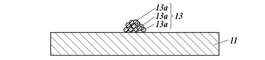
- the configuration (cross-sectional view) of the transparent electrode of the present invention is shown in FIG. As shown in FIG. 1, the transparent electrode 10 includes a metal conductive layer 12 (a thin metal wire 13 and a plating layer 14) and a transparent conductive layer 15 on a substrate 11.
- the metal conductive layer has a fine metal wire 13 and a plating layer 14 on the fine metal wire.
- substrate and the said plating layer is provided on the surface of the board
- the fine metal wires are formed using metal nanoparticle ink as shown in FIG. 2A.
- FIG. 2A one thin metal wire when the metal nanoparticle ink 13a is used is shown as an example, but the same applies when the metal complex ink is used.
- the substrate 11 is a transparent resin substrate having a total light transmittance of 80% or more in a visible light wavelength region measured by a method in accordance with JIS K 7361-1: 1997 (plastic—a method for testing the total light transmittance of a transparent material).
- plastic a method for testing the total light transmittance of a transparent material.
- transparent means that the total light transmittance in the visible light wavelength region measured by a method based on the JIS standard is 50% or more.
- the substrate 11 is preferably made of a material that is excellent in flexibility, has a sufficiently small dielectric loss coefficient, and has a microwave absorption smaller than that of the conductive layer.
- the transparent resin film that can be preferably used is not particularly limited, and the material, shape, structure, thickness and the like can be appropriately selected from known ones.
- a polyester resin film such as polyethylene terephthalate (PET), polyethylene naphthalate or modified polyester, a polyethylene (PE) resin film, a polypropylene (PP) resin film, a polyolefin resin film such as a polystyrene resin film or a cyclic olefin resin, Vinyl resin film such as polyvinyl chloride or polyvinylidene chloride, polyether ether ketone (PEEK) resin film, polysulfone (PSF) resin film, polyether sulfone (PES) resin film, polycarbonate (PC) resin film, polyamide resin Examples thereof include a film, a polyimide resin film, an acrylic resin film, and a triacetyl cellulose (TAC) resin film.
- PET polyethylene terephthalate
- PE polyethylene
- PP polyprop
- Any resin film having a total light transmittance of 80% or more can be preferably used as the substrate 11.
- a polyester resin film is preferable, and a biaxially stretched polyethylene terephthalate film and a biaxially stretched polyethylene naphthalate film are more preferable.
- substrate 11 can be surface-treated and an easily bonding layer can be provided.
- a conventionally well-known technique can be used about a surface treatment or an easily bonding layer.
- the surface treatment includes surface activation treatment such as corona discharge treatment, flame treatment, ultraviolet treatment, high frequency treatment, glow discharge treatment, active plasma treatment, and laser treatment.
- the easy adhesion layer include polyester, polyamide, polyurethane, vinyl copolymer, butadiene copolymer, acrylic copolymer, vinylidene copolymer, and epoxy copolymer.
- the easy adhesion layer may be a single layer, but may be composed of two or more layers in order to improve adhesion.
- a gas barrier layer made of an inorganic or organic film or a gas barrier layer made of an inorganic and organic hybrid film is preferably formed on the front or back surface of the substrate 11.
- the metal conductive layer 12 is a layer having a fine metal wire 13 and a plating layer 14 on the fine metal wire. It is also preferable to provide a gas barrier layer between the substrate and the metal conductive layer. The gas barrier layer will be described later.
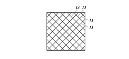
- the fine metal wires are formed in a certain fine wire pattern on the substrate.
- the metal fine wire contains metal nanoparticle ink or metal complex ink.
- the metal atom contained in the metal nanoparticle ink or the metal complex ink is not particularly limited as long as it has conductivity, for example, metals such as gold, silver, copper, iron, cobalt, nickel, chromium, and the like These alloys may be used. From the viewpoint of conductivity, silver and copper are preferable, and silver is more preferable.
- the metal nanoparticle ink is an ink containing metal nanoparticles, and may further contain a binder, a dispersant for dispersing the metal nanoparticles, and the like as necessary.
- the fine metal wire is formed in a pattern having an opening on the substrate in order to form a transparent electrode.
- the opening is a portion where a fine metal wire is not formed on the substrate and serves as a translucent window.
- the fine metal wires have a stripe pattern
- the fine metal wires have a lattice pattern
- the fine metal wires have a hexagonal honeycomb pattern, or a random mesh shape.
- a lattice-like pattern, a honeycomb-like pattern, or a random mesh-like shape is preferred, and a lattice-like pattern is most preferred from the viewpoint that even if a defect occurs in a fine metal wire, there is little influence.
- 2B to 2G show schematic diagrams of fine wire patterns of fine metal wires on the substrate.
- a method for forming a pattern of fine metal wires in a stripe shape or a lattice shape there is a method of printing in a desired shape by a relief plate, an intaglio plate, a stencil printing, an ink jet method or the like.
- the ink jet methods it is particularly preferable to print by an ink jet parallel line drawing method. Details of the ink jet parallel line drawing method will be described later.
- the aperture ratio of the metal fine wire pattern is preferably 80% or more from the viewpoint of transparency.
- An aperture ratio is the ratio which the translucent window part remove
- the aperture ratio of the stripe pattern having a line width of 100 ⁇ m and a line interval of 1 mm is approximately 90%.
- the line width of the fine metal wire is preferably 10 to 200 ⁇ m.
- the width of the thin wire is 10 ⁇ m or more, desired conductivity can be obtained, and when it is 200 ⁇ m or less, it is possible to suppress a decrease in transparency.
- the height of the fine wire is preferably 0.1 to 10 ⁇ m. When the height of the thin wire is 0.1 ⁇ m or more, desired conductivity can be obtained, and when the thickness is 10 ⁇ m or less, it is possible to suppress the occurrence of current leakage and poor layer thickness distribution in the formation of the organic electronic device.
- the average particle diameter of the metal nanoparticles is preferably in the range of 1 to 100 nm, more preferably in the range of 1 to 50 nm, and particularly preferably in the range of 1 to 30 nm.
- the average particle size of the metal nanoparticles was determined by observing 200 or more metal nanoparticles that can be observed as a circle, an ellipse, or a substantially circle or ellipse at random from an electron microscope observation of the metal nanoparticles. It is obtained by obtaining the particle size and obtaining the number average value thereof.
- the particle size refers to the minimum distance among the distances between the outer edges of the metal nanoparticles that can be observed as a circle, an ellipse, or a substantially circle or ellipse, between two parallel lines. When measuring the average particle diameter, the ones that clearly represent the side surfaces of the metal nanoparticles are not measured.
- JP 2010-265543 A, JP 2011-68936 A, JP 2012-162767 A, JP 2012-14496 A, JP 2012-14495 A, JP 2012-52225 A, Japanese Laid-Open Patent Publications Nos. 2008-214591, 2007-200755, 2006-193594, 2012-119132, 2011-153362, and JP 2009-515023 are described in detail.
- JP-T-2008-530001 also discloses a silver complex compound derived by reacting a silver compound and an ammonium carbonate compound. At the same time, an amine compound may be further contained as a reducing agent. The method for producing the metal complex ink is described in JP 2011-148759 A, JP 2008-530001 A, JP 2014-193991 A, JP 2012-92299 A, and the like.
- a method for spontaneously forming a disordered network structure of conductive fine particles by applying and drying a liquid containing metal fine particles as described in JP-T-2005-530005 can be used.
- the surface specific resistance of the substrate provided with the fine metal wires is 10 ⁇ / sq. Or less, preferably 5 ⁇ / sq. The following is preferable, and 2 ⁇ / sq. The following is more preferable.
- the surface specific resistance can be measured according to, for example, JIS K 6911-2006 or ASTM D257, and can be easily measured using a commercially available surface resistivity meter.
- a metal fine wire in the range which does not damage a film substrate.
- heating by an oven or heating by a hot plate that is generally performed can be used.
- local heat treatment may be used, and flash pulse light irradiation treatment, microwave treatment, plasma treatment, dielectric heat treatment, excimer light irradiation treatment, ultraviolet light treatment, infrared heater treatment, hot air heater treatment, and the like can be used.
- the heat treatment may be performed by using a combination of heating by an oven, heating by a hot plate, and local heat treatment.
- the metal fine wire may be provided with a base layer in order to improve pattern drawing properties and adhesion to the substrate.
- the underlayer is not particularly limited as long as it has optical transparency, and an underlayer containing organic particles such as an acrylic resin or inorganic particles such as a metal oxide is used. These include an organic or inorganic resin binder. You may use together.
- the metal oxide include various metal oxides containing a metal element selected from magnesium, aluminum, silicon, titanium, zinc, yttrium, zirconium, molybdenum, tin, barium, tantalum, and the like. Further, carbides, nitrides, borides, and the like can also be mentioned, but it is preferable that at least one transparent metal oxide is included.
- the composition of the underlayer is not particularly limited except that it is mainly composed of an inorganic compound. For example, the composition described in JP-A-2007-169604 can also be preferably used.
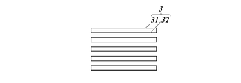
- Inkjet parallel line drawing method The ink jet parallel line drawing method will be described below with reference to FIGS.
- This phenomenon may be referred to as a coffee ring phenomenon or a coffee stain phenomenon. Since the present invention is not limited to a ring-shaped pattern, this phenomenon may be referred to as a coffee stain phenomenon in the following description.
- FIG. 3 is a schematic explanatory view for conceptually explaining an example of a method of forming a parallel line pattern using such a basic principle.
- 1 is a base material
- 2 is a line-shaped liquid containing a functional material
- 3 is formed by selectively depositing a functional material on the edge of the line-shaped liquid 2.
- It is a coating film (hereinafter also referred to as a parallel line pattern).
- H is an applying means for applying a liquid onto the substrate 1, and here is constituted by a droplet discharge device.
- the droplet discharge device H can be constituted by, for example, an inkjet head provided in an inkjet recording device.
- a liquid containing a functional material is ejected from the droplet ejection device H while the droplet ejection device H and the substrate 1 are relatively scanned, and a plurality of droplets sequentially ejected.
- the line-shaped liquid 2 containing a functional material is formed by uniting on a base material.
- FIG. 3B when the line-shaped liquid 2 is evaporated and dried, a functional material is selectively deposited on the edge of the line-shaped liquid 2 by utilizing the coffee stain phenomenon.
- the coffee stain phenomenon can be caused by setting conditions for drying the line-shaped liquid 2.
- the drying of the line-shaped liquid 2 arranged on the substrate 1 is faster at the edge than the center part, and the solid content reaches a saturated concentration as the drying proceeds, and the solid content locally reaches the edge of the line-shaped liquid 2. Precipitation occurs.
- the edge of the line-shaped liquid 2 is fixed by the deposited solid content, and shrinkage in the width direction of the line-shaped liquid 2 due to subsequent drying is suppressed. By this effect, the liquid of the line-shaped liquid 2 forms a convection from the central portion toward the edge so as to compensate for the liquid lost by evaporation at the edge.
- a parallel line pattern 3 composed of fine lines including a functional material is formed on the substrate 1.
- the parallel line pattern 3 formed from one line-shaped liquid 2 is composed of a set of two thin lines 31 and 32.
- the line segment constituting the parallel line pattern formed as described above can realize a line width of several ⁇ m
- the mesh-like functional pattern is formed by the functional material itself due to its fine line width. Even if it is not transparent, it is not recognized by the human eye and looks as if it is transparent.
- the shape of the thin line pattern of the functional material can be set by a device using the functional material.
- a touch sensor used for a touch panel uses a transparent surface electrode to detect a position by a finger or the like.
- a conductive material is used as the functional material in the mesh-shaped functional pattern, it can be preferably applied to a transparent surface electrode for a touch panel or the like. From the viewpoint of configuring a surface electrode or the like, it is very effective to increase the number of conductive paths to be meshed with a plurality of parallel line patterns having different formation directions. Examples of a method for forming such a mesh-like functional pattern include the following methods.
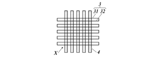
- FIG. 4 is an explanatory diagram illustrating an example (reference example) of a method for forming a mesh-like functional pattern.
- a line-shaped liquid 2 is applied on a substrate 1 in a mesh shape. That is, the line-shaped liquid 2 is applied so as to intersect at the intersection X.
- a mesh-shaped pattern with the parallel line pattern 3 can be formed.
- the line segments 31 and 32 are cut off at the intersection X where the parallel lines having different directions intersect.
- the following method may be mentioned.
- FIG. 5 is an explanatory diagram for explaining another example (reference example) of a method for forming a mesh-like functional pattern.
- the ink amount at the intersection formed by the line-shaped liquid 2 is set larger than the other parts.
- the line segments 31 and 32 at the intersection X can be prevented from being interrupted.
- the intersection X becomes a ring shape having a diameter larger than the interval between the line segments 31 and 32 as shown in FIG. 5B.
- the generation of such a ring-shaped part is advantageous in terms of preventing disconnection of the line segments 31 and 32 and facilitating, for example, ensuring conductivity, but such a ring-shaped part is periodically visible. It has been found that there is a limit in terms of further improving the low visibility.
- the following method is also exemplified as a method for preventing the line segments 31 and 32 from being cut off at the intersection X.
- FIG. 6 is an explanatory view for explaining still another example of a method for forming a mesh-like functional pattern.
- the line-shaped liquid 2 is applied in a first direction (left-right direction in the figure).
- a functional material is selectively deposited on the edge to form a first parallel line pattern 3 as shown in FIG. 6B.
- the second line is in a second direction different from the first direction (in this example, the direction is perpendicular to the first direction and is the vertical direction in the figure).
- the liquid 4 is applied. That is, the second line-shaped liquid 4 is applied so as to intersect the first parallel line pattern 3.
- a functional material is selectively deposited on the edge to form a second parallel line pattern 5 as shown in FIG. 6D.
- Reference numerals 51 and 52 denote line segments constituting the second parallel line pattern 5.
- a mesh-like functional pattern is formed by the first parallel line pattern 3 and the second parallel line pattern 5 having different formation directions. According to this method, disconnection of the line segments 31 and 32 and the line segments 51 and 52 can be prevented at the intersection X where the parallel lines having different directions intersect.
- the plated layer 14 is formed on the fine metal wire, and specifically, is formed so as to cover the fine metal wire (see FIG. 7).
- the smoothness is a value expressed by the surface roughness defined by JIS B 0601-2013, and the maximum cross-sectional height Rt (p) is preferably 500 nm or less, and preferably 200 nm or less. 100 nm or less is most preferable. The smoother the device yield, the better the continuous drivability.
- the surface roughness is a roughness related to the amplitude of fine unevenness measured using an AFM (atomic force microscope). This surface roughness can be calculated from the sectional curve of the unevenness measured continuously by measuring the inside of a section of several tens of ⁇ m many times with a detector having a stylus having a minimum tip radius of AFM.
- a method of applying plating there is a method of forming a thin metal wire on a substrate and then applying a plating agent in a desired shape by letterpress, intaglio, stencil printing or ink-jet printing and plating.
- a plating agent for example, a plating nucleus, specifically, a conductive substance dispersed in a solvent can be used.
- a conductive material used for the plating nucleus a transition metal or a compound thereof can be used. Among them, it is preferable to use an ionic transition metal, for example, it is preferable to use a transition metal such as copper, silver, gold, nickel, palladium, platinum, cobalt, and to use silver, gold, copper, etc. It is more preferable because a conductive pattern having low electric resistance and strong against corrosion can be formed.
- the conductive material it is preferable to use a particulate material having an average particle diameter of about 1 to 50 nm.
- the said average particle diameter means a center particle diameter (D50), and shows the value at the time of measuring with a laser diffraction scattering type particle size distribution measuring apparatus.
- the conductive material such as metal is preferably contained in the range of 10 to 60% by mass with respect to the total amount of the conductive ink.
- the plating agent in addition to the conductive substance, one or more kinds whose surface is coated with the metal oxide or organic substance can be used.
- the metal oxide is usually in an inactive (insulating) state, but it can be exposed to the metal and treated with a reducing agent such as dimethylaminoborane to impart activity (conductivity). It becomes.
- examples of the metal whose surface is coated with the organic substance include those in which a metal is contained in resin particles (organic substance) formed by an emulsion polymerization method or the like. These are usually in an inactive (insulating) state, but by removing the organic substance using, for example, a laser or the like, it becomes possible to expose the metal and impart activity (conductivity).
- an aqueous medium usable for the conductive ink examples include water, an organic solvent miscible with water, and a mixture thereof. It is done.
- the organic solvent miscible with water include alcohols such as methanol, ethanol, n-propanol and isopropanol; ketones such as acetone and methyl ethyl ketone; polyalkylene glycols such as ethylene glycol, diethylene glycol and propylene glycol; alkyl ethers of polyalkylene glycols And lactams such as N-methyl-2-pyrrolidone.
- water only water may be used, a mixture of water and an organic solvent miscible with water may be used, or only an organic solvent miscible with water may be used.
- water alone or a mixture of water and an organic solvent miscible with water is preferred, and water alone is particularly preferred.
- Examples of usable organic solvents include, for example, ketones such as acetone and methyl ethyl ketone; ethers such as tetrahydrofuran and dioxane; acetic esters such as ethyl acetate and butyl acetate; nitriles such as acetonitrile; dimethylformamide
- ketones such as acetone and methyl ethyl ketone
- ethers such as tetrahydrofuran and dioxane
- acetic esters such as ethyl acetate and butyl acetate
- nitriles such as acetonitrile
- An amide such as N-methylpyrrolidone can be used alone or in combination of two or more. The thing similar to what was illustrated can also be used.
- the electroless plating treatment step deposits a metal such as copper contained in the electroless plating solution by bringing the electroless plating solution into contact with the surface of a fine metal wire carrying a plating nucleus such as palladium or silver. And forming an electroless plating film made of a metal film.
- a material containing a conductive material made of a metal such as copper, nickel, chromium, cobalt, tin, a reducing agent, and a solvent such as an aqueous medium or an organic solvent may be used.
- a reducing agent that can be used include dimethylaminoborane, hypophosphorous acid, sodium hypophosphite, dimethylamine borane, hydrazine, formaldehyde, sodium borohydride, and phenols.
- monocarboxylic acids such as acetic acid and formic acid
- dicarboxylic acids such as malonic acid, succinic acid, adipic acid, maleic acid and fumaric acid
- malic acid lactic acid and glycolic acid, if necessary Hydroxycarboxylic acids such as gluconic acid and citric acid
- amino acids such as glycine, alanine, iminodiacetic acid, arginine, aspartic acid, and glutamic acid
- aminopoly acids such as iminodiacetic acid, nitrilotriacetic acid, ethylenediaminediacetic acid, ethylenediaminetetraacetic acid, and diethylenetriaminepentaacetic acid
- complexing agents such as organic acids such as carboxylic acids, soluble salts of these organic acids (sodium salts, potassium salts, ammonium salts, etc.), amines such as ethylenediamine, diethylenetriamine, and triethylenete
- the temperature of the electroless plating solution when the electroless plating solution is brought into contact with the surface of the fine metal wire carrying the plating nucleus in the plating agent is preferably in the range of about 20 to 98 ° C.
- the electrolytic plating treatment step is performed by energizing the surface of the fine metal wire carrying the plating nucleus or the surface of the electroless plating film formed by the electroless treatment with the electrolytic plating solution being in contact with the surface. Then, a metal such as copper contained in the electrolytic plating solution is deposited on the surface of the thin metal wire disposed on the negative electrode or on the surface of the electroless plating film formed by the electroless treatment, and the electrolytic plating film (metal film) Is a step of forming.
- the electroconductive substance which consists of metals, such as copper, nickel, chromium, cobalt, tin, a sulfuric acid, etc., and an aqueous medium can be used.
- the temperature of the electrolytic plating solution when the electrolytic plating solution is brought into contact with the surface of the fine metal wire carrying the plating nucleus in the plating nucleating agent is preferably in the range of about 20 to 98 ° C.
- the transparent conductive layer 15 covers the fine metal wires and the plated layer, and is formed on the substrate.
- the transparent conductive layer includes at least a conductive material (conductive material). Examples of the conductive material include a conductive transparent material and a conductive polymer.
- Conductivity in the transparent conductive layer 15 and the conductive material refers to a state in which electricity flows, and conforms to “Resistivity test method of conductive conductive plastic by four-probe method” in JIS K 7194-1994. The sheet resistance measured by the method is 10 ⁇ 7 ⁇ / sq. It means lower.
- the surface resistivity is 10,000 ⁇ / sq. In that the potential between the fine metal wires is constant. Or less, preferably 2000 ⁇ / sq. Or less, and most preferably 500 ⁇ / ⁇ or less.
- the dry layer thickness of the transparent conductive layer is preferably 30 to 2000 nm. From the viewpoint of conductivity, the thickness is more preferably 100 nm or more, and from the viewpoint of the surface smoothness of the electrode, it is further preferably 200 nm or more. Moreover, it is more preferable that it is 1000 nm or less from the point of transparency.
- a metal oxide, a conductive polymer, or the like can be used. From the viewpoint of transparency, a metal oxide is preferable. On the other hand, a conductive polymer is preferable in terms of unevenness coverage.
- the conductive transparent material is also preferably a metal oxide, such as indium tin oxide (ITO), zinc oxide (ZnO), tin oxide (SnO 2 ), conductive oxides such as IGZO, indium zinc oxide, and the like. And an amorphous transparent conductive film.
- a metal oxide such as indium tin oxide (ITO), zinc oxide (ZnO), tin oxide (SnO 2 ), conductive oxides such as IGZO, indium zinc oxide, and the like.
- an amorphous transparent conductive film is preferable, and indium zinc oxide and amorphous indium tin oxide are preferable.
- a method for producing amorphous indium tin oxide is described in JP-A-10-280127 and JP-A-2003-73860.
- the transparent conductive layer When the transparent conductive layer is formed of a conductive polymer, it preferably contains a non-conductive polymer together with the conductive polymer.
- the transparent conductive layer contains a conductive polymer and a non-conductive polymer, and the non-conductive polymer contains a self-dispersing polymer and / or a hydroxy group-containing polymer, thereby improving the conductivity of the transparent conductive layer.
- the required amount of conductive polymer can be reduced without loss. As a result, a transparent electrode having both high conductivity and transparency can be obtained.
- the conductive polymer contains a ⁇ -conjugated conductive polymer and a polyanion.
- the conductive polymer can be easily produced by chemical oxidative polymerization of a precursor monomer that forms a ⁇ -conjugated conductive polymer described later in the presence of an appropriate oxidizing agent, an oxidation catalyst, and a polyanion described later.
- the ⁇ -conjugated conductive polymer is not particularly limited, and includes polythiophenes (including basic polythiophenes, the same applies hereinafter), polypyrroles, polyindoles, polycarbazoles, polyanilines, polyacetylenes, polyfurans, polyparaffins.
- Chain conductive polymers such as phenylene vinylenes, polyazulenes, polyparaphenylenes, polyparaphenylene sulfides, polyisothianaphthenes, polythiazyls, and the like can be used.
- polythiophenes and polyanilines are preferable from the viewpoint of conductivity, transparency, stability, and the like, and polyethylenedioxythiophene is most preferable.
- Precursor monomers used for the formation of ⁇ -conjugated conductive polymers have a ⁇ -conjugated system in the molecule, and even when polymerized by the action of an appropriate oxidizing agent, a ⁇ -conjugated system is formed in the main chain.
- the Examples thereof include pyrroles and derivatives thereof, thiophenes and derivatives thereof, anilines and derivatives thereof, and the like.
- the precursor monomer examples include pyrrole, 3-methylpyrrole, 3-ethylpyrrole, 3-n-propylpyrrole, 3-butylpyrrole, 3-octylpyrrole, 3-decylpyrrole, 3-dodecylpyrrole, 3, 4-dimethylpyrrole, 3,4-dibutylpyrrole, 3-carboxylpyrrole, 3-methyl-4-carboxylpyrrole, 3-methyl-4-carboxyethylpyrrole, 3-methyl-4-carboxybutylpyrrole, 3-hydroxypyrrole 3-methoxypyrrole, 3-ethoxypyrrole, 3-butoxypyrrole, 3-hexyloxypyrrole, 3-methyl-4-hexyloxypyrrole, thiophene, 3-methylthiophene, 3-ethylthiophene, 3-propylthiophene, 3 -Butylthiophene, 3-hexyl Offene, 3-heptyl
- the polyanion used for the conductive polymer is a substituted or unsubstituted polyalkylene, a substituted or unsubstituted polyalkenylene, a substituted or unsubstituted polyimide, a substituted or unsubstituted polyamide, a substituted or unsubstituted polyester, and a combination thereof.
- This polyanion is a polymer that solubilizes or disperses a ⁇ -conjugated conductive polymer in a solvent.
- the anion group of the polyanion functions as a dopant for the ⁇ -conjugated conductive polymer, and improves the conductivity and heat resistance of the ⁇ -conjugated conductive polymer.
- the anion group of the polyanion may be a functional group capable of undergoing chemical oxidation doping to the ⁇ -conjugated conductive polymer.
- a monosubstituted sulfate group A mono-substituted phosphate group, a phosphate group, a carboxy group, a sulfo group and the like are preferable.
- a sulfo group, a monosubstituted sulfate group, and a carboxy group are more preferable.
- polyanions include polyvinyl sulfonic acid, polystyrene sulfonic acid, polyallyl sulfonic acid, polyacrylic acid ethyl sulfonic acid, polyacrylic acid butyl sulfonic acid, poly-2-acrylamido-2-methylpropane sulfonic acid, polyisoprene sulfone. Acid, polyvinyl carboxylic acid, polystyrene carboxylic acid, polyallyl carboxylic acid, polyacryl carboxylic acid, polymethacryl carboxylic acid, poly-2-acrylamido-2-methylpropane carboxylic acid, polyisoprene carboxylic acid, polyacrylic acid and the like. .
- these homopolymers may be sufficient and 2 or more types of copolymers may be sufficient.
- the polyanion which has a fluorine atom further in a compound may be sufficient.
- Nafion made by Dupont
- Flemion made by Asahi Glass Co., Ltd.
- these fluorinated polyanions can be integrally formed with a non-fluorinated polyanion to form a transparent electrode to which a hole injection function is added, which is desirable from the viewpoint of device efficiency and productivity.
- the degree of polymerization of the polyanion is preferably in the range of 10 to 100,000 monomer units, and more preferably in the range of 50 to 10,000 from the viewpoint of solvent solubility and conductivity.
- Examples of the polyanion production method include a method of directly introducing an anionic group into a polymer having no anionic group using an acid, a method of sulfonating a polymer having no anionic group with a sulfonating agent, and an anionic group-containing polymerizable monomer. The method of manufacturing by superposition
- Examples of the method for producing an anion group-containing polymerizable monomer by polymerization include a method for producing an anion group-containing polymerizable monomer in a solvent by oxidative polymerization or radical polymerization in the presence of an oxidizing agent and / or a polymerization catalyst.
- an anionic group-containing polymerizable monomer is dissolved in a solvent, this is maintained at a constant temperature, and a solution in which a predetermined amount of an oxidizing agent and / or a polymerization catalyst is dissolved in the solvent is added to the predetermined amount. React with time.
- the polymer obtained by the reaction is adjusted to a certain concentration by the solvent.
- an anionic group-containing polymerizable monomer may be copolymerized with a polymerizable monomer having no anionic group.
- the oxidizing agent, oxidation catalyst, and solvent used in the polymerization of the anionic group-containing polymerizable monomer are the same as those used in the polymerization of the precursor monomer that forms the ⁇ -conjugated conductive polymer.
- the obtained polymer is a polyanionic salt, it is preferably transformed into a polyanionic acid.
- the method for transforming into polyanionic acid include ion exchange method using ion exchange resin, dialysis method, ultrafiltration method and the like. Among these, ultrafiltration method is preferable from the viewpoint of easy work.
- the ratio of ⁇ -conjugated conductive polymer and polyanion contained in the conductive polymer, “ ⁇ -conjugated conductive polymer”: “polyanion” is preferably in the range of 1: 1 to 20 by mass ratio. From the viewpoint of conductivity and dispersibility, the range of 1: 2 to 10 is more preferable.
- oxidizing agent used for obtaining a conductive polymer by chemical oxidative polymerization of a precursor monomer that forms a ⁇ -conjugated conductive polymer in the presence of a polyanion are described in, for example, J. Org. Am. Chem. Soc. 85, 454 (1963), which is suitable for the oxidative polymerization of pyrrole.
- iron (III) salts such as iron (III) salts, FeCl 3 , Fe (ClO 4 ) 3 , iron (III) salts of inorganic acids containing organic acids and organic residues
- air and oxygen in the presence of catalytic amounts of metal ions such as iron, cobalt, nickel, molybdenum and vanadium ions can be used as oxidizing agents as needed.
- persulfates and the iron (III) salts of inorganic acids containing organic acids and organic residues has great application advantages because they are not corrosive.
- iron (III) salt of an inorganic acid containing an organic residue examples include, for example, iron (III) salt of sulfuric acid half ester of alkanol having 1 to 20 carbon atoms such as lauryl sulfuric acid, methanesulfonic acid, dodecanesulfonic acid, etc. C 1-20 alkyl sulfonic acid, 2-ethylhexyl carboxylic acid, etc., aliphatic C 1-20 carboxylic acid, trifluoroacetic acid, perfluorooctanoic acid, etc., aliphatic perfluorocarboxylic acid, oxalic acid, etc.
- Such a conductive polymer is preferably a commercially available material.
- a conductive polymer composed of poly (3,4-ethylenedioxythiophene) and polystyrenesulfonic acid (abbreviated as PEDOT / PSS) is a Clevios series from Heraeus, PEDOT-PSS 483095, 560596 from Aldrich, It is commercially available as a Denatron series from Nagase Chemtex.
- Polyaniline is commercially available from Nissan Chemical Industries as the ORMECON series.
- Non-conductive polymer examples include a self-dispersing non-conductive polymer and a hydroxy group-containing polymer.
- the self-dispersing non-conductive polymer is a polymer that is dispersible in an aqueous solvent, contains a dissociable group, and has a glass transition temperature of 25 ° C. or higher and 150 ° C. or lower.
- the self-dispersing polymer containing a dissociable group dispersible in an aqueous solvent does not contain a surfactant or an emulsifier that assists micelle formation.
- the polymer alone can be dispersed in an aqueous solvent.
- “Dispersible in an aqueous solvent” means that colloidal particles made of a binder resin are dispersed without being aggregated in the aqueous solvent.
- the use amount of the self-dispersing polymer containing a dissociable group is preferably 50 to 1000% by mass, more preferably 100 to 900% by mass, and further preferably 200 to 800% by mass with respect to the conductive polymer.
- the size of the colloidal particles is generally about 0.001 to 1 ⁇ m (1 to 1000 nm).
- the particle size is preferably 3 to 500 nm, more preferably 5 to 300 nm, and still more preferably 10 to 200 nm.
- the colloidal particles can be measured with a light scattering photometer.
- the aqueous solvent includes not only pure water (including distilled water and deionized water), but also aqueous solutions containing acids, alkalis, salts, etc., water-containing organic solvents, and hydrophilic organic solvents. .
- examples of the aqueous solvent include pure water (including distilled water and deionized water), alcohol solvents such as methanol and ethanol, and a mixed solvent of water and alcohol.
- the pH of the dispersion of the self-dispersing polymer containing a dissociable group used for the production of the transparent electrode is desirably in a range not separated from the conductive polymer solution to be separately compatible, and preferably 0.1 to 11.0. More preferably, it is 3.0 to 9.0.
- the self-dispersing polymer containing a dissociable group is preferably transparent.
- the self-dispersing polymer containing a dissociable group is not particularly limited as long as it is a medium that forms a film. Further, there is no particular limitation as long as there is no influence on the organic functional layer or the like when producing an electronic device such as a bleed-out to the transparent electrode surface or an organic EL element.
- the self-dispersing polymer dispersion does not contain a surfactant (emulsifier), a plasticizer for controlling the film forming temperature, or the like.
- the self-dispersing polymer containing a dissociable group has a glass transition temperature (Tg) of 25 ° C. or higher and 150 ° C. or lower, and preferably in the range of 30 to 110 ° C.
- Tg glass transition temperature
- the glass transition temperature is 25 ° C. or higher, the film forming property of the coating film is improved and the surface smoothness of the transparent electrode is improved. For this reason, in the environmental test of electronic devices, such as a transparent electrode and an organic EL element performed at high temperature, the deterioration of element performance by deformation
- the glass transition temperature can be determined according to JIS K 7121-1987 by using a differential scanning calorimeter (DSC-7 manufactured by Perkin Elmer Co.) at a heating rate of 10 ° C./min.
- the dissociable group used in the self-dispersing polymer containing a dissociable group is not particularly limited, and examples thereof include an anionic group (sulfonic acid and its salt, carboxylic acid and its salt, phosphoric acid and its salt, etc. ), A cationic group (such as ammonium salt) and the like. From the viewpoint of compatibility with the conductive polymer solution, an anionic group is preferable.
- the amount of the dissociable group is not particularly limited as long as the self-dispersing polymer can be dispersed in the aqueous solvent, and the drying load is reduced in an appropriate manner for the process.
- the main skeleton of the self-dispersing polymer containing a dissociable group includes polyethylene, polyethylene-polyvinyl alcohol (PVA), polyethylene-polyvinyl acetate, polyethylene-polyurethane, polybutadiene, polybutadiene-polystyrene, polyamide (nylon), and polyvinylidene chloride.
- PVA polyethylene-polyvinyl alcohol
- polyethylene-polyvinyl acetate polyethylene-polyurethane
- polybutadiene polybutadiene-polystyrene
- polyamide polyamide
- polyvinylidene chloride polyvinylidene chloride
- Polyester polyacrylate, polyacrylate-polyester, polyacrylate-polystyrene, polyvinyl acetate, polyurethane-polycarbonate, polyurethane-polyether, polyurethane-polyester, polyurethane-polyacrylate, silicone, silicone-polyurethane, silicone-polyacrylate, polyfluoride And vinylidene fluoride-polyacrylate, polyfluoroolefin-polyvinyl ether, and the like. Further, copolymers based on these skeletons and further using other monomers may be used.
- a polyester resin emulsion having an ester skeleton a polyester-acrylic resin emulsion, an acrylic resin emulsion having an acrylic skeleton, and a polyethylene resin emulsion having an ethylene skeleton are preferable.
- Yodosol AD-176, AD-137 (acrylic resin: manufactured by Henkel Japan), Vironal MD-1200, MD-1245, MD-1500 (polyester resin: manufactured by Toyobo), Plus Coat RZ570, Plus Coat Z561, Plus Coat Z565, Plus Coat Z687, Plus Coat Z690 (polyester resin: manufactured by Mutoh Chemical Co., Ltd.) and the like can be used.
- One type or a plurality of types of self-dispersing polymer dispersions containing dissociable groups that can be dispersed in the aqueous solvent can be used.
- the hydroxy group-containing polymer is a polymer having a hydroxy group.
- the ratio of the conductive polymer and the hydroxy group-containing polymer in the transparent conductive layer is preferably 30 to 900 parts by mass of the hydroxy group-containing polymer when the conductive polymer is 100 parts by mass, preventing current leakage, From the viewpoint of transparency, the hydroxy group-containing polymer is more preferably 100 parts by mass or more.
- the hydroxy group-containing polymer preferably has an absorption with an absorbance of 0.1 or more at 2.5 to 3.0 ⁇ m.
- the light absorbency here means the light absorbency of the sample at the time of apply
- the oxygen permeability measured by a method according to JIS K 7126-1987 is 1 ⁇ 10 ⁇ 3 mL / m 2 ⁇ 24 h ⁇ atm or less. It is preferable that
- a film containing an inorganic compound such as silica formed by vacuum deposition or CVD can be used.
- a film formed by applying and drying a coating solution containing a polysilazane compound and then oxidizing it with ultraviolet irradiation in a nitrogen atmosphere containing oxygen and water vapor can be used.
- a surface of the transparent resin substrate can be pretreated using a silane coupling agent or the like.
- the gas barrier layer may be a single layer or may have a laminated structure of two or more layers. When it has a laminated structure, it may be a laminated structure of an inorganic compound, or may be formed as a hybrid film of an inorganic compound and an organic compound.
- a stress relaxation layer may be sandwiched between the gas barrier layers.
- the thickness of one gas barrier layer is preferably 30 to 1000 nm, more preferably 30 to 500 nm, and particularly preferably 90 to 500 nm.
- the thickness is 30 nm or more, the layer thickness uniformity is good, and excellent barrier performance is obtained.
- the thickness is 1000 nm or less, cracks due to bending are rarely abruptly entered, and an increase in internal stress during film formation can be suppressed, and generation of defects can be prevented.
- any appropriate method can be selected.
- a coating method a roll coating method, a bar coating method, a dip coating method, a spin coating method, a casting method, a die coating method, a blade coating method.
- various coating methods such as a gravure printing method, a flexographic printing method, an offset printing, a screen printing method, and an ink jet printing can be used.
- a gravure printing method a flexographic printing method, an offset printing method, a screen printing method, or an ink jet printing method.
- the polysilazane used in the gas barrier layer is a polymer having a silicon-nitrogen bond, such as Si—N, Si—H, N—H, etc., SiO 2 , Si 3 N 4 and both intermediate solid solutions SiO x N y, etc.
- the ceramic precursor inorganic polymer When using a resin substrate, as described in JP-A-8-112879, it is preferable that the resin substrate is ceramicized at a relatively low temperature to be modified to silica, and the one represented by the following general formula (1) is preferable. Can be used.
- R 1 , R 2 and R 3 represent a hydrogen atom, an alkyl group, an alkenyl group, a cycloalkyl group, an aryl group, an alkylsilyl group, an alkylamino group or an alkoxy group.
- R 1 , R 2 , and R 3 are hydrogen atoms
- any of R 1 , R 2 , and R 3 is an alkyl group, alkenyl group, cycloalkyl group, aryl group, An alkylsilyl group, an alkylamino group or an alkoxy group
- the method for producing a transparent electrode includes a step of forming a metal fine wire using metal nanoparticles or metal complex ink on a substrate, a step of plating on the metal thin wire, a plated metal fine wire, and the metal fine wire. Forming a transparent conductive layer on the surface of the substrate on the processed side.
- the formation process of the said gas barrier layer can be applied, and the above-mentioned manufacturing method can be applied to the formation process of a metal fine wire.
- the formation process of the transparent conductive layer 15 includes a preparation of a coating liquid for forming the transparent conductive layer, a coating process for forming a coating film with the prepared coating liquid, and a drying process for the formed coating film.
- the coating liquid containing a conductive material is prepared.
- a coating liquid in which fine particles of the above-described conductive transparent material are dispersed in a solvent or a coating liquid in which the above-described conductive polymer and non-conductive polymer are dispersed in a solvent are prepared.
- a solvent the above-mentioned aqueous solvent and a high boiling point solvent are included.
- the following polar solvent is included.
- an aqueous solvent in which the above self-dispersing non-conductive polymer is dispersed can be used.
- water including distilled water and deionized water
- alcohol solvents such as methanol and ethanol
- mixed solvent acids of water and alcohol aqueous solutions containing alkalis, salts, etc.
- organic solvents containing water hydrophilic solvents An organic solvent etc. are mentioned.
- the coating solution for forming the transparent conductive layer contains a high boiling point solvent having a boiling point higher than that of the aqueous solvent.
- a high-boiling solvent By including a high-boiling solvent, the surface tension can be effectively reduced without impairing the dispersion stability of the conductive polymer in the coating solution, and necessary and sufficient wettability on the substrate can be obtained. it can.
- stable ejection properties can be obtained.
- glycol ether is preferably used as the high boiling point solvent.
- the glycol ether is water-soluble and has a surface tension of 40 mN / m or less, preferably 35 mN / m or less, more preferably 30 mN / m or less.
- the addition amount of glycol ether can be determined from the surface tension of the coating solution, and is preferably 5% or more and 30% or less with respect to the total weight of the coating solution. When the amount is 5% or more, the effect of reducing the surface tension is suppressed, and the wettability of the coating liquid with respect to the substrate is improved.
- glycol ethers examples include ethylene glycol alkyl ether, diethylene glycol alkyl ether, triethylene glycol alkyl ether, propylene glycol alkyl ether, dipropylene glycol alkyl ether, and tripropylene glycol alkyl ether. From the viewpoint of dispersion stability of the liquid, ethylene glycol monoalkyl ether and propylene glycol monoalkyl ether are preferable.
- ethylene glycol monoalkyl ether and propylene glycol monoalkyl ether ethylene glycol monomethyl ether, ethylene glycol monoethyl ether, ethylene glycol monopropyl ether, ethylene glycol monobutyl ether, propylene glycol monomethyl ether, propylene glycol monoethyl ether, propylene glycol mono Examples thereof include propyl ether and propylene glycol monobutyl ether, and ethylene glycol monobutyl ether and propylene glycol monopropyl ether are particularly preferable.
- a polar solvent as the high boiling point solvent.
- the coating solution can be kept stable without impairing the dispersion stability of the self-dispersing polymer containing a dissociable group in the coating solution. For this reason, when apply
- polar solvent those having a dielectric constant of 25 or more, preferably 30 or more, more preferably 40 or more can be used.
- Propylene glycol and ethylene glycol are particularly preferable from the viewpoints of dry removal by infrared rays, stability of the coating liquid, dischargeability in ink jet printing, and conductivity.
- the addition amount of the polar solvent can be determined from the viewpoint of the stability of the coating solution, and is preferably 5% or more and 40% or less with respect to the total weight of the coating solution. If it is 5% or more, the stabilizing effect of the coating solution is improved, and if it is 40% or less, the surface tension of the coating solution is not too high and the wettability with respect to the substrate is improved.
- the dielectric constant of the solvent can be measured, for example, using a liquid dielectric constant meter Model-871 (manufactured by Nippon Lucas).
- the prepared coating solution is applied on the surface of the substrate where the fine metal wires are formed, thereby forming a coating film containing a conductive material.
- the coating film is formed by roll coating, bar coating, dip coating, spin coating, casting, die coating, and blade coating.
- Application methods such as bar coating, gravure coating, curtain coating, spray coating, doctor coating, and ink jet can be used.
- laminating a coating liquid on a thin metal wire it is possible to obtain a stable layer thickness distribution, high surface smoothness, and high patterning accuracy of the coating liquid by applying the ink jet method and drying by irradiating infrared rays. Can do.
- the formed coating film is irradiated with infrared rays to dry the coating film.
- the solvent contained in the coating film is removed by a drying process, and the transparent conductive layer 15 is formed on the substrate 11.
- An infrared irradiation method is not particularly limited, but an infrared (IR) drying unit described later is preferably used.
- the drying process is performed in a drying tank having a water concentration of 100 ppm or less.
- the moisture concentration in the drying treatment tank is defined by the moisture concentration at the end point of drying in the tank where the drying treatment is performed.
- infrared rays having a ratio of the spectral radiance with a wavelength of 5.8 ⁇ m to the spectral radiance with a wavelength of 3.0 ⁇ m are 5% or less.
- the ratio of the spectral radiance at a wavelength of 5.8 ⁇ m to the spectral radiance at a wavelength of 3.0 ⁇ m is 5% or less, preferably 3% or less, more preferably 1% or less. Yes, and most preferably 0.5% or less.
- the aqueous solvent preferably used for the coating solution for forming the transparent conductive layer 15 has a strong absorption wavelength due to OH stretching vibration in the vicinity of about 3.0 ⁇ m.
- a resin film such as polyester preferably used for the substrate has almost no absorption wavelength in the infrared wavelength region near 3.0 ⁇ m, and has a strong absorption wavelength in the infrared wavelength region of 5.8 ⁇ m or more. Yes.
- the coating film is efficiently dried by irradiating the coating film with infrared rays having a spectral radiance ratio of 5.8 ⁇ m to a spectral radiance of wavelength 3.0 ⁇ m of 5% or less, Damage to the substrate can be suppressed.
- the amount of water and the high boiling point solvent remaining in the transparent conductive layer 15 can be reduced by performing the drying treatment in a drying treatment tank having a moisture concentration of 100 ppm or less.
- the amount of water molecules is 2 mg / m 2 or less
- the amount of high boiling point solvent is 0.05 mg / m 2 or less, measured when heated to 180 ° C. by temperature-programmed desorption gas spectroscopy by the above drying treatment.
- the transparent electrode when the transparent electrode is applied to an electronic device, the effect of improving the morphology of the metal conductive layer of the transparent electrode, for example, when applied to the transparent electrode of an organic EL element, the driving voltage is reduced and the light emission unevenness is reduced.
- the effect of reducing the life and improving the service life can be obtained.
- effects such as a reduction in resistance and an improvement in light transmission characteristics can be obtained.
- the transparent electrode manufacturing apparatus includes at least a coating film drying treatment tank for performing a coating film drying treatment step including at least a conductive material and a solvent.
- the drying treatment tank includes an IR drying unit for irradiating the coating film with infrared rays. Moreover, the drying treatment tank is configured so that the moisture concentration at the drying end point of the coating film can be maintained at 100 ppm or less.
- a conventionally known configuration can be applied to an apparatus in a process for manufacturing a transparent electrode other than the coating film drying process.
- the coating film drying process can be performed using an IR drying unit described in JP-A-2014-175560.
- the transparent electrode described above can be applied to various electronic devices.
- various optoelectronic devices such as liquid crystal display elements, organic light emitting elements, inorganic electroluminescent elements, electronic paper, organic solar cells, inorganic solar cells, and transparent electrodes of electronic devices such as electromagnetic wave shields and touch panels.
- it is suitable as a transparent electrode of an organic electroluminescence element (organic EL element).
- organic EL element can be used for a self-luminous display, a liquid crystal backlight, illumination, and the like. Since an organic EL element can emit light uniformly and uniformly, it is preferably used as an electronic device for illumination.
- a configuration of an organic EL element having a transparent electrode will be described as an example of an electronic apparatus to which the above-described transparent electrode is applied.
- the organic EL element includes at least a first electrode, an organic functional layer, and a second electrode in this order.
- a transparent electrode for example, in an organic EL element, it is preferable to use a transparent electrode as an anode.
- the second electrode (cathode) and the like conventionally known materials and configurations generally used for organic EL elements can be applied.
- anode / organic light emitting layer / cathode As an element structure of the organic EL element, anode / organic light emitting layer / cathode, anode / hole transport layer / organic light emitting layer / electron transport layer / cathode, anode / hole injection layer / hole transport layer / organic light emitting layer / electron transport layer / Various configurations such as cathode, anode / hole injection layer / organic light emitting layer / electron transport layer / electron injection layer / cathode, anode / hole injection layer / organic light emitting layer / electron injection layer / cathode, and the like can be mentioned.
- the organic EL element 70 includes a transparent electrode 10 including a substrate 11, a metal conductive layer 12 (metal thin wires 13 and a plating layer 14), and a transparent conductive layer 15.
- An extraction electrode 73 is formed on the side edge of the transparent electrode substrate.
- the extraction electrode 73 is electrically connected to the metal conductive layer 12 and the transparent conductive layer 15.
- An organic functional layer 72 is formed on the transparent conductive layer 15 of the transparent electrode 10.
- the organic functional layer 72 includes a hole transport layer, a light emitting layer, a hole block layer, an electron transport layer, and the like.
- a counter electrode 71 is formed on the organic functional layer, and the counter electrode is an electrode facing the transparent electrode and has a polarity opposite to that of the transparent electrode.
- the organic EL element it is sealed with a sealing member 74 with a part of the extraction electrode exposed, and the sealing member 74 covers and protects the transparent electrode and the organic functional layer.
- Examples of the light emitting material or doping material used for the organic functional layer 72 include anthracene, naphthalene, pyrene, tetracene, coronene, perylene, phthaloperylene, naphthaloperylene, diphenylbutadiene, tetraphenylbutadiene, coumarin, oxadiazole, bisbenzoxazoline, Bisstyryl, cyclopentadiene, quinoline metal complex, tris (8-hydroxyquinolinato) aluminum complex, tris (4-methyl-8-quinolinato) aluminum complex, tris (5-phenyl-8-quinolinato) aluminum complex, aminoquinoline metal Complexes, benzoquinoline metal complexes, tri- (p-terphenyl-4-yl) amine, 1-aryl-2,5-di (2-thienyl) pyrrole derivatives, pyran, quinacridone, rubrene, disty Benzene derivatives, di still ary
- the light emitting material is contained in a range of 90 to 99.5 parts by mass and the doping material in a range of 0.5 to 10 parts by mass.
- the organic light emitting layer is produced by a known method using the above materials and the like, and examples thereof include vapor deposition, coating, and transfer.
- the thickness of the organic light emitting layer is preferably 0.5 to 500 nm, particularly preferably 0.5 to 200 nm.
- Example 1 ⁇ Production of transparent electrode 101 >> ⁇ Formation of fine metal wires> A transparent PET substrate (150 mm ⁇ 150 mm) was prepared (hereinafter referred to as a transparent substrate).
- An ink-jet nano paste containing silver nanoparticles (NPS-JL manufactured by Harima Kasei Co., Ltd .; hereinafter also referred to as Ag nano-particle ink) having an area of 100 mm ⁇ 100 mm on a transparent substrate using an ink-jet apparatus is 50 ⁇ m in line width.
- a fine metal wire composed of a fine metal wire pattern was formed in a 1 mm pitch grid pattern. The fine metal wire was inclined 45 ° with respect to the substrate (see FIG. 2E).
- the inkjet apparatus was controlled by an inkjet evaluation apparatus EB150 (manufactured by Konica Minolta) using a desktop robot Shotmaster-300 (manufactured by Musashi Engineering Co., Ltd.) equipped with an ink jet head KM512SHX manufactured by Konica Minolta.
- the substrate on which the fine metal wires were formed was irradiated with xenon light using PulseForge 1300 manufactured by Novacentrix and fired.
- the xenon light was irradiated with irradiation adjusted to give an energy of 1500 mJ / cm 2 with a pulse emission of 250 ⁇ s at a cycle of 500 ⁇ s.
- the metal fine line pattern was measured with a high-intensity non-contact three-dimensional surface shape roughness meter WYKO NT9100 (manufactured by Nippon Beco Co., Ltd.), the pattern width was 70 ⁇ m and the average total height was 1 ⁇ m.
- Transparent conductive polymer PEDOT / PSS (Clevios PH1000, 1.2% liquid made by Heraeus) and polyhydroxyacrylate (PHEA) (20% liquid) were mixed at a solid content ratio of 15:85, respectively. 70 parts by mass of this mixture, 15 parts by mass of propylene glycol and 12 parts by mass of ethylene glycol monobutyl ether were mixed, and finally, water was added to make 100 parts by mass to prepare a coating liquid for forming a transparent conductive layer.
- PEDOT / PSS Lilevios PH1000, 1.2% liquid made by Heraeus
- PHEA polyhydroxyacrylate
- PHEA was synthesized as follows and prepared into a 20% by mass aqueous dispersion.
- 2-hydroxyethyl acrylate manufactured by Tokyo Chemical Industry Co., Ltd.
- 5.0 g (43.1 mmol, Fw 116.12)
- 2,2′-azobis (2-methylisopropionitrile) 0.7 g (4.3 mmol, Fw164.21)
- THF tetrahydrofuran
- the coating liquid prepared for forming the transparent conductive layer was applied by an inkjet printing method onto a substrate having a metal thin wire having an area of 102 mm ⁇ 102 mm.
- the thickness of the transparent conductive layer was 150 nm.
- the substrate coated with the transparent conductive layer was moved to a glove box filled with nitrogen adjusted to a dew point of ⁇ 80 ° C. or lower and an oxygen concentration of 1 ppm or lower.
- the filament temperature was 1500 ° C. and the treatment time was 10 minutes. It dried and the transparent electrode 101 was obtained.
- the infrared heater was a heater (1000 W, color temperature 2500 K) manufactured by USHIO INC.
- An air cooling mechanism was provided in a quartz glass double tube with reference to Japanese Patent No. 4790092, and the distance between the heater and the sample was 100 mm.
- ⁇ Preparation of transparent electrode 102 >> ⁇ Formation of fine metal wires> Using a screen printing device, a silver nanoparticle ink (NPS manufactured by Harima Kasei Co., Ltd.) with a grid pattern of 50 ⁇ m line width and 1 mm pitch on a transparent substrate with an area of 100 mm ⁇ 100 mm. Formed. The fine metal wire was inclined 45 ° with respect to the substrate.
- NPS silver nanoparticle ink
- the substrate on which the fine metal wires were formed was irradiated with xenon light using PulseForge 1300 manufactured by Novacentrix and fired.
- the xenon light irradiation conditions were the same as those for manufacturing the transparent electrode 101.
- the metal fine line pattern was measured with a high-intensity non-contact three-dimensional surface shape roughness meter WYKO NT9100 (manufactured by Nippon Beco Co., Ltd.), the pattern width was 70 ⁇ m and the average height was 1.0 ⁇ m.
- the transparent conductive layer was formed in the same manner as the transparent electrode 101 to obtain the transparent electrode 102.
- substrate produced to the metal fine wire was installed in the commercially available DC magnetron sputtering apparatus. After evacuating the vacuum chamber to 1 ⁇ 10 ⁇ 3 Pa or less, argon gas and water vapor were introduced to obtain a pressure of 3 Pa. At this time, the ratio of argon gas to water vapor was set to 100: 1. Film formation was performed at an output of 300 W, and a 150 nm ITO film was formed to obtain a transparent electrode 103.
- the transparent conductive layer was formed in the same manner as the transparent electrode 103.
- ⁇ Formation of plating layer> silver plating was performed, 0.7 ⁇ m silver plating was applied on the fine metal wires, and the total average height with the fine metal wires was 1 ⁇ m.
- Silver plating was performed by electrolysis using a plating solution of silver cyanide, potassium cyanide, and potassium carbonate, and using the metal thin wire as an electrode for power feeding.
- the transparent conductive layer was formed in the same manner as the transparent electrode 101.
- ⁇ Preparation of transparent electrode 106 >> ⁇ Formation of fine metal wires> The formation of the fine metal wire was performed in the same manner as the transparent electrode 102, but the number of times of overcoating when the fine metal wire was printed was one. The average height was 0.3 ⁇ m.
- the plating layer was formed in the same manner as the transparent electrode 105.
- the transparent conductive layer was formed in the same manner as the transparent electrode 101.
- the fine metal wires were formed by forming a fine silver wire pattern of silver nanoparticle ink (NPS manufactured by Harima Kasei Co., Ltd.) with a 50 ⁇ m line width and a 1 mm pitch lattice pattern using a letterpress reverse printing apparatus.
- the fine metal wire was inclined 45 ° with respect to the substrate. The height was measured and found to be 0.3 ⁇ m.
- the letterpress reverse printing method is a method in which a silver nanoparticle ink is applied on a blanket to form a silver nanoparticle ink application surface, which is then transferred to a substrate.
- a blanket it is preferable to use a silicone blanket made of silicone.
- silver nanoparticle ink is applied on the blanket.
- a relief plate provided with a plate corresponding to a predetermined pattern shape as necessary, the silver nanoparticles contained in the silver nanoparticle ink in contact with the relief plate are transferred from the blanket to the relief plate surface.
- silver nanoparticles remaining on the blanket are transferred to the substrate surface by contacting the blanket with the substrate.
- the plating layer was formed in the same manner as the transparent electrode 105.
- the transparent conductive layer was formed in the same manner as the transparent electrode 101.
- the plating layer was formed in the same manner as the transparent electrode 105.
- the transparent conductive layer was formed in the same manner as the transparent electrode 103.
- the plating layer was formed in the same manner as the transparent electrode 105.
- the transparent conductive layer was formed in the same manner as the transparent electrode 103.
- the plating layer was formed in the same manner as the transparent electrode 105.
- the transparent conductive layer was formed in the same manner as the transparent electrode 103.
- Copper plating was performed, and 0.7 ⁇ m copper plating was applied on the fine metal wires, so that the total average height with the fine metal wires was 1 ⁇ m. Copper plating was performed by an electrolytic method using a plating solution of copper sulfate and sulfuric acid and using the fine metal wires as power supply electrodes.
- the transparent conductive layer was formed in the same manner as the transparent electrode 101.
- the plating layer was formed in the same manner as the transparent electrode 111.
- the transparent conductive layer was formed in the same manner as the transparent electrode 101.
- the plating layer was formed in the same manner as the transparent electrode 111.
- the transparent conductive layer was formed in the same manner as the transparent electrode 101.
- the plating layer was formed in the same manner as the transparent electrode 111.
- the transparent conductive layer was formed in the same manner as the transparent electrode 103.
- the plating layer was formed in the same manner as the transparent electrode 111.
- the transparent conductive layer was formed in the same manner as the transparent electrode 103.
- the plating layer was formed in the same manner as the transparent electrode 111.
- the transparent conductive layer was formed in the same manner as the transparent electrode 103.
- ⁇ Formation of plating layer> An activator (A screen A220 manufactured by Okuno Pharmaceutical Co., Ltd.) was applied on the fine metal wires to activate the plating core. Next, an electroless copper plating agent (OPC-750 electroless copper M manufactured by Okuno Seiyaku Kogyo Co., Ltd.) is applied to the surface subjected to the activation treatment, and electroless copper plating treatment is performed at 20 ° C. for 20 minutes. Went.
- OPC-750 electroless copper M manufactured by Okuno Seiyaku Kogyo Co., Ltd.
- the transparent conductive layer was formed in the same manner as the transparent electrode 101.
- the plating layer was formed in the same manner as the transparent electrode 117.
- the transparent conductive layer was formed in the same manner as the transparent electrode 103.
- ⁇ Formation of plating layer> copper plating was performed, and 0.6 ⁇ m copper plating was applied on the fine metal wires. Subsequently, nickel plating was applied to 0.1 ⁇ m, and the total average height with the fine metal wires was set to 1 ⁇ m.
- a copper sulfate and sulfuric acid plating solution was used, and for nickel plating, a nickel chloride and hydrochloric acid plating solution was used.
- Plating was performed by an electrolytic method using the fine metal wire as a power feeding electrode.
- the transparent conductive layer was formed in the same manner as the transparent electrode 101.
- the plating layer was formed in the same manner as the transparent electrode 119.
- the transparent conductive layer was formed in the same manner as the transparent electrode 101.
- the plating layer was formed in the same manner as the transparent electrode 119.
- the transparent conductive layer was formed in the same manner as the transparent electrode 101.
- the plating layer was formed in the same manner as the transparent electrode 119.
- the transparent conductive layer was formed in the same manner as the transparent electrode 103.
- the plating layer was formed in the same manner as the transparent electrode 119.
- the transparent conductive layer was formed in the same manner as the transparent electrode 103.
- the plating layer was formed in the same manner as the transparent electrode 119.
- the transparent conductive layer was formed in the same manner as the transparent electrode 103.
- a nanopaste containing copper nanoparticles (hereinafter also referred to as copper nanoparticle ink) was prepared. Adjust the concentration of resin and copper nanoparticles so that the copper nanoparticle ink for inkjet is 10 mPa ⁇ sec, the copper nanoparticle ink for screen printing and the copper nanoparticle ink for letterpress printing are about 100 Pa ⁇ sec. did. It carried out like the electrode 105 except having used the nano paste containing a copper nanoparticle.
- the plating layer was formed in the same manner as the transparent electrode 111.
- the transparent conductive layer was formed in the same manner as the transparent electrode 101.
- the plating layer was formed in the same manner as the transparent electrode 111.
- the transparent conductive layer was formed in the same manner as the transparent electrode 101.
- the plating layer was formed in the same manner as the transparent electrode 111.
- the transparent conductive layer was formed in the same manner as the transparent electrode 101.
- the plating layer was formed in the same manner as the transparent electrode 111.
- the transparent conductive layer was formed in the same manner as the transparent electrode 103.
- the plating layer was formed in the same manner as the transparent electrode 111.
- the transparent conductive layer was formed in the same manner as the transparent electrode 103.
- the plating layer was formed in the same manner as the transparent electrode 111.
- the transparent conductive layer was formed in the same manner as the transparent electrode 103.
- the plating layer was formed in the same manner as the transparent electrode 111.
- the transparent conductive layer was formed in the same manner as the transparent electrode 101.
- the plating layer was formed in the same manner as the transparent electrode 111.
- the transparent conductive layer was formed in the same manner as the transparent electrode 101.
- ⁇ Preparation of transparent electrode 133 >> ⁇ Formation of fine metal wires> The formation of the fine metal wire was performed in the same manner as the transparent electrode 107 except that a silver complex particle paste ink (TEC-PA-010) manufactured by InkTec was used instead of the silver nanoparticle ink.
- TEC-PA-010 silver complex particle paste ink manufactured by InkTec was used instead of the silver nanoparticle ink.
- the plating layer was formed in the same manner as the transparent electrode 111.
- the transparent conductive layer was formed in the same manner as the transparent electrode 101.
- the plating layer was formed in the same manner as the transparent electrode 111.
- the transparent conductive layer was formed in the same manner as the transparent electrode 103.
- the plating layer was formed in the same manner as the transparent electrode 111.
- the transparent conductive layer was formed in the same manner as the transparent electrode 103.
- the plating layer was formed in the same manner as the transparent electrode 111.
- the transparent conductive layer was formed in the same manner as the transparent electrode 103.
- ⁇ Production of transparent electrode 137 >> ⁇ Formation of fine metal wires>
- the formation of the metal thin line is performed using an inkjet head (“KM512L” manufactured by Konica Minolta, Inc .; standard droplet amount 42 pl) using an inkjet parallel line drawing method (hereinafter also referred to as a parallel line drawing method), and a substrate temperature of 50. Printing was carried out under the following conditions while maintaining the temperature.
- Nozzle row direction pitch 141 ⁇ m Scanning dot pitch 60 ⁇ m ink Silver nanoparticle concentration 1% by mass Silicon activator concentration 0.25% by mass 1,3-butanediol 8% by mass Ion-exchanged water 90.75% by mass
- the height was 0.06 ⁇ m
- the width was 5.8 ⁇ m
- the pitch was 0.07 ⁇ m.
- the shape of the fine metal wires was a lattice shape and a pattern inclined by 45 ° from the substrate.
- the transparent conductive layer was formed in the same manner as the transparent electrode 101.
- the plating layer was formed in the same manner as the transparent electrode 137.
- the transparent conductive layer was formed in the same manner as the transparent electrode 103.
- the transparent conductive layer was formed in the same manner as the transparent electrode 101.
- the plating layer was formed in the same manner as the transparent electrode 139.
- the transparent conductive layer was formed in the same manner as the transparent electrode 103.
- a transparent electrode 141 was produced in the same manner as the transparent electrode 105 except that a non-alkali glass EG-EX manufactured by Corning was used instead of the PET substrate.
- the transparent electrode 142 was fabricated in the same manner as the transparent electrode 106
- the transparent electrode 143 was fabricated in the same manner as the transparent electrode 107
- the transparent electrode 144 was fabricated in the same manner as the transparent electrode 108
- the transparent electrode 145 was fabricated in the same manner as the transparent electrode 109
- the transparent electrode 146 was fabricated in the same manner as the transparent electrode 110.
- the transparent electrode of this invention has a small surface roughness value compared with the transparent electrode of a comparative example, and is smooth.
- organic EL elements 201 to 246 were produced as follows.
- the sample dried in the glove box installed the board
- the sample dried in the vacuum layer was conveyed in a vacuum, and a substrate was placed on the vacuum layer for vapor deposition.
- Each of the vapor deposition crucibles in the vacuum vapor deposition apparatus was filled with the constituent material of each layer in an amount optimal for device fabrication.
- the evaporation crucible used was made of a resistance heating material made of molybdenum or tungsten. After reducing the vacuum to 1 ⁇ 10 ⁇ 4 Pa, the deposition crucible containing the compound M-2 was heated by energization, and deposited on the transparent support substrate at a deposition rate of 0.1 nm / second. A hole injection transport layer was formed.
- the compound BD-1 and the compound H-1 are co-evaporated at a deposition rate of 0.1 nm / second so that the compound BD-1 has a concentration of 5% by volume, and fluorescence that exhibits blue light emission with a layer thickness of 15 nm is obtained. A light emitting layer was formed.
- the vapor deposition rate of 0.1 nm is applied so that the compound GD-1, RD-1, and the compound H-2 are at a concentration of 17% by volume of the compound GD-1 and 0.8% by volume of RD-1.
- the phosphorescent light emitting layer having a layer thickness of 15 nm and exhibiting a yellow color was formed by co-evaporation at a rate of / sec.
- Compound E-1 was deposited at a deposition rate of 0.1 nm / second to form an electron transport layer having a layer thickness of 30 nm.
- aluminum 110 nm was vapor-deposited to form a cathode.
- a polyethylene terephthalate film having a thickness of 50 ⁇ m in which an aluminum (Al) foil having a thickness of 100 ⁇ m was laminated was prepared as a sealing substrate.
- the prepared solution of the adhesive composition is applied to the aluminum side (gas barrier layer side) of the sealing substrate so that the thickness of the adhesive layer formed after drying is 20 ⁇ m.
- the adhesive layer was formed by drying for minutes.
- a release sheet a release treatment surface of a polyethylene terephthalate film subjected to a release treatment with a thickness of 38 ⁇ m was attached to the formed adhesive layer surface to produce a sealing member.
- the sealing member produced by the above method was left for 24 hours or more in a nitrogen atmosphere. After leaving, the release sheet was removed, and lamination was performed so as to cover the cathode of the organic EL element with a vacuum laminator heated to 80 ° C. Furthermore, it heated and sealed at 120 degreeC for 30 minutes.
- Luminance / Voltage / Rectification Characteristics Each organic EL element was caused to emit light by flowing a current of 50 A / m 2 .
- As a current source 6243 manufactured by ADC Co., Ltd. was used, and the voltage was also measured by 6243 manufactured by ADC.
- the luminance was measured at the center using a spectral radiance meter CS-2000 (manufactured by Konica Minolta). Luminance measurement was performed by adjusting the distance of the luminance meter so that the measurement range was 3 mm. The luminance and voltage are shown as relative values based on the organic EL element 201.
- the rectification characteristic (rectification ratio) was obtained as a ratio of current values when a normal and reverse voltage was applied to each organic EL element. Specifically, when + 2.5V and ⁇ 2.5V were applied and the respective current values were I1 (ampere) and I2 (ampere), the rectification ratio was an absolute value of I1 / I2.
- the results were evaluated as follows. Among the evaluations, A and B have no practical problem. A: 1 ⁇ 10 3 or more B: less than 1 ⁇ 10 3 1 ⁇ 10 2 or more C: less than 1 ⁇ 10 2
- Luminance change rate (luminance after storage at 85 ° C.) / (Luminance before storage at 85 ° C.) ⁇ 100 The above evaluation results are shown in Table 3.
- the organic EL element of this invention is excellent in the rectification
- the transparent electrode of the present invention can be used for various electronic devices such as an organic EL element, and further, a display device, a display provided with the organic EL element, a home lighting, an interior lighting, a clock or a liquid crystal back.
- a display device a display provided with the organic EL element
- a home lighting an interior lighting
- a clock or a liquid crystal back Wide light emission of lights, signboard advertisements, traffic lights, light sources of optical storage media, light sources of electrophotographic copying machines, light sources of optical communication processors, light sources of optical sensors, and general household appliances that require display devices It can be suitably used as a light source.
Landscapes
- Chemical & Material Sciences (AREA)
- Engineering & Computer Science (AREA)
- Ceramic Engineering (AREA)
- Chemical Kinetics & Catalysis (AREA)
- Microelectronics & Electronic Packaging (AREA)
- Manufacturing & Machinery (AREA)
- Physics & Mathematics (AREA)
- Optics & Photonics (AREA)
- Mechanical Engineering (AREA)
- Metallurgy (AREA)
- Organic Chemistry (AREA)
- Materials Engineering (AREA)
- General Chemical & Material Sciences (AREA)
- Non-Insulated Conductors (AREA)
- Electroluminescent Light Sources (AREA)
- Manufacturing Of Electric Cables (AREA)
Abstract
Priority Applications (2)
| Application Number | Priority Date | Filing Date | Title |
|---|---|---|---|
| US15/555,390 US10103347B2 (en) | 2015-03-06 | 2015-11-27 | Transparent electrode, method for manufacturing same, and organic electroluminescent element |
| JP2017504565A JPWO2016143201A1 (ja) | 2015-03-06 | 2015-11-27 | 透明電極とその製造方法及び有機エレクトロルミネッセンス素子 |
Applications Claiming Priority (2)
| Application Number | Priority Date | Filing Date | Title |
|---|---|---|---|
| JP2015044506 | 2015-03-06 | ||
| JP2015-044506 | 2015-03-06 |
Publications (1)
| Publication Number | Publication Date |
|---|---|
| WO2016143201A1 true WO2016143201A1 (fr) | 2016-09-15 |
Family
ID=56880072
Family Applications (1)
| Application Number | Title | Priority Date | Filing Date |
|---|---|---|---|
| PCT/JP2015/083461 Ceased WO2016143201A1 (fr) | 2015-03-06 | 2015-11-27 | Électrode transparente, son procédé de fabrication, et élément électroluminescent organique |
Country Status (3)
| Country | Link |
|---|---|
| US (1) | US10103347B2 (fr) |
| JP (1) | JPWO2016143201A1 (fr) |
| WO (1) | WO2016143201A1 (fr) |
Cited By (1)
| Publication number | Priority date | Publication date | Assignee | Title |
|---|---|---|---|---|
| CN114650718A (zh) * | 2021-02-09 | 2022-06-21 | 广州方邦电子股份有限公司 | 电磁屏蔽膜及线路板 |
Families Citing this family (4)
| Publication number | Priority date | Publication date | Assignee | Title |
|---|---|---|---|---|
| TWM579383U (zh) * | 2018-12-25 | 2019-06-11 | 同泰電子科技股份有限公司 | 具有高反射率的基板結構 |
| CN112349871B (zh) * | 2019-12-09 | 2023-02-07 | 广东聚华印刷显示技术有限公司 | 金属网格电极及其制备方法 |
| JP7667960B2 (ja) | 2020-05-01 | 2025-04-24 | 大日本印刷株式会社 | 配線基板及び配線基板の製造方法 |
| WO2024118925A1 (fr) * | 2022-12-01 | 2024-06-06 | The Penn State Research Foundation | Électromyographie à haute densité et de grande surface personnalisable, reconfigurable et anatomiquement coordonnée à partir de rangées d'électrodes appliquées sur la peau |
Citations (14)
| Publication number | Priority date | Publication date | Assignee | Title |
|---|---|---|---|---|
| JP2001262359A (ja) * | 2000-03-22 | 2001-09-26 | Sumitomo Osaka Cement Co Ltd | 触媒膜形成用塗布液、透明導電膜の形成方法、及び透明導電膜 |
| JP2003109435A (ja) * | 2002-08-05 | 2003-04-11 | Sumitomo Osaka Cement Co Ltd | 透明導電膜およびその製造方法 |
| JP2008288102A (ja) * | 2007-05-18 | 2008-11-27 | Fujifilm Corp | 透明導電性フイルム、透明導電性フイルムの製造方法、透明電極フイルム、色素増感太陽電池、エレクトロルミネッセンス素子及び電子ペーパー |
| JP2008297386A (ja) * | 2007-05-30 | 2008-12-11 | Fujifilm Corp | インク組成物、導電性膜及び導電性膜の製造方法 |
| JP2008546165A (ja) * | 2005-06-10 | 2008-12-18 | シーマ ナノ テック イスラエル リミティド | 向上透明導電性被膜及びそれらを作製する方法 |
| JP2009004617A (ja) * | 2007-06-22 | 2009-01-08 | Sumitomo Osaka Cement Co Ltd | 電磁波遮蔽膜付き透明基材およびその製造方法 |
| JP2010525527A (ja) * | 2007-04-20 | 2010-07-22 | カンブリオス テクノロジーズ コーポレイション | 高コントラスト透明導電体およびそれを形成する方法 |
| JP2011171015A (ja) * | 2010-02-16 | 2011-09-01 | Sumitomo Osaka Cement Co Ltd | 低抵抗透明導電性フィルムとその製造方法及び太陽電池並びに電子機器 |
| JP2011198686A (ja) * | 2010-03-23 | 2011-10-06 | Mitsubishi Paper Mills Ltd | 光透過性導電シート |
| JP2011216379A (ja) * | 2010-03-31 | 2011-10-27 | Fujifilm Corp | 透明導電膜 |
| JP2013152850A (ja) * | 2012-01-25 | 2013-08-08 | Konica Minolta Inc | 透明導電膜及び有機エレクトロルミネッセンス素子 |
| JP2013161589A (ja) * | 2012-02-02 | 2013-08-19 | Konica Minolta Inc | 透明導電膜の製造方法及び有機エレクトロルミネッセンス素子 |
| JP2014120353A (ja) * | 2012-12-17 | 2014-06-30 | Konica Minolta Inc | 平行線パターン形成方法、透明導電膜付き基材、デバイス及び電子機器 |
| WO2014185256A1 (fr) * | 2013-05-17 | 2014-11-20 | コニカミノルタ株式会社 | Procédé de fabrication de substrat de résine conducteur |
Family Cites Families (1)
| Publication number | Priority date | Publication date | Assignee | Title |
|---|---|---|---|---|
| JP2014175560A (ja) | 2013-03-12 | 2014-09-22 | Konica Minolta Inc | 導電性基板の製造方法 |
-
2015
- 2015-11-27 WO PCT/JP2015/083461 patent/WO2016143201A1/fr not_active Ceased
- 2015-11-27 US US15/555,390 patent/US10103347B2/en active Active
- 2015-11-27 JP JP2017504565A patent/JPWO2016143201A1/ja active Pending
Patent Citations (14)
| Publication number | Priority date | Publication date | Assignee | Title |
|---|---|---|---|---|
| JP2001262359A (ja) * | 2000-03-22 | 2001-09-26 | Sumitomo Osaka Cement Co Ltd | 触媒膜形成用塗布液、透明導電膜の形成方法、及び透明導電膜 |
| JP2003109435A (ja) * | 2002-08-05 | 2003-04-11 | Sumitomo Osaka Cement Co Ltd | 透明導電膜およびその製造方法 |
| JP2008546165A (ja) * | 2005-06-10 | 2008-12-18 | シーマ ナノ テック イスラエル リミティド | 向上透明導電性被膜及びそれらを作製する方法 |
| JP2010525527A (ja) * | 2007-04-20 | 2010-07-22 | カンブリオス テクノロジーズ コーポレイション | 高コントラスト透明導電体およびそれを形成する方法 |
| JP2008288102A (ja) * | 2007-05-18 | 2008-11-27 | Fujifilm Corp | 透明導電性フイルム、透明導電性フイルムの製造方法、透明電極フイルム、色素増感太陽電池、エレクトロルミネッセンス素子及び電子ペーパー |
| JP2008297386A (ja) * | 2007-05-30 | 2008-12-11 | Fujifilm Corp | インク組成物、導電性膜及び導電性膜の製造方法 |
| JP2009004617A (ja) * | 2007-06-22 | 2009-01-08 | Sumitomo Osaka Cement Co Ltd | 電磁波遮蔽膜付き透明基材およびその製造方法 |
| JP2011171015A (ja) * | 2010-02-16 | 2011-09-01 | Sumitomo Osaka Cement Co Ltd | 低抵抗透明導電性フィルムとその製造方法及び太陽電池並びに電子機器 |
| JP2011198686A (ja) * | 2010-03-23 | 2011-10-06 | Mitsubishi Paper Mills Ltd | 光透過性導電シート |
| JP2011216379A (ja) * | 2010-03-31 | 2011-10-27 | Fujifilm Corp | 透明導電膜 |
| JP2013152850A (ja) * | 2012-01-25 | 2013-08-08 | Konica Minolta Inc | 透明導電膜及び有機エレクトロルミネッセンス素子 |
| JP2013161589A (ja) * | 2012-02-02 | 2013-08-19 | Konica Minolta Inc | 透明導電膜の製造方法及び有機エレクトロルミネッセンス素子 |
| JP2014120353A (ja) * | 2012-12-17 | 2014-06-30 | Konica Minolta Inc | 平行線パターン形成方法、透明導電膜付き基材、デバイス及び電子機器 |
| WO2014185256A1 (fr) * | 2013-05-17 | 2014-11-20 | コニカミノルタ株式会社 | Procédé de fabrication de substrat de résine conducteur |
Cited By (1)
| Publication number | Priority date | Publication date | Assignee | Title |
|---|---|---|---|---|
| CN114650718A (zh) * | 2021-02-09 | 2022-06-21 | 广州方邦电子股份有限公司 | 电磁屏蔽膜及线路板 |
Also Published As
| Publication number | Publication date |
|---|---|
| JPWO2016143201A1 (ja) | 2018-01-18 |
| US10103347B2 (en) | 2018-10-16 |
| US20180040846A1 (en) | 2018-02-08 |
Similar Documents
| Publication | Publication Date | Title |
|---|---|---|
| WO2016147481A1 (fr) | Électrode transparente, procédé de fabrication d'électrode transparente, et élément électroluminescent organique | |
| US9005747B2 (en) | Transparent electrode and organic electronic element using same | |
| JP5987843B2 (ja) | 透明電極形成用組成物、透明電極、有機電子素子および透明電極の製造方法 | |
| JP5888084B2 (ja) | 有機電子素子用透明電極、有機電子素子用透明電極の製造方法、及び有機電子素子 | |
| US10103347B2 (en) | Transparent electrode, method for manufacturing same, and organic electroluminescent element | |
| JP6319090B2 (ja) | 透明電極の製造方法 | |
| JP5655745B2 (ja) | 透明電極及び有機エレクトロルミネッセンス素子 | |
| JP6003582B2 (ja) | 透明電極の製造方法 | |
| JP2014229397A (ja) | 導電膜の製造方法、導電膜、有機電子素子及びタッチパネル | |
| JPWO2013061967A1 (ja) | 透明導電膜及び有機エレクトロルミネッセンス素子 | |
| JP5782855B2 (ja) | 透明電極及び有機エレクトロルミネッセンス素子 | |
| JP5834954B2 (ja) | 透明導電膜及び有機エレクトロルミネッセンス素子 | |
| JP6015764B2 (ja) | 透明導電膜及び有機エレクトロルミネッセンス素子 | |
| JP2016110769A (ja) | 透明電極の製造方法、透明電極、透明電極の製造装置、電子機器 | |
| JP5831303B2 (ja) | 透明導電膜及び有機エレクトロルミネッセンス素子 | |
| JP5884671B2 (ja) | 透明導電膜、有機エレクトロルミネッセンス素子及び透明導電膜の製造方法 | |
| JP2012138311A (ja) | 透明導電膜基板および有機エレクトロルミネッセンス素子 | |
| WO2016152822A1 (fr) | Film électroconducteur et élément électroluminescent organique | |
| JPWO2015093342A1 (ja) | 導電性フィルムの製造方法、導電性フィルム、有機電子素子及びタッチパネル |
Legal Events
| Date | Code | Title | Description |
|---|---|---|---|
| 121 | Ep: the epo has been informed by wipo that ep was designated in this application |
Ref document number: 15884685 Country of ref document: EP Kind code of ref document: A1 |
|
| ENP | Entry into the national phase |
Ref document number: 2017504565 Country of ref document: JP Kind code of ref document: A |
|
| WWE | Wipo information: entry into national phase |
Ref document number: 15555390 Country of ref document: US |
|
| NENP | Non-entry into the national phase |
Ref country code: DE |
|
| 122 | Ep: pct application non-entry in european phase |
Ref document number: 15884685 Country of ref document: EP Kind code of ref document: A1 |