WO2016143584A1 - Dispositif de bobine et dispositif électronique - Google Patents
Dispositif de bobine et dispositif électronique Download PDFInfo
- Publication number
- WO2016143584A1 WO2016143584A1 PCT/JP2016/056088 JP2016056088W WO2016143584A1 WO 2016143584 A1 WO2016143584 A1 WO 2016143584A1 JP 2016056088 W JP2016056088 W JP 2016056088W WO 2016143584 A1 WO2016143584 A1 WO 2016143584A1
- Authority
- WO
- WIPO (PCT)
- Prior art keywords
- coil
- conductor
- circuit board
- coil device
- conductors
- Prior art date
- Legal status (The legal status is an assumption and is not a legal conclusion. Google has not performed a legal analysis and makes no representation as to the accuracy of the status listed.)
- Ceased
Links
Images










Classifications
-
- H—ELECTRICITY
- H01—ELECTRIC ELEMENTS
- H01Q—ANTENNAS, i.e. RADIO AERIALS
- H01Q7/00—Loop antennas with a substantially uniform current distribution around the loop and having a directional radiation pattern in a plane perpendicular to the plane of the loop
- H01Q7/06—Loop antennas with a substantially uniform current distribution around the loop and having a directional radiation pattern in a plane perpendicular to the plane of the loop with core of ferromagnetic material
- H01Q7/08—Ferrite rod or like elongated core
-
- H—ELECTRICITY
- H01—ELECTRIC ELEMENTS
- H01F—MAGNETS; INDUCTANCES; TRANSFORMERS; SELECTION OF MATERIALS FOR THEIR MAGNETIC PROPERTIES
- H01F17/00—Fixed inductances of the signal type
- H01F17/0006—Printed inductances
- H01F17/0013—Printed inductances with stacked layers
-
- H—ELECTRICITY
- H01—ELECTRIC ELEMENTS
- H01F—MAGNETS; INDUCTANCES; TRANSFORMERS; SELECTION OF MATERIALS FOR THEIR MAGNETIC PROPERTIES
- H01F17/00—Fixed inductances of the signal type
- H01F17/02—Fixed inductances of the signal type without magnetic core
-
- H—ELECTRICITY
- H01—ELECTRIC ELEMENTS
- H01F—MAGNETS; INDUCTANCES; TRANSFORMERS; SELECTION OF MATERIALS FOR THEIR MAGNETIC PROPERTIES
- H01F17/00—Fixed inductances of the signal type
- H01F17/04—Fixed inductances of the signal type with magnetic core
-
- H—ELECTRICITY
- H01—ELECTRIC ELEMENTS
- H01F—MAGNETS; INDUCTANCES; TRANSFORMERS; SELECTION OF MATERIALS FOR THEIR MAGNETIC PROPERTIES
- H01F17/00—Fixed inductances of the signal type
- H01F17/04—Fixed inductances of the signal type with magnetic core
- H01F17/045—Fixed inductances of the signal type with magnetic core with core of cylindric geometry and coil wound along its longitudinal axis, i.e. rod or drum core
-
- H—ELECTRICITY
- H01—ELECTRIC ELEMENTS
- H01F—MAGNETS; INDUCTANCES; TRANSFORMERS; SELECTION OF MATERIALS FOR THEIR MAGNETIC PROPERTIES
- H01F27/00—Details of transformers or inductances, in general
- H01F27/006—Details of transformers or inductances, in general with special arrangement or spacing of turns of the winding(s), e.g. to produce desired self-resonance
-
- H—ELECTRICITY
- H01—ELECTRIC ELEMENTS
- H01F—MAGNETS; INDUCTANCES; TRANSFORMERS; SELECTION OF MATERIALS FOR THEIR MAGNETIC PROPERTIES
- H01F27/00—Details of transformers or inductances, in general
- H01F27/28—Coils; Windings; Conductive connections
-
- H—ELECTRICITY
- H01—ELECTRIC ELEMENTS
- H01Q—ANTENNAS, i.e. RADIO AERIALS
- H01Q1/00—Details of, or arrangements associated with, antennas
- H01Q1/12—Supports; Mounting means
- H01Q1/22—Supports; Mounting means by structural association with other equipment or articles
- H01Q1/24—Supports; Mounting means by structural association with other equipment or articles with receiving set
-
- H—ELECTRICITY
- H01—ELECTRIC ELEMENTS
- H01Q—ANTENNAS, i.e. RADIO AERIALS
- H01Q1/00—Details of, or arrangements associated with, antennas
- H01Q1/12—Supports; Mounting means
- H01Q1/22—Supports; Mounting means by structural association with other equipment or articles
- H01Q1/24—Supports; Mounting means by structural association with other equipment or articles with receiving set
- H01Q1/241—Supports; Mounting means by structural association with other equipment or articles with receiving set used in mobile communications, e.g. GSM
- H01Q1/242—Supports; Mounting means by structural association with other equipment or articles with receiving set used in mobile communications, e.g. GSM specially adapted for hand-held use
- H01Q1/243—Supports; Mounting means by structural association with other equipment or articles with receiving set used in mobile communications, e.g. GSM specially adapted for hand-held use with built-in antennas
-
- H—ELECTRICITY
- H01—ELECTRIC ELEMENTS
- H01Q—ANTENNAS, i.e. RADIO AERIALS
- H01Q7/00—Loop antennas with a substantially uniform current distribution around the loop and having a directional radiation pattern in a plane perpendicular to the plane of the loop
-
- H—ELECTRICITY
- H01—ELECTRIC ELEMENTS
- H01F—MAGNETS; INDUCTANCES; TRANSFORMERS; SELECTION OF MATERIALS FOR THEIR MAGNETIC PROPERTIES
- H01F27/00—Details of transformers or inductances, in general
- H01F27/28—Coils; Windings; Conductive connections
- H01F27/2804—Printed windings
- H01F2027/2814—Printed windings with only part of the coil or of the winding in the printed circuit board, e.g. the remaining coil or winding sections can be made of wires or sheets
-
- H—ELECTRICITY
- H01—ELECTRIC ELEMENTS
- H01F—MAGNETS; INDUCTANCES; TRANSFORMERS; SELECTION OF MATERIALS FOR THEIR MAGNETIC PROPERTIES
- H01F27/00—Details of transformers or inductances, in general
- H01F27/34—Special means for preventing or reducing unwanted electric or magnetic effects, e.g. no-load losses, reactive currents, harmonics, oscillations, leakage fields
Definitions
- the present invention relates to a coil device and an electronic device having the coil device.
- an electronic device having a coil device mounted on a circuit board and used is known.
- Such a coil device has a helical coil.
- the coil devices described in Patent Documents 1 and 2 have a helical coil made of wire.
- an object of the present invention is to suppress variations in magnetic field distribution and inductance values in a helical coil of a coil device.
- a flat element body having a main surface, a back surface, and an end surface;
- a helical coil provided on the element body and provided with a coil axis extending between the main surface and the back surface;
- a connection terminal provided on the back surface or the end surface of the element body and connected to the helical coil;
- a coil device is provided in which a plurality of conductor portions along the main surface are respectively constituted by a plurality of metal pins.
- a circuit board A coil device mounted on the circuit board,
- the coil device is A flat element body having a main surface, a back surface, and an end surface;
- a helical coil provided on the element body and provided with a coil axis extending between the main surface and the back surface;
- a connection terminal provided on the back surface or the end surface of the element body and connected to the helical coil;
- an electric device in which a plurality of conductor portions along the main surface are respectively constituted by a plurality of metal pins.
- a circuit board comprising a plurality of conductors in parallel;
- a flat surface-mounted component mounted on the circuit board and provided with a mounting surface facing the circuit board;
- the surface-mounted component includes a plurality of semi-annular conductors that are arranged in a parallel direction of the plurality of conductors of the circuit board and that are connected to the plurality of conductors on the circuit board to constitute a coil device including a helical coil.
- an electronic device is provided in which a portion on the side far from the mounting surface is formed of a metal pin.
- FIG. 1 is a schematic perspective view of a part of a wireless communication device having a coil device as an antenna according to Embodiment 1 of the present invention.
- the perspective view which shows the inside of the coil device which concerns on Embodiment 1.
- FIG. Sectional view along line QQ in FIG. Diagram showing the magnetic field distribution generated by the coil device The figure for demonstrating one process in the manufacturing method of an example of the coil device which concerns on Embodiment 1.
- FIG. The figure for demonstrating the process following the process of FIG. 5A
- the figure for demonstrating the process following the process of FIG. 5B The figure for demonstrating the process following the process of FIG. 5C
- wireless communication device which has a coil device as an antenna based on Embodiment 2 of this invention Sectional drawing of a part of radio
- wireless communication device which has a coil device as an antenna based on Embodiment 4 of this invention Schematic perspective view of a part of a wireless communication device having a coil device as an antenna according to Embodiment 5 of the present invention The figure for demonstrating one process in the manufacturing method of an example of the coil device which concerns on Embodiment 5.
- FIG. 7 A side view of a part of a wireless communication device having a coil device as an antenna according to a sixth embodiment of the present invention
- wireless communication device which has a coil device as an antenna based on Embodiment 7 of this invention
- Sectional view of wireless communication device according to embodiment 7 Disassembled perspective view of booster antenna Booster antenna circuit diagram
- wireless communication device which has a coil device as an antenna based on Embodiment 9 of this invention Circuit diagram of wireless communication device according to embodiment 9
- wireless communication device which has a surface mount coil as an antenna based on Embodiment 10 of this invention Circuit diagram of radio communication device according to embodiment 10
- a coil device includes a planar coil body having a main surface, a back surface, and an end surface, and a helical coil including a coil shaft provided on the element body and extending between the main surface and the back surface. And a connection terminal provided on the back surface or end surface of the element body and connected to the helical coil, and in the conductor constituting the helical coil, the plurality of conductor portions along the main surface are formed of a plurality of metal pins. It consists of each.
- the plurality of conductor portions along the main surface of the plate-shaped element body that is, the plurality of conductor portions occupying a large proportion in the helical coil, are rigid compared to the wire. Consists of metal pins. Thereby, compared with the case where the whole helical coil is comprised with a wire, the variation in magnetic field distribution and the variation in an inductance value can be suppressed.
- the plurality of conductor portions along the back surface of the helical coil may be configured by a plurality of metal pins, respectively. Thereby, signal attenuation and power loss at a plurality of conductor portions along the back surface of the element body can be suppressed. Further, most of the conductors constituting the helical coil can be constituted by metal pins, and the resistance component of the entire helical coil can be minimized. In addition, when a planar mounting coil is used as an antenna, it is possible to further improve communication characteristics such as an increase in communication distance such as a reduction in transmission loss and an improvement in quality characteristics (Q value).
- Q value quality characteristics
- a plurality of conductor portions along the back surface of the helical coil may have a rectangular cross section. Thereby, the freedom degree of manufacture of a coil device improves.
- the gaps in the coil axis extending direction of the plurality of metal pins constituting the plurality of conductor portions along the main surface are preferably narrower than the gaps in the coil axis extending direction of the plurality of conductor portions along the back surface.
- the distance from one metal pin in the coil axis extending direction to the other metal pin in the plurality of metal pins constituting the plurality of conductor parts along the main surface, and the coil axis extending in the plurality of conductor parts along the back surface You may shorten compared with the distance from the conductor part of the one side of a direction to the conductor part of the other side. Thereby, while being able to enlarge the coil opening area of a helical coil, the coil opening can be turned to the main surface side. When using a planar mounting coil as an antenna, the communication distance in the main surface direction can be increased.
- the conductor portions on both sides in the coil axis extending direction may be exposed to the outside of the element body on the back surface, and the exposed portions may constitute connection terminals on the back surface. This makes it easy to connect a helical coil and a terminal on a printed wiring board or the like through a conductor portion exposed on the back surface of the element body, that is, using the conductor portion exposed on the back surface as a connection terminal. it can.
- connection terminal exposed to the outside of the element body may be a rectangular parallelepiped metal block cut body, and the connection terminal may be constituted by a cut surface of the metal block. Thereby, the connection terminal of the fixed area by which the variation was suppressed can be comprised.
- the coil device may have a magnetic body arranged in a helical coil. Thereby, while being able to enlarge the inductance value of a helical coil, the magnetic field linked to a helical coil can be increased.
- the conductor portion of the helical coil that connects the plurality of metal pins constituting the plurality of conductor portions along the main surface and the plurality of conductor portions along the back surface may be constituted by a conductive pattern formed on the surface of the element body. . Thereby, a some metal pin can be easily connected to another conductor part.
- the coil device may be mounted on the back surface or the end surface of the element body with respect to the circuit board of the wireless communication device as an antenna of the wireless communication device. It is possible to suppress variations in magnetic field distribution and inductance values on a plurality of conductor portions that are close to the antenna element on the communication partner side and greatly contribute to communication and are far from the mounting surface, that is, along the main surface. As a result, it is possible to obtain a wireless communication device excellent in reliability with a small communicable distance and a variation in frequency characteristics without using a tuning element for correcting a variation in resonance frequency of the antenna element.
- An electronic device includes a circuit board and a coil device mounted on the circuit board, and the coil device includes a flat element body having a main surface, a back surface, and an end surface, and an element body.
- a helical coil provided with a coil axis extending between the main surface and the back surface, and a connection terminal provided on the back surface or end surface of the element body and connected to the helical coil, and having a helical shape
- a plurality of conductor portions along the main surface are each composed of a plurality of metal pins.
- An electronic device includes a circuit board including a plurality of conductors arranged in parallel, and a flat surface-mounted component having a mounting surface mounted on the circuit board and facing the circuit board.
- the surface-mounted component includes a plurality of semi-annular conductors that constitute a coil device that includes a helical coil connected to the plurality of conductors on the circuit board, arranged in a parallel direction of the plurality of conductors on the circuit board, In each of the plurality of semi-annular conductors of the mounting-type component, the portion far from the mounting surface is formed of a metal pin.
- variations in magnetic field distribution and inductance values can be suppressed in the helical coil.
- variations in characteristics related to the coil can be suppressed.
- the electronic device may be a wireless communication device, in which the coil device is used as an antenna, and may have a coil antenna provided so as to be magnetically coupled to the helical coil of the coil device. This increases the communicable distance of the wireless communication device.
- FIG. 1 schematically shows a wireless communication device as an example of an electronic device having a coil device as an antenna according to Embodiment 1 of the present invention.
- FIG. 2 is a perspective view showing the inside of the coil device.
- FIG. 3 is a cross-sectional view taken along the line QQ in FIG.
- an XYZ orthogonal coordinate system and an stu orthogonal coordinate system are shown, but this is for the purpose of facilitating understanding of the embodiments of the invention, and the invention is limited. Not what you want.
- the coil device 14 has a circuit board 12 and a coil device 14 as an antenna mounted on a main surface 12a of the circuit board 12.
- the coil device 14 has a rectangular parallelepiped shape (block shape) in consideration of easy viewing in the drawings, but is as thin as possible flat plate shape, that is, the dimension in the coil axis CA direction on the mounting surface is L, and the coil axis CA.
- the dimension in the direction perpendicular to W is W and the dimension in the thickness direction is T
- the dimension T in the thickness direction is smaller than the dimensions L and W.
- the coil device 14 is an antenna element having a carrier frequency in the HF band, and is used, for example, in an NFC (Near Field Communication) system.
- the circuit board 12 is a mother board such as a printed wiring board, and includes a wiring pattern (not shown) made of a conductive material (for example, a copper material) on a main surface 12a on which the coil device 14 is mounted. .
- the main surface 12a of the circuit board 12 is provided with an RFIC chip and a surface mount type capacitor, and these components are connected to the coil device 14 via a wiring pattern.
- the circuit board 12 includes a ground layer 12b made of a conductive material therein.
- the ground layer 12b may be provided on the back surface 12c of the circuit board 12 as a ground pattern.
- the ground layer 12 b is provided on almost the entire surface of the circuit board 12.
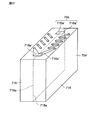
- the coil device 14 includes a helical coil 16 and a plate-like binder member (element body) 18 having a mounting surface (back surface) 18 a facing the main surface 12 a of the circuit board 12.
- the element body 18 has a rectangular parallelepiped shape, and includes a mounting surface (back surface) 18a, a top surface (main surface) 18d facing the mounting surface 18a, and two end surfaces 18e and 18f intersecting the coil axis CA of the helical coil 16. And end faces 18b and 18c along the coil axis CA.
- the mounting surface 18a is a mounting surface when the coil device is mounted on the mother board.
- the areas of the mounting surface 18a and the top surface 18d are larger than the areas of the end surfaces 18b and 18c and the end surfaces 18e and 18f.
- the element body 18 is formed in a flat plate shape (thin plate shape) in which the length (thickness) in the Z-axis direction is shorter than the lengths in the X-axis direction and the Y-axis direction.
- the end surfaces 18b and 18c have a larger area than the end surfaces 18e and 18f, but the end surfaces 18e and 18f may have a larger area than the end surfaces 18b and 18c. Good.
- the helical coil 16 extends between the mounting surface 18a and the top surface 18d, that is, along the circuit board 12 (its main surface 12a), for example, parallel to the circuit board 12. And a coil axis CA extending in the X-axis direction. That is, the conductor constituting the helical coil 16 extends helically about the coil axis CA.
- the coil axis CA is parallel to the mounting surface 18a, but is not necessarily parallel.
- the helical coil 16 is composed of a plurality of first to fourth conductors 16a to 16d.
- the plurality of first conductors 16 a are arranged on the mounting surface 18 a side of the element body 18 (that is, along the mounting surface 18 a) in the extending direction of the coil axis CA (X-axis direction). ) Are arranged at equal intervals.
- each of the plurality of first conductors 16a is parallel to each other and extends in parallel (Y-axis direction) with respect to the mounting surface 18a (that is, the circuit board 12) to have a circular cross section.
- the metal pin is a cylindrical metal column made of, for example, a copper material.
- the diameter of the circular cross section of the metal pin is, for example, 30 ⁇ m to 1 mm.
- the plurality of second conductors 16b are separated from the main surface 12a of the circuit board 12 as compared to the plurality of first conductors 16a, that is, positions separated from the mounting surface 18a of the element body 18 facing the circuit board 12.
- the element bodies 18 are arranged at equal intervals in the extending direction (X-axis direction) of the coil axis CA on the top surface 18d side (that is, along the top surface 18d).
- each of the plurality of second conductors 16b is parallel to each other and extends in parallel (Y-axis direction) with respect to the mounting surface 18a (that is, the circuit board 12) to have a circular cross section. It is a metal pin provided.
- the metal pin is a cylindrical metal column made of, for example, a copper material.
- the diameter of the circular cross section of the metal pin is, for example, 30 ⁇ m to 1 mm.
- the plurality of first conductors 16a and the plurality of second conductors 16b are the same metal pin. Therefore, the manufacturing cost of the coil device 14 can be reduced compared to the case where the first conductor 16a and the second conductor 16b are different metal pins.
- Each of the plurality of third conductors 16c is on one side with respect to the coil axis CA (on the positive side in the Y-axis direction) when viewed in a direction (Z-axis direction) orthogonal to the mounting surface 18a (that is, the main surface 12a of the circuit board 12).
- the end of the first conductor 16a and the end of the second conductor 16b are connected.
- Each of the plurality of fourth conductors 16d has a first conductor 16a on one side with respect to the coil axis CA (on the negative side in the Y-axis direction) when viewed in a direction orthogonal to the mounting surface 18a (that is, the main surface 12a of the circuit board 12). And the end of the second conductor 16b are connected.
- the plurality of first conductors 16 a and the plurality of second conductors 16 b of the helical coil 16 are included in the element body 18.
- the element body 18 has a flat plate shape and is made of a resin material such as an epoxy resin.
- each of the plurality of first conductors 16a is maintained in a state of being arranged at equal intervals in the extending direction (X-axis direction) of the coil axis CA.
- each of the plurality of second conductors 16b is also maintained in a state of being arranged at equal intervals in the extending direction of the coil axis CA.
- a plurality of third and fourth conductors 16c and 16d are provided on the end faces 18b and 18c (end faces in the Y-axis direction) of the flat plate-like element 18.
- the plurality of third and fourth conductors 16 c and 16 d are configured by conductive patterns formed on the end faces 18 b and 18 c of the element body 18, for example.
- connection terminals 20 that are electrically connected to the terminals 12d on the main surface 12a of the circuit board 12 via the conductive bonding material 22 such as solder are provided on the end faces 18b and 18c of the element body 18. Each is provided.
- the connection terminal 20 is connected to one end (the third conductor 16c or the fourth conductor 16d) of the first conductor 16a ′ on both sides of the extending direction (X-axis direction) of the coil axis CA in the plurality of first conductors 16a. Not connected to the end). That is, one connection terminal 20 is connected to one terminal of the helical coil 16, and the other connection terminal 20 is connected to the other terminal of the helical coil 16.
- one coil opening of the helical coil 16 faces the inside of the circuit board 12 at the end of the main surface 12a of the circuit board 12, and the other coil opening is a circuit. It is preferable to mount the board 12 so that it faces the outside.
- the coil device 14 is arranged so that the coil axis CA of the helical coil 16 intersects the side between the main surface 12a of the circuit board 12 and the end surface 12e (end surface in the X-axis direction). It is mounted on the main surface 12 a of the circuit board 12.
- the magnetic field (broken line) generated from the helical coil 16 is generated above the main surface 12a of the circuit board 12 on which the coil device 14 is mounted. To spread. At the same time, the magnetic field spreads to the end face 12e side. Further, the magnetic field generated by the helical coil 16 is not easily canceled by the ground layer 12b. Thereby, compared with the case where the coil device 14 is provided in the center side of the main surface 12a of the circuit board 12, the communicable range of the wireless communication device 10 is expanded and the communication distance is increased.
- the magnetic field generated from the helical coil 16 of the coil device 14 is interrupted by the ground layer 12b in the circuit board 12 and the wiring pattern (not shown) on the main surface 12a. 12 can hardly spread on the back surface 12c side. That is, the communication distance can be increased by using a metal body such as a ground layer provided on the circuit board 12.
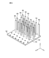
- a plurality of metal pins 50 having the same shape are erected on a pin support base 52 so as to be arranged in a plurality of rows in a direction (t-axis direction) orthogonal to the longitudinal direction (u-axis direction). It is done.
- the metal pin 50 may be fixed to the support base 52 using, for example, an adhesive such as an epoxy resin.
- a resin block 54 containing a plurality of metal pins 50 is formed on the pin support base 52.
- the resin block 54 is produced, for example, by flowing an uncured resin on the pin support base 52 and curing it by heating.
- the upper and lower sides of the resin block 54 in the drawing are polished so that both ends of the plurality of metal pins 50 in the longitudinal direction (u-axis direction) are exposed from the resin block 54.
- the upper and lower surfaces are flattened and the cueing of the metal pins is performed, so that a plurality of first conductors 16a and a plurality of second conductors 16b enclosed in the resin block 54 are produced.
- the metal pin 50 itself is not shown, and only the exposed end face is shown.
- a plurality of first conductors 16 a and a plurality of second conductors 16 b are exposed on one polishing surface 54 a of the resin block 54 where one end face is exposed.
- the third conductor 16c and the connection terminal 20 are patterned.
- the plurality of fourth conductors 16d are connected to the other polished surface 54b of the resin block 54 where the other end surfaces of the plurality of first conductors 16a and the other end surfaces of the plurality of second conductors 16b are exposed.
- the terminal 20 is patterned.
- the third conductor 16c, the fourth conductor 16d, and the connection terminal 20 are formed by forming a metal layer (for example, a copper layer) on the polished surfaces 54a and 54b of the resin block 54, and then photoetching the metal layer. It is produced by.
- the conductive paste is produced by screen-printing a predetermined pattern and heat-treating it.
- a plated film such as nickel-gold or tin may be formed on the surface of the metal layer after patterning.
- the several coil device 14 is produced by cut
- the helical coil 16 of the coil device 14 most of the plurality of conductor portions along the mounting surface 18 a and the top surface 18 d of the flat plate-like element 18, that is, the helical coil, are used.
- a plurality of conductor portions that occupy are formed of metal pins that are more rigid than wires.
- the increase in the pure resistance (DC resistance; Rdc) caused by the skin effect is suppressed for the plurality of second conductors 16b far from the mounting surface 18a by contributing to communication.
- variations in the magnetic field distribution can be suppressed.
- variation in the communicable distance of the coil device 14 that functions as an antenna can be suppressed.
- the coil device 14 transmits and receives a high-frequency signal as an antenna, a skin effect occurs in the helical coil 16 of the coil device 14.
- the skin effect means that when alternating current flows through a conductor, current does not flow uniformly over the entire conductor, but current flows intensively on the surface. Specifically, current flows through a portion of the conductor from the surface to a predetermined depth (skin depth).
- the skin depth varies depending on the conductor material and current frequency. The higher the frequency, the shallower the skin depth (ie, the higher the net resistance of the conductor).
- the material of the conductor for example, copper has a deeper skin depth (small pure resistance) than silver, and gold has a deeper skin depth (small pure resistance) than copper.
- the cross section of the conductor is rectangular, current flows concentrated on the surface on the short side.
- the cross section has a shape with a corner (for example, a triangle), the current flows concentrated on the corner. Therefore, in order for current to flow through the entire surface of the conductor, that is, in order to suppress an increase in the pure resistance of the conductor due to the skin effect, the conductor has a circular cross section.
- the plurality of conductor portions on the side farther from the mounting surface 18a (that is, the circuit board 12) in the helical coil 16 of the coil device 14 according to Embodiment 1 contributes greatly to communication.
- the plurality of second conductors 16b are formed of a plurality of metal pins having a circular cross section.
- the coil device 14 distributes a magnetic field above the main surface 12a of the circuit board 12 as shown in FIG. At this time, the second conductor 16b farther from the mounting surface 18a (that is, the circuit board 12) than the other conductors greatly contributes to this magnetic field distribution.
- the second conductor 16b In order for the second conductor 16b that greatly contributes to the magnetic field distribution to generate a magnetic field efficiently, that is, to suppress an increase in the pure resistance due to the skin effect, the second conductor 16b is composed of a metal pin having a circular cross section.
- the second conductor 16b is not a flexible metal material such as a wire, but is formed of a rigid metal pin. Therefore, it is hard to be deformed as compared with the case where the wire is configured. Accordingly, the variation in the gap between the second conductors 16b is small, and therefore, the magnetic field distribution and the self-resonance frequency of the helical coil 16 are unlikely to vary. As a result, the helical coil 16 including the second conductor 16b, that is, the coil device 14 serving as an antenna, has small variations in the communicable distance and frequency characteristics.
- the second conductor 16 b is included in the element body 18. Therefore, the deformation of the second conductor 16b is further suppressed, and the gap between the second conductors 16b is kept constant. Thereby, the variation in the magnetic field distribution of the helical coil 16 is further reduced.
- the distance between the lines is likely to vary due to the flow of the resin during sealing, and in some cases, the wire may be disconnected.
- the first conductor 16a is also composed of a metal pin having a circular cross section, like the second conductor 16b. Therefore, also for the first conductor 16a, an increase in pure resistance due to the skin effect is suppressed. Therefore, signal attenuation and power loss are also suppressed in the first conductor 16a.
- the element body 18 is a flat rectangular parallelepiped, and the first conductor 16a and the second conductor 16b are the longest conductors of the first to fourth conductors 16a to 16d constituting the helical coil 16. is there. Therefore, most of the coils can be formed of metal pins, and the coil device functions as an antenna with a small loss and a large communication distance.
- the distance D2 from the metal pin on one side to the metal pin on the other side in the coil axis extending direction is the first conductor.
- the plurality of metal pins constituting the portion 16a are configured to be shorter than the distance D1 from one metal pin in the coil axis extending direction to the other metal pin. Therefore, compared with the case where these distances D1 and D2 are equal, the coil opening area of the helical coil 16 can be increased, the coil opening can be directed to the top surface side, and the communication distance in the top surface direction. Can be increased.
- FIG. 6 is a cross-sectional view of a part of a wireless communication device having a coil device as an antenna according to the second embodiment.
- the helical coil 116 of the coil device 114 is similar to the helical coil 16 of the first embodiment described above, and includes a plurality of first coils included in the element body 118. Conductor 116a and a plurality of second conductors 116b.
- the plurality of first conductors 116a of the helical coil 116 are arranged at equal intervals in the extending direction (X-axis direction) of the coil axis CA, specifically, at a predetermined pitch interval p1.
- the plurality of second conductors 116b are located farther from the main surface 112a of the circuit board 112 (that is, the surface of the element body 118 (mounting surface) facing the main surface 112a) than the plurality of first conductors 116a.
- they are arranged at equal intervals in the extending direction of the coil axis CA, specifically at a predetermined pitch interval p2.
- the pitch interval p1 between the plurality of first conductors 116a and the pitch interval p2 between the plurality of second conductors 116b are the same.
- the pitch intervals p1 and p2 are the same, the distance (gap) g1 between the first conductors 116a adjacent to each other in the extending direction (X-axis direction) of the coil axis CA and the extending direction of the coil axis CA are the same.
- the distance (gap) g2 between the adjacent second conductors 116b is different. Specifically, the gap g2 of the second conductor 116b is narrower than the gap g1 of the first conductor 116a.
- the length in the extending direction (X-axis direction) of the coil axis CA of the cross section of the second conductor 116b (ie, the X-axis direction)
- the diameter d2) is larger than the length (diameter d1) in the extending direction of the coil axis CA of the first conductor 116a. That is, the metal pin used for the second conductor 116b is thicker than the metal pin used for the first conductor 116a.
- the magnetic field of the helical coil 116 can be greatly expanded.
- the magnetic flux generated by one of the adjacent second conductors 116b through the gap g2 and passing through the gap g2 is generated by the other and passed through the gap g2. It is suppressed that it is canceled by.
- the power supplied to the helical coil 116 is reduced to a magnetic field for wireless communication. It is used effectively in the formation of As a result, the coil device 114 including such a helical coil 116 is highly energy efficient.
- the helical coil 116 of the coil device 114 contributes to communication, and a plurality of them on the side far from the mounting surface (the main surface 112a of the circuit board 112).
- the second conductor 116b variation in the magnetic field distribution can be suppressed while suppressing an increase in pure resistance caused by the skin effect.
- the coil device 114 can form a magnetic field for wireless communication efficiently in energy.
- the helical coil 216 of the coil device 214 is similar to the helical coil 16 of the first embodiment described above, and includes a plurality of first coils included in the element body 218. Conductor 216a and a plurality of second conductors 216b.
- the plurality of first conductors 216a of the helical coil 216 are arranged at equal intervals in the extending direction (X-axis direction) of the coil axis CA, specifically, at a predetermined pitch interval p1 '.
- the plurality of second conductors 216b are located farther from the main surface 212a of the circuit board 212 (that is, the surface (mounting surface) of the element body 218 facing the main surface 212a) than the plurality of first conductors 216a.
- they are arranged at equal intervals in the extending direction of the coil axis CA, specifically, at a predetermined pitch interval p2 ′.
- the diameter d1 'of the first conductor 216a and the diameter d2' of the second conductor 216b are the same.
- the distance (gap) g2 ′ is different. Specifically, the gap g2 'of the second conductor 216b is narrower than the gap g1' of the first conductor 216a.
- the pitch interval p2 ′ of the plurality of second conductors 116b is set to the pitch of the plurality of first conductors 216a. Narrower than the interval p1 ′.
- the magnetic field of the helical coil 216 can be greatly expanded.
- the magnetic flux generated by one of the adjacent second conductors 216b through the gap g2 ′ and passing through the gap g2 ′ Is prevented from being canceled by the magnetic flux passing through the gap g2 ′.
- the electric power supplied to the helical coil 216 is effectively used for forming a magnetic field for wireless communication.
- the coil device 214 including such a helical coil 216 is highly energy efficient.
- the helical coil 216 of the coil device 214 contributes to communication, and a plurality of them on the side far from the mounting surface (the main surface 212a of the circuit board 212).
- the second conductor 216b variation in the magnetic field distribution can be suppressed while suppressing an increase in pure resistance caused by the skin effect.
- the coil device 214 can form a magnetic field for wireless communication efficiently in energy.
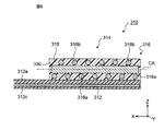
- the coil device 314 according to the fourth embodiment includes a magnetic body 330 unlike the coil device 14 according to the first embodiment.
- the magnetic body 330 is, for example, a magnetic body made of ferrite ceramic or a magnetic body in which ferrite powder is dispersed in a resin and has a flat plate shape.
- the magnetic body 330 is also included in the element body 318 in a state of being disposed in the helical coil 316. That is, the magnetic body 330 is disposed between the plurality of first conductors 316a and the plurality of second conductors 316b of the helical coil 316, and the plurality of first conductors 316a and the plurality of second conductors are arranged. It is held at 316b.
- the magnetic field of the helical coil 316 spreads over a wide range.
- the communicable distance of the wireless communication device 310 including such a coil device 314 as an antenna is increased.
- the helical coil 316 of the coil device 314 contributes to communication, and a plurality of components on the side far from the mounting surface (the main surface 312a of the circuit board 312).
- the second conductor portion 316b variation in the magnetic field distribution can be suppressed while suppressing an increase in pure resistance caused by the skin effect.
- the wireless communication device 310 can have a long communicable distance.
- the flat magnetic body 330 is held by the plurality of first conductors 316a and the plurality of second conductors 316b, the magnetic body 330 is formed when resin is flowed to form the element body 318. Therefore, it is difficult to move, and a coil device with less manufacturing variation can be configured.
- the coil device 14 includes the helical coil 16 on the end surfaces 18b and 18c (end surfaces in the Y-axis direction) that do not face the main surface 12a of the circuit board 12.
- a connection terminal 20 for electrically connecting the terminal 12d on the circuit board 12 is provided.
- the connection terminal 20 is electrically connected to the terminal 12d of the circuit board 12 via a conductive bonding material 22 such as solder.
- the coil device 414 includes a connection terminal 420 on the mounting surface 418 a facing the main surface 412 a of the circuit board 412.
- connection terminals 420 are respectively constituted by first conductors 416a 'on both sides of the extending direction (X-axis direction) of the coil axis CA in the plurality of first conductors 416a.
- the first conductors 416a ′ on both sides in the extending direction (X-axis direction) of the coil axis CA are, for example, metal pins that are thicker than the other first conductors 416a, and have a substantially semicircular cross section, that is, a plane. Is provided.
- the plane is exposed to the outside of the element body 318 by the mounting surface 418a of the element body 418 and functions as the connection terminal 420 of the coil device 414. It is preferable that a plating film is also formed on the surface of the connection terminal 420.
- a terminal 412d is provided on the main surface 412a of the circuit board 412 so as to face the connection terminal 420 (the plane of the first conductor 416a ') of the coil device 414.
- connection terminal 420 of the coil device 414 and the terminal 412d of the circuit board 412 come into contact with each other.
- a so-called LGA type terminal electrode can be formed, and the helical coil 416 of the coil device 414 and the terminal 412d of the circuit board 412 can be connected via a conductive bonding material such as solder.
- connection terminal 420 configured by the plane of the first conductor 416 a ′ is a resin block that includes the first conductor 416 a (416 a ′) and the second conductor 416 b.
- 454 is made by cutting across the first conductor 416a ′. That is, the cut surface of the resin block 454 becomes the mounting surface 418a of the element body 418, and the cut surface of the metal pin becomes the terminal surface.
- the helical coil 416 of the coil device 410 contributes to communication and the plurality of second conductors 416b on the side far from the mounting surface 418a, While suppressing an increase in pure resistance due to the skin effect, variations in magnetic field distribution can be suppressed. Further, the helical coil 416 of the coil device 414 and the terminal 412d on the circuit board 412 can be easily connected.
- the metal pin constituting the first conductor 416a ′ has a larger diameter than the metal pin constituting the other first conductor 416a. Also good.
- the first conductor 516a of the helical coil 516 is different from the first embodiment, and unlike the second conductor 516b, the rectangular cross section It is comprised with the metal member provided with.
- the first conductor 516 a is provided not on the inside of the element body 518 but on the mounting surface 518 a of the element body 518 facing the main surface 512 a of the circuit board 512.
- the first conductor 516 a is a conductive pattern formed on the mounting surface 518 a of the element body 518.
- the distribution of the magnetic field upward of the main surface 512a of the circuit board 512 is large for the second conductor 516b having a circular cross section aligned in the extending direction (X-axis direction) of the coil axis CA at a position away from the circuit board 512. Contribute. Therefore, even if each of the plurality of first conductors 516a arranged in the extending direction of the coil axis CA in the vicinity of the circuit board 512 has a rectangular shape with a higher pure resistance than a circular shape, the element body 518 There is no big impact even if outside.
- the coil device manufacturing method has a high degree of freedom.
- the plurality of first conductors 516a of the helical coil 516 may be formed not on the element body 518 of the coil device 514 but on the main surface 512a of the circuit board 512.
- the circuit board 512 includes a plurality of first conductors 516a arranged in parallel on the main surface 512a (in the X-axis direction).
- the element body 518 includes a plurality of second conductors 516b, a plurality of third conductors 516c, and a plurality of fourth conductors. That is, there are a plurality of semicircular conductors that are open on the mounting surface 518a side, and each of the plurality of semicircular conductors is a first conductor composed of a second conductor 516b, a third conductor 516c, and a plurality of fourth conductors.
- the conductors 516a are arranged in the parallel direction (X-axis direction).
- the element body 518 is mounted on the circuit board 512 such that the plurality of third conductors 516c and the plurality of fourth conductors on the element body 518 are connected to the plurality of first conductors 516a on the circuit board 512.
- the coil device 514 provided with the helical coil 516 is comprised. That is, the element body 518 including a plurality of semi-annular conductors is a surface-mounted component that is mounted on the circuit board 512 as a part of the coil device 514.
- the element body 518 and the circuit board 512 constitute a wireless communication device 510. Note that the plurality of first conductors 516a on the circuit board 512, the plurality of third conductors 516c and the plurality of fourth conductors on the element body 518 are connected by a conductive bonding material such as solder.
- the helical coil 516 of the coil device 514 contributes to communication and the plurality of second conductors 516b far from the mounting surface 518a are While suppressing an increase in pure resistance due to the skin effect, variations in magnetic field distribution can be suppressed.
- a plurality of first conductors 516 a may be formed on the mounting surface side of the element body 518.
- patterning may be performed by screen printing of a conductive paste, or patterning may be performed by etching a whole surface metal film or the like.
- the seventh embodiment is a wireless communication device different from the wireless communication device of the first embodiment. Therefore, description of the detailed configuration of the coil device is omitted.
- FIG. 12 shows a wireless communication device 600 such as a mobile terminal having the coil device 14 according to the first embodiment as an antenna.
- FIG. 13 shows a cross-sectional view of the wireless communication device 600.
- the wireless communication device 600 has a housing 602, and the coil device 14 and the circuit board 604 are accommodated in the housing 602.
- booster antenna (coil antenna) 608 having a resonance frequency of HF band is housed in the housing 602.
- the booster antenna 608 includes a first coil pattern 610, a second coil pattern 612, and an insulating plate 614 that is interposed between and supports them.
- the first coil pattern 610 and the second coil pattern 612 are rectangular spirals, and are formed on the insulating plate 614, for example.
- the opening of the first and second coil patterns 610 and 612 is larger than the opening of the helical coil in the coil device 14.
- the first and second coils are capacitively coupled when current flows in the clockwise direction when viewed in the direction orthogonal to the insulating plate 614 (Z-axis direction).
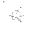
- Patterns 610 and 612 are formed. Accordingly, a stray capacitance is formed between the first coil pattern 610 and the second coil pattern 612. Therefore, as shown in FIG. 15, the inductance L1 of the first coil pattern 610, the inductance L2 of the second coil pattern 612, and the stray capacitance C1 between the terminals of the first and second coil patterns 610 and 612,
- a resonance circuit is configured by C2.
- the booster antenna 608 is configured such that the resonance frequency of the resonance circuit is a frequency in the HF band of a signal transmitted and received by the coil device 14, for example, 13.56 MHz.
- the booster antenna 608 is also arranged so as not to overlap the battery 605 and to be located in a part of the first and second coil patterns 610 and 612 in the magnetic field (broken line) generated from the coil device 14. Housed in the body 602. As a result, magnetic coupling occurs between the coil device 14 (helical coil therein) and the booster antenna 608, and a current flows through the circuit of the booster antenna 608. Since the opening of the first and second coil patterns 610 and 612 of the booster antenna 608 is larger than the opening of the helical coil in the coil device 14, a wider magnetic field is formed compared to the case of the coil device 14 alone. . As a result, the communicable distance of the wireless communication device 600 becomes longer.
- the eighth embodiment is an improved form of the fifth embodiment described above. Therefore, the eighth embodiment will be described with a focus on differences from the fifth embodiment.
- the first conductor 416a ′ which is a metal pin having a circular cross section, is cut along a plane including the central axis of the metal pin.
- the rectangular cut surface is used as the connection terminal 420.
- the first conductor 416 ' is a metal pin having a circular cross section
- the size of the cut surface may vary. That is, when the metal pin is cut off from the central axis of the metal pin, the size of the cut surface changes according to the distance from the central axis.
- the impedance at the connection terminal 420 varies, and as a result, the communication characteristics of the wireless communication device also vary.
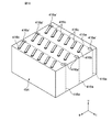
- the rectangular parallelepiped metal block 756 in the resin block 754 is cut in half, and the two first conductors 716 a ′ are cut. Is made. Thereby, a cut surface, that is, a connection terminal 720 is formed.
- the terminal surface of the connection terminal 720 can have a certain size without variation. As a result, a wireless communication device in which variations in communication characteristics are suppressed can be realized.
- the coil device 14 is mounted on a circuit board 12 that is larger than the coil device 14 as shown in FIG. Thereby, a relatively large wireless communication device 10 is configured.
- the coil device is mounted on a circuit board having the same or smaller size.
- a circuit board is mounted on the coil device, thereby forming a relatively small wireless communication device.
- FIG. 18 shows a wireless communication device 810 according to the ninth embodiment.
- the wireless communication device 810 is an RFID (Radio Frequency Identification) tag.
- the wireless communication device 810 includes the coil device 414 of the above-described fifth embodiment and the circuit board 830 mounted thereon.
- the circuit board 830 includes, for example, a flexible board 832 made of a thermoplastic resin, and an RFIC (RadioRadFrequency Integrated Circuit) element 834 mounted on a main surface 832a of the substrate 832.
- RFIC RadioRadFrequency Integrated Circuit
- two capacitor elements 836 and 838 are mounted on the main surface 832a of the substrate 832.
- the RFIC element 834, the capacitor element 836, the capacitor element 838, and the helical coil 416 of the coil device 414 constitute an RFID circuit.
- connection terminal 420 on the mounting surface 418a of the coil device 414 and the connection terminal 832c on the back surface 832b of the substrate 832 are electrically connected. These connection terminals 832c are connected to the RFIC element 834 as shown in FIG.
- a capacitor pattern may be provided on the substrate 832 instead of the capacitor elements 836 and 838.
- the wireless communication device according to the tenth embodiment is an RFID tag as in the ninth embodiment. Therefore, the points different from the ninth embodiment will be mainly described.
- a wireless communication device 910 includes the coil device 414 of the fifth embodiment described above and a circuit board 930 mounted thereon.
- the circuit board 930 includes, for example, a flexible board 932 made of a thermoplastic resin, and an RFIC (Radio Frequency Integrated Circuit) element 934 built in the board 932, as well as the board.
- 932 includes two capacitor elements 936 and 938.
- the RFIC element 934, the capacitor element 036, the capacitor element 938, and the helical coil 416 of the coil device 414 constitute an RFID circuit.
- the circuit board 930 has a plurality of connection terminals 932d to 932g for electrically connecting an external control circuit, a power supply circuit, and the like to the RFIC element 934.
- the plurality of connection terminals 932 d to 932 g are provided on the main surface 932 a of the substrate 32.
- connection terminal 420 on the mounting surface 418a of the coil device 414 and the connection terminal 932c on the back surface 932b of the substrate 932 are electrically connected. These connection terminals 932c are connected to the RFIC element 934 as shown in FIG.
- capacitor pattern may be provided on the substrate 932 instead of the capacitor elements 936 and 938.
- the coil device according to the embodiment of the present invention is used in a wireless communication device as an antenna.
- the eleventh embodiment is an electronic device that uses the coil device for purposes other than the antenna.
- FIG. 22 shows a DC-DC converter module which is an example of the electronic device according to the eleventh embodiment of the present invention.
- a DC-DC converter module 1010 includes the coil device 414 of Embodiment 5 described above and a circuit board 1030 mounted thereon.
- the circuit board 1030 includes, for example, a flexible substrate 1032 made of a thermoplastic resin, a switching IC element 1034 incorporated in the substrate 1032, and a substrate 1032 similarly.
- Two capacitor elements 1036 and 1038 are provided.
- the switching IC element 1034, the capacitor element 1036, the capacitor element 1038, and the helical coil 416 of the coil device 414 constitute a DC-DC converter circuit.
- the helical coil 416 functions as a choke coil.
- the circuit board 1030 has a plurality of connection terminals 1032d to 1032j for grounding the switching IC element 1034 and for connecting to an external control circuit, power supply circuit, and the like.
- the plurality of connection terminals 1032d to 1032j are provided on the main surface 1032a of the substrate 1032.
- the back surface 1032b of the substrate 1032 is bonded to the mounting surface 418a of the coil device 414 (the back surface of the element body 418).
- the connection terminal 420 on the mounting surface 418a of the coil device 414 and the connection terminal 1032c on the back surface 1032b of the substrate 1032 are electrically connected.
- These connection terminals 1032c are connected to the switching IC element 1034 as shown in FIG.
- capacitor pattern may be provided on the substrate 1032 instead of the capacitor elements 1036 and 1038.
- the coil device is mounted on the circuit board on the back surface thereof. That is, the coil device is mounted on the circuit board via a relatively large surface (compared to the end face) in the flat element body.
- the coil device is mounted (bonded) to the circuit board at its end face. That is, the end surface of the flat element body is used as a mounting surface of the coil device.
- a wireless communication device 1110 according to the twelfth embodiment of the present invention shown in FIG. 24 is specifically an RFID tag including the same RFID circuit (see FIG. 19) as that of the ninth embodiment.
- a wireless communication device 1110 includes a coil device 1114 having a helical coil and a circuit board 1130 mounted thereon.
- the coil device 1114 includes connection terminals 1120 connected to both ends of the helical coil on the end surface 1118b instead of the back surface 1118a of the flat plate-like element body 1118 and not the main surface 1118d. .
- the circuit board 1130 includes, for example, a flexible board 1132 made of a thermoplastic resin, an RFIC element 1134 mounted on the main surface 1132a of the board 1132, and similarly mounted on the main surface 1132a of the board 1132. Two capacitor elements 1136 and 1138 are provided.
- connection terminal 1120 on the mounting surface 1118b of the coil device 1114 and the connection terminal 1132c on the back surface 1132b of the substrate 1132 are electrically connected. These connection terminals 1132 c are connected to the RFIC element 1134.
- the wireless communication device of the thirteenth embodiment is an RFID tag including the same RFID circuit (see FIG. 21) as that of the tenth embodiment. However, the coil device is joined to the circuit board at its end face, as in the twelfth embodiment.
- the wireless communication device 1210 As shown in FIG. 25, the wireless communication device 1210 according to the thirteenth embodiment has a coil device 1214 and a circuit board 1230 mounted thereon.
- the coil device 1214 includes connection terminals 1220 connected to both ends of the helical coil on the mounting surface 1218b (end surface of the element body 1218).
- the circuit board 1230 includes, for example, a flexible substrate 1232 made of a thermoplastic resin, an RFIC element 1234 mounted on the main surface 1232a of the substrate 1232, and similarly mounted on the main surface 1232a of the substrate 1232.
- Two capacitor elements 1236 and 1238 are provided.
- connection terminal 1220 on the mounting surface 1218b of the coil device 1214 and the connection terminal 1232c on the back surface 1232b of the substrate 1232 are electrically connected. These connection terminals 1232 c are connected to the RFIC element 1234.
- connection terminals 1232d to 1232g for electrically connecting an external control circuit, a power supply circuit, and the like to the RFIC element 1234 are provided on the back surface 1232b of the substrate 1232.
- a plurality of conductors 1222 connected to the connection terminals 1232d to 1232g are provided in the coil device 1214.
- the plurality of conductors 1222 are, for example, conductor layers formed from the back surface 1218a of the element body 1218 to the end surface 1218b. Further, for example, the plurality of conductors 1222 are metal pins that are included in the element body 1218 and exposed to the outside at the back surface 1218 a and the end surface 1218 b of the element body 1218.
- an embodiment of the present invention is a helical element including a flat element body having a main surface, a back surface, and an end surface, and a coil shaft provided on the element body and extending between the main surface and the back surface.
- a conductor that is provided on the back surface or the end surface of the element body and is connected to the helical coil, and a conductor that constitutes the helical coil has a plurality of conductor portions along the main surface, It is a coil device each comprised by the metal pin.
- a coil device as an antenna is mounted on an end of a main surface of a circuit board.
- it may be mounted at another location, for example, at the center of the main surface of the circuit board.
- the first to fourth conductors of the helical coil of the coil device may be the same material or different materials.
- the metal pin of the second conductor may be made of a material having a deep skin depth.
- the metal pin of the second conductor is made of gold and the other conductor is made of copper, the helical coil can be made at a low cost while suppressing an increase in the pure resistance of the second conductor. (Compared with the case where all the helical coil conductors are made of gold).
- the plurality of first and second conductors are preferably parallel to each other.
- a plurality of metal pins can be easily set when manufacturing a coil device.
- the extending direction of the coil axis (X
- the helical coil may be configured so that the first conductor and the second conductor face each other in a direction orthogonal to the circuit board.
- the coil device according to the embodiment of the present invention as an antenna is not limited to being used for transmission / reception of HF band frequency signals, but for transmitting / receiving signals of various band frequencies. It can be used.
- the coil device according to the embodiment of the present invention as an antenna may be used for transmission / reception of a signal having a frequency in the UHF band, for example.
- a new embodiment can be realized by arranging the magnetic body 330 of the coil device 314 of the fourth embodiment in the coil device 14 of the first embodiment. Further, by applying the coil device 114 of the second embodiment to the wireless communication device 600 of the seventh embodiment, a new embodiment can be realized.
- the coil device of the present invention can be applied not only to a wireless communication device and a DC-DC converter module but also to other devices using a coil.
Landscapes
- Engineering & Computer Science (AREA)
- Power Engineering (AREA)
- Microelectronics & Electronic Packaging (AREA)
- Computer Networks & Wireless Communication (AREA)
- Coils Or Transformers For Communication (AREA)
- Coils Of Transformers For General Uses (AREA)
- Details Of Aerials (AREA)
Abstract
L'invention concerne un dispositif de bobine 14 qui comprend : un élément de type plaque 18 qui a une surface principale 18d, une surface arrière 18a et une surface d'extrémité 18b ; une bobine hélicoïdale 16 qui est disposée sur l'élément 18 et a un axe de bobine CA qui s'étend entre la surface principale 18d et la surface arrière 18a ; et une borne de connexion 20 qui est disposée sur la surface arrière 18a ou la surface d'extrémité 18b de l'élément 18 et est connectée à la bobine hélicoïdale 16. Par rapport à un conducteur qui constitue la bobine hélicoïdale 16, une pluralité de parties de conducteur 16b s'étendant le long de la surface principale 18d sont respectivement configurées d'une pluralité de broches métalliques.
Priority Applications (3)
| Application Number | Priority Date | Filing Date | Title |
|---|---|---|---|
| JP2017504989A JP6380648B2 (ja) | 2015-03-09 | 2016-02-29 | コイルデバイスおよび電子デバイス |
| CN201690000554.4U CN207542406U (zh) | 2015-03-09 | 2016-02-29 | 线圈装置和电子器件 |
| US15/697,663 US20170373396A1 (en) | 2015-03-09 | 2017-09-07 | Coil device and electronic device |
Applications Claiming Priority (2)
| Application Number | Priority Date | Filing Date | Title |
|---|---|---|---|
| JP2015046119 | 2015-03-09 | ||
| JP2015-046119 | 2015-03-09 |
Related Child Applications (1)
| Application Number | Title | Priority Date | Filing Date |
|---|---|---|---|
| US15/697,663 Continuation US20170373396A1 (en) | 2015-03-09 | 2017-09-07 | Coil device and electronic device |
Publications (1)
| Publication Number | Publication Date |
|---|---|
| WO2016143584A1 true WO2016143584A1 (fr) | 2016-09-15 |
Family
ID=56880381
Family Applications (1)
| Application Number | Title | Priority Date | Filing Date |
|---|---|---|---|
| PCT/JP2016/056088 Ceased WO2016143584A1 (fr) | 2015-03-09 | 2016-02-29 | Dispositif de bobine et dispositif électronique |
Country Status (4)
| Country | Link |
|---|---|
| US (1) | US20170373396A1 (fr) |
| JP (1) | JP6380648B2 (fr) |
| CN (1) | CN207542406U (fr) |
| WO (1) | WO2016143584A1 (fr) |
Cited By (3)
| Publication number | Priority date | Publication date | Assignee | Title |
|---|---|---|---|---|
| WO2017134993A1 (fr) * | 2016-02-02 | 2017-08-10 | 株式会社村田製作所 | Composant de bobine type à montage en surface ainsi que procédé de fabrication de celui-ci, et convertisseur courant continu – courant continu mettant en œuvre celui-ci |
| JP2023104202A (ja) * | 2022-01-17 | 2023-07-28 | Tdk株式会社 | 積層コイル部品 |
| TWI848547B (zh) * | 2022-03-28 | 2024-07-11 | 日商 Tdk 股份有限公司 | 電子零件 |
Families Citing this family (5)
| Publication number | Priority date | Publication date | Assignee | Title |
|---|---|---|---|---|
| CN102668241B (zh) * | 2010-03-24 | 2015-01-28 | 株式会社村田制作所 | Rfid系统 |
| KR102567364B1 (ko) * | 2016-01-27 | 2023-08-16 | 삼성전자주식회사 | 안테나 보조 장치 및 이를 포함하는 전자 장치 |
| WO2019239626A1 (fr) * | 2018-06-15 | 2019-12-19 | 株式会社村田製作所 | Étiquette rfid et son procédé de fabrication |
| CN111293420B (zh) | 2019-01-31 | 2021-04-27 | 展讯通信(上海)有限公司 | 天线单元、天线系统及电子装置 |
| KR102837229B1 (ko) * | 2020-12-23 | 2025-07-22 | (주)포인트엔지니어링 | 인덕터 및 인덕터용 바디 부재 |
Citations (11)
| Publication number | Priority date | Publication date | Assignee | Title |
|---|---|---|---|---|
| WO2002089157A1 (fr) * | 2001-04-27 | 2002-11-07 | Ajinomoto Co., Inc. | Enroulement multicouche et procede de fabrication |
| JP2004235584A (ja) * | 2003-01-31 | 2004-08-19 | Tdk Corp | インダクタンス素子と積層電子部品と積層電子部品モジュ−ルとこれらの製造方法 |
| JP2005072170A (ja) * | 2003-08-22 | 2005-03-17 | Toko Inc | チップ型電子部品 |
| JP2005184094A (ja) * | 2003-12-16 | 2005-07-07 | Olympus Corp | アンテナおよびアンテナの製造方法 |
| US20070085648A1 (en) * | 2005-10-19 | 2007-04-19 | Samsung Electronics Co., Ltd. | High efficiency inductor, method for manufacturing the inductor, and packaging structure using the inductor |
| WO2011027603A1 (fr) * | 2009-09-01 | 2011-03-10 | 横浜ゴム株式会社 | Antenne |
| JP2012104673A (ja) * | 2010-11-10 | 2012-05-31 | Tdk Corp | コイル部品及びその製造方法 |
| WO2012144482A1 (fr) * | 2011-04-18 | 2012-10-26 | 株式会社村田製作所 | Dispositif d'antenne et dispositif de terminal de communication |
| WO2013168558A1 (fr) * | 2012-05-09 | 2013-11-14 | 株式会社 村田製作所 | Élément d'antenne à cadre et module d'antenne |
| JP2014168038A (ja) * | 2013-02-04 | 2014-09-11 | Nec Tokin Corp | 磁芯、インダクタ、及びインダクタを備えたモジュール |
| WO2014199862A1 (fr) * | 2013-06-14 | 2014-12-18 | 株式会社村田製作所 | Dispositif d'antenne et dispositif de terminal de communication |
Family Cites Families (10)
| Publication number | Priority date | Publication date | Assignee | Title |
|---|---|---|---|---|
| JP2836039B2 (ja) * | 1989-12-28 | 1998-12-14 | ティーディーケイ株式会社 | インピーダンス素子 |
| US5576680A (en) * | 1994-03-01 | 1996-11-19 | Amer-Soi | Structure and fabrication process of inductors on semiconductor chip |
| JP3582256B2 (ja) * | 1996-10-23 | 2004-10-27 | 松下電器産業株式会社 | インピーダンス素子及びその製造方法 |
| US6531945B1 (en) * | 2000-03-10 | 2003-03-11 | Micron Technology, Inc. | Integrated circuit inductor with a magnetic core |
| JP3730926B2 (ja) * | 2002-03-14 | 2006-01-05 | 京セラ株式会社 | ヘリカル型アンテナの設計方法 |
| JP2006054208A (ja) * | 2002-08-29 | 2006-02-23 | Ajinomoto Co Inc | 可変インダクタンス素子、可変インダクタンス素子内蔵多層基板、半導体チップ及びチップ型可変インダクタンス素子 |
| JP2004128130A (ja) * | 2002-10-01 | 2004-04-22 | Tdk Corp | コイル部品とその製造方法 |
| US8591262B2 (en) * | 2010-09-03 | 2013-11-26 | Pulse Electronics, Inc. | Substrate inductive devices and methods |
| WO2013101131A1 (fr) * | 2011-12-29 | 2013-07-04 | Intel Corporation | Inducteur intégré pour des dispositifs à circuit intégré |
| JP2014038884A (ja) * | 2012-08-10 | 2014-02-27 | Murata Mfg Co Ltd | 電子部品および電子部品の製造方法 |
-
2016
- 2016-02-29 JP JP2017504989A patent/JP6380648B2/ja active Active
- 2016-02-29 WO PCT/JP2016/056088 patent/WO2016143584A1/fr not_active Ceased
- 2016-02-29 CN CN201690000554.4U patent/CN207542406U/zh not_active Expired - Lifetime
-
2017
- 2017-09-07 US US15/697,663 patent/US20170373396A1/en not_active Abandoned
Patent Citations (11)
| Publication number | Priority date | Publication date | Assignee | Title |
|---|---|---|---|---|
| WO2002089157A1 (fr) * | 2001-04-27 | 2002-11-07 | Ajinomoto Co., Inc. | Enroulement multicouche et procede de fabrication |
| JP2004235584A (ja) * | 2003-01-31 | 2004-08-19 | Tdk Corp | インダクタンス素子と積層電子部品と積層電子部品モジュ−ルとこれらの製造方法 |
| JP2005072170A (ja) * | 2003-08-22 | 2005-03-17 | Toko Inc | チップ型電子部品 |
| JP2005184094A (ja) * | 2003-12-16 | 2005-07-07 | Olympus Corp | アンテナおよびアンテナの製造方法 |
| US20070085648A1 (en) * | 2005-10-19 | 2007-04-19 | Samsung Electronics Co., Ltd. | High efficiency inductor, method for manufacturing the inductor, and packaging structure using the inductor |
| WO2011027603A1 (fr) * | 2009-09-01 | 2011-03-10 | 横浜ゴム株式会社 | Antenne |
| JP2012104673A (ja) * | 2010-11-10 | 2012-05-31 | Tdk Corp | コイル部品及びその製造方法 |
| WO2012144482A1 (fr) * | 2011-04-18 | 2012-10-26 | 株式会社村田製作所 | Dispositif d'antenne et dispositif de terminal de communication |
| WO2013168558A1 (fr) * | 2012-05-09 | 2013-11-14 | 株式会社 村田製作所 | Élément d'antenne à cadre et module d'antenne |
| JP2014168038A (ja) * | 2013-02-04 | 2014-09-11 | Nec Tokin Corp | 磁芯、インダクタ、及びインダクタを備えたモジュール |
| WO2014199862A1 (fr) * | 2013-06-14 | 2014-12-18 | 株式会社村田製作所 | Dispositif d'antenne et dispositif de terminal de communication |
Cited By (5)
| Publication number | Priority date | Publication date | Assignee | Title |
|---|---|---|---|---|
| WO2017134993A1 (fr) * | 2016-02-02 | 2017-08-10 | 株式会社村田製作所 | Composant de bobine type à montage en surface ainsi que procédé de fabrication de celui-ci, et convertisseur courant continu – courant continu mettant en œuvre celui-ci |
| US11387037B2 (en) | 2016-02-02 | 2022-07-12 | Murata Manufacturing Co., Ltd. | Surface mount coil component, method of manufacturing the same, and DC-DC converter using the same |
| JP2023104202A (ja) * | 2022-01-17 | 2023-07-28 | Tdk株式会社 | 積層コイル部品 |
| JP7741735B2 (ja) | 2022-01-17 | 2025-09-18 | Tdk株式会社 | 積層コイル部品 |
| TWI848547B (zh) * | 2022-03-28 | 2024-07-11 | 日商 Tdk 股份有限公司 | 電子零件 |
Also Published As
| Publication number | Publication date |
|---|---|
| JP6380648B2 (ja) | 2018-08-29 |
| US20170373396A1 (en) | 2017-12-28 |
| CN207542406U (zh) | 2018-06-26 |
| JPWO2016143584A1 (ja) | 2018-01-25 |
Similar Documents
| Publication | Publication Date | Title |
|---|---|---|
| JP6380648B2 (ja) | コイルデバイスおよび電子デバイス | |
| KR102047563B1 (ko) | 코일 부품 및 그 실장 기판 | |
| EP2696438B1 (fr) | Dispositif d'antenne, dispositif de communication sans fil et procédé de fabrication d'un dispositif d'antenne | |
| US10374305B2 (en) | Multilayer substrate and electronic device | |
| EP2667447B1 (fr) | Dispositif d'antenne et dispositif de communication sans fil | |
| JP5521686B2 (ja) | アンテナ装置及び無線通信デバイス | |
| US8602310B2 (en) | Radio communication device and radio communication terminal | |
| CN206727226U (zh) | 天线装置以及电子设备 | |
| CN109545503B (zh) | 电子组件 | |
| KR20160108934A (ko) | 코일 부품 및 그 실장 기판 | |
| KR102029491B1 (ko) | 코일 부품 및 그 실장 기판 | |
| KR101580401B1 (ko) | 안테나 장치, 이를 갖는 전자 부품 및 전자 기기 | |
| US9673524B2 (en) | Compact loop-type antenna device | |
| KR20160072198A (ko) | 코일 안테나의 제조 방법 및 코일 안테나 패키지의 제조 방법 | |
| JP2019008596A (ja) | 配線基板およびrfidタグ | |
| US20160351317A1 (en) | Hybrid inductor device | |
| US10122065B2 (en) | Antenna device, card information medium, electronic apparatus, and method for manufacturing antenna device | |
| WO2017150614A1 (fr) | Module de composant électronique, convertisseur cc-cc et dispositif électronique | |
| US20240186049A1 (en) | Coil element, antenna device, and electronic device | |
| JP2013247554A (ja) | アンテナ装置および通信端末装置 | |
| US20200074263A1 (en) | Rfic module, rfid tag, and article | |
| WO2017033698A1 (fr) | Élément bobine, dispositif d'antenne, support d'informations du type carte, dispositif de circuit intégré sans fil et dispositif électronique | |
| JP7733359B2 (ja) | Rfidモジュール | |
| US20250117621A1 (en) | Rfid module | |
| JP2005217633A (ja) | アンテナ装置 |
Legal Events
| Date | Code | Title | Description |
|---|---|---|---|
| 121 | Ep: the epo has been informed by wipo that ep was designated in this application |
Ref document number: 16761554 Country of ref document: EP Kind code of ref document: A1 |
|
| ENP | Entry into the national phase |
Ref document number: 2017504989 Country of ref document: JP Kind code of ref document: A |
|
| NENP | Non-entry into the national phase |
Ref country code: DE |
|
| 122 | Ep: pct application non-entry in european phase |
Ref document number: 16761554 Country of ref document: EP Kind code of ref document: A1 |