WO2017134993A1 - Composant de bobine type à montage en surface ainsi que procédé de fabrication de celui-ci, et convertisseur courant continu – courant continu mettant en œuvre celui-ci - Google Patents
Composant de bobine type à montage en surface ainsi que procédé de fabrication de celui-ci, et convertisseur courant continu – courant continu mettant en œuvre celui-ci Download PDFInfo
- Publication number
- WO2017134993A1 WO2017134993A1 PCT/JP2017/000651 JP2017000651W WO2017134993A1 WO 2017134993 A1 WO2017134993 A1 WO 2017134993A1 JP 2017000651 W JP2017000651 W JP 2017000651W WO 2017134993 A1 WO2017134993 A1 WO 2017134993A1
- Authority
- WO
- WIPO (PCT)
- Prior art keywords
- element body
- conductor pattern
- metal pins
- metal
- coil
- Prior art date
- Legal status (The legal status is an assumption and is not a legal conclusion. Google has not performed a legal analysis and makes no representation as to the accuracy of the status listed.)
- Ceased
Links
Images




Classifications
-
- H—ELECTRICITY
- H01—ELECTRIC ELEMENTS
- H01F—MAGNETS; INDUCTANCES; TRANSFORMERS; SELECTION OF MATERIALS FOR THEIR MAGNETIC PROPERTIES
- H01F27/00—Details of transformers or inductances, in general
- H01F27/28—Coils; Windings; Conductive connections
- H01F27/29—Terminals; Tapping arrangements for signal inductances
- H01F27/292—Surface mounted devices
-
- H—ELECTRICITY
- H01—ELECTRIC ELEMENTS
- H01F—MAGNETS; INDUCTANCES; TRANSFORMERS; SELECTION OF MATERIALS FOR THEIR MAGNETIC PROPERTIES
- H01F17/00—Fixed inductances of the signal type
- H01F17/04—Fixed inductances of the signal type with magnetic core
-
- H—ELECTRICITY
- H01—ELECTRIC ELEMENTS
- H01F—MAGNETS; INDUCTANCES; TRANSFORMERS; SELECTION OF MATERIALS FOR THEIR MAGNETIC PROPERTIES
- H01F27/00—Details of transformers or inductances, in general
- H01F27/24—Magnetic cores
-
- H—ELECTRICITY
- H01—ELECTRIC ELEMENTS
- H01F—MAGNETS; INDUCTANCES; TRANSFORMERS; SELECTION OF MATERIALS FOR THEIR MAGNETIC PROPERTIES
- H01F27/00—Details of transformers or inductances, in general
- H01F27/28—Coils; Windings; Conductive connections
-
- H—ELECTRICITY
- H01—ELECTRIC ELEMENTS
- H01F—MAGNETS; INDUCTANCES; TRANSFORMERS; SELECTION OF MATERIALS FOR THEIR MAGNETIC PROPERTIES
- H01F27/00—Details of transformers or inductances, in general
- H01F27/28—Coils; Windings; Conductive connections
- H01F27/2804—Printed windings
-
- H—ELECTRICITY
- H01—ELECTRIC ELEMENTS
- H01F—MAGNETS; INDUCTANCES; TRANSFORMERS; SELECTION OF MATERIALS FOR THEIR MAGNETIC PROPERTIES
- H01F41/00—Apparatus or processes specially adapted for manufacturing or assembling magnets, inductances or transformers; Apparatus or processes specially adapted for manufacturing materials characterised by their magnetic properties
- H01F41/02—Apparatus or processes specially adapted for manufacturing or assembling magnets, inductances or transformers; Apparatus or processes specially adapted for manufacturing materials characterised by their magnetic properties for manufacturing cores, coils, or magnets
- H01F41/0206—Manufacturing of magnetic cores by mechanical means
-
- H—ELECTRICITY
- H01—ELECTRIC ELEMENTS
- H01F—MAGNETS; INDUCTANCES; TRANSFORMERS; SELECTION OF MATERIALS FOR THEIR MAGNETIC PROPERTIES
- H01F41/00—Apparatus or processes specially adapted for manufacturing or assembling magnets, inductances or transformers; Apparatus or processes specially adapted for manufacturing materials characterised by their magnetic properties
- H01F41/02—Apparatus or processes specially adapted for manufacturing or assembling magnets, inductances or transformers; Apparatus or processes specially adapted for manufacturing materials characterised by their magnetic properties for manufacturing cores, coils, or magnets
- H01F41/04—Apparatus or processes specially adapted for manufacturing or assembling magnets, inductances or transformers; Apparatus or processes specially adapted for manufacturing materials characterised by their magnetic properties for manufacturing cores, coils, or magnets for manufacturing coils
-
- H—ELECTRICITY
- H01—ELECTRIC ELEMENTS
- H01F—MAGNETS; INDUCTANCES; TRANSFORMERS; SELECTION OF MATERIALS FOR THEIR MAGNETIC PROPERTIES
- H01F41/00—Apparatus or processes specially adapted for manufacturing or assembling magnets, inductances or transformers; Apparatus or processes specially adapted for manufacturing materials characterised by their magnetic properties
- H01F41/02—Apparatus or processes specially adapted for manufacturing or assembling magnets, inductances or transformers; Apparatus or processes specially adapted for manufacturing materials characterised by their magnetic properties for manufacturing cores, coils, or magnets
- H01F41/04—Apparatus or processes specially adapted for manufacturing or assembling magnets, inductances or transformers; Apparatus or processes specially adapted for manufacturing materials characterised by their magnetic properties for manufacturing cores, coils, or magnets for manufacturing coils
- H01F41/041—Printed circuit coils
-
- H—ELECTRICITY
- H01—ELECTRIC ELEMENTS
- H01F—MAGNETS; INDUCTANCES; TRANSFORMERS; SELECTION OF MATERIALS FOR THEIR MAGNETIC PROPERTIES
- H01F41/00—Apparatus or processes specially adapted for manufacturing or assembling magnets, inductances or transformers; Apparatus or processes specially adapted for manufacturing materials characterised by their magnetic properties
- H01F41/02—Apparatus or processes specially adapted for manufacturing or assembling magnets, inductances or transformers; Apparatus or processes specially adapted for manufacturing materials characterised by their magnetic properties for manufacturing cores, coils, or magnets
- H01F41/04—Apparatus or processes specially adapted for manufacturing or assembling magnets, inductances or transformers; Apparatus or processes specially adapted for manufacturing materials characterised by their magnetic properties for manufacturing cores, coils, or magnets for manufacturing coils
- H01F41/041—Printed circuit coils
- H01F41/043—Printed circuit coils by thick film techniques
-
- H—ELECTRICITY
- H01—ELECTRIC ELEMENTS
- H01F—MAGNETS; INDUCTANCES; TRANSFORMERS; SELECTION OF MATERIALS FOR THEIR MAGNETIC PROPERTIES
- H01F41/00—Apparatus or processes specially adapted for manufacturing or assembling magnets, inductances or transformers; Apparatus or processes specially adapted for manufacturing materials characterised by their magnetic properties
- H01F41/02—Apparatus or processes specially adapted for manufacturing or assembling magnets, inductances or transformers; Apparatus or processes specially adapted for manufacturing materials characterised by their magnetic properties for manufacturing cores, coils, or magnets
- H01F41/04—Apparatus or processes specially adapted for manufacturing or assembling magnets, inductances or transformers; Apparatus or processes specially adapted for manufacturing materials characterised by their magnetic properties for manufacturing cores, coils, or magnets for manufacturing coils
- H01F41/10—Connecting leads to windings
-
- H—ELECTRICITY
- H02—GENERATION; CONVERSION OR DISTRIBUTION OF ELECTRIC POWER
- H02M—APPARATUS FOR CONVERSION BETWEEN AC AND AC, BETWEEN AC AND DC, OR BETWEEN DC AND DC, AND FOR USE WITH MAINS OR SIMILAR POWER SUPPLY SYSTEMS; CONVERSION OF DC OR AC INPUT POWER INTO SURGE OUTPUT POWER; CONTROL OR REGULATION THEREOF
- H02M3/00—Conversion of DC power input into DC power output
- H02M3/003—Constructional details, e.g. physical layout, assembly, wiring or busbar connections
-
- H—ELECTRICITY
- H01—ELECTRIC ELEMENTS
- H01F—MAGNETS; INDUCTANCES; TRANSFORMERS; SELECTION OF MATERIALS FOR THEIR MAGNETIC PROPERTIES
- H01F17/00—Fixed inductances of the signal type
- H01F17/04—Fixed inductances of the signal type with magnetic core
- H01F2017/048—Fixed inductances of the signal type with magnetic core with encapsulating core, e.g. made of resin and magnetic powder
-
- H—ELECTRICITY
- H01—ELECTRIC ELEMENTS
- H01F—MAGNETS; INDUCTANCES; TRANSFORMERS; SELECTION OF MATERIALS FOR THEIR MAGNETIC PROPERTIES
- H01F27/00—Details of transformers or inductances, in general
- H01F27/28—Coils; Windings; Conductive connections
- H01F27/2804—Printed windings
- H01F2027/2814—Printed windings with only part of the coil or of the winding in the printed circuit board, e.g. the remaining coil or winding sections can be made of wires or sheets
-
- H—ELECTRICITY
- H02—GENERATION; CONVERSION OR DISTRIBUTION OF ELECTRIC POWER
- H02M—APPARATUS FOR CONVERSION BETWEEN AC AND AC, BETWEEN AC AND DC, OR BETWEEN DC AND DC, AND FOR USE WITH MAINS OR SIMILAR POWER SUPPLY SYSTEMS; CONVERSION OF DC OR AC INPUT POWER INTO SURGE OUTPUT POWER; CONTROL OR REGULATION THEREOF
- H02M3/00—Conversion of DC power input into DC power output
- H02M3/02—Conversion of DC power input into DC power output without intermediate conversion into AC
- H02M3/04—Conversion of DC power input into DC power output without intermediate conversion into AC by static converters
- H02M3/10—Conversion of DC power input into DC power output without intermediate conversion into AC by static converters using discharge tubes with control electrode or semiconductor devices with control electrode
- H02M3/145—Conversion of DC power input into DC power output without intermediate conversion into AC by static converters using discharge tubes with control electrode or semiconductor devices with control electrode using devices of a triode or transistor type requiring continuous application of a control signal
- H02M3/155—Conversion of DC power input into DC power output without intermediate conversion into AC by static converters using discharge tubes with control electrode or semiconductor devices with control electrode using devices of a triode or transistor type requiring continuous application of a control signal using semiconductor devices only
-
- H—ELECTRICITY
- H05—ELECTRIC TECHNIQUES NOT OTHERWISE PROVIDED FOR
- H05K—PRINTED CIRCUITS; CASINGS OR CONSTRUCTIONAL DETAILS OF ELECTRIC APPARATUS; MANUFACTURE OF ASSEMBLAGES OF ELECTRICAL COMPONENTS
- H05K1/00—Printed circuits
- H05K1/18—Printed circuits structurally associated with non-printed electric components
- H05K1/181—Printed circuits structurally associated with non-printed electric components associated with surface mounted components
-
- H—ELECTRICITY
- H05—ELECTRIC TECHNIQUES NOT OTHERWISE PROVIDED FOR
- H05K—PRINTED CIRCUITS; CASINGS OR CONSTRUCTIONAL DETAILS OF ELECTRIC APPARATUS; MANUFACTURE OF ASSEMBLAGES OF ELECTRICAL COMPONENTS
- H05K2201/00—Indexing scheme relating to printed circuits covered by H05K1/00
- H05K2201/10—Details of components or other objects attached to or integrated in a printed circuit board
- H05K2201/10007—Types of components
- H05K2201/10015—Non-printed capacitor
-
- H—ELECTRICITY
- H05—ELECTRIC TECHNIQUES NOT OTHERWISE PROVIDED FOR
- H05K—PRINTED CIRCUITS; CASINGS OR CONSTRUCTIONAL DETAILS OF ELECTRIC APPARATUS; MANUFACTURE OF ASSEMBLAGES OF ELECTRICAL COMPONENTS
- H05K2201/00—Indexing scheme relating to printed circuits covered by H05K1/00
- H05K2201/10—Details of components or other objects attached to or integrated in a printed circuit board
- H05K2201/10007—Types of components
- H05K2201/1003—Non-printed inductor
-
- H—ELECTRICITY
- H05—ELECTRIC TECHNIQUES NOT OTHERWISE PROVIDED FOR
- H05K—PRINTED CIRCUITS; CASINGS OR CONSTRUCTIONAL DETAILS OF ELECTRIC APPARATUS; MANUFACTURE OF ASSEMBLAGES OF ELECTRICAL COMPONENTS
- H05K2201/00—Indexing scheme relating to printed circuits covered by H05K1/00
- H05K2201/10—Details of components or other objects attached to or integrated in a printed circuit board
- H05K2201/10007—Types of components
- H05K2201/10053—Switch
Definitions
- the metal composite type coil member has, for example, a structure in which a coil such as an air-core coil is embedded in a metal composite material (a magnetic metal powder dispersed in a resin (binder)).
- the first magnetic layer and the second magnetic layer are made of a composite magnetic material in which magnetic particles are dispersed in a resin. It may be a thing.
- the surface mount coil component according to a fifth aspect is the above-described third or fourth aspect, wherein the relative magnetic permeability of the element body is equal to the relative magnetic permeability of the first magnetic layer and the second magnetic layer. It may be higher than the relative permeability.
- a DC-DC converter includes a switching element, Connected to the switching element, and a choke coil;
- the choke coil is An element body having a first surface, a second surface facing the first surface, and a third surface connecting the first surface and the second surface, and comprising a molded body including magnetic particles; , A first conductor pattern provided on the first surface of the element body; A second conductor pattern provided on the second surface of the element body; Input / output terminals provided on the third surface of the element body; A plurality of metal pins embedded in the element body, each metal pin having a first end connected to the first conductor pattern and a second end connected to the second conductor pattern; , With A coil conductor is constituted by the first conductor pattern, the second conductor pattern, and the plurality of metal pins, The input / output terminal is constituted by a pair of metal pins exposed on the third surface of the element body among the plurality of metal pins.
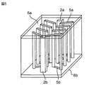
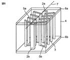
- the coil conductor is provided in the element body 4.
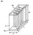
- the coil conductor includes a plurality of metal pins 2 a, 2 b, 3 embedded in the element body 4, a first conductor pattern 5 a provided on the first surface 9 a of the element body 4, And a second conductor pattern 5b provided on the second surface 9b.
- the winding axis of the coil conductor is the y axis.
- the metal pins 2a, 2b, and 3 are embedded in the element body 4. Each metal pin 2 a, 2 b, 3 has one end exposed at the first surface 9 a of the element body 4 and the other end exposed at the second surface 9 b of the element body 4.
- the metal pins 2a, 2b, and 3 extend along the z-axis direction.
- “exposed” means that one end or the other end of the metal pins 2a, 2b, 3 is flush with the first surface 9a or the second surface 9b of the element body 4, or the metal pins 2a, 2b. 3 is protruding.
- the metal pins 2a, 2b, and 3 can be metal pins mainly composed of Cu.
- the metal pins 2a, 2b, and 3 may be formed by, for example, extending a Cu-based metal block into a predetermined shape.
- the material of the metal pins 2a, 2b, and 3 is only required to have conductivity, and the material is not limited to Cu, and may be a conductive material such as Ag or Al.
- the outer diameters of the metal pins 2a, 2b, and 3 may be 0.1 mm or more and 0.5 mm or less.
- the metal pins 2a, 2b, 3 may have a length of 0.5 mm to 10 mm.
- the surface of the element body 4 in which the metal pins 2 a and 2 b are embedded may be cut out to expose the metal pins 2 a and 2 b on the third surface 9 c of the element body 4.
- the metal pins 2a, 2b, and 3 may have a surface plated with Ni / Au or the like.
- the surface of the side surface excluding one end and the other end of the metal pin 3 may be covered with an insulating film.
- the upper surface (first surface) 9a and the lower surface 9b (second surface) of the element body 4 made of a metal composite material are polished, and cueing (exposure) of the metal pins 2a, 2b, 3 is performed.
- the first conductor pattern 5a is formed on the upper surface (first surface) 9a
- the second conductor pattern 5b is formed on the lower surface (second surface) 9b (FIG. 4).
- Each conductor pattern 5a, 5b is formed by patterning and plating with a conductive paste.
- the first conductor pattern 5a and the second conductor pattern 5b may be formed only by plating, or other thin film processes may be used.
- the surface-mounted coil component according to the present invention is useful as a surface-mounted coil component that maintains the shape of the coil and has excellent coil characteristics.
Landscapes
- Engineering & Computer Science (AREA)
- Power Engineering (AREA)
- Manufacturing & Machinery (AREA)
- Microelectronics & Electronic Packaging (AREA)
- Coils Or Transformers For Communication (AREA)
- Manufacturing Cores, Coils, And Magnets (AREA)
- Dc-Dc Converters (AREA)
Abstract
Selon un premier mode de réalisation de l'invention, un composant de bobine type à montage en surface est équipé : d'un corps d'élément qui possède une première face, une seconde face s'opposant à la première face, et une troisième face raccordant la première et la seconde face, et qui est constitué par un corps moulé contenant des particules magnétiques ; d'un premier motif conducteur agencé sur la première face du corps d'élément ; d'un second motif conducteur agencé sur la seconde face du corps d'élément ; d'une borne d'entrée et sortie agencée sur la troisième face du corps d'élément ; et d'une pluralité de broches métalliques qui sont noyées dans le corps d'élément, chacune présentant une extrémité connectée à un premier motif conducteur, et une autre extrémité connectée à un second motif conducteur. Ce composant de bobine type à montage en surface configure un conducteur de bobine au moyen du premier ainsi que du second motif conducteur, et de la pluralité de broches métalliques. La borne d'entrée et sortie est configurée par une paire de broches métalliques exposée au niveau de la troisième face du corps d'élément parmi la pluralité de broches métalliques.
Priority Applications (2)
| Application Number | Priority Date | Filing Date | Title |
|---|---|---|---|
| JP2017565446A JP6597803B2 (ja) | 2016-02-02 | 2017-01-11 | 表面実装型コイル部品及びその製造方法、並びに、これを用いたdc−dcコンバータ |
| US16/016,726 US11387037B2 (en) | 2016-02-02 | 2018-06-25 | Surface mount coil component, method of manufacturing the same, and DC-DC converter using the same |
Applications Claiming Priority (2)
| Application Number | Priority Date | Filing Date | Title |
|---|---|---|---|
| JP2016-017736 | 2016-02-02 | ||
| JP2016017736 | 2016-02-02 |
Related Child Applications (1)
| Application Number | Title | Priority Date | Filing Date |
|---|---|---|---|
| US16/016,726 Continuation US11387037B2 (en) | 2016-02-02 | 2018-06-25 | Surface mount coil component, method of manufacturing the same, and DC-DC converter using the same |
Publications (1)
| Publication Number | Publication Date |
|---|---|
| WO2017134993A1 true WO2017134993A1 (fr) | 2017-08-10 |
Family
ID=59500700
Family Applications (1)
| Application Number | Title | Priority Date | Filing Date |
|---|---|---|---|
| PCT/JP2017/000651 Ceased WO2017134993A1 (fr) | 2016-02-02 | 2017-01-11 | Composant de bobine type à montage en surface ainsi que procédé de fabrication de celui-ci, et convertisseur courant continu – courant continu mettant en œuvre celui-ci |
Country Status (3)
| Country | Link |
|---|---|
| US (1) | US11387037B2 (fr) |
| JP (1) | JP6597803B2 (fr) |
| WO (1) | WO2017134993A1 (fr) |
Cited By (2)
| Publication number | Priority date | Publication date | Assignee | Title |
|---|---|---|---|---|
| WO2020195439A1 (fr) * | 2019-03-22 | 2020-10-01 | 株式会社村田製作所 | Module de circuit |
| JP2023112185A (ja) * | 2020-05-01 | 2023-08-10 | 株式会社村田製作所 | インダクタ部品及びインダクタ構造体 |
Families Citing this family (1)
| Publication number | Priority date | Publication date | Assignee | Title |
|---|---|---|---|---|
| JP6753514B2 (ja) * | 2017-03-08 | 2020-09-09 | 株式会社村田製作所 | 高周波モジュール |
Citations (7)
| Publication number | Priority date | Publication date | Assignee | Title |
|---|---|---|---|---|
| JPH07192961A (ja) * | 1993-12-27 | 1995-07-28 | Murata Mfg Co Ltd | 積層電子部品、その製造方法およびその特性測定方法 |
| JP2002158135A (ja) * | 2000-11-16 | 2002-05-31 | Tdk Corp | 電子部品 |
| US20090175014A1 (en) * | 2008-01-03 | 2009-07-09 | Jian-Hong Zeng | Assembled circuit and electronic component |
| WO2009150921A1 (fr) * | 2008-06-12 | 2009-12-17 | 株式会社村田製作所 | Composant électronique |
| WO2014038706A1 (fr) * | 2012-09-10 | 2014-03-13 | Necトーキン株式会社 | Inducteur sous forme de feuille, inducteur incorporé dans un substrat stratifié, et procédés de fabrication de ceux-ci |
| WO2015133361A1 (fr) * | 2014-03-04 | 2015-09-11 | 株式会社村田製作所 | Partie bobine, module de bobine et procede de production de partie bobine |
| WO2016143584A1 (fr) * | 2015-03-09 | 2016-09-15 | 株式会社村田製作所 | Dispositif de bobine et dispositif électronique |
Family Cites Families (11)
| Publication number | Priority date | Publication date | Assignee | Title |
|---|---|---|---|---|
| US5572180A (en) * | 1995-11-16 | 1996-11-05 | Motorola, Inc. | Surface mountable inductor |
| US6240622B1 (en) * | 1999-07-09 | 2001-06-05 | Micron Technology, Inc. | Integrated circuit inductors |
| US6531945B1 (en) * | 2000-03-10 | 2003-03-11 | Micron Technology, Inc. | Integrated circuit inductor with a magnetic core |
| JP2006345633A (ja) * | 2005-06-08 | 2006-12-21 | Sony Corp | スイッチング電源回路 |
| WO2013128702A1 (fr) | 2012-02-29 | 2013-09-06 | 株式会社村田製作所 | Inducteur stratifié et module de circuit d'alimentation électrique |
| JP2013183068A (ja) * | 2012-03-02 | 2013-09-12 | Murata Mfg Co Ltd | 積層型電子部品および積層型電子部品の製造方法 |
| JP6338350B2 (ja) | 2013-10-29 | 2018-06-06 | Koa株式会社 | インダクタの製造法 |
| KR101662207B1 (ko) * | 2014-09-11 | 2016-10-06 | 주식회사 모다이노칩 | 파워 인덕터 |
| CN107112112B (zh) * | 2015-01-20 | 2018-10-02 | 株式会社村田制作所 | 线圈部件 |
| US10566129B2 (en) * | 2016-09-30 | 2020-02-18 | Taiyo Yuden Co., Ltd. | Electronic component |
| KR102393212B1 (ko) * | 2018-02-22 | 2022-05-02 | 삼성전기주식회사 | 인덕터 |
-
2017
- 2017-01-11 WO PCT/JP2017/000651 patent/WO2017134993A1/fr not_active Ceased
- 2017-01-11 JP JP2017565446A patent/JP6597803B2/ja active Active
-
2018
- 2018-06-25 US US16/016,726 patent/US11387037B2/en active Active
Patent Citations (7)
| Publication number | Priority date | Publication date | Assignee | Title |
|---|---|---|---|---|
| JPH07192961A (ja) * | 1993-12-27 | 1995-07-28 | Murata Mfg Co Ltd | 積層電子部品、その製造方法およびその特性測定方法 |
| JP2002158135A (ja) * | 2000-11-16 | 2002-05-31 | Tdk Corp | 電子部品 |
| US20090175014A1 (en) * | 2008-01-03 | 2009-07-09 | Jian-Hong Zeng | Assembled circuit and electronic component |
| WO2009150921A1 (fr) * | 2008-06-12 | 2009-12-17 | 株式会社村田製作所 | Composant électronique |
| WO2014038706A1 (fr) * | 2012-09-10 | 2014-03-13 | Necトーキン株式会社 | Inducteur sous forme de feuille, inducteur incorporé dans un substrat stratifié, et procédés de fabrication de ceux-ci |
| WO2015133361A1 (fr) * | 2014-03-04 | 2015-09-11 | 株式会社村田製作所 | Partie bobine, module de bobine et procede de production de partie bobine |
| WO2016143584A1 (fr) * | 2015-03-09 | 2016-09-15 | 株式会社村田製作所 | Dispositif de bobine et dispositif électronique |
Cited By (4)
| Publication number | Priority date | Publication date | Assignee | Title |
|---|---|---|---|---|
| WO2020195439A1 (fr) * | 2019-03-22 | 2020-10-01 | 株式会社村田製作所 | Module de circuit |
| US11973421B2 (en) | 2019-03-22 | 2024-04-30 | Murata Manufacturing Co., Ltd. | Circuit module including metal plate in contact with electrode portions |
| JP2023112185A (ja) * | 2020-05-01 | 2023-08-10 | 株式会社村田製作所 | インダクタ部品及びインダクタ構造体 |
| JP7548378B2 (ja) | 2020-05-01 | 2024-09-10 | 株式会社村田製作所 | インダクタ部品及びインダクタ構造体 |
Also Published As
| Publication number | Publication date |
|---|---|
| JP6597803B2 (ja) | 2019-10-30 |
| US20180308627A1 (en) | 2018-10-25 |
| JPWO2017134993A1 (ja) | 2018-08-16 |
| US11387037B2 (en) | 2022-07-12 |
Similar Documents
| Publication | Publication Date | Title |
|---|---|---|
| KR101565700B1 (ko) | 칩 전자부품, 이의 제조방법 및 그 실장기판 | |
| KR101792281B1 (ko) | 파워 인덕터 및 그 제조 방법 | |
| KR100360970B1 (ko) | 다층 인덕터 | |
| KR102080660B1 (ko) | 칩 전자부품 및 그 제조방법 | |
| JP7172113B2 (ja) | コイル部品及びその製造方法 | |
| CN108417340B (zh) | 多层种子图案电感器、其制造方法和具有其的板 | |
| US9251943B2 (en) | Multilayer type inductor and method of manufacturing the same | |
| US6459351B1 (en) | Multilayer component having inductive impedance | |
| CN104766691B (zh) | 芯片电子组件及其制造方法 | |
| US20150028983A1 (en) | Chip electronic component and manufacturing method thereof | |
| US20090029185A1 (en) | Magnetic device and manufacturing method thereof | |
| US9331009B2 (en) | Chip electronic component and method of manufacturing the same | |
| KR20160126751A (ko) | 코일 전자부품 및 그 제조방법 | |
| JP2001044037A (ja) | 積層インダクタ | |
| KR20160019266A (ko) | 칩 전자부품 및 그 실장기판 | |
| WO2012053439A1 (fr) | Composant de bobine et son procédé de fabrication | |
| KR20170142974A (ko) | 인덕터 및 이의 제조방법 | |
| CN104078222A (zh) | 电感器及其制造方法 | |
| KR20150105787A (ko) | 칩 전자부품 및 그 제조방법 | |
| JP6597803B2 (ja) | 表面実装型コイル部品及びその製造方法、並びに、これを用いたdc−dcコンバータ | |
| CN216957629U (zh) | 高频电感器部件 | |
| KR102118489B1 (ko) | 칩 전자부품의 제조방법 | |
| KR101823194B1 (ko) | 칩 전자부품 및 그 제조방법 | |
| CN101354947A (zh) | 磁性元件及其制造方法 | |
| CN112447359A (zh) | 电子部件及其制造方法 |
Legal Events
| Date | Code | Title | Description |
|---|---|---|---|
| 121 | Ep: the epo has been informed by wipo that ep was designated in this application |
Ref document number: 17747156 Country of ref document: EP Kind code of ref document: A1 |
|
| ENP | Entry into the national phase |
Ref document number: 2017565446 Country of ref document: JP Kind code of ref document: A |
|
| NENP | Non-entry into the national phase |
Ref country code: DE |
|
| 122 | Ep: pct application non-entry in european phase |
Ref document number: 17747156 Country of ref document: EP Kind code of ref document: A1 |