WO2016199352A1 - Dispositif à semi-conducteur - Google Patents
Dispositif à semi-conducteur Download PDFInfo
- Publication number
- WO2016199352A1 WO2016199352A1 PCT/JP2016/002357 JP2016002357W WO2016199352A1 WO 2016199352 A1 WO2016199352 A1 WO 2016199352A1 JP 2016002357 W JP2016002357 W JP 2016002357W WO 2016199352 A1 WO2016199352 A1 WO 2016199352A1
- Authority
- WO
- WIPO (PCT)
- Prior art keywords
- fin
- semiconductor
- refrigerant
- semiconductor device
- portions
- Prior art date
- Legal status (The legal status is an assumption and is not a legal conclusion. Google has not performed a legal analysis and makes no representation as to the accuracy of the status listed.)
- Ceased
Links
Images














Classifications
-
- H—ELECTRICITY
- H10—SEMICONDUCTOR DEVICES; ELECTRIC SOLID-STATE DEVICES NOT OTHERWISE PROVIDED FOR
- H10W—GENERIC PACKAGES, INTERCONNECTIONS, CONNECTORS OR OTHER CONSTRUCTIONAL DETAILS OF DEVICES COVERED BY CLASS H10
- H10W40/00—Arrangements for thermal protection or thermal control
- H10W40/40—Arrangements for thermal protection or thermal control involving heat exchange by flowing fluids
- H10W40/47—Arrangements for thermal protection or thermal control involving heat exchange by flowing fluids by flowing liquids, e.g. forced water cooling
-
- F—MECHANICAL ENGINEERING; LIGHTING; HEATING; WEAPONS; BLASTING
- F28—HEAT EXCHANGE IN GENERAL
- F28F—DETAILS OF HEAT-EXCHANGE AND HEAT-TRANSFER APPARATUS, OF GENERAL APPLICATION
- F28F3/00—Plate-like or laminated elements; Assemblies of plate-like or laminated elements
- F28F3/02—Elements or assemblies thereof with means for increasing heat-transfer area, e.g. with fins, with recesses, with corrugations
- F28F3/022—Elements or assemblies thereof with means for increasing heat-transfer area, e.g. with fins, with recesses, with corrugations the means being wires or pins
-
- H—ELECTRICITY
- H10—SEMICONDUCTOR DEVICES; ELECTRIC SOLID-STATE DEVICES NOT OTHERWISE PROVIDED FOR
- H10W—GENERIC PACKAGES, INTERCONNECTIONS, CONNECTORS OR OTHER CONSTRUCTIONAL DETAILS OF DEVICES COVERED BY CLASS H10
- H10W70/00—Package substrates; Interposers; Redistribution layers [RDL]
- H10W70/01—Manufacture or treatment
- H10W70/02—Manufacture or treatment of conductive package substrates serving as an interconnection, e.g. of metal plates
- H10W70/027—Mechanical treatments, e.g. deforming, punching or cutting
-
- F—MECHANICAL ENGINEERING; LIGHTING; HEATING; WEAPONS; BLASTING
- F28—HEAT EXCHANGE IN GENERAL
- F28F—DETAILS OF HEAT-EXCHANGE AND HEAT-TRANSFER APPARATUS, OF GENERAL APPLICATION
- F28F3/00—Plate-like or laminated elements; Assemblies of plate-like or laminated elements
- F28F3/12—Elements constructed in the shape of a hollow panel, e.g. with channels
-
- H—ELECTRICITY
- H10—SEMICONDUCTOR DEVICES; ELECTRIC SOLID-STATE DEVICES NOT OTHERWISE PROVIDED FOR
- H10W—GENERIC PACKAGES, INTERCONNECTIONS, CONNECTORS OR OTHER CONSTRUCTIONAL DETAILS OF DEVICES COVERED BY CLASS H10
- H10W40/00—Arrangements for thermal protection or thermal control
- H10W40/20—Arrangements for cooling
- H10W40/22—Arrangements for cooling characterised by their shape, e.g. having conical or cylindrical projections
- H10W40/226—Arrangements for cooling characterised by their shape, e.g. having conical or cylindrical projections characterised by projecting parts, e.g. fins to increase surface area
- H10W40/228—Arrangements for cooling characterised by their shape, e.g. having conical or cylindrical projections characterised by projecting parts, e.g. fins to increase surface area the projecting parts being wire-shaped or pin-shaped
-
- H—ELECTRICITY
- H10—SEMICONDUCTOR DEVICES; ELECTRIC SOLID-STATE DEVICES NOT OTHERWISE PROVIDED FOR
- H10W—GENERIC PACKAGES, INTERCONNECTIONS, CONNECTORS OR OTHER CONSTRUCTIONAL DETAILS OF DEVICES COVERED BY CLASS H10
- H10W72/00—Interconnections or connectors in packages
- H10W72/90—Bond pads, in general
- H10W72/921—Structures or relative sizes of bond pads
- H10W72/926—Multiple bond pads having different sizes
Definitions
- the present disclosure relates to a semiconductor device having a structure in which a semiconductor module provided with a heating element is cooled by a cooler.
- the thermal resistance Rth is expressed by the following equation, where ⁇ Tj is the heat generation temperature of the power element serving as the heat generation element and P is the heat generation amount.
- a desired output for example, 100 Arms
- an increase in the chip area constituting the power element and an increase in cost are caused. That is, since the cost increases as the thermal resistance increases, it is important to increase the heat dissipation efficiency to lower the element heat generation temperature and reduce the element size.
- the semiconductor module in order to increase the heat dissipation efficiency of the semiconductor module, the semiconductor module is provided with a heat radiating plate in which fin portions are formed, and a cooler is disposed so as to cover the fin portions. Heat dissipation of the semiconductor module is promoted by allowing the coolant to flow in the internal space of the cooler, and heat dissipation efficiency is further increased by providing the semiconductor module with a heat dissipation plate.
- a fin part is comprised by digging up with the digging tool which has a linear or broken line-shaped blade part, and is set as the structure by which the linear form or plurality is arrange
- a cylindrical portion having a heat radiating plate in which a plurality of cylindrical straight fins are formed is inserted from an opening portion of the cooling base constituting the refrigerant passage, and the cooling base is provided at a flange portion provided at the rear end of the cylindrical portion in the insertion direction.
- the cylinder portion is fixed to the base.
- a seal member is provided between the flange portion and the cooling base, and the opening portion of the cooling base is sealed by the flange portion and the seal member. Then, when the refrigerant is caused to flow through the refrigerant passage formed in the cooling base, the refrigerant flows so as to collide with the straight fins. Thereby, high heat dissipation efficiency is obtained.
- the heat transfer surface is expanded by taking a large surface area, so that it is perpendicular to the direction in which the fin portion is dug up.
- the direction is the refrigerant flow direction. That is, fins formed in a straight line shape or a broken line shape are arranged in a plurality of rows in parallel, and the refrigerant flows so as to pass between the plurality of rows of fin portions. Since the refrigerant flow becomes uniform in this way, it is difficult to increase the cooling efficiency.
- the tip of the straight fin and the inner wall surface of the refrigerant passage are arranged so that the cylindrical portion can be inserted into the refrigerant passage of the cooling base It is necessary to provide a gap between the two. Since the refrigerant passes through this gap as a bypass passage without passing through the fin portion, the heat transfer rate is lowered and the heat radiation efficiency is lowered. In addition, since straight fins are formed by molding or the like, and the surface of the heat sink is not a flat surface from the beginning, it is difficult to inspect the bonding state of the element portion with an ultrasonic imaging device (SAT) or the like.
- SAT ultrasonic imaging device
- the present disclosure provides a semiconductor device capable of making a surface flat before digging up and cooling a semiconductor module with higher cooling efficiency by using a fin portion formed by digging up.
- the purpose is to do.
- a semiconductor device is exposed to a semiconductor element that serves as a heating element, a plate-shaped resin mold portion that covers the semiconductor element, and the resin mold portion, and is exposed from one surface of the resin mold portion.
- at least one semiconductor module having a heat radiating plate that radiates heat generated by the semiconductor element while being insulated from the semiconductor element, and the heat radiating plate in the semiconductor module is exposed on one surface.
- a cooler that constitutes a refrigerant passage and promotes heat radiation from the heat radiating plate by flowing the refrigerant into the refrigerant passage.
- the heat radiating plate is provided with fin portions formed by digging up the surface of the heat radiating plate.
- the fin portion is tapered and has an elliptical arc shape that is curved from the root portion to the tip portion.
- the fin portion is formed by digging and the fin portion has an elliptical arc shape. And since the fin part is made into elliptical arc shape, the flow of the refrigerant
- FIG. 1 is a circuit diagram of a three-phase inverter circuit configured by a semiconductor module included in the semiconductor device according to the first embodiment of the present disclosure.
- FIG. 2 is a perspective view of the semiconductor module
- FIG. 3 is a perspective view showing a state in which both sides of the semiconductor module are sandwiched between cooling devices
- FIG. 4 is an exploded perspective view of the components of the semiconductor module
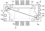
- FIG. 5 is a top layout view of the semiconductor module.
- FIG. 6 is a perspective view of a multilayer wiring bus bar
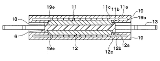
- FIG. 7 is a cross-sectional view of the semiconductor device
- FIG. 8 is an exploded view of the semiconductor device
- FIG. 1 is a circuit diagram of a three-phase inverter circuit configured by a semiconductor module included in the semiconductor device according to the first embodiment of the present disclosure.
- FIG. 2 is a perspective view of the semiconductor module
- FIG. 3 is a perspective view showing a state in which both sides of the semiconductor module are sandwiched between cooling devices
- FIG. 4
- FIG. 9 is a top view of the semiconductor module
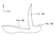
- FIG. 10 is a cross-sectional view of the vicinity of the fin portion
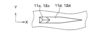
- FIG. 11 is a top view of the fin portion
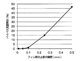
- FIG. 12 is a diagram showing the result of simulating the relationship between the gap at the top of the fin portion and the bypass flow rate ratio
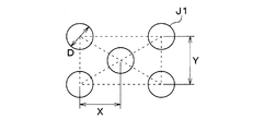
- FIG. 13A is a top surface layout diagram of the model used in the simulation of FIG.
- FIG. 13B is a cross-sectional view of the model used in the simulation of FIG.
- FIG. 14 is a diagram showing the relationship of the deformation amount to the applied load
- FIG. 15A is a cross-sectional view of the model used in the simulation of FIG.
- FIG. 15B is a cross-sectional view of the model used in the simulation of FIG. FIG.
- FIG. 16 is a cross-sectional view of a model of an elliptic arc fin
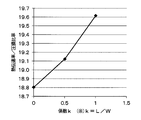
- FIG. 17 is a diagram showing the relationship between the coefficient k and the heat transfer coefficient / pressure loss ratio.
- FIG. 18 is a diagram showing the relationship between the fluid vector and the heat transfer coefficient / pressure loss ratio.
- FIG. 19 is a diagram showing the relationship between the normalized pressure loss and the normalized heat transfer coefficient
- FIG. 20 is a cross-sectional view of a model used for comparison of cooling performance.
- FIG. 21 is a flow velocity contour diagram in the recess
- FIG. 22 is a diagram showing the results of examining the cooling efficiency for each structure when straight fins are used as a reference.
- FIG. 21 is a flow velocity contour diagram in the recess
- FIG. 22 is a diagram showing the results of examining the cooling efficiency for each structure when straight fins are used as a reference.
- FIG. 21 is a flow velocity contour diagram in the recess
- FIG. 22 is a diagram showing the
- FIG. 23 is a diagram showing the relationship between the direction of the refrigerant flow and the direction in which the fins are dug up
- FIG. 24 is a cross-sectional view of the fin portion according to the second embodiment of the present disclosure
- FIG. 25 (a) is a side view of the digging tool
- FIG. 25 (b) is a front view of the digging tool
- FIG.25 (c) is sectional drawing of the fin part dug up by the dug-up tool
- FIG. 26 is a top view of the fin portion according to the third embodiment of the present disclosure
- FIG. 27 is a front view of a digging tool used for forming the fin portion shown in FIG.
- FIG. 28 is a top view of a fin portion according to a modification of the third embodiment
- FIG. 29 is a front view of a digging tool used for forming the fin portion shown in FIG.
- FIG. 30 is a perspective view of a semiconductor device according to the fourth embodiment of the present disclosure.
- FIG. 31 is an exploded view of the semiconductor device shown in FIG.
- FIG. 32 is a cross-sectional view of the fin portions of two semiconductor modules
- FIG. 33 is a perspective view of an inverter unit to which a semiconductor device in which a plurality of semiconductor modules are stacked is applied.
- the configuration of the three-phase inverter circuit 1 provided in the semiconductor module will be described with reference to FIG.
- the three-phase inverter circuit 1 is for driving a load 3 such as a three-phase AC motor based on a DC power source (external power source) 2.
- a smoothing capacitor 4 is connected in parallel to the three-phase inverter circuit 1 so that a constant power supply voltage can be formed by suppressing ripple reduction during switching and the influence of noise.
- the three-phase inverter circuit 1 has a configuration in which upper and lower arms 51 to 56 connected in series are connected in parallel for three phases, and an intermediate potential between the upper arms 51, 53, 55 and the lower arms 52, 54, 56 is applied to the load 3
- the three-phase AC motor to be applied is applied while sequentially switching to the U phase, V phase, and W phase.
- the upper and lower arms 51 to 56 are respectively provided with semiconductor switching elements 51a to 56a such as IGBTs and MOSFETs serving as heating elements and rectifier elements (one-side conduction elements) 51b to 56b for the purpose of reflux such as FWD.
- the semiconductor switching elements 51a to 56a of the upper and lower arms 51 to 56 of each phase are on / off controlled, so that three-phase alternating currents having different cycles are supplied to the three-phase alternating current motor. As a result, the three-phase AC motor can be driven.
- the semiconductor chips on which the semiconductor switching elements 51a to 51f and the rectifying elements 51b to 56b constituting the six upper and lower arms 51 to 56 provided in the three-phase inverter circuit 1 are formed as a module and integrated.
- the three-phase inverter circuit 1 is configured as a 6-in-1 semiconductor module in which six arms are integrated.
- the semiconductor module 6 shown in FIG. 2 includes a semiconductor chip 10, upper and lower radiator plates 11, 12, a multilayer wiring bus bar 13 in which various terminals and wires are integrated, a control terminal 14, and an element relay electrode. 15 and plates 16, 17 and the like. Of these, six sets of component blocks are provided, with the semiconductor chip 10, the control terminal 14, the element relay electrode 15, the plates 16, 17, etc. as component blocks for one arm. Then, six sets of component parts blocks are sandwiched between the upper and lower radiator plates 11 and 12 together with the multilayer wiring bus bar 13 and covered with a resin mold portion 18 as shown in FIG. Thus, the semiconductor module 6 is configured as a plate-like member having a predetermined thickness as shown in FIG.
- Such a semiconductor module 6 is used to drive the load 3 while dissipating heat by sandwiching both sides in the thickness direction by a cooler 19 as shown in FIG.
- a cooler 19 as shown in FIG.
- through holes 19a are provided at two opposite corners of each cooler 19, and a passage constituting portion 19d that constitutes a refrigerant passage by connecting each through hole 10a is provided. Thereby, the cooling of the cooler 19 is performed, so that the semiconductor module 6 is used while enabling efficient cooling.
- the semiconductor chip 10 shown in FIG. 4 is composed of six chips 10a to 10f.
- Each of the chips 10a to 10f has a front surface and a back surface, and semiconductor switching elements 51a to 56a, rectifying elements 51b to 56b, and the like constituting the upper arms 51, 53, 55 or the lower arms 52, 54, 56, respectively, are formed.
- the semiconductor chip 10 is formed using a semiconductor substrate such as Si, SiC, or GaN as a base material substrate.
- the semiconductor switching elements 51a to 56a and the rectifying elements 51b to 56b formed in the semiconductor chip 10 are vertical elements that allow current to flow in the direction perpendicular to the substrate, and various electrodes are provided on the front and back sides of the semiconductor chip 10.
- each semiconductor chip 10 is electrically and physically connected to the surface side of the lower plate 17 via a bonding material 20 made of a high thermal conductive material such as solder or Ag sintered material. It is connected to the. And the back surface side of the lower plate 17 is joined to the lower heat radiating plate 12 via a joining material 21 made of a high thermal conductive material such as solder or Ag sintered material.
- the surface side of the semiconductor chip 10 is a bonding material 22 made of a high thermal conductive material such as solder or Ag sintered material with respect to the element relay electrode 15 made of Cu, Al, Fe or the like as a base material. Connected through. Furthermore, the element relay electrode 15 is electrically and physically connected to the back surface side of the upper plate 16 through a bonding material 23 made of a high thermal conductive material such as solder or Ag sintered material. And the surface side of the upper side plate 16 is joined to the upper side heat sink 11 via the joining material 24 comprised with the high heat conductive material like a solder or Ag sintered material.
- each semiconductor chip 10 is sandwiched between the upper and lower radiator plates 11 and 12.
- the semiconductor chip 10 is configured such that elements such as the semiconductor switching elements 51a to 56a and the rectifying elements 51b to 56b constituting the arms 51 to 56 are formed together in one chip.
- elements such as semiconductor switching elements 51a to 56a and rectifying elements 51b to 56b constituting the arms 51 to 56 may be formed on separate chips.
- the upper and lower heat sinks 11 and 12 correspond to heat sinks, and are composed of, for example, a high thermal conductive member mainly composed of Cu, Al, Fe, etc., one surface side facing the semiconductor chip 10 and the other surface side shown in FIG. 2, the resin mold portion 18 is exposed.
- the upper and lower heat radiating plates 11 and 12 are stepped, and the inner side portions 11b and 12b (see FIG. 7) that are inside the outer edge portions 11a and 12a (see FIG. 7). Is projected by a predetermined amount.
- the outer edge portions 11 a and 12 a are flush with one surface of the resin mold portion 18 around the outer edge portions 11 a and 12 a, and the inner portions 11 b and 12 b protrude from the resin mold portion 18 by a predetermined distance.
- the inner portions 11b and 12b are formed with a plurality of fin portions 11c and 12c formed by digging up the surface layer portions of the inner portions 11b and 12b and using a tool. The detailed structure of the plurality of fin portions 11c and 12c will be described later. In FIG. 7, each component provided in the resin mold portion 18 is omitted from illustration.
- the upper and lower radiator plates 11 and 12 are in an insulated state from the semiconductor chip 10 because the upper and lower plates 16 and 17 are partially made of an insulating material.
- the upper and lower plates 16 and 17 and the element relay electrode 15 are made of a highly heat conductive material, the upper and lower heat sinks 11 and 12 have high heat conduction from the semiconductor chip 10. It is reported in. Then, heat can be radiated from the front surface side of the upper heat radiating plate 11 and the back surface side of the lower heat radiating plate 12, that is, the surface on which the fin portions 11c and 12c are formed.
- the multilayer wiring bus bar 13 is a part constituting various wirings and various terminals in the semiconductor module 6 of the present embodiment.
- the multilayer wiring bus bar 13 is composed of a plate-like bar-like member, and includes the semiconductor chip 10 that constitutes the upper arms 51, 53, and 55 of each phase and the semiconductor chip 10 that constitutes the lower arms 52, 54, and 56. It is arranged to pass between.
- the positive side wiring connecting the upper arms 51, 53, 55 and the + terminal of the DC power source 2 and the negative electrode connecting the lower arms 52, 54, 56 and the ⁇ terminal of the DC power source 2.
- Side wiring and output wiring for connecting the arms 51 to 56 and the load 3 are provided.
- the multilayer wiring bus bar 13 is provided with various connection terminals 13a to 13e for connecting each wiring to the DC power source 2 and the load 3.
- the multilayer wiring bus bar 13 is configured by a plate-like bar-shaped member having one direction as a longitudinal direction, and one end side and the other end side are substantially square as shown in FIG. 2. It is exposed from the two opposite sides of the resin mold part 18 having a shape.
- the positive terminal 13 a that connects the upper arms 51, 53, 55 and the positive terminal of the DC power source 2, the lower arms 52, 54, 56 and the DC power source 2
- a negative terminal 13b is formed to connect the negative terminal.
- a U terminal 13c corresponding to an output terminal for connecting the intermediate potential point of the upper and lower arms 51 to 56 and the load 3 in each phase of the U phase, V phase, and W phase.
- a V terminal 13d and a W terminal 13e are exposed from the resin mold 18 as shown in FIG.
- the semiconductor module 6 and the DC power source 2 and the smoothing capacitor 4 are electrically connected via the positive terminal 13a and the negative terminal 13b.
- electrical connection with the U-phase, V-phase, and W-phase of the three-phase AC motor serving as the load 3 is performed via the U terminal 13c, the V terminal 13d, and the W terminal 13e.
- Such a multilayer wiring bus bar 13 is configured by a multilayer wiring structure in which patterned conductor layers and insulating layers are laminated, and circuit wiring for electrically connecting each part of the three-phase inverter circuit 1 shown in FIG. Is configured.
- the pads 136a to 136c and 139a to 139c provided in the multilayer wiring bus bar 13 are electrically connected to predetermined portions of the semiconductor chips 10a to 10f.
- a plurality of pads electrically connected to predetermined portions of the semiconductor chips 10a to 10f are also provided on the surface of the multilayer wiring bus bar 13 opposite to the surface on which the pads 136a to 136c and 139a to 139c are disposed. Is provided.
- the internal wiring provided in the multilayer wiring bus bar 13 and the pads 136a to 136c, 139a to 139c are electrically connected, and the internal wiring and the terminals 13a to 13e are electrically connected to each other, so that the three-phase inverter
- the wiring structure of the circuit 1 is configured.
- the internal wiring is covered with an insulating film 130, and pads 136a to 136c, 139a to 139c and terminals 13a to 13e are provided so as to be exposed from the insulating film 130.
- the control terminal 14 serves as a signal line terminal constituting various signal lines such as gate wirings of the semiconductor switching elements 51a to 56a.
- the control terminal 14 is electrically connected to the electrodes connected to the gates of the semiconductor switching elements 51a to 56a formed on the surface side of the semiconductor chip 10 via bonding wires 25 (see FIG. 4) made of Au or the like. It is connected to the.
- the end portion of the control terminal 14 opposite to the semiconductor chip 10 is exposed from the resin mold portion 18 as shown in FIG. 2, and is configured to be connected to the outside through this exposed portion.
- the control terminal 14 is described as being integrated in a lead frame state, and is also integrated with the lower heat sink 12.
- the signal lines are divided, and each signal line becomes independent.
- the element relay electrode 15 is a member that is electrically connected to the upper plate 16 while being electrically connected to the electrode on the surface of the semiconductor chip 10 on one surface of the semiconductor chip 10 side.
- the element relay electrode 15 is provided in order to provide a gap between the semiconductor chip 10 and the upper plate 16 by an amount corresponding to the bonding wire 25 disposed.
- the element relay electrode 15 is composed of a high heat conductive member mainly composed of Cu or the like, for example.
- the upper plate 16 serves to insulate the semiconductor chip 10 and the upper heat dissipation plate 11 from each other on the one surface of the semiconductor chip 10 while electrically connecting to the surface electrode of the semiconductor chip 10 via the element relay electrode 15. Fulfill.
- the lower plate 17 serves to insulate the semiconductor chip 10 and the lower heat dissipation plate 12 while making electrical connection with the electrode on the back surface of the semiconductor chip 10 on one surface of the semiconductor chip 10 side.
- the upper and lower plates 16 and 17 on the side of the semiconductor chip 10 is constituted by a high heat conductive member whose base material is Cu, Al or the like so that thermal conductivity is enhanced in addition to electrical connection.
- the layer located on the opposite side of the semiconductor chip 10 side from the one surface on the semiconductor chip 10 side is made of, for example, inorganic or organic so as to increase the thermal conductivity while achieving insulation. It is made of an insulating material.
- the upper and lower plates 16 and 17 can be configured by bonding a conductive plate having Cu as a base material on both surfaces of a ceramic insulator such as Si 3 N 4 , AlN, or Al 2 O 3 .
- the upper and lower plates 16 and 17 may be configured by bonding a Cu plate having an insulating sheet attached thereto and an adhesive sheet having an insulating adhesion function to a die bond plate made of a conductor member such as Cu. it can.
- the upper plate 16 has the surface electrodes of the semiconductor switching elements 51a to 56a (for example, the source of the MOSFET and the emitter of the IGBT) and the first electrodes of the rectifying elements 51b to 56b (for example, the anode such as FWD). ).
- the upper plate 16 is also electrically connected to the pads 136a to 136c and 139a to 139c provided on the multilayer wiring bus bar 13.
- the lower plate 17 is connected to the back electrodes of the semiconductor switching elements 51a to 56a (for example, the drain of the MOSFET and the collector of the IGBT) and the second electrodes of the rectifying elements 51b to 56b (for example, the cathode such as FWD).
- the lower plate 17 is also electrically connected to each pad (not shown) provided on the back side of the multilayer wiring bus bar 13. For this reason, the upper and lower plates 16 and 17 constitute part of the positive electrode side wiring, the negative electrode side wiring, and the output wiring for each of the arms 51 to 56.
- both the surface side of the upper heat radiating plate 11 and the back surface side of the lower heat radiating plate 12, that is, the surface opposite to the surface on which the semiconductor chip 10 is disposed are both from the resin mold portion 18. It is exposed, and heat can be radiated in this exposed portion.
- a cooler 19 is disposed on the heat radiation surface side. As shown in FIG. 7, the cooler 19 has a flow passage 19b formed by a cavity formed therein, and the refrigerant can flow through the flow passage 19b. For this reason, the heat radiating surfaces of the upper and lower heat radiating plates 11 and 12 come into contact with the refrigerant.
- the insulation between the semiconductor chip 10 and the upper and lower heat sinks 11 and 12 is achieved by the upper and lower plates 16 and 17, the current flows to the outside through the upper and lower heat sinks 11 and 12. Leakage can be prevented from occurring.
- the resin mold portion 18 is a sealing resin configured by placing each of the above-described components in a mold and then encapsulating the resin in the mold, and is configured, for example, in a rectangular plate shape.
- the resin mold part 18 is made of an insulating resin having a lower linear expansion coefficient and Young's modulus than the conductor parts such as the upper and lower radiator plates 11 and 12.
- the resin mold portion 18 can be mainly composed of an organic resin such as epoxy or silicone. From the resin mold portion 18, the front end of the control terminal 14 and both ends of the multilayer wiring bus bar 13 are exposed from each side constituting the quadrangular plate shape, and can be electrically connected to the outside.
- control terminals 14 of the upper arms 51, 53, and 55 and the lower arm 52 from opposite two sides of the resin mold portion 18 that is formed in a rectangular plate shape, that is, in the opposite direction across the resin mold portion 18,
- the control terminals 14 of 54 and 56 are exposed.
- both ends of the multilayer wiring bus bar 13 are exposed from two opposite sides of the resin mold portion 18 having a rectangular plate shape, that is, in opposite directions across the resin mold portion 18.
- the upper heat radiating plate 11 and the lower heat radiating plate 12 are exposed from the front and back surfaces of the rectangular plate shape, respectively, so that heat can be radiated satisfactorily.
- the above-described parts are mounted on the surface side of the lower heat sink 12 in the lead frame state in which the control terminals 14 are integrated. Then, after the electrical connection between the semiconductor chip 10 and the control terminal 14 is completed with the bonding wires 25, the upper heat radiating plate 11 and the like are mounted thereon. In this state, these are placed in a mold, and a resin mold portion 18 is formed by injecting resin into the mold and molding it. In addition to the surfaces of the upper and lower heat sinks 11 and 12, the resin mold portion 18 covers other than the exposed portions of the control terminal 14 and the multilayer wiring bus bar 13, thereby protecting the semiconductor chip 10 and the like.
- the cooler 19 includes a refrigerant passage 19b therein, and promotes heat dissipation of the semiconductor module 6 by allowing the refrigerant to flow.
- the cooler 19 is disposed on both heat radiation surfaces of the semiconductor module 6 where the upper and lower heat sinks 11 and 12 are disposed, and the cooler 19 and the semiconductor module 6 are stacked so as to sandwich the semiconductor module 6 by the cooler 19. ing. Then, as shown in FIG. 8, the cooler 19 and the semiconductor module 6 are fastened with bolts 28 while the semiconductor module 6 is sandwiched between the two coolers 19.
- the cooler 19 includes a hollow plate-like portion 19c having a substantially rectangular shape when viewed from the side opposite to the semiconductor module 6 and a passage constituting portion in which a through hole 19a is formed. 19d.
- the hollow portion configured in the hollow plate-like portion 19c as the refrigerant passage 10b With the hollow portion configured in the hollow plate-like portion 19c as the refrigerant passage 10b, the refrigerant introduced from one through hole 19a passes through the refrigerant passage 19b and is then discharged from the other through hole 19a.
- an opening 19e connected to the refrigerant passage 19b is formed on one surface of the hollow plate-like portion 19c on the semiconductor module 6 side.
- Inner portions 11b and 12b and fin portions 11c and 12c are arranged in the opening 19e.
- the outer edge shape of the inner side portions 11b and 12b and the shape of the opening portion 19e are matched, and the cooler 19 is assembled to the semiconductor module 6 so that the inner side portions 11b and 12b are fitted into the opening portion 19e.
- One surface of the hollow plate-like portion 19c on the side of the semiconductor module 6 has a structure having a predetermined thickness, and the thickness is made to match the protruding amount from the outer edge portions 11a and 12a of the inner portions 11b and 12b. .
- a seal member 26 surrounding the opening 19 e is disposed between the cooler 19 and the semiconductor module 6. For this reason, the space between the cooler 19 and the semiconductor module 6 is sealed by the sealing member 26 to prevent refrigerant leakage.
- the dimension of the refrigerant passage 19b formed in the cooler 19 is smaller than the height of the fin portions 11c and 12c.
- the tips of the fin portions 11c and 12c are tapered to facilitate deformation. For this reason, when the semiconductor module 6 and the cooler 19 are assembled, the fin portions 11c and 12c are brought into contact with the inner wall surfaces of the cooler 19 constituting the refrigerant passage 19b and the tips of the fin portions 11c and 12c are in contact with each other. When contacted, the tips of the fin portions 11c and 12c are deformed. As a result, the seal portion 26 is disposed without a gap between the cooler 19 and the semiconductor module 6 so that the seal function can be exhibited accurately.
- the passage constituting portion 19d has a rectangular shape, and a through hole 19a is formed at the center position thereof.
- the passage constituting portions 19d of the adjacent coolers 19 are in close contact with each other via a seal member 27 surrounding the through hole 19a, and the through holes 19a are connected to each other.
- the through hole 19a communicates with the refrigerant passage 19b. For this reason, the refrigerant introduced from the through hole 19a of one passage component 19d brought into close contact with each other passes through the refrigerant passage 10b and discharged from the through hole 19a of the other passage component 19d brought into close contact with each other. Is done.
- the dimension of the refrigerant passage 19b formed in the cooler 19 is smaller than the height of the fin portions 11c and 12c.
- the tip position of 12c is easily deformed.
- sticker part 26 is arrange
- path structure part 19d are arrange
- the end of the multilayer wiring bus bar 13 on the side where the positive and negative terminals 13a and 13b are arranged and the end on the side where the U to W terminals 13c to 13e are arranged are substantially rectangular. It arrange
- FIG. A through hole 19a is disposed at a position shifted from each of the terminals 13a to 13e. Therefore, the terminals 13a to 13e can be electrically connected to the external wiring without being hidden by the through hole 19a and the passage component 19d in the cooler 19.
- a semiconductor device having the semiconductor module 6 according to the present embodiment is configured by the structure as described above. Next, the detailed structure of the plurality of fin portions 11c and 12c formed on the heat radiating plates 11 and 12 will be described with reference to FIGS. 2, 7 and 9 to 11. FIG. In addition, although the several fin part 11c is mainly demonstrated here, the several fin part 12c is also set as the structure similar to the several fin part 11c.
- the inner portion 11b has a rectangular shape having a long side in the same direction as the longitudinal direction of the multilayer wiring bus bar 13 and a short side in the direction perpendicular thereto.
- the long side direction of the inner portion 11b is the x direction
- the short side direction is the y direction
- the normal direction of the inner portion 11b is the z direction
- the plurality of fin portions 11c are in the x direction and the y direction.
- each one of the several fin part 11c is comprised by digging up the surface of the inner side part 11b, and digging up in the z-axis direction with a tool.
- a plurality of rows arranged at equal intervals in the y direction are arranged at equal intervals in the x direction.
- column is shifted, and the layout which each fin part 11c of each row
- the refrigerant flow direction in the cooler 19 is a direction from the through hole 19a on the refrigerant introduction side to the through hole 19a on the refrigerant discharge side, and is indicated by an arrow A1 in the figure.
- the plurality of fin portions 11c arranged in a staggered arrangement are arranged along the refrigerant flow direction.
- the plurality of fin portions 11c being arranged along the refrigerant flow direction may mean that the plurality of fin portions 11c do not have to be parallel to the refrigerant flow direction, and the arrangement direction and the refrigerant flow direction. And may be angled.
- the plurality of fin portions 11c are formed by digging up the surface of the inner portion 11b along the y direction. For this reason, the coolant flow direction (arrow A1 in the figure) forms an acute angle in the range of greater than 0 ° and 45 ° or less with respect to the direction in which the plurality of fin portions 11c are raised (arrow B1 in the figure).
- Each of the plurality of fin portions 11c has an elliptical arc shape that is curved from the root portion to the tip portion. More specifically, as shown in FIG. 10, each fin portion 11 c has an elliptical arc-shaped cross section cut into a plane parallel to the digging direction and parallel to the normal direction to the surface of the inner portion 11 b. And each fin part 11c is made into the structure which deform
- the width of digging up the inner portion 11b is set to a constant width, and as shown in FIG. 10, the digging depth is gradually increased while the depth is fixed from the middle position of the digging up. It is said. Accordingly, each fin portion 11c has a constant thickness in the same direction as the digging direction from the root to the middle position of the digging, and the thickness gradually decreases from the middle position to the tip.
- each fin part 11c has a structure which receives the flow rate of a refrigerant
- each fin portion 11c is arbitrary, but in order to suppress the deterioration of the refrigerant flow and the induction of complicated turbulence caused by the recess 11d formed after digging as will be described later, the thickness and y in the x direction are suppressed.
- the width that becomes the dimension in the direction is 1 mm or less, and the height that becomes the dimension in the z direction is less than 10 mm.
- the height of the fin portion 11 c is larger than the dimension of the refrigerant passage 19 b formed in the cooler 19 in the stacking direction of the semiconductor module 6 and the cooler 19.
- the height of the fin portion 11c is preferably set so that the difference between the height of the fin portion 11c and the dimension of the refrigerant passage 19b is smaller than the maximum deformation amount of the fin portion 11c.
- a plurality of fin portions 11c, 12c formed on the upper and lower radiator plates 11, 12 are formed by digging up the surfaces of the upper and lower radiator plates 11, 12. Yes. For this reason, before digging up the plurality of fin portions 11c and 12c, the surfaces of the upper and lower heat sinks 11 and 12 are flat, and the bonding state of the internal element portions is inspected by an ultrasonic imaging apparatus or the like. It becomes possible to do.
- the thickness of one surface of the hollow plate-like portion 19c in the cooler 19 on the semiconductor module 6 side and the protruding amount of the inner portions 11b and 12b are matched.
- the fin portions 11c and 12c are exposed to a place where the refrigerant easily flows in the refrigerant flow passage 19b in the entire height.
- the inner portions 11b and 12b may be flush with the outer edge portions 11a and 12a and the resin mold portion 18, but in that case, the root portions of the fin portions 11c and 12c are hidden in the recesses formed by the thickness of the cooler 19, The root portion is located in the refrigerant passage 19b where the refrigerant does not flow easily.
- the root portions of the fin portions 11c and 12c are not hidden by the thickness of the cooler 19, and the root portions It can be located in a place where the refrigerant can easily flow. Therefore, the heat dissipation efficiency can be increased, and as a result, the height of the fin portions 11c and 12c can be reduced, and the semiconductor device can be reduced in size.
- the dimension of the refrigerant passage 19b formed in the cooler 19 is smaller than the height of the fin portions 11c and 12c. For this reason, the front-end
- bypass flow rate the relationship between the width of the upper portion of the fin portion, that is, the width of the bypass passage and the flow rate flowing through the bypass passage (hereinafter referred to as bypass flow rate) was examined by simulation.
- FIG. 12 shows the result.
- a gap J3 between the straight fins J1 and the cooler J2 is changed using a simulation model in which a plurality of straight fins J1 are arranged in a staggered arrangement.
- the bypass flow rate was examined.
- the diameter of the straight fin J1 is D
- the height hc is 2 ⁇ D
- the pitch in the x direction between adjacent rows of the straight fins J1 is 2 ⁇ D
- the pitch in the y direction between the same rows was also 2 ⁇ D.
- coolant was assumed.
- the ratio of the bypass flow rate is as low as about 0 to 2%. At 15%. The ratio of the bypass flow rate increased as the gap J3 increased.
- the gap J3 exceeds 0.1 mm, the ratio of the bypass flow rate is significantly increased.
- the cylindrical portion in which a plurality of straight fins are formed is inserted into the cooling base, it is manufactured so that the cylindrical portion in which the plurality of straight fins are formed can be accurately inserted into the cooling base. It is necessary to set the height of the straight fins taking into account tolerances and warping of the fins. For this reason, the clearance gap between the front-end
- the tips of the fin portions 11c and 12c are in contact with the inner wall surface of the hollow plate-like portion 19c in the cooler 19 so that no gap is left between them. Therefore, it is possible to prevent a bypass passage from being formed between the tips of the fin portions 11c and 12c and the hollow plate-like portion 19c, and it is possible to suppress a decrease in heat dissipation efficiency.
- the tips of the fin portions 11c and 12c are tapered. For this reason, the fin parts 11c and 12c can be easily deformed in the height direction. Therefore, in the stacking direction of the semiconductor module 6 and the cooler 19, even if the dimension of the refrigerant passage 19b formed in the cooler 19 is smaller than the height of the fin portions 11c and 12c, due to the deformation of the fin portions 11c and 12c, The dimensional difference can be absorbed.
- the fin portion 11c is sized to the size of the refrigerant passage 19b formed in the cooler 19 in the stacking direction of the semiconductor module 6 and the cooler 19. , 12c may be brought close to each other. If the gap at this time is set to 0.1 mm or less, the ratio of the bypass flow rate can be reduced, so that a decrease in cooling efficiency can be suppressed.
- the dimension of the refrigerant passage 19b formed in the cooler 19 in the stacking direction of the semiconductor module 6 and the cooler 19 is the same as that of the fin portions 11c and 12c.
- the height is preferably smaller than the height.
- FIG. 14 is a diagram showing the evaluation results.
- SH-L in FIG. 14 uses an evaluation model in which the fin portions 11c and 12c are tapered as in this embodiment.
- FH-L in FIG. 14 uses an evaluation model in which the fin portions 11c and 12c have a constant diameter from the root to the tip as in the case of the straight fin.
- the amount of deformation was examined by changing the thickness at 2, 0.4 mm.
- the amount of deformation is large even with a low load.
- it becomes possible to obtain a desired amount of deformation with a low load by making the fin portions 11c, 12c into an elliptical arc shape with tapered tips. This is because the fin portions 11c and 12c are tapered elliptical arcs.
- the taper shape having a small cross-sectional area facilitates deformation
- the elliptical arc shape increases the amount of deformation in the z direction.
- the protruding amount L increases, the deformation region shifts to the tip portion, so that deformation in the z direction can be generated even with a lower load.
- the distortion of the fin portions 11c and 12c when the deformation is 0.1 mm which is the target value of the deformation, is calculated to be sufficiently smaller than 0.2%. It was confirmed. In the case of such a strain, the deformation of the fin portions 11c and 12c is a deformation in the elastic deformation region. Therefore, damage to the fin portions 11c and 12c can be suppressed.
- the digging direction and the refrigerant flow direction form an acute angle while the plurality of fin portions 11c and 12c are formed in an elliptical arc shape. Since it is set as such a structure, it becomes possible to improve the cooling performance by the several fin parts 11c and 12c, and it becomes possible to improve heat dissipation efficiency.
- heat transfer coefficient and pressure loss are indicators of cooling performance, depending on the shape of the fin part and how the refrigerant hits the fin part, even if the refrigerant path is determined Is different.
- a high heat transfer rate / pressure loss ratio can be said to be a cooler with high cooling performance.
- thermal fluid analysis was performed on a model in which elliptical arc-shaped fins were arranged in a staggered arrangement.
- the protrusion amount L is based on the digging width W (corresponding to the width of the fin portion) corresponding to the digging depth.
- L 0, 0.5 ⁇ W, and 1.0 ⁇ W.
- the simulation was performed with the side positioned on the downstream side.
- k L / W
- the heat transfer rate / pressure loss ratio is high, and the digging direction is given a certain angle with respect to the x direction.
- the heat transfer coefficient / pressure loss ratio is further increased.
- the case where the fluid vector ⁇ is 135 to 225 ° means that the refrigerant flow direction is in the range of 0 to 45 ° with respect to the digging direction.
- the coolant flow direction is an acute angle in the range of greater than 0 ° and less than or equal to 45 ° with respect to the digging direction
- the heat transfer coefficient / pressure loss ratio increases when the coolant flow direction becomes an acute angle in the range of greater than 0 ° and less than 30 ° (the range of 150 ° to less than 180 ° in terms of fluid vector ⁇ ) with respect to the digging direction. Therefore, it can be said that these ranges have the highest cooling efficiency.
- the cooling performance by the plurality of fin portions 11c and 12c can be improved by making the digging direction and the coolant flow direction form an acute angle while making the plurality of fin portions 11c and 12c have an elliptical arc shape, and more heat dissipation efficiency. Can be improved.
- the recesses 11d and 12d are arranged on the downstream side of the refrigerant flow with respect to the fin portions 11c and 12c. For this reason, the influence which the recessed parts 11d and 12d have on a refrigerant
- coolant flow can be suppressed, and the improvement of cooling performance can be aimed at more.
- the fin portions 11c and 12c are used as simple straight pins, and there are no recesses 11d and 12d as shown by a broken line when there are recesses 11d and 12d as shown by a solid line.
- the cooling performance (heat transfer coefficient and pressure loss) was compared.
- the concave portions 11d and 12d are downstream of the refrigerant flow with respect to the fin portions 11c and 12c. It is arranged on the side, that is, on the back side of the flow velocity. Since the flow rate inevitably decreases in the vicinity of the back surfaces of the fin portions 11c and 12c when viewed from the flow rate, the influence can be reduced by bringing the recesses 11d and 12d to the back side where the flow rate decreases.
- the refrigerant flow in the z direction is also induced.
- the refrigerant flows in and the area in the recess is also used as a heat transfer surface. For this reason, it is effective for suppressing the influence by forming the recessed parts 11d and 12d.
- the convex surfaces of the fin portions 11c and 12c having an elliptical arc shape are positioned on the upstream side of the refrigerant flow, the refrigerant hits the mid-portion of the fin portions 11c and 12c and is in the z direction. Easy to induce flow to For this reason, the said effect can be acquired more.
- the fin portions 11c and 12c are formed in an elliptical arc shape while the fin portions 11c and 12c are formed by digging up. For this reason, the flow of the refrigerant
- the surface can be made flat before the fin portions 11c and 12c are dug up, and a semiconductor device capable of cooling the semiconductor module 6 with higher cooling efficiency can be obtained.
- the concave portions 11d and 12d are arranged on the downstream side of the refrigerant flow with respect to the fin portions 11c and 12c. Further, the fin portions 11c and 12c are formed in an elliptical arc shape, and the convex surface side is arranged on the upstream side of the refrigerant flow with respect to the concave surface side. The direction in which the fins 11c and 12c are dug up and the direction of the refrigerant flow form an acute angle. With these configurations, a semiconductor device capable of cooling the semiconductor module 6 with higher cooling efficiency can be obtained.
- the recesses 11d and 12d have the highest influence due to the positional relationship, and it is preferable to form the recesses 11d and 12d on the back side of the flow velocity with respect to the fin portions 11c and 12c.
- the fin portions 11c and 12c have an elliptical arc shape, comparing the case where the convex surface side is directed to the upstream side of the refrigerant flow and the case where the concave surface side is directed, the direction where the convex surface side is directed is 2 in the z direction. As a result, it was easy to induce the next flow, and the heat dissipation performance was improved, which was preferable.
- the digging direction of the fin portions 11c and 12c when the flow velocity vector ⁇ is set within a predetermined angle range so that the digging direction and the refrigerant flow direction form an acute angle (for example, 30 °), the digging direction and the refrigerant flow The heat dissipation performance was higher than when matching the direction.
- the fin portions 11c and 12c are elliptical arcs, either the case where the convex surface side is directed to the upstream side of the refrigerant flow or the case where the concave surface side is directed As for, the heat dissipation performance became higher.
- the fin portion after digging up so that the direction in which the convex surfaces of the fin portions 11c, 12c are directed forms an acute angle with respect to the refrigerant flow direction while the digging direction (x direction in the figure) of the fin portions 11c, 12c is directed to the refrigerant flow direction.
- 11c and 12c can be processed, processing is difficult.
- the substantially rectangular surface in which the through holes 19a on each of the refrigerant introduction side and the discharge side are provided with a plurality of fin portions 11c and 12c. And it is made to be located in the diagonal of the back surface heat sinks 11 and 12.
- the straight line connecting the centers of the through holes 19a and the x direction form an acute angle ⁇ greater than 0 ° and 45 ° or less while matching the direction in which the fins 11c and 12c are raised and the direction in which the convex surface is directed. I am doing so. Accordingly, the direction in which the fin portions 11c and 12c are dug up, that is, the direction in which the convex surface is directed and the direction of the refrigerant flow can be made to form an angle ⁇ .
- the fin portions 11c and 12c are formed in an elliptical arc shape by digging up the surfaces of the inner portions 11b and 12b, but the convex surface side of the fin portions 11c and 12c is the downstream side of the refrigerant flow, the concave surface The side is directed upstream of the refrigerant flow.
- the shape after digging is likely to be the shape as in this embodiment. For this reason, it is possible to easily process the fin portions 11c and 12c having the structure of the present embodiment.
- processing is difficult compared to the structure of this embodiment, such as performing shape processing of the fin portions 11c and 12c after digging up. Therefore, it is possible to simplify the manufacturing process when manufacturing the semiconductor device having the structure of the present embodiment.
- the fin portions 11c and 12c are digged up using the digging tool 100 having the cutting edge 100a.
- the cutting edge 100a is L-shaped bent in the vertical direction from the base 100b, and the tip is linear.
- the surface of the inner parts 11b and 12b is digged up so that the depth is constant from the middle position of the digging up while gradually raising the digging depth.
- the concave portions 11d and 12d are formed, the convex surface side faces away from the concave portions 11d and 12d, and the concave surface side faces the concave portions 11d and 12d. Can be formed.
- the surface of the fins 11c and 12c that has been dug is not a flat surface, but a curved surface that protrudes toward the recesses 11d and 12d.
- the recesses 11d and 12d are factors that affect the refrigerant flow. However, the smaller the volume in the recesses 11d and 12d, the less influence the refrigerant flow has. In addition, the shape of the fin portions 11c and 12c is advantageous when the pressure loss is taken into consideration.
- the cross-sectional shape of the fin portions 11c and 12c is a rectangular shape, and the cross-sectional shape of the concave portion is also a rectangular shape.
- the surface of the fin portions 11c and 12c that has been dug up is a curved surface, specifically an elliptical arc surface.
- the volumes in the recesses 11d and 12d are also the same as those in the first and second embodiments. Less than the structure. Therefore, it is possible to suppress the influence of the recesses 11d and 12d on the refrigerant flow, and further improve the cooling performance.
- Such a structure can be processed by changing the tip shape of the cutting edge 100a of the digging tool 100 as shown in FIG. That is, if the cutting edge 100a is semi-elliptical arc, the cross-sectional shape of the digging surface of the fin portions 11c and 12c formed by digging can be an elliptical arc-shaped curved surface.
- the cross-sectional shape of the fin parts 11c and 12c was made into the elliptical arc-shaped curved surface as an example which made the tapering shape the surface side which digged up among the fin parts 11c and 12c.
- Other tapered shapes for example, as shown in FIG. 28, the surface of the fin portions 11c and 12c that have been dug up may be a V-shaped surface. Even if it does in this way, the effect similar to 3rd Embodiment can be acquired.
- Such a structure can be processed by making the tip shape of the cutting edge 100a of the digging tool 100 V-shaped as shown in FIG.
- two semiconductor modules 6 are provided, and two semiconductor modules 6 are arranged between three coolers 19. Specifically, one semiconductor module 6 is disposed on both sides of one cooler 19, and one cooler 19 is disposed on both sides so as to sandwich two semiconductor modules 6 and one cooler 19. The structure is arranged.
- the cooler 19 sandwiched between the two semiconductor modules 6 has openings 19e on both sides of the front and back surfaces.
- the inner portion 11b and the fin portion 11c of the upper radiator plate 11 of one semiconductor module 6 are inserted into one opening portion 19e, and the lower radiator plate 12 of the other semiconductor module 6 is inserted into the other opening portion 19e.
- the inner part 12b and the fin part 12c are inserted.
- the dimension hc of the flow passage 19b formed in the cooler 19 in the height direction of the fin portions 11c and 12c is made smaller than the sum of the heights 2 ⁇ dc of both the fin portions 11c and 12c. Yes. By doing in this way, it can prevent that a clearance gap is formed between both the front-end
- a semiconductor device in which a plurality of semiconductor modules 6 are stacked in this way is applied to an inverter unit as shown in FIG. 33, for example.
- the inverter unit shown in FIG. 33 has a substantially rectangular parallelepiped shape, and on one surface side, a pipe member 200 connected to the passage component 19b in the stacking direction of the semiconductor module 6 and the cooler 19 is provided.
- a nut portion 201 is provided at the tip of the pipe member 200, and the nut portion 201 is connected to another pipe member (not shown) to introduce and discharge the refrigerant.
- one end side of the multilayer wiring bus bar 13 protrudes from one surface having one direction orthogonal to the stacking direction of the semiconductor modules 6 and the cooler 19 as a normal direction, and the other end side of the multilayer wiring bus bar 13 extends from the surface opposite to the one surface. It sticks out.
- a positive electrode terminal 202a and a negative electrode terminal 202b are connected to the positive electrode and negative electrode terminals 13a and 13b arranged on one end side of the multilayer wiring bus bar 13, and a positive electrode and a negative electrode of a power source (not shown) are connected to each of these terminals 202a and 202b. Supply is made.
- U, V and W terminals 202c to 202e are connected to U to W terminals 13c to 13e arranged on the other end side of the multilayer wiring bus bar 13. These terminals 202c to 202e are connected to U to W terminals of a motor (not shown) driven by an inverter unit to supply current corresponding to each phase.
- the two semiconductor modules 6 can be driven in parallel or different motors.
- the two motors can be driven by connecting to the U to W terminals. In that case, if the positive and negative terminals 13a, 13b of the two semiconductor modules 6 are connected to different power sources, the two motors can be driven by different voltages.
- the inverter unit has an outer frame portion configured by columnar stays 204 arranged at four corners and a support member 205 that extends in the stacking direction of the semiconductor modules 6 and connects the two stays 204. Surrounded.
- a printed circuit board 206 provided with a control circuit is fixed to both ends of each stay 204 in the outer frame portion by screws or the like.
- the control terminal 14 is inserted into a through hole formed in the printed board 206 and soldered, whereby the control terminal 14 and the control circuit are electrically connected.
- the capacitor module 207 which comprises the smoothing capacitor 4 is being fixed to the surface of the cooler 19 in the one surface side in which the pipe member 200 was provided.
- the capacitor module 207 is a ceramic capacitor made of, for example, barium titanate having a high dielectric constant, and is a plate-like member.
- the capacitor module 207 may be constituted by a film capacitor such as PP material, but by using a small and large-capacity ceramic capacitor, a small space where the cooler 19 is disposed can be effectively used.
- the capacitor module 207 can be mounted. As a result, the inverter unit can be miniaturized.
- FIG. 1 a structure having a plurality of semiconductor modules 6 can be provided.
- an inverter unit can also be comprised by the structure provided with several such semiconductor modules 6.
- the tip is tapered, and the digging direction and the direction of the refrigerant flow form an acute angle.
- the semiconductor switching elements 51a to 56a have been described as examples of the heat generating elements.
- any semiconductor device in which a semiconductor element serving as a heat generating element is formed and the semiconductor element is cooled by the cooler 19 may be used.
- the present disclosure can be applied to the configuration.
- the fin portions 11c and 12c have an elliptical arc shape
- the elliptical arc shape is a concept including an arc shape.
- the fins 11c and 12c have the same thickness from the base part to the middle abdomen, and the taper gradually decreases in thickness from the middle part to the tip part, but the whole area extends from the root part to the tip part. It may be a tapered shape in which the thickness gradually decreases over time.
- the mode in which the positive electrode side and the positive electrode terminal 13a of the DC power source 2 serving as the external power source are directly connected to each other and the negative electrode side and the negative electrode terminal 13b are directly connected is described.
- the negative terminal 13b is a terminal connected to a low potential point. For this reason, an element such as a resistor may be provided between the positive electrode terminal 13a and the external power supply or between the negative electrode terminal 13b and the ground potential point.
Landscapes
- Engineering & Computer Science (AREA)
- Physics & Mathematics (AREA)
- Thermal Sciences (AREA)
- Mechanical Engineering (AREA)
- General Engineering & Computer Science (AREA)
- Cooling Or The Like Of Semiconductors Or Solid State Devices (AREA)
- Cooling Or The Like Of Electrical Apparatus (AREA)
Abstract
La présente invention concerne un dispositif à semi-conducteur qui comprend : un module semi-conducteur (6) ayant des éléments semi-conducteurs (51a à 56a), une section de moule en résine (18) destinée à recouvrir les éléments semi-conducteurs, et un dissipateur de chaleur (11, 12) destiné à dissiper la chaleur produite par l'élément semi-conducteur, le dissipateur de chaleur étant scellé dans la section de moule en résine et exposé depuis une surface de la section de moule en résine ; et un refroidisseur (19) qui est disposé sur la surface sur laquelle le dissipateur de chaleur est exposé dans le module semi-conducteur, constitue un passage de réfrigérant (19b), et favorise la dissipation de chaleur du dissipateur de chaleur par circulation du réfrigérant à travers le passage de réfrigérant. Une section d'ailette (11c, 12c) formée en creusant la surface du dissipateur de chaleur est disposée sur le dissipateur de chaleur. La section d'ailette présente une forme conique et une forme d'arc elliptique incurvée depuis la partie de base jusqu'à la partie d'extrémité distale.
Priority Applications (1)
| Application Number | Priority Date | Filing Date | Title |
|---|---|---|---|
| EP16807069.6A EP3309827B1 (fr) | 2015-06-12 | 2016-05-13 | Dispositif à semi-conducteur |
Applications Claiming Priority (2)
| Application Number | Priority Date | Filing Date | Title |
|---|---|---|---|
| JP2015119459A JP6503909B2 (ja) | 2015-06-12 | 2015-06-12 | 半導体装置 |
| JP2015-119459 | 2015-06-12 |
Publications (1)
| Publication Number | Publication Date |
|---|---|
| WO2016199352A1 true WO2016199352A1 (fr) | 2016-12-15 |
Family
ID=57503758
Family Applications (1)
| Application Number | Title | Priority Date | Filing Date |
|---|---|---|---|
| PCT/JP2016/002357 Ceased WO2016199352A1 (fr) | 2015-06-12 | 2016-05-13 | Dispositif à semi-conducteur |
Country Status (3)
| Country | Link |
|---|---|
| EP (1) | EP3309827B1 (fr) |
| JP (1) | JP6503909B2 (fr) |
| WO (1) | WO2016199352A1 (fr) |
Families Citing this family (8)
| Publication number | Priority date | Publication date | Assignee | Title |
|---|---|---|---|---|
| JP7035878B2 (ja) * | 2018-07-24 | 2022-03-15 | 株式会社豊田自動織機 | 冷却器 |
| WO2020031753A1 (fr) | 2018-08-09 | 2020-02-13 | 富士電機株式会社 | Refroidisseur et module à semi-conducteur |
| JP7087850B2 (ja) * | 2018-09-05 | 2022-06-21 | 株式会社デンソー | 半導体装置 |
| JP7243262B2 (ja) * | 2019-02-15 | 2023-03-22 | 富士電機株式会社 | 半導体モジュール、車両および製造方法 |
| DE102019133871B4 (de) * | 2019-12-11 | 2024-03-14 | Semikron Elektronik Gmbh & Co. Kg | Kondensatoranordnung mit einem Kondensator und mit einer Flüssigkeitskühleinrichtung |
| JP2022170647A (ja) * | 2021-04-28 | 2022-11-10 | 日本電産株式会社 | 放熱部材及び冷却装置 |
| JP2022187107A (ja) * | 2021-06-07 | 2022-12-19 | 富士電機株式会社 | 冷却器、半導体装置及び電力変換装置 |
| JP2024163691A (ja) * | 2023-05-12 | 2024-11-22 | 矢崎総業株式会社 | 放熱構造 |
Citations (4)
| Publication number | Priority date | Publication date | Assignee | Title |
|---|---|---|---|---|
| JPS6296854U (fr) * | 1985-12-05 | 1987-06-20 | ||
| JPH0745762A (ja) * | 1993-07-30 | 1995-02-14 | Fujitsu Ltd | 半導体素子冷却装置 |
| JP2007208154A (ja) * | 2006-02-06 | 2007-08-16 | Hitachi Ltd | 電子機器用の冷却装置 |
| US20110079376A1 (en) * | 2009-10-03 | 2011-04-07 | Wolverine Tube, Inc. | Cold plate with pins |
Family Cites Families (4)
| Publication number | Priority date | Publication date | Assignee | Title |
|---|---|---|---|---|
| JP2005142247A (ja) * | 2003-11-05 | 2005-06-02 | Nakamura Mfg Co Ltd | 放熱器およびその製造方法 |
| JP4596235B2 (ja) * | 2004-03-15 | 2010-12-08 | 中村製作所株式会社 | 金属材への微細溝の形成方法 |
| JP4826887B2 (ja) * | 2005-10-28 | 2011-11-30 | 中村製作所株式会社 | 液冷熱交換器を備えた電子部品用パッケージ、およびその形成方法 |
| JP5582364B2 (ja) * | 2012-02-01 | 2014-09-03 | 株式会社デンソー | 突起形成装置、突起形成方法および熱交換器 |
-
2015
- 2015-06-12 JP JP2015119459A patent/JP6503909B2/ja active Active
-
2016
- 2016-05-13 WO PCT/JP2016/002357 patent/WO2016199352A1/fr not_active Ceased
- 2016-05-13 EP EP16807069.6A patent/EP3309827B1/fr active Active
Patent Citations (4)
| Publication number | Priority date | Publication date | Assignee | Title |
|---|---|---|---|---|
| JPS6296854U (fr) * | 1985-12-05 | 1987-06-20 | ||
| JPH0745762A (ja) * | 1993-07-30 | 1995-02-14 | Fujitsu Ltd | 半導体素子冷却装置 |
| JP2007208154A (ja) * | 2006-02-06 | 2007-08-16 | Hitachi Ltd | 電子機器用の冷却装置 |
| US20110079376A1 (en) * | 2009-10-03 | 2011-04-07 | Wolverine Tube, Inc. | Cold plate with pins |
Non-Patent Citations (1)
| Title |
|---|
| See also references of EP3309827A4 * |
Also Published As
| Publication number | Publication date |
|---|---|
| JP2017005171A (ja) | 2017-01-05 |
| JP6503909B2 (ja) | 2019-04-24 |
| EP3309827A4 (fr) | 2018-07-11 |
| EP3309827A1 (fr) | 2018-04-18 |
| EP3309827B1 (fr) | 2020-08-05 |
Similar Documents
| Publication | Publication Date | Title |
|---|---|---|
| JP6503909B2 (ja) | 半導体装置 | |
| CN101622707B (zh) | 半导体模块及逆变器装置 | |
| US11456233B2 (en) | Semiconductor module, vehicle and manufacturing method | |
| JP7187992B2 (ja) | 半導体モジュールおよび車両 | |
| CN104412383B (zh) | 半导体装置以及半导体装置的连接构造 | |
| CN101622708B (zh) | 半导体模块及逆变器装置 | |
| KR101451533B1 (ko) | 반도체 모듈 | |
| JP5434986B2 (ja) | 半導体モジュールおよびそれを備えた半導体装置 | |
| JP5893369B2 (ja) | 半導体装置 | |
| JP6467640B2 (ja) | 半導体装置 | |
| US9721875B2 (en) | Power module and fabrication method for the same | |
| CN110506330B (zh) | 功率电子模块以及包含该模块的电功率变换器 | |
| CN101622709A (zh) | 半导体模块及逆变器装置 | |
| CN108306524A (zh) | 具有屏蔽涡旋电流的栅极线圈的逆变器开关器件用的功率模块 | |
| WO2016098431A1 (fr) | Carte de circuit d'isolation, module d'alimentation et unité d'alimentation | |
| CN110622307B (zh) | 半导体模块以及电力变换装置 | |
| JP4660214B2 (ja) | 電力用半導体装置 | |
| US20150137344A1 (en) | Semiconductor device and method for manufacturing same | |
| CN114695322A (zh) | 功率模组 | |
| JP5481104B2 (ja) | 半導体装置 | |
| JP7237647B2 (ja) | 回路基板および電子装置 | |
| JP4532303B2 (ja) | 半導体モジュール | |
| CN114365282A (zh) | 半导体模块 | |
| CN115425007A (zh) | 一种芯片连接件及功率模块 | |
| JP2013105884A (ja) | 半導体モジュール |
Legal Events
| Date | Code | Title | Description |
|---|---|---|---|
| 121 | Ep: the epo has been informed by wipo that ep was designated in this application |
Ref document number: 16807069 Country of ref document: EP Kind code of ref document: A1 |
|
| NENP | Non-entry into the national phase |
Ref country code: DE |