WO2016199363A1 - Élément électroluminescent - Google Patents
Élément électroluminescent Download PDFInfo
- Publication number
- WO2016199363A1 WO2016199363A1 PCT/JP2016/002523 JP2016002523W WO2016199363A1 WO 2016199363 A1 WO2016199363 A1 WO 2016199363A1 JP 2016002523 W JP2016002523 W JP 2016002523W WO 2016199363 A1 WO2016199363 A1 WO 2016199363A1
- Authority
- WO
- WIPO (PCT)
- Prior art keywords
- layer
- light emitting
- strain
- refractive index
- cladding layer
- Prior art date
- Legal status (The legal status is an assumption and is not a legal conclusion. Google has not performed a legal analysis and makes no representation as to the accuracy of the status listed.)
- Ceased
Links
Images



Classifications
-
- H—ELECTRICITY
- H01—ELECTRIC ELEMENTS
- H01S—DEVICES USING THE PROCESS OF LIGHT AMPLIFICATION BY STIMULATED EMISSION OF RADIATION [LASER] TO AMPLIFY OR GENERATE LIGHT; DEVICES USING STIMULATED EMISSION OF ELECTROMAGNETIC RADIATION IN WAVE RANGES OTHER THAN OPTICAL
- H01S5/00—Semiconductor lasers
- H01S5/20—Structure or shape of the semiconductor body to guide the optical wave ; Confining structures perpendicular to the optical axis, e.g. index or gain guiding, stripe geometry, broad area lasers, gain tailoring, transverse or lateral reflectors, special cladding structures, MQW barrier reflection layers
- H01S5/22—Structure or shape of the semiconductor body to guide the optical wave ; Confining structures perpendicular to the optical axis, e.g. index or gain guiding, stripe geometry, broad area lasers, gain tailoring, transverse or lateral reflectors, special cladding structures, MQW barrier reflection layers having a ridge or stripe structure
- H01S5/2205—Structure or shape of the semiconductor body to guide the optical wave ; Confining structures perpendicular to the optical axis, e.g. index or gain guiding, stripe geometry, broad area lasers, gain tailoring, transverse or lateral reflectors, special cladding structures, MQW barrier reflection layers having a ridge or stripe structure comprising special burying or current confinement layers
- H01S5/2206—Structure or shape of the semiconductor body to guide the optical wave ; Confining structures perpendicular to the optical axis, e.g. index or gain guiding, stripe geometry, broad area lasers, gain tailoring, transverse or lateral reflectors, special cladding structures, MQW barrier reflection layers having a ridge or stripe structure comprising special burying or current confinement layers based on III-V materials
-
- H—ELECTRICITY
- H01—ELECTRIC ELEMENTS
- H01S—DEVICES USING THE PROCESS OF LIGHT AMPLIFICATION BY STIMULATED EMISSION OF RADIATION [LASER] TO AMPLIFY OR GENERATE LIGHT; DEVICES USING STIMULATED EMISSION OF ELECTROMAGNETIC RADIATION IN WAVE RANGES OTHER THAN OPTICAL
- H01S5/00—Semiconductor lasers
- H01S5/20—Structure or shape of the semiconductor body to guide the optical wave ; Confining structures perpendicular to the optical axis, e.g. index or gain guiding, stripe geometry, broad area lasers, gain tailoring, transverse or lateral reflectors, special cladding structures, MQW barrier reflection layers
- H01S5/22—Structure or shape of the semiconductor body to guide the optical wave ; Confining structures perpendicular to the optical axis, e.g. index or gain guiding, stripe geometry, broad area lasers, gain tailoring, transverse or lateral reflectors, special cladding structures, MQW barrier reflection layers having a ridge or stripe structure
-
- H—ELECTRICITY
- H01—ELECTRIC ELEMENTS
- H01S—DEVICES USING THE PROCESS OF LIGHT AMPLIFICATION BY STIMULATED EMISSION OF RADIATION [LASER] TO AMPLIFY OR GENERATE LIGHT; DEVICES USING STIMULATED EMISSION OF ELECTROMAGNETIC RADIATION IN WAVE RANGES OTHER THAN OPTICAL
- H01S5/00—Semiconductor lasers
- H01S5/30—Structure or shape of the active region; Materials used for the active region
- H01S5/32—Structure or shape of the active region; Materials used for the active region comprising PN junctions, e.g. hetero- or double- heterostructures
- H01S5/3201—Structure or shape of the active region; Materials used for the active region comprising PN junctions, e.g. hetero- or double- heterostructures incorporating bulkstrain effects, e.g. strain compensation, strain related to polarisation
-
- H—ELECTRICITY
- H01—ELECTRIC ELEMENTS
- H01S—DEVICES USING THE PROCESS OF LIGHT AMPLIFICATION BY STIMULATED EMISSION OF RADIATION [LASER] TO AMPLIFY OR GENERATE LIGHT; DEVICES USING STIMULATED EMISSION OF ELECTROMAGNETIC RADIATION IN WAVE RANGES OTHER THAN OPTICAL
- H01S5/00—Semiconductor lasers
- H01S5/30—Structure or shape of the active region; Materials used for the active region
- H01S5/32—Structure or shape of the active region; Materials used for the active region comprising PN junctions, e.g. hetero- or double- heterostructures
- H01S5/3211—Structure or shape of the active region; Materials used for the active region comprising PN junctions, e.g. hetero- or double- heterostructures characterised by special cladding layers, e.g. details on band-discontinuities
-
- G—PHYSICS
- G03—PHOTOGRAPHY; CINEMATOGRAPHY; ANALOGOUS TECHNIQUES USING WAVES OTHER THAN OPTICAL WAVES; ELECTROGRAPHY; HOLOGRAPHY
- G03B—APPARATUS OR ARRANGEMENTS FOR TAKING PHOTOGRAPHS OR FOR PROJECTING OR VIEWING THEM; APPARATUS OR ARRANGEMENTS EMPLOYING ANALOGOUS TECHNIQUES USING WAVES OTHER THAN OPTICAL WAVES; ACCESSORIES THEREFOR
- G03B21/00—Projectors or projection-type viewers; Accessories therefor
- G03B21/14—Details
- G03B21/20—Lamp housings
- G03B21/2006—Lamp housings characterised by the light source
- G03B21/2033—LED or laser light sources
-
- H—ELECTRICITY
- H01—ELECTRIC ELEMENTS
- H01S—DEVICES USING THE PROCESS OF LIGHT AMPLIFICATION BY STIMULATED EMISSION OF RADIATION [LASER] TO AMPLIFY OR GENERATE LIGHT; DEVICES USING STIMULATED EMISSION OF ELECTROMAGNETIC RADIATION IN WAVE RANGES OTHER THAN OPTICAL
- H01S2301/00—Functional characteristics
- H01S2301/17—Semiconductor lasers comprising special layers
- H01S2301/173—The laser chip comprising special buffer layers, e.g. dislocation prevention or reduction
-
- H—ELECTRICITY
- H01—ELECTRIC ELEMENTS
- H01S—DEVICES USING THE PROCESS OF LIGHT AMPLIFICATION BY STIMULATED EMISSION OF RADIATION [LASER] TO AMPLIFY OR GENERATE LIGHT; DEVICES USING STIMULATED EMISSION OF ELECTROMAGNETIC RADIATION IN WAVE RANGES OTHER THAN OPTICAL
- H01S5/00—Semiconductor lasers
- H01S5/20—Structure or shape of the semiconductor body to guide the optical wave ; Confining structures perpendicular to the optical axis, e.g. index or gain guiding, stripe geometry, broad area lasers, gain tailoring, transverse or lateral reflectors, special cladding structures, MQW barrier reflection layers
- H01S5/2004—Confining in the direction perpendicular to the layer structure
- H01S5/2009—Confining in the direction perpendicular to the layer structure by using electron barrier layers
-
- H—ELECTRICITY
- H01—ELECTRIC ELEMENTS
- H01S—DEVICES USING THE PROCESS OF LIGHT AMPLIFICATION BY STIMULATED EMISSION OF RADIATION [LASER] TO AMPLIFY OR GENERATE LIGHT; DEVICES USING STIMULATED EMISSION OF ELECTROMAGNETIC RADIATION IN WAVE RANGES OTHER THAN OPTICAL
- H01S5/00—Semiconductor lasers
- H01S5/30—Structure or shape of the active region; Materials used for the active region
- H01S5/305—Structure or shape of the active region; Materials used for the active region characterised by the doping materials used in the laser structure
-
- H—ELECTRICITY
- H01—ELECTRIC ELEMENTS
- H01S—DEVICES USING THE PROCESS OF LIGHT AMPLIFICATION BY STIMULATED EMISSION OF RADIATION [LASER] TO AMPLIFY OR GENERATE LIGHT; DEVICES USING STIMULATED EMISSION OF ELECTROMAGNETIC RADIATION IN WAVE RANGES OTHER THAN OPTICAL
- H01S5/00—Semiconductor lasers
- H01S5/30—Structure or shape of the active region; Materials used for the active region
- H01S5/305—Structure or shape of the active region; Materials used for the active region characterised by the doping materials used in the laser structure
- H01S5/3054—Structure or shape of the active region; Materials used for the active region characterised by the doping materials used in the laser structure p-doping
- H01S5/3063—Structure or shape of the active region; Materials used for the active region characterised by the doping materials used in the laser structure p-doping using Mg
-
- H—ELECTRICITY
- H01—ELECTRIC ELEMENTS
- H01S—DEVICES USING THE PROCESS OF LIGHT AMPLIFICATION BY STIMULATED EMISSION OF RADIATION [LASER] TO AMPLIFY OR GENERATE LIGHT; DEVICES USING STIMULATED EMISSION OF ELECTROMAGNETIC RADIATION IN WAVE RANGES OTHER THAN OPTICAL
- H01S5/00—Semiconductor lasers
- H01S5/30—Structure or shape of the active region; Materials used for the active region
- H01S5/34—Structure or shape of the active region; Materials used for the active region comprising quantum well or superlattice structures, e.g. single quantum well [SQW] lasers, multiple quantum well [MQW] lasers or graded index separate confinement heterostructure [GRINSCH] lasers
- H01S5/3403—Structure or shape of the active region; Materials used for the active region comprising quantum well or superlattice structures, e.g. single quantum well [SQW] lasers, multiple quantum well [MQW] lasers or graded index separate confinement heterostructure [GRINSCH] lasers having a strained layer structure in which the strain performs a special function, e.g. general strain effects, strain versus polarisation
- H01S5/3406—Structure or shape of the active region; Materials used for the active region comprising quantum well or superlattice structures, e.g. single quantum well [SQW] lasers, multiple quantum well [MQW] lasers or graded index separate confinement heterostructure [GRINSCH] lasers having a strained layer structure in which the strain performs a special function, e.g. general strain effects, strain versus polarisation including strain compensation
-
- H—ELECTRICITY
- H01—ELECTRIC ELEMENTS
- H01S—DEVICES USING THE PROCESS OF LIGHT AMPLIFICATION BY STIMULATED EMISSION OF RADIATION [LASER] TO AMPLIFY OR GENERATE LIGHT; DEVICES USING STIMULATED EMISSION OF ELECTROMAGNETIC RADIATION IN WAVE RANGES OTHER THAN OPTICAL
- H01S5/00—Semiconductor lasers
- H01S5/30—Structure or shape of the active region; Materials used for the active region
- H01S5/34—Structure or shape of the active region; Materials used for the active region comprising quantum well or superlattice structures, e.g. single quantum well [SQW] lasers, multiple quantum well [MQW] lasers or graded index separate confinement heterostructure [GRINSCH] lasers
- H01S5/343—Structure or shape of the active region; Materials used for the active region comprising quantum well or superlattice structures, e.g. single quantum well [SQW] lasers, multiple quantum well [MQW] lasers or graded index separate confinement heterostructure [GRINSCH] lasers in AIIIBV compounds, e.g. AlGaAs-laser, InP-based laser
- H01S5/34333—Structure or shape of the active region; Materials used for the active region comprising quantum well or superlattice structures, e.g. single quantum well [SQW] lasers, multiple quantum well [MQW] lasers or graded index separate confinement heterostructure [GRINSCH] lasers in AIIIBV compounds, e.g. AlGaAs-laser, InP-based laser with a well layer based on Ga(In)N or Ga(In)P, e.g. blue laser
Definitions
- the present disclosure relates to a high-power light source, and more particularly, to a light-emitting element made of a nitride semiconductor.
- a spatial light modulation element such as a small liquid crystal panel that forms an image according to a video signal is illuminated with light from a light source such as a lamp and projected.
- Projectors are widely used as projection-type image display devices that enlarge and project an optical image onto a screen by using a lens.
- a projection-type image display device such as a projector, it is general to configure the light source with an ultra-high pressure mercury lamp capable of obtaining high luminous efficiency in the visible light wavelength band.
- LED Light Emitting Diode
- LED projectors are characterized by low power consumption, high silence, long lamp life, and small body size.
- the LED uses spontaneous emission light in the active layer which is a light emitting layer, it cannot be said that the luminance is sufficient.
- a laser projector that can excite a phosphor with a semiconductor laser capable of high output of a watt class (that is, 1 W or more) as a light source and can obtain sufficient luminance with respect to light in the visible range has been attracting attention. .
- a semiconductor laser (nitride-based semiconductor laser) using a nitride-based material represented by a general formula of In 1-xy Ga x Al y N (0 ⁇ x ⁇ 1, 0 ⁇ y ⁇ 1) is visible.
- Light can be emitted from light to ultraviolet light and is suitable as a light source for the laser projector.
- a blue or green light source is formed with a nitride semiconductor laser and a laser using an AlGaInP material is a red light source, a small and low power consumption laser projector can be realized.
- the semiconductor laser used for the projector light source is required to operate not only for a watt-class high-power operation but also for a long-term operation of 10,000 hours or more even at a high temperature operation of 50 ° C. or higher.
- Patent Document 1 a technique related to a nitride blue laser having an oscillation wavelength band of 430 nm (first conventional technique) is disclosed.
- the n-type contact layer 103 is made of Si-doped Al 0.05 Ga 0.95 N.
- the crack prevention layer 104 is made of In 0.06 Ga 0.94 N and has a thickness of 0.15 ⁇ m.
- the n-type cladding layer 105 is a superlattice in which a combination of undoped Al 0.05 Ga 0.95 N with a thickness of 2.5 nm and Si-doped GaN with a thickness of 2.5 nm is repeated 200 times.
- the n-type light guide layer 106 is made of undoped GaN and has a thickness of 0.1 ⁇ m.
- the n-side first nitride semiconductor layer 131b is made of Si-doped In 0.05 Ga 0.95 N with a thickness of 50 nm.
- the multi-quantum well active layer 107 is a well having a thickness of 2.5 nm, comprising three undoped In 0.05 Ga 0.95 N barrier layers having a thickness of 13 nm and undoped In 0.32 Ga 0.68 N.
- the layer consists of two layers.
- the p-type electron confinement layer 108 is made of an Mg-doped Al 0.3 Ga 0.7 N layer having a thickness of 10 nm.
- the p-side first nitride semiconductor layer 131a is made of an Mg-doped In 0.05 Ga 0.95 N layer having a thickness of 50 nm.
- the p-type light guide layer 109 is made of undoped GaN having a thickness of 0.15 ⁇ m.
- the p-type cladding layer 110 is a superlattice having a thickness of 0.45 ⁇ m obtained by repeating a combination of undoped Al 0.05 Ga 0.95 N having a thickness of 2.5 nm and Mg-doped GaN having a thickness of 2.5 nm 90 times. It is.
- the p-type contact layer 111 is made of an Mg-doped p-type GaN layer having a thickness of 15 nm.
- the n-type cladding layer 105 and the p-type cladding layer 110 are perpendicular to the multi-quantum well active layer (in this application, the normal direction of the substrate is referred to as the vertical direction. Also, laser resonance is performed. (The direction perpendicular to the substrate normal direction and perpendicular to the normal direction of the substrate is referred to as the horizontal direction.) The optical confinement is performed horizontally by the ridge formed in the p-type cladding layer 110, thereby enabling laser oscillation. Yes.
- a first nitride semiconductor comprising a 50 nm thick Mg-doped In 0.05 Ga 0.95 N layer provided between the p-type electron confinement layer 108 and the p-type cladding layer 110.
- the layer 131a and the p-type light guide layer 109 made of undoped GaN having a thickness of 0.15 ⁇ m increase the light confinement ratio in the vertical direction to the active layer of the light distribution.
- the p-type electron confinement layer 108 reduces carrier overflow in which electrons injected into the active layer leak into the p-type cladding layer.
- Al x Ga 1-x N (0 ⁇ x ⁇ 1) which is a ternary mixed crystal is AlGaN
- In y Ga 1-y N (0 ⁇ y ⁇ 1) is InGaN, which is a quaternary mixed crystal.
- y Al x Ga 1-x- y N to (0 ⁇ x ⁇ 1,0 ⁇ y ⁇ 1) is sometimes referred to as InAlGaN.
- Semiconductor laser elements used for projector light sources are required to operate not only for watt-class high-power operation but also for long-term operation of 10,000 hours or more even at high temperature operation of 50 ° C. or higher. Therefore, it is necessary to realize a semiconductor laser capable of operating at high temperature and high output in the blue region of the wavelength 445 nm band and the green region of the wavelength 530 nm band.
- the difference in refractive index between the InGaN layer widely used for the active layer and the AlGaN layer widely used for the cladding layer becomes small.
- a blue laser with a long wavelength of 445 nm and a green laser with a long wavelength of 530 nm are compared with a blue-violet laser with a wavelength of 405 nm.
- a nitride laser having an oscillation wavelength region with a long wavelength has a problem that light confinement in the vertical direction becomes small.
- the Al composition of the AlGaN layer used for the cladding layer may be increased to 0.1 or more.
- the difference in thermal expansion coefficient between the AlGaN layer and the InGaN layer used for the active layer is large. As a result, cracks and lattice defects occur.
- the present disclosure has been made to solve the above-described problems.
- An object is to realize a laser capable of suppressing the above.
- a light-emitting element of the present disclosure includes a GaN substrate and a first conductivity type In x Ga 1-x N (0.01 ⁇ x ⁇ 0.03) formed on the GaN substrate.
- the low refractive index layer and the first low refractive index layer are formed of Al z Ga 1-z N (0.03 ⁇ z ⁇ 0.06) of the first conductivity type and are formed on the first low refractive index layer.
- the first low-refractive-index layer made of In 1-ab Ga a Al b N of the first conductivity type is more than AlGaN having an Al composition of 0.06.
- the difference in lattice constant between GaN and GaN having a low refractive index can be made smaller than the difference in lattice constant between AlGaN and GaN having an Al composition of 0.1.
- the refractive index of the first low refractive index layer can be lower than the refractive index of the first cladding layer.
- the light distribution in the vertical direction is attenuated by the first low refractive index layer having a low refractive index, so that it is not easily affected by the first strain correction layer having a high refractive index, and the decrease in ⁇ N can be suppressed.
- the first low refractive index layer suppresses the spread of the light distribution in the vertical direction toward the GaN substrate, it is possible to prevent the light confinement factor from being reduced.
- the light-emitting device of the present disclosure is further formed on the active layer, is made of the second conductivity type Al t Ga 1-t N (0 ⁇ t ⁇ 1), and protrudes in the direction from the GaN substrate toward the active layer. And a second cladding layer having a ridge portion.
- the range of the In composition x of the first strain correction layer is 0.01 ⁇ x ⁇ 0.03. According to this preferred configuration, the tensile strain generated in the first clad layer and the second clad layer grown on the first strain correction layer to which compressive strain is applied can be compensated, and therefore formed on the GaN substrate. The overall average strain size of the double hetero structure is reduced, and the occurrence of cracks can be suppressed.
- the thickness of the first strain correction layer is 0.1 ⁇ m or more and 0.2 ⁇ m or less. According to this preferable configuration, it is possible to suppress the occurrence of lattice defects in the first strain correction layer, to compensate the tensile stress generated in the first cladding layer and the second cladding layer, and to suppress the generation of cracks. .
- the first low refractive index layer is formed of Al b Ga 1-b N (0.06 ⁇ b ⁇ 0.1) of the first conductivity type.
- the layer thickness of the first low refractive index layer is 10 nm or more and 100 nm or less. According to this preferable configuration, by increasing the thickness of the first low refractive index layer to 10 nm or more and 100 nm or less, it is possible to prevent an increase in the operating voltage of the light emitting element, and to suppress a decrease in ⁇ N and a decrease in the optical confinement coefficient. can do.
- the first low refractive index layer further has a single quantum well structure or a multiple quantum well having an average atomic composition of In 1-ab Ga a Al b N.
- the first cladding layer has a layer thickness of 1 ⁇ m or less and 0.03 ⁇ z ⁇ 0.04.
- the average strain of the entire layer can be set as compressive strain. In this case, since the overflow of carriers injected into the active layer is suppressed, the high temperature operating characteristics of the light emitting element are improved and the operating current value is reduced. Therefore, the reliability regarding long-term operation of the light emitting element is improved.
- the light-emitting element of the present disclosure further includes Al s Ga 1-s N (0 ⁇ s ⁇ 0.01) of the first conductivity type from the GaN substrate between the GaN substrate and the first strain correction layer. It is preferable to include a second distortion correction layer. With this preferable configuration, that is, by setting the Al composition of the second strain correction layer made of Al s Ga 1-s N to 0.01 or less, the critical layer thickness of the second strain correction layer is set to 300 nm or more. It is possible to suppress the generation of lattice defects due to lattice mismatch with the GaN substrate.
- an intermediate layer made of GaN of the first conductivity type is sequentially formed between the second strain correction layer and the first strain correction layer.
- the crystallinity can be recovered by providing the intermediate layer made of GaN on the second strain correction layer. Then, by forming the first strain correction layer on the first strain correction layer, even if the first strain correction layer is formed, a second strain correction layer in which tensile strain is generated and a first strain correction layer in which compressive strain is generated Thus, distortion can be compensated for, and hence it is possible to suppress the occurrence of lattice defects at the interface between the intermediate layer and the first strain correction layer. As a result, it is possible to prevent deterioration of the long-term operation reliability of the element.
- the light emitting device of the present disclosure may further include an electron barrier layer made of Al h Ga 1-h N (0 ⁇ h ⁇ 1) of the second conductivity type between the active layer and the second cladding layer. preferable.
- the electron barrier layer further has a compressive strain.
- the second cladding layer further has a compressive strain.
- the active layer further includes a well layer made of In f Ga 1-f N (0 ⁇ f ⁇ 1) and a barrier made of Al g Ga 1-g N (0 ⁇ g ⁇ 1). It is preferable that the quantum well includes at least one layer.
- the active layer is preferably a multiple quantum well including at least two well layers.
- the active layer is preferably a double quantum well or a triple quantum well.
- the characteristic wavelength of the active layer is 445 nm or more.
- the light emitting device of the present disclosure can suppress a decrease in ⁇ N and a decrease in optical confinement factor in a structure using an InGaN buffer layer to suppress the occurrence of cracks in a laser having a wavelength of 445 nm or longer.
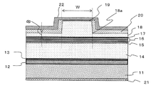
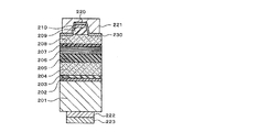
- FIG. 1 is a cross-sectional view illustrating a layer structure of a light emitting device according to the first embodiment of the present disclosure.
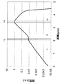
- FIG. 2 is a view showing a light distribution in the direction perpendicular to the main surface of the GaN substrate 11 of the light emitting element.
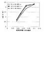
- FIG. 3 is a graph showing the dependence of ⁇ N on the light emitting element on the Al composition of the first low refractive index layer 13.
- FIG. 4A is a diagram showing the composition of the first low refractive index layer 13 and the layer thickness dependence of ⁇ N when the In composition of the first strain correction layer 12 is 4% in the light emitting element.
- FIG. 1 is a cross-sectional view illustrating a layer structure of a light emitting device according to the first embodiment of the present disclosure.
- FIG. 2 is a view showing a light distribution in the direction perpendicular to the main surface of the GaN substrate 11 of the light emitting element.
- FIG. 3 is a graph showing the dependence of ⁇ N on the light
- FIG. 4B is a diagram showing the dependency of ⁇ N on the composition and thickness of the first low refractive index layer 13 when the In composition of the first strain correction layer 12 is 3% in the light emitting element.
- FIG. 5 is a diagram comparing the calculation results of the average strain amount at each point in the stacking direction with respect to the light emitting element.
- FIG. 6 is a diagram showing a comparison of calculation results of the average strain amount at each point in the stacking direction with respect to the light emitting element.
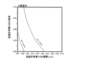
- FIG. 7 is a diagram showing a preferable atomic composition range when the first low refractive index layer 13 is InGaAlN in the light emitting element.
- FIG. 8 is a cross-sectional view illustrating a layer structure of a light emitting device according to the second embodiment of the present disclosure.
- FIG. 9 is a diagram showing a comparison of calculation results of the average strain amount at each point in the stacking direction with respect to the light emitting element.
- FIG. 10 is a diagram showing a comparison of calculation results of the average strain amount at each point in the stacking direction with respect to the light emitting element.
- FIG. 11 is a cross-sectional view showing a layer structure of a first conventional light emitting device.
- FIG. 12 is a cross-sectional view showing a layer structure of a second conventional light emitting device.
- Semiconductor laser elements used for projector light sources are required to operate not only for watt-class high-power operation but also for long-term operation of 10,000 hours or more even at high temperature operation of 50 ° C. or higher. Therefore, it is necessary to realize a semiconductor laser capable of operating at high temperature and high output in the blue region of the wavelength 445 nm band and the green region of the wavelength 530 nm band.
- the difference in refractive index between the InGaN layer widely used for the active layer and the AlGaN layer widely used for the cladding layer becomes small.
- a blue laser with a long wavelength of 445 nm and a green laser with a long wavelength of 530 nm are compared with a blue-violet laser with a wavelength of 405 nm.
- a nitride laser having an oscillation wavelength region with a long wavelength has a problem that light confinement in the vertical direction becomes small.
- the Al composition of the AlGaN layer used for the cladding layer may be increased to 0.1 or more.
- the difference in thermal expansion coefficient between the AlGaN layer and the InGaN layer used for the active layer is large.
- cracks and lattice defects occur.
- the resistance of the p-type AlGaN cladding layer increases, and the operating voltage of the device increases. For this reason, in order to suppress generation
- the In composition of the InGaN well layer in the quantum well active layer was about 0.07, but a blue laser having an oscillation wavelength of 445 nm In the InGaN well layer, the In composition needs to be about 0.15 or more. Further, in a green laser having an oscillation wavelength band of 530 nm, a high In composition InGaN layer in which the In composition of the InGaN well layer is about 0.3 or more is required.
- In the InGaN layer when the In composition increases, not only the lattice mismatch with the GaN substrate increases, but also the distance between the stable group III-V atoms of InN and GaN constituting the InGaN layer differs.
- the accumulated internal strain energy increases.
- composition separation in which the composition is separated into a region having a high In composition and a region having a low In composition is likely to occur.
- a temperature around 800 ° C. which is the temperature at which the InGaN layer is grown, when the In composition becomes a high In composition of around 0.15 or more, it becomes thermodynamically unstable and composition separation tends to occur.
- the thickness of the well layer having a high In composition is reduced to 3 nm or less, the volume of the InGaN well layer is reduced, and a barrier grows thereon. It is effective to recover the crystallinity by growing GaN or an InGaN layer having an In composition of about 0.05 or less having a small lattice mismatch with GaN to a thickness of about 10 nm or more.
- the top and bottom of the thin well layer are sandwiched between the GaN layer or InGaN having a lattice constant close to that of the GaN layer, and the InGaN well does not exceed the critical layer thickness that causes lattice defects in the InGaN layer. It becomes possible to suppress the composition separation of the layers to some extent. This is because, even in the case of a high In composition layer due to strain energy due to lattice mismatch between the well layer and the barrier layer generated at the interface between the barrier layer and the well layer, it is more thermodynamically stable if no composition separation occurs. It is. As described above, the thickness of the InGaN well layer having a high In composition needs to be as thin as about 3 nm or less.
- the Al composition of the AlGaN layer used for the cladding layer may be set as high as possible to 0.1 or more.
- the difference in lattice constant of the InGaN layer to be used is increased, and cracks and lattice defects are generated.
- the optical confinement factor in the vertical direction becomes a very small value of about 1%.
- the optical confinement factor is small, the operating carrier density in the active layer increases, and the carrier overflow from the active layer to the p-type cladding layer increases during high-temperature and high-power operation, resulting in deterioration of temperature characteristics and current-light output characteristics. This leads to a decrease in the thermal saturation level of the light output at.
- the normal direction of the substrate is referred to as a vertical direction
- the direction perpendicular to the normal direction of the substrate in the plane of the resonator end surface is referred to as a horizontal direction.
- a free-standing substrate 201 made of GaN and a substrate are formed on the substrate.
- a second buffer layer 203, and an n-side cladding layer 204, an active layer 206, and a p-side cladding layer 209 are sequentially provided on the second buffer layer.
- the function of the buffer layer is divided into the first buffer layer 202 that suppresses the occurrence of dislocations from the regrowth interface and the second buffer layer 203 that suppresses the occurrence of cracks, thereby free-standing substrate 201. It is disclosed that a high-quality AlGaN layer can be grown thereon to obtain a nitride semiconductor device having excellent electrical characteristics.
- the refractive index of the second buffer layer 202 is relatively higher than that of other layers, if the layer thickness between the second buffer layer 202 and the active layer 206 is thin, the second buffer layer 202 is confined in the waveguide. The light distribution is affected by the second buffer layer 202 having a high refractive index, and the light distribution in the vertical direction is biased toward the substrate side where the second buffer layer 202 is located.
- the effective refractive index difference ( ⁇ N) inside and outside the ridge decreases, the horizontal confinement mechanism of the light distribution becomes weak, a kink that causes nonlinearity of the current-light output characteristic occurs, and the operating current value is high.
- the n-side cladding layer 204 between the second buffer layer 202 and the active layer 206 is thickened or the n-side cladding between the substrate and the active layer so that the vertical light distribution does not spread to the second buffer layer 202.
- the stress in the n-side cladding layer 204 increases and cracks are likely to occur.
- the Al composition of the p-side cladding layer 209 is set lower than the Al composition of the n-side cladding layer 204, and the refractive index of the p-side cladding layer 209 is relatively higher than that of the n-side cladding layer 204, so that the vertical direction
- a method of making the light distribution relatively closer to the p-type layer is also conceivable, the light confinement coefficient in the active layer 206 becomes small and the temperature characteristics deteriorate.
- the present disclosure has been made to solve the above-described problems.
- An object is to realize a laser capable of suppressing the above.
- FIG. 1 is a cross-sectional view relating to the structure of the light emitting device according to the first embodiment of the present disclosure.
- the light-emitting element shown in FIG. 1 includes an n-type first strain correction layer 12 made of InGaN and having a layer thickness of 0.1 ⁇ m on a GaN substrate 11 having a principal surface of c-plane ((0001) plane).
- a first low refractive index layer 13 made of n-type AlGaN having a thickness of 0.05 ⁇ m
- a first cladding layer 14 made of n-type AlGaN
- a light guide layer 15 made of N-type GaN having a layer thickness of 0.2 ⁇ m.
- This light emitting element is a semiconductor laser device.
- a ridge 18a is formed in the second cladding layer 18, and the width (W) of the bottom of the ridge 18a is 8.0 ⁇ m.
- the p-side electrode 22 has a laminated structure of Ni, Pt, and Au, and the N-side electrode 21 has a laminated structure of Ti and Al.
- the distance between the upper portion of the ridge 18 a and the active layer 16 is 0.7 ⁇ m, and the distance between the lower end of the ridge 18 a and the active layer 16 is dp (0.05 ⁇ m).
- Si is used as the n-type dopant, and about 10 18 cm ⁇ 3 of Si is added to the n-type semiconductor layer.
- Mg is used as the p-type dopant, and Mg of about 10 19 cm ⁇ 3 is added to the p-type semiconductor layer.
- the electron barrier layer 17 is provided in order to prevent electrons confined in the active layer 16 from overflowing into the second cladding layer 18 (carrier overflow).
- the light-emitting element according to the first embodiment of the present disclosure is a ridge stripe semiconductor laser device, and the ridge 18a extends in a direction perpendicular to the paper surface of FIG. 1 and has a length of 1000 ⁇ m.
- the front end face (not shown) of the light emitting element is coated with a low reflectance (AR), and the rear end face (not shown) is coated with a high reflectance (HR). Both the front end face and the rear end face are perpendicular to the extending direction of the ridge 18a, and form a resonator between the front end face and the rear end face.
- the light emission wavelength of the light emitting element according to the first embodiment of the present disclosure is 445 nm.
- the upper limit of the Al composition of the first cladding layer 14 and the second cladding layer 18 is 0.1 or less, more preferably 0.05 or less.
- the refractive index difference between the active layer 16 and the AlGaN material is reduced, and the optical confinement factor in the vertical direction is reduced.
- the Al composition of the first cladding layer 14 and the second cladding layer 18 must be 0.03 or more.
- the Al composition of the first cladding layer 14 and the second cladding layer 18 is preferably 0.03 or more, and the upper limit of the Al composition is preferably 0.1 or less, more preferably 0.05 or less.
- the active layer 16 of the light emitting element As the active layer 16 of the light emitting element, a quantum well structure having a single well or a plurality of well layers is used. In order to obtain laser oscillation with a wavelength of 445 nm, the In composition of the well layer needs to be about 0.15. However, the lattice mismatch between InGaN and GaN with an In composition of 0.15 is about 1.6%, and when the well layer thickness is greater than 3 nm, the critical layer thickness of the well layer is greatly exceeded, resulting in lattice defects. End up. The lattice defect becomes a light absorption center, which causes an increase in the oscillation threshold current value and the operating current value of the light emitting element, leading to a decrease in reliability. Therefore, it is necessary to suppress the generation as much as possible. Therefore, the thickness of the well layer is preferably 3 nm or less.
- the well layer thickness is thin, the light confinement factor in the vertical direction of the light emitting element is lowered. Therefore, it is necessary to increase the thickness of the well layer.
- the operational carrier density of each well layer tends to vary, and the gain peak wavelength that gives the maximum gain of each well layer varies.
- the oscillation threshold current value increases.
- the number of barrier layers between the well layers increases, the increase in series resistance of the light emitting element and the influence of the slope of the potential potential of the barrier layer due to the piezo effect increase, and the operating voltage increases. .
- the oscillation threshold current value becomes large and the light emitting element has a high operating voltage. As a result, the temperature characteristics of the light emitting element are deteriorated.
- the number of well layers is 1, that is, a single quantum well structure
- the optical confinement factor is reduced and the operating carrier density is increased, so that the carrier overflow is increased and the light output that is thermally saturated in the current-light output characteristics is reduced. End up. Therefore, even if the well layer thickness is a thin well layer of 3 nm or less, the number of well layers is a double quantum well (DQW) structure with two layers, or a triple quantum well with triple layers (Triple Quantum). (Well, TQW) structure.
- DQW double quantum well
- TQW Triple Quantum
- the active layer 16 in the light emitting device of the first embodiment of the present disclosure has a double quantum well structure including two well layers made of InGaN having a thickness of 3 nm and an In composition of 0.15, and GaN as a barrier layer. .
- the Al composition of the first cladding layer 14 and the second cladding layer 18 must be 0.03 or more. In this case, when the thickness of the first cladding layer 14 is about 1.5 ⁇ m, lattice defects and cracks are likely to occur due to the difference in lattice constant between the GaN substrate 11 and the first cladding layer 14.
- the light emitting device includes the first strain correction layer 12 having compressive strain made of InGaN on the GaN substrate 11.
- the tensile strain generated in the first cladding layer 14 can be compensated, so that the average strain of the entire epitaxial layer grown on the GaN substrate 11 can be reduced, and the generation of cracks and lattice defects can be reduced. Can be suppressed.
- the vertical axis represents the logarithm of the light intensity (arbitrary unit) when the light intensity in the active layer 16 is 1, and the horizontal axis represents the semiconductor layer with the origin slightly below the surface of the GaN substrate 11.
- the position of each semiconductor layer measured along the stacking direction is represented.
- the numbers in FIG. 2 indicate the positions where each semiconductor layer exists.
- 1E-05 represents 1 ⁇ 10 ⁇ 5 .
- the light distribution in the vertical direction inside the ridge needs to be closer to the second cladding layer 18.
- the p-type impurity concentration is normally increased to 1 ⁇ 10 18 cm ⁇ 3 or more, the waveguide loss increases due to the influence of the absorption loss of free carriers due to the p-type impurity, and the current-optical output
- the light output change (slope efficiency) per unit current in the characteristics is lowered, and the temperature characteristics are lowered.
- ⁇ N needs to be in the range of 3 ⁇ 10 ⁇ 3 to 6 ⁇ 10 ⁇ 3 .
- the light emitting device includes the first low refractive index layer 13 having a refractive index smaller than that of the first cladding layer 14.
- FIG. 3 shows the calculation result of the dependency of ⁇ N with respect to.
- the layer thickness of the first cladding layer 14 is 1 ⁇ m, 1.5 ⁇ m, and 2 ⁇ m
- the In composition of the first strain correction layer 12 is 4%.
- the decrease in ⁇ N increases as the thickness of the first cladding layer 14 decreases.
- the Al composition is 0.05 or more, that is, the Al composition of the first cladding layer 14 is larger than that. It can be seen that it is necessary to use an AlGaN layer having an Al composition of at least 0.015 or more. Further, in order to set ⁇ N to 3.5 ⁇ 10 ⁇ 3 or more, AlGaN having an Al composition of 0.06 or more, that is, an Al composition that is at least 0.025 or more larger than the Al composition of the first cladding layer 14. It can be seen that it is necessary to use a layer.
- FIG. 4A and FIG. 4B show calculation results of the dependence of ⁇ N on the composition of the first low refractive index layer 13 and the layer thickness when the In composition of the first strain correction layer is 4% and 3%, respectively.
- ⁇ N does not depend much on the composition and layer thickness of the first low refractive index layer 13, but the first strain correction layer 12
- ⁇ N greatly depends on the composition and thickness of the first low refractive index layer 13. Therefore, it can be seen that the In composition of the first strain correction layer 12 should be 3% or less so as not to be affected by the first strain correction layer 12 of ⁇ N.
- the Al composition of the first low refractive index layer 13 is set to 0.06 to 0.1 and the layer thickness is set to 10 nm to 100 nm, it can be seen that ⁇ N of 4 ⁇ 10 ⁇ 3 or more can be realized.
- the In composition of the first strain correction layer 12 is 0.02
- the composition of the first low refractive index layer 13 is 0.025 higher than the Al composition of the first cladding layer 14. 06, even when the thickness of the first cladding layer 14 is 0.05 ⁇ m and the thickness of the first cladding layer 14 is 1 ⁇ m, the prevention of ⁇ N can be suppressed.
- the refractive index of the 1st low refractive index layer 13 can be made small, so that Al composition of the 1st low refractive index layer 13 is large, the optical confinement rate with respect to the active layer 16 can be enlarged, and (DELTA) N is enlarged.
- the Al composition of the first low refractive index layer 13 is preferably 0.1 or less.
- the first low refractive index layer is preferably formed of n-type Al b Ga 1-b N (0.06 ⁇ b ⁇ 0.1).
- the layer thickness of the first low refractive index layer 13 is preferably 10 nm or more and 100 nm or less.
- a well layer is In 0.15 Ga 0.85 N with a layer thickness of 3 nm
- a barrier layer is GaN with a layer thickness of 3 nm
- a double quantum well structure is adopted.
- the first strain correction layer 12, the first low refractive index layer 13, the first cladding layer 14, and the second cladding layer 18 were examined using the In composition, Al composition, and layer thickness as parameters.
- 5 and 6 show comparison results of the average strain amount of each point along the stacking direction of the light emitting device according to the first embodiment of the present disclosure. 5 and 6, the active layer 16 is expanded in the stacking direction.
- the parameters of the first strain correction layer 12, the first low refractive index layer 13, the first cladding layer 14, and the second cladding layer 18 that were examined are as shown in Tables 2 and 3.
- the parameters of the layers other than the layers shown in Table 2 and Table 3 are the same as in Table 1.
- the light emitting device has a structure in which the first strain correction layer 12 and the first low refractive index layer 13 are not provided, the thickness of the first cladding layer 14 is 1 ⁇ m, and the Al composition is 0. 0.035, the thickness of the second cladding layer 18 is 0.7 ⁇ m, and the Al composition is 0.035, the In composition of the first strain correction layer is 0.01, 0.02, 0.03.
- FIG. 5A shows the calculation result of the average strain amount at each point in the stacking direction.
- the average strain amount (Eequ (Z)) at a certain point in the stacking direction is an average value of strain in consideration of the layer thickness of each layer up to a certain point Z in the stacking direction in the structure formed on the GaN substrate 11. Yes, given by (Equation 1).
- e (z ′) is a strain at a point z ′ in the Z direction (stacking direction).
- the first cladding layer 14 has a uniform tensile strain of about 8 ⁇ 10 ⁇ 4. Therefore, the average strain amount is compensated and reduced in the region of the active layer 16 where the compressive strain of the InGaN-based material is applied, and the tensile strain is increased again in the second cladding layer 18 where the tensile strain is generated. I understand that.
- the thickness of the first strain correction layer 12 is 0.1 ⁇ m, and the composition of the first low refractive index layer 13 is 0.06, which is 0.025 higher than the Al composition of the first cladding layer.
- the first strain correction layer 12 FIG. 5 (b) shows the calculation result of the average strain amount at each point in the stacking direction when the In composition is 0.01, 0.02, and 0.03. *
- the average strain generated in the first cladding layer 14 by the first strain correction layer 12 is generated in the first cladding layer 14 with respect to the light emitting element shown in FIG. It can be seen that the average distortion is reduced.
- 5 (c) and 5 (d) show the case where the thickness of the first cladding layer 14 is 1.5 ⁇ m with respect to the light emitting device of FIG. 5 (a) and FIG. 5 (b), respectively.
- the calculation result of is shown. Even when the thickness of the first cladding layer 14 is 1.5 ⁇ m, the tensile property of the first cladding layer 14 is reduced due to the compressive strain of the first strain correction layer 12 as in the result shown in FIG. It can be seen that the distortion is compensated and reduced.
- the In composition of the first strain correction layer 12 is set to 0.1 in the range of the thickness of the first cladding layer 14 from 1.0 ⁇ m to 1.5 ⁇ m. It can be seen that the strain generated in the first cladding layer 14 can be reduced by setting between 01 and 0.03.
- the light emitting device has a structure in which the first strain correction layer 12 and the first low refractive index layer 13 are not provided, the thickness of the first cladding layer 14 is 1 ⁇ m, the Al composition is 0.06, and the second When the thickness of the cladding layer 18 is 0.7 ⁇ m and the Al composition is 0.06, each of the stacking directions in the case where the In composition of the first strain correction layer is 0.01, 0.02, and 0.03
- the calculation result of the average strain amount of the points is shown in FIG.
- the first cladding layer 14 is uniformly strained by about 1.4 ⁇ 10 ⁇ 3.
- the average strain amount is compensated and reduced in the region of the active layer 16 where the compressive strain of the InGaN-based material is applied, and the tensile strain is increased again in the second cladding layer 18 in which the tensile strain is generated.
- a relatively large strain is applied to the first cladding layer 14, and cracks and lattice defects are likely to occur in the first cladding layer 14. I understand that.
- the thickness of the first strain correction layer 12 is 0.1 ⁇ m, and the composition of the first low refractive index layer 13 is 0 than the Al composition of the first cladding layer 14. 0.025 high 0.085, the thickness of the first low refractive index layer 13 is 0.05 ⁇ m, the thickness of the first cladding layer 14 is 1 ⁇ m, and the thickness of the second cladding layer 18 is 0.7 ⁇ m.
- FIG. 6B shows the calculation result of the average strain amount at each point in the stacking direction when the In composition of the first strain correction layer 12 is 0.01, 0.02, and 0.03.
- the average strain generated in the first cladding layer 14 by the first strain correction layer 12 is the average generated in the first cladding layer 14 with respect to the structure shown in FIG. It can be seen that the distortion is reduced.
- the strain generated in the first cladding layer 14 can be reduced by setting the In composition of the first strain correction layer 12 between 0.01 and 0.03.
- FIG. 6 (c) and 6 (d) show the case where the thickness of the first cladding layer 14 is 1.5 ⁇ m with respect to the structure of FIG. 6 (a) and FIG. 6 (b), respectively.
- the calculation result of is shown. Even when the thickness of the first cladding layer 14 is 1.5 ⁇ m, the tensile property of the first cladding layer 14 is reduced due to the compressive strain of the first strain correction layer 12 as in the result shown in FIG. It can be seen that the distortion is compensated and reduced.
- the In composition of the first strain correction layer 12 is 0.01 when the thickness of the first cladding layer 14 is in the range of 1.0 ⁇ m to 1.5 ⁇ m. It can be seen that the strain generated in the first cladding layer 14 can be reduced by setting the value between 1 and 0.03.
- the thickness of the first strain correction layer 12 is set to 0.1 ⁇ m, if this layer thickness is increased, the effect of compensating the tensile strain generated in the first cladding layer 14 is large, and the tension generated in the first cladding layer 14 is increased. The effect of reducing the sexual distortion is increased.
- the first strain correction layer 12 is made too thick, lattice defects are generated in the first strain correction layer 12 due to a difference in lattice constant with the GaN substrate 11, and crystallinity is lowered. Actually, when the thickness of the first strain correction layer 12 exceeds 0.3 ⁇ m, lattice defects are likely to occur in the first strain correction layer 12.
- the thickness of the first strain correction layer is smaller than 0.1 ⁇ m, the effect of compensating the tensile stress generated in the first cladding layer 14 and the second cladding layer 18 becomes small.
- the thickness of the first strain correction layer 12 is set to 0. What is necessary is just to set between 1 micrometer or more and 0.3 micrometer or less.
- the band gap energy of the electron barrier layer 17 and the second cladding layer 18 increases, and the electron barrier layer 17 and the second cladding layer 18.
- the barrier height against electrons of the layer 18 is increased.
- carrier overflow can be reduced. For this reason, the oscillation threshold value and operating current value at the time of high-temperature operation of the light emitting element can be reduced, and the reliability of the long-term operation of the light emitting element can be improved.
- the effect of the first strain correction layer 12 causes the GaN substrate to The average strain amount of the entire layer formed on 11 is almost zero.
- compressive strain is applied to the electron barrier layer 17 and the second cladding layer 18. That is, in the light emitting element shown in FIG. 5B, carrier overflow can be reduced, and as a result, the reliability of long-term operation of the light emitting element can be improved.
- the average strain of the entire layer is reduced by setting the thickness of the first cladding layer 14 to 1 ⁇ m or less for the light emitting device shown in FIG.
- the compressive strain can be applied, and the compressive strain can be applied to the electron barrier layer 17 and the second cladding layer 18.
- the Al composition of the first cladding layer is 0.06
- the average strain of the entire layer becomes tensile strain
- the electron barrier layer 17 and the second cladding layer 18 are pulled. Sexual distortion has been added.
- the Al composition of the first cladding layer is set to 0.04 or less. preferable.
- the Al composition of the first cladding layer 14 and the second cladding layer 18 is preferably 0.03 or more.
- the Al composition is preferably 0.03 or more and 0.04 or less.
- the first low refractive index layer 13 is not limited to an AlGaN material, but may be InGaAlN having a refractive index smaller than that of an AlGaN layer having an Al composition of 0.06.
- the region indicated by is a region where the refractive index of In 1-ab Al b Ga a N is smaller than the refractive index of Al 0.05 Ga 0.95 N. That is, if the condition of (Expression 2) is satisfied, the refractive index of the first low refractive index layer 13 can be made smaller than that of AlGaN having an Al composition of 0.05. In the first low refractive index layer that satisfies this condition, ⁇ N can be increased.
- In 0.02 Al 0.12 Ga 0.86 N can be used as the first low refractive index layer 13.
- In 0.02 Al 0.12 Ga 0.86 N satisfies (Equation 1) and almost satisfies (Equation 2), which is preferable.
- the first low refractive index layer 13 for example, one or more layers of In 0.02 Al 0.12 Ga 0.86 N having a thickness of 5 nm and In 0.04 Al 0.24 Ga 0. 72 N may be alternately formed in two or more layers to form a single quantum well structure or a multiple quantum well structure.
- the thickness of each layer constituting the single quantum well structure or the multiple quantum well structure is not limited to the above.
- the light-emitting element of the present disclosure preferably has the following configuration.
- a first strain correction comprising a GaN substrate 11 as a light emitting element and a first conductivity type (n-type) In x Ga 1-x N (0 ⁇ x ⁇ 1) formed on the GaN substrate 11.
- a low refractive index layer 13 comprising a GaN substrate 11 as a light emitting element and a first conductivity type (n-type) In x Ga 1-x N (0 ⁇ x ⁇ 1) formed on the GaN substrate 11.
- the first low refractive index layer 13 is made of Al z Ga 1 -zN (0.03 ⁇ z ⁇ 0.06) of the first conductivity type and formed on the first low refractive index layer 13.
- the active layer 16 It is formed on the active layer 16 and is made of Al t Ga 1-t N (0 ⁇ t ⁇ 1) of the second conductivity type (p-type) and protrudes in the direction from the GaN substrate 11 toward the active layer.
- the second cladding layer 18 having the ridge portion 18a may be provided.
- the first low refractive index layer 13 may be a multilayer structure having an In 1-ab Ga a Al b N layer whose average atomic composition satisfies the above (formula 3) to (formula 5).
- the In 1-ab Ga a Al b N layer may be thinned to have a quantum effect.
- the first low refractive index layer may be a single quantum well structure or a double quantum well structure.
- the light emitting device according to the second embodiment of the present disclosure includes a light emitting device according to the first embodiment illustrated in FIG. 1 between the GaN substrate 11 and the first strain correction layer 12.
- the second distortion correction layer 32 and the intermediate layer 33 are provided.
- the second strain correction layer 32 is made of an AlGaN material, and the Al composition is an AlGaN layer having an Al composition of 0.01 or less.
- the intermediate layer 33 is made of a GaN layer. This intermediate layer 33 can reduce the stress generated at the interface of the first strain correction layer 12 on the substrate 11 side, compared with the case where the first strain correction layer 12 is directly laminated on the second strain correction layer 32. it can. As a result, it is possible to suppress the occurrence of lattice defects generated in the first strain correction layer 12 as compared with the case where the first strain correction layer 12 is directly formed on the second strain correction layer 32.
- each semiconductor layer, the current blocking layer 20, the n-side electrode 21, and the p-side electrode 22 from the first strain correction layer 12 to the contact layer 19 of the light emitting device according to the second embodiment is the first configuration. This is the same as the light emitting device according to the embodiment.
- the ridge stripe structure is the same as that of the light emitting device according to the first embodiment.
- the light emitting device according to the second embodiment of the present disclosure is further different from the light emitting device disclosed in the first embodiment between the GaN substrate 11 and the first strain correction layer 12.
- 11 includes a second strain correction layer 32 made of Al s Ga 1-s N (0 ⁇ s ⁇ 0.01) of the first conductivity type (n-type) from the 11 side, and further includes the second strain correction layer 32 and the first strain.
- the intermediate layer 33 made of GaN of the first conductivity type (n-type) is provided between the correction layer 12 and the correction layer 12.
- the structural parameters of the light emitting device according to the second embodiment of the present disclosure are as shown in Table 4.
- FIG. 9 and FIG. 10 compare and show the calculation results of the average strain amount at each point along the stacking direction of the light emitting device according to the second embodiment of the present disclosure.
- the active layer 16 is expanded in the stacking direction.
- the parameters of the first strain correction layer 12, the first low refractive index layer 13, the first cladding layer 14, and the second cladding layer 18 that were examined are as shown in Tables 5 and 6.
- the parameters of the layers other than the layers shown in Table 5 and Table 6 are the same as in Table 4.
- the light emission wavelength of the light emitting element according to the second embodiment of the present disclosure is 445 nm.
- the IN composition, Al composition, and layer thickness of the second strain correction layer 32, the first low refractive index layer 13, the first cladding layer 14, and the second cladding layer 18 were examined as parameters.
- FIG. 9A shows a second strain correction layer 32, an intermediate layer 33, a first strain correction layer 12, and a first low refractive index layer in the light emitting device according to the second embodiment of the present disclosure shown in FIG.
- the Al composition is 0.035
- the AlGaN second cladding layer 18 is 0.7 ⁇ m thick
- the Al composition is 0.035. The calculation result of the average distortion amount of each point of the lamination direction in is shown.
- the first cladding layer 14 is uniformly 8 A tensile strain of about ⁇ 10 ⁇ 4 is applied, and the average strain amount is compensated and reduced in the region of the active layer 16 where the compressive strain of the InGaN-based material is applied, and the second cladding layer 18 in which the tensile strain is generated. It can be seen that the tensile strain increases again.
- the layer thickness of the second strain correction layer 32 is 1.0 ⁇ m, the Al composition is 0.01 and 0.005, and the layer thickness of the intermediate layer 33 is.
- the thickness of the first strain correction layer 12 is 0.1 ⁇ m, the composition of the first low refractive index layer 13 is 0.06, which is 0.025 higher than the Al composition of the first cladding layer 14, and the first low
- the layer thickness of the refractive index layer 13 is 0.05 ⁇ m
- the layer thickness of the first cladding layer 14 is 1 ⁇ m
- the layer thickness of the AlGaN second cladding layer 18 is 0.7 ⁇ m
- the In of the first strain correction layer 12 The calculation result of the average distortion amount of each point of the lamination direction when a composition is 0.02 is shown.
- the average strain generated in the first cladding layer 14 is the same as that shown in FIG. 5B, regardless of whether the Al composition of the second strain correction layer 32 is 0.005 or 0.01. It can be seen that the light emitting element shown in FIG.
- the strain of the entire layer is 4 ⁇ 10 ⁇ 4 at the maximum, which is about 1/5 of the light emitting device shown in FIG. The amount of distortion.
- the strain is almost zero. From this, it can be seen that the generation of lattice defects in the first strain correction layer 12 and the first low refractive index layer 13 can be suppressed in the light emitting element shown in FIG.
- the tensile strain amount of the first cladding layer 14 is larger than the tensile strain amount of the first cladding layer 14 in the light emitting element shown in FIG. small.
- the compressive strain of the first strain correction layer 12 and the average strain of the tensile strain of the first cladding layer 14 are reduced. Because.
- FIG. 9 (c) and 9 (d) show the case where the thickness of the first cladding layer 14 is 1.5 ⁇ m, compared to the structure of FIG. 9 (a) and FIG. 9 (b), respectively.
- the calculation result of is shown.
- the first strain correction is performed by using the second strain correction layer 32 having a weak tensile strain, similarly to the result shown in FIG. 9B. It can be seen that the compressive strain of the layer 12 and the average strain of the tensile strain of the first cladding layer 14 are reduced.
- the thickness of the first strain correction layer 12 is set to 0.1 ⁇ m. If this layer thickness is increased, the first cladding layer 14 is generated. The tensile strain compensation effect is increased, and the tensile strain reduction effect generated in the first cladding layer 14 is increased.
- the layer thickness of the first strain correction layer 12 is set to 0. What is necessary is just to set to the range from 1 micrometer to 0.3 micrometer.
- the average strain of the entire layer is reduced by setting the thickness of the first cladding layer 14 to 1 ⁇ m or less in the light emitting device shown in FIG. 9B.
- the compressive strain can be applied, and the compressive strain can be applied to the electron barrier layer 17 and the second cladding layer 18.
- the Al composition of the first cladding layer is 0.06
- the average strain of the entire layer becomes tensile strain
- the electron barrier layer 17 and the second cladding layer 18 are pulled. Distortion has occurred.
- the Al composition of the first cladding layer is set to 0.04 or less. preferable.
- FIG. 10A shows a second strain correction layer 32, an intermediate layer 33, a first strain correction layer 12, and a first low refractive index layer in the light emitting device according to the second embodiment of the present disclosure shown in FIG. 13 is a structure in which the thickness of the first cladding layer 14 is 1 ⁇ m, the Al composition is 0.06, the thickness of the second cladding layer 18 is 0.7 ⁇ m, and the Al composition is 0.06. The calculation result of the average distortion amount of each point of a direction is shown.
- the N-type first cladding layer 14 is uniform.
- the tensile strain of about 1.4 ⁇ 10 ⁇ 3 is applied to the active layer 16, and the average strain amount is compensated and reduced in the region of the active layer 16 where the compressive strain of the INGaN-based material is applied, and the tensile strain is generated. It can be seen that the tensile strain is increased again in the two clad layer 18.
- the thickness of the second strain correction layer 32 is 1.0 ⁇ m, the Al composition is 0.01 and 0.005, and the intermediate layer 33 is used.
- the thickness of the first strain correction layer 12 is 0.1 ⁇ m, and the composition of the first low refractive index layer 13 is 0.025 higher than the Al composition of the first cladding layer 14 by 0.085.
- the calculation results of the average strain amount at each point in the stacking direction when the In composition of the layer is 0.01, 0.02, and 0.03 are shown.
- the Al composition of the first cladding layer and the second cladding layer is 0.035 to 0.005.
- the Al composition of the second strain correction layer 32 is 0.005 to 0.01 in the range of 06 and the thickness of the first cladding layer 14 in the range of 1.0 ⁇ m to 1.5 ⁇ m, the first cladding It can be seen that strain generated in the layer 14 can be reduced.
- the In composition and the layer thickness of the well layer in the active layer 16 are not limited to the above, and the composition and the layer thickness of the barrier layer are not limited to the above.
- the In composition and layer thickness of the well layer in the active layer 16 and the composition and layer thickness of the barrier layer can be appropriately selected according to the emission wavelength of the light emitting element.
- the emission wavelength can be made larger than 445 nm, and light emission such as blue or green can be obtained.
- the emission wavelength can be set to 530 nm.
- the Al compositions of the first cladding layer 14 and the second cladding layer are equal, but this is not always necessary.
- the Al composition may be different.
- the layer structure of the light-emitting element is formed on the c-plane of the GaN substrate 11.
- the layer structure is not limited to the c-plane, but is a plane inclined from the c-plane, that is, GaN.
- the layer structure of the light emitting element may be formed on the off substrate, or the layer structure of the light emitting element may be formed on the GaN substrate having the m-plane, r-plane or a-plane as the main surface.
- the semiconductor laser device has been discussed.
- the technology according to the present disclosure can also be applied to the LED device, and the generation of cracks and lattice defects is suppressed.
- An LED element having a longer wavelength band than blue can be realized.
- the invention according to the present disclosure realizes a watt-class light source that has excellent temperature characteristics capable of operating at an ultrahigh output of 1 watt or more and can guarantee long-term reliability in a light emitting device having a wavelength of 445 nm or more.
- it can be used for watt-class light sources used for projector light sources.
- the light source is not limited to the projector light source, but can be used as a light source for an in-vehicle headlamp, for example, or can be used as an illumination light source for a stadium.
- GaN substrate 12
- First strain correction layer 13
- First low refractive index layer 14
- First cladding layer 15
- Light guide layer 16
- Active layer 17
- Electron barrier layer 18
- Second cladding layer 19
- Contact layer 20
- Current blocking layer 21
- N-side electrode 22
- p Side electrode 32
- Second strain correction layer 33
Landscapes
- Physics & Mathematics (AREA)
- Condensed Matter Physics & Semiconductors (AREA)
- General Physics & Mathematics (AREA)
- Electromagnetism (AREA)
- Optics & Photonics (AREA)
- Geometry (AREA)
- Semiconductor Lasers (AREA)
- Led Devices (AREA)
Abstract
L'invention concerne un élément électroluminescent muni : d'un substrat de GaN (11) ; d'une première couche de correction de distorsion (12), qui est formée sur le substrat de GaN (11), et est formée de type n
InxGa1-xN (0<x≤1) ; et d'une première couche à indice de réfraction faible (13), qui est formée sur la première couche de correction de distorsion (12), et est formée de type n In1-a-bGaaAlbN, ladite première couche à indice de réfraction faible ayant des relations de (a/0.98)+(b/0.8)≥1, (a/1.02)+(b/0.85)≤1, and (a/1.03)+(b/0.68)≥1. L'élément électroluminescent est en outre muni : d'une première couche de gainage (14), qui est formée sur la première couche à indice de réfraction faible (13), et est formée de type n AlzGa1-zN(0.03≤z≤0.06), ladite première couche de gainage ayant un indice de réfraction plus élevé que la première couche à indice de réfraction faible (13) ; et d'une couche active (16) formée sur la première couche de gainage (14).
Priority Applications (3)
| Application Number | Priority Date | Filing Date | Title |
|---|---|---|---|
| CN201680032473.7A CN107615602B (zh) | 2015-06-08 | 2016-05-25 | 发光元件 |
| JP2017523099A JP6706805B2 (ja) | 2015-06-08 | 2016-05-25 | 半導体レーザ装置 |
| US15/832,248 US10164408B2 (en) | 2015-06-08 | 2017-12-05 | Light emitting element |
Applications Claiming Priority (2)
| Application Number | Priority Date | Filing Date | Title |
|---|---|---|---|
| JP2015-116141 | 2015-06-08 | ||
| JP2015116141 | 2015-06-08 |
Related Child Applications (1)
| Application Number | Title | Priority Date | Filing Date |
|---|---|---|---|
| US15/832,248 Continuation US10164408B2 (en) | 2015-06-08 | 2017-12-05 | Light emitting element |
Publications (1)
| Publication Number | Publication Date |
|---|---|
| WO2016199363A1 true WO2016199363A1 (fr) | 2016-12-15 |
Family
ID=57503771
Family Applications (1)
| Application Number | Title | Priority Date | Filing Date |
|---|---|---|---|
| PCT/JP2016/002523 Ceased WO2016199363A1 (fr) | 2015-06-08 | 2016-05-25 | Élément électroluminescent |
Country Status (4)
| Country | Link |
|---|---|
| US (1) | US10164408B2 (fr) |
| JP (1) | JP6706805B2 (fr) |
| CN (1) | CN107615602B (fr) |
| WO (1) | WO2016199363A1 (fr) |
Cited By (3)
| Publication number | Priority date | Publication date | Assignee | Title |
|---|---|---|---|---|
| WO2019187583A1 (fr) * | 2018-03-30 | 2019-10-03 | パナソニックIpマネジメント株式会社 | Élément électroluminescent à semi-conducteur |
| JP2022511728A (ja) * | 2018-11-19 | 2022-02-01 | オスラム オプト セミコンダクターズ ゲゼルシャフト ミット ベシュレンクテル ハフツング | 端面発光半導体レーザ |
| US11322908B2 (en) * | 2017-05-01 | 2022-05-03 | Nuvoton Technology Corporation Japan | Nitride light emitter |
Families Citing this family (3)
| Publication number | Priority date | Publication date | Assignee | Title |
|---|---|---|---|---|
| CN109075530B (zh) * | 2016-05-13 | 2021-01-12 | 松下半导体解决方案株式会社 | 氮化物类发光元件 |
| WO2020158254A1 (fr) * | 2019-01-30 | 2020-08-06 | パナソニックセミコンダクターソリューションズ株式会社 | Élément électroluminescent à semi-conducteur |
| CN115088149B (zh) * | 2020-02-13 | 2024-12-17 | 三菱电机株式会社 | 半导体激光装置 |
Citations (5)
| Publication number | Priority date | Publication date | Assignee | Title |
|---|---|---|---|---|
| JP2003060314A (ja) * | 2002-08-09 | 2003-02-28 | Matsushita Electric Ind Co Ltd | 窒化物半導体素子 |
| JP2003249463A (ja) * | 2002-12-24 | 2003-09-05 | Nichia Chem Ind Ltd | 窒化物半導体基板の製造方法 |
| JP2003282862A (ja) * | 2002-03-22 | 2003-10-03 | Sharp Corp | 窒化物半導体層、窒化物半導体素子とその製造方法 |
| JP2006080374A (ja) * | 2004-09-10 | 2006-03-23 | Sharp Corp | 窒化物半導体の製造装置および窒化物半導体レーザ素子 |
| US20080181274A1 (en) * | 2006-12-28 | 2008-07-31 | Nichia Corporation | Nitride semiconductor laser element |
Family Cites Families (8)
| Publication number | Priority date | Publication date | Assignee | Title |
|---|---|---|---|---|
| US6144683A (en) * | 1998-01-07 | 2000-11-07 | Xerox Corporation | Red, infrared, and blue stacked laser diode array by wafer fusion |
| JP4291960B2 (ja) | 2001-03-09 | 2009-07-08 | 日亜化学工業株式会社 | 窒化物半導体素子 |
| JP4788138B2 (ja) | 2004-12-10 | 2011-10-05 | 日亜化学工業株式会社 | 窒化物半導体素子 |
| JP4978454B2 (ja) * | 2006-12-28 | 2012-07-18 | 日亜化学工業株式会社 | 窒化物半導体レーザ素子 |
| EP2497168A1 (fr) * | 2009-11-05 | 2012-09-12 | The Regents of the University of California | Diodes laser de nitrure-iii {20-21} semi-polaires dotées de miroirs gravés |
| KR20130141546A (ko) * | 2010-10-26 | 2013-12-26 | 더 리전츠 오브 더 유니버시티 오브 캘리포니아 | 기판 및 에피택셜층 패터닝에 의한 iii-족 질화물 헤테로구조들 내의 스트레인 완화의 제한 |
| US20130100978A1 (en) * | 2011-10-24 | 2013-04-25 | The Regents Of The University Of California | Hole blocking layer for the prevention of hole overflow and non-radiative recombination at defects outside the active region |
| CN104319631B (zh) * | 2014-09-28 | 2017-04-26 | 北京大学东莞光电研究院 | 一种制备GaN基激光器的方法以及一种GaN基激光器 |
-
2016
- 2016-05-25 WO PCT/JP2016/002523 patent/WO2016199363A1/fr not_active Ceased
- 2016-05-25 JP JP2017523099A patent/JP6706805B2/ja active Active
- 2016-05-25 CN CN201680032473.7A patent/CN107615602B/zh active Active
-
2017
- 2017-12-05 US US15/832,248 patent/US10164408B2/en active Active
Patent Citations (5)
| Publication number | Priority date | Publication date | Assignee | Title |
|---|---|---|---|---|
| JP2003282862A (ja) * | 2002-03-22 | 2003-10-03 | Sharp Corp | 窒化物半導体層、窒化物半導体素子とその製造方法 |
| JP2003060314A (ja) * | 2002-08-09 | 2003-02-28 | Matsushita Electric Ind Co Ltd | 窒化物半導体素子 |
| JP2003249463A (ja) * | 2002-12-24 | 2003-09-05 | Nichia Chem Ind Ltd | 窒化物半導体基板の製造方法 |
| JP2006080374A (ja) * | 2004-09-10 | 2006-03-23 | Sharp Corp | 窒化物半導体の製造装置および窒化物半導体レーザ素子 |
| US20080181274A1 (en) * | 2006-12-28 | 2008-07-31 | Nichia Corporation | Nitride semiconductor laser element |
Cited By (10)
| Publication number | Priority date | Publication date | Assignee | Title |
|---|---|---|---|---|
| US11322908B2 (en) * | 2017-05-01 | 2022-05-03 | Nuvoton Technology Corporation Japan | Nitride light emitter |
| JP2022180584A (ja) * | 2017-05-01 | 2022-12-06 | ヌヴォトンテクノロジージャパン株式会社 | 窒化物系発光装置 |
| JP7478205B2 (ja) | 2017-05-01 | 2024-05-02 | ヌヴォトンテクノロジージャパン株式会社 | 窒化物系発光装置 |
| WO2019187583A1 (fr) * | 2018-03-30 | 2019-10-03 | パナソニックIpマネジメント株式会社 | Élément électroluminescent à semi-conducteur |
| JPWO2019187583A1 (ja) * | 2018-03-30 | 2020-07-16 | パナソニック株式会社 | 半導体発光素子 |
| CN111937261A (zh) * | 2018-03-30 | 2020-11-13 | 松下半导体解决方案株式会社 | 半导体发光元件 |
| US11070028B2 (en) | 2018-03-30 | 2021-07-20 | Nuvoton Technology Corporation Japan | Semiconductor light emitting element |
| JP2022511728A (ja) * | 2018-11-19 | 2022-02-01 | オスラム オプト セミコンダクターズ ゲゼルシャフト ミット ベシュレンクテル ハフツング | 端面発光半導体レーザ |
| JP7239696B2 (ja) | 2018-11-19 | 2023-03-14 | エイエムエス-オスラム インターナショナル ゲーエムベーハー | 端面発光半導体レーザ |
| US12021350B2 (en) | 2018-11-19 | 2024-06-25 | Osram Opto Semiconductors Gmbh | Edge-emitting semiconductor laser |
Also Published As
| Publication number | Publication date |
|---|---|
| CN107615602B (zh) | 2020-05-01 |
| US10164408B2 (en) | 2018-12-25 |
| JP6706805B2 (ja) | 2020-06-10 |
| JPWO2016199363A1 (ja) | 2018-03-22 |
| US20180109076A1 (en) | 2018-04-19 |
| CN107615602A (zh) | 2018-01-19 |
Similar Documents
| Publication | Publication Date | Title |
|---|---|---|
| JP6255939B2 (ja) | 窒化物半導体レーザ素子 | |
| KR100837404B1 (ko) | 반도체 광전 소자 | |
| JP6706805B2 (ja) | 半導体レーザ装置 | |
| JP4328366B2 (ja) | 半導体素子 | |
| JP3433038B2 (ja) | 半導体発光装置 | |
| US9184565B2 (en) | Semiconductor light-emitting element | |
| CN102474077B (zh) | 氮化物半导体激光二极管 | |
| JP6941771B2 (ja) | 半導体発光素子 | |
| JP2001237457A (ja) | 発光素子 | |
| JPH11298090A (ja) | 窒化物半導体素子 | |
| JPWO2019187583A1 (ja) | 半導体発光素子 | |
| CN103956653A (zh) | 减小GaN基蓝紫光端发射激光器电子泄漏的方法 | |
| JP2005302784A (ja) | 半導体発光素子及びその製造方法 | |
| US9214789B2 (en) | Semiconductor light emitting element | |
| JPWO2017017928A1 (ja) | 窒化物半導体レーザ素子 | |
| JP2019041102A (ja) | レーザダイオード | |
| JP5344676B2 (ja) | 発光素子用基板および発光素子 | |
| KR101161970B1 (ko) | Ⅲ족 질화물 반도체 레이저 다이오드 | |
| JP4254373B2 (ja) | 窒化物半導体素子 | |
| JP2009302429A (ja) | 窒化物半導体レーザ | |
| JP2008177624A5 (fr) | ||
| JP2006324690A (ja) | 半導体レーザ、半導体発光素子、及び、その製造方法 | |
| US7522645B2 (en) | Nitride-based semiconductor laser device |
Legal Events
| Date | Code | Title | Description |
|---|---|---|---|
| 121 | Ep: the epo has been informed by wipo that ep was designated in this application |
Ref document number: 16807080 Country of ref document: EP Kind code of ref document: A1 |
|
| ENP | Entry into the national phase |
Ref document number: 2017523099 Country of ref document: JP Kind code of ref document: A |
|
| NENP | Non-entry into the national phase |
Ref country code: DE |
|
| 122 | Ep: pct application non-entry in european phase |
Ref document number: 16807080 Country of ref document: EP Kind code of ref document: A1 |