WO2017006815A1 - Registre à décalage, dispositif d'affichage le comportant et procédé de commande d'un registre à décalage - Google Patents
Registre à décalage, dispositif d'affichage le comportant et procédé de commande d'un registre à décalage Download PDFInfo
- Publication number
- WO2017006815A1 WO2017006815A1 PCT/JP2016/069202 JP2016069202W WO2017006815A1 WO 2017006815 A1 WO2017006815 A1 WO 2017006815A1 JP 2016069202 W JP2016069202 W JP 2016069202W WO 2017006815 A1 WO2017006815 A1 WO 2017006815A1
- Authority
- WO
- WIPO (PCT)
- Prior art keywords
- output
- conduction terminal
- level
- terminal
- output control
- Prior art date
- Legal status (The legal status is an assumption and is not a legal conclusion. Google has not performed a legal analysis and makes no representation as to the accuracy of the status listed.)
- Ceased
Links
Images








Classifications
-
- G—PHYSICS
- G06—COMPUTING OR CALCULATING; COUNTING
- G06F—ELECTRIC DIGITAL DATA PROCESSING
- G06F3/00—Input arrangements for transferring data to be processed into a form capable of being handled by the computer; Output arrangements for transferring data from processing unit to output unit, e.g. interface arrangements
- G06F3/01—Input arrangements or combined input and output arrangements for interaction between user and computer
- G06F3/03—Arrangements for converting the position or the displacement of a member into a coded form
- G06F3/041—Digitisers, e.g. for touch screens or touch pads, characterised by the transducing means
- G06F3/0412—Digitisers structurally integrated in a display
-
- G—PHYSICS
- G02—OPTICS
- G02F—OPTICAL DEVICES OR ARRANGEMENTS FOR THE CONTROL OF LIGHT BY MODIFICATION OF THE OPTICAL PROPERTIES OF THE MEDIA OF THE ELEMENTS INVOLVED THEREIN; NON-LINEAR OPTICS; FREQUENCY-CHANGING OF LIGHT; OPTICAL LOGIC ELEMENTS; OPTICAL ANALOGUE/DIGITAL CONVERTERS
- G02F1/00—Devices or arrangements for the control of the intensity, colour, phase, polarisation or direction of light arriving from an independent light source, e.g. switching, gating or modulating; Non-linear optics
- G02F1/01—Devices or arrangements for the control of the intensity, colour, phase, polarisation or direction of light arriving from an independent light source, e.g. switching, gating or modulating; Non-linear optics for the control of the intensity, phase, polarisation or colour
- G02F1/13—Devices or arrangements for the control of the intensity, colour, phase, polarisation or direction of light arriving from an independent light source, e.g. switching, gating or modulating; Non-linear optics for the control of the intensity, phase, polarisation or colour based on liquid crystals, e.g. single liquid crystal display cells
- G02F1/133—Constructional arrangements; Operation of liquid crystal cells; Circuit arrangements
- G02F1/1333—Constructional arrangements; Manufacturing methods
- G02F1/13338—Input devices, e.g. touch panels
-
- G—PHYSICS
- G02—OPTICS
- G02F—OPTICAL DEVICES OR ARRANGEMENTS FOR THE CONTROL OF LIGHT BY MODIFICATION OF THE OPTICAL PROPERTIES OF THE MEDIA OF THE ELEMENTS INVOLVED THEREIN; NON-LINEAR OPTICS; FREQUENCY-CHANGING OF LIGHT; OPTICAL LOGIC ELEMENTS; OPTICAL ANALOGUE/DIGITAL CONVERTERS
- G02F1/00—Devices or arrangements for the control of the intensity, colour, phase, polarisation or direction of light arriving from an independent light source, e.g. switching, gating or modulating; Non-linear optics
- G02F1/01—Devices or arrangements for the control of the intensity, colour, phase, polarisation or direction of light arriving from an independent light source, e.g. switching, gating or modulating; Non-linear optics for the control of the intensity, phase, polarisation or colour
- G02F1/13—Devices or arrangements for the control of the intensity, colour, phase, polarisation or direction of light arriving from an independent light source, e.g. switching, gating or modulating; Non-linear optics for the control of the intensity, phase, polarisation or colour based on liquid crystals, e.g. single liquid crystal display cells
- G02F1/133—Constructional arrangements; Operation of liquid crystal cells; Circuit arrangements
- G02F1/1333—Constructional arrangements; Manufacturing methods
- G02F1/1343—Electrodes
- G02F1/134309—Electrodes characterised by their geometrical arrangement
-
- G—PHYSICS
- G02—OPTICS
- G02F—OPTICAL DEVICES OR ARRANGEMENTS FOR THE CONTROL OF LIGHT BY MODIFICATION OF THE OPTICAL PROPERTIES OF THE MEDIA OF THE ELEMENTS INVOLVED THEREIN; NON-LINEAR OPTICS; FREQUENCY-CHANGING OF LIGHT; OPTICAL LOGIC ELEMENTS; OPTICAL ANALOGUE/DIGITAL CONVERTERS
- G02F1/00—Devices or arrangements for the control of the intensity, colour, phase, polarisation or direction of light arriving from an independent light source, e.g. switching, gating or modulating; Non-linear optics
- G02F1/01—Devices or arrangements for the control of the intensity, colour, phase, polarisation or direction of light arriving from an independent light source, e.g. switching, gating or modulating; Non-linear optics for the control of the intensity, phase, polarisation or colour
- G02F1/13—Devices or arrangements for the control of the intensity, colour, phase, polarisation or direction of light arriving from an independent light source, e.g. switching, gating or modulating; Non-linear optics for the control of the intensity, phase, polarisation or colour based on liquid crystals, e.g. single liquid crystal display cells
- G02F1/133—Constructional arrangements; Operation of liquid crystal cells; Circuit arrangements
- G02F1/136—Liquid crystal cells structurally associated with a semi-conducting layer or substrate, e.g. cells forming part of an integrated circuit
- G02F1/1362—Active matrix addressed cells
- G02F1/136286—Wiring, e.g. gate line, drain line
-
- G—PHYSICS
- G06—COMPUTING OR CALCULATING; COUNTING
- G06F—ELECTRIC DIGITAL DATA PROCESSING
- G06F3/00—Input arrangements for transferring data to be processed into a form capable of being handled by the computer; Output arrangements for transferring data from processing unit to output unit, e.g. interface arrangements
- G06F3/01—Input arrangements or combined input and output arrangements for interaction between user and computer
- G06F3/03—Arrangements for converting the position or the displacement of a member into a coded form
- G06F3/041—Digitisers, e.g. for touch screens or touch pads, characterised by the transducing means
- G06F3/0416—Control or interface arrangements specially adapted for digitisers
- G06F3/0418—Control or interface arrangements specially adapted for digitisers for error correction or compensation, e.g. based on parallax, calibration or alignment
- G06F3/04184—Synchronisation with the driving of the display or the backlighting unit to avoid interferences generated internally
-
- G—PHYSICS
- G09—EDUCATION; CRYPTOGRAPHY; DISPLAY; ADVERTISING; SEALS
- G09G—ARRANGEMENTS OR CIRCUITS FOR CONTROL OF INDICATING DEVICES USING STATIC MEANS TO PRESENT VARIABLE INFORMATION
- G09G3/00—Control arrangements or circuits, of interest only in connection with visual indicators other than cathode-ray tubes
- G09G3/20—Control arrangements or circuits, of interest only in connection with visual indicators other than cathode-ray tubes for presentation of an assembly of a number of characters, e.g. a page, by composing the assembly by combination of individual elements arranged in a matrix no fixed position being assigned to or needed to be assigned to the individual characters or partial characters
- G09G3/34—Control arrangements or circuits, of interest only in connection with visual indicators other than cathode-ray tubes for presentation of an assembly of a number of characters, e.g. a page, by composing the assembly by combination of individual elements arranged in a matrix no fixed position being assigned to or needed to be assigned to the individual characters or partial characters by control of light from an independent source
- G09G3/36—Control arrangements or circuits, of interest only in connection with visual indicators other than cathode-ray tubes for presentation of an assembly of a number of characters, e.g. a page, by composing the assembly by combination of individual elements arranged in a matrix no fixed position being assigned to or needed to be assigned to the individual characters or partial characters by control of light from an independent source using liquid crystals
- G09G3/3611—Control of matrices with row and column drivers
- G09G3/3674—Details of drivers for scan electrodes
- G09G3/3677—Details of drivers for scan electrodes suitable for active matrices only
-
- G—PHYSICS
- G11—INFORMATION STORAGE
- G11C—STATIC STORES
- G11C19/00—Digital stores in which the information is moved stepwise, e.g. shift registers
- G11C19/28—Digital stores in which the information is moved stepwise, e.g. shift registers using semiconductor elements
-
- G—PHYSICS
- G11—INFORMATION STORAGE
- G11C—STATIC STORES
- G11C7/00—Arrangements for writing information into, or reading information out from, a digital store
- G11C7/02—Arrangements for writing information into, or reading information out from, a digital store with means for avoiding parasitic signals
-
- H—ELECTRICITY
- H10—SEMICONDUCTOR DEVICES; ELECTRIC SOLID-STATE DEVICES NOT OTHERWISE PROVIDED FOR
- H10D—INORGANIC ELECTRIC SEMICONDUCTOR DEVICES
- H10D86/00—Integrated devices formed in or on insulating or conducting substrates, e.g. formed in silicon-on-insulator [SOI] substrates or on stainless steel or glass substrates
- H10D86/40—Integrated devices formed in or on insulating or conducting substrates, e.g. formed in silicon-on-insulator [SOI] substrates or on stainless steel or glass substrates characterised by multiple TFTs
- H10D86/421—Integrated devices formed in or on insulating or conducting substrates, e.g. formed in silicon-on-insulator [SOI] substrates or on stainless steel or glass substrates characterised by multiple TFTs having a particular composition, shape or crystalline structure of the active layer
- H10D86/423—Integrated devices formed in or on insulating or conducting substrates, e.g. formed in silicon-on-insulator [SOI] substrates or on stainless steel or glass substrates characterised by multiple TFTs having a particular composition, shape or crystalline structure of the active layer comprising semiconductor materials not belonging to the Group IV, e.g. InGaZnO
-
- H—ELECTRICITY
- H10—SEMICONDUCTOR DEVICES; ELECTRIC SOLID-STATE DEVICES NOT OTHERWISE PROVIDED FOR
- H10D—INORGANIC ELECTRIC SEMICONDUCTOR DEVICES
- H10D86/00—Integrated devices formed in or on insulating or conducting substrates, e.g. formed in silicon-on-insulator [SOI] substrates or on stainless steel or glass substrates
- H10D86/40—Integrated devices formed in or on insulating or conducting substrates, e.g. formed in silicon-on-insulator [SOI] substrates or on stainless steel or glass substrates characterised by multiple TFTs
- H10D86/441—Interconnections, e.g. scanning lines
-
- H—ELECTRICITY
- H10—SEMICONDUCTOR DEVICES; ELECTRIC SOLID-STATE DEVICES NOT OTHERWISE PROVIDED FOR
- H10D—INORGANIC ELECTRIC SEMICONDUCTOR DEVICES
- H10D86/00—Integrated devices formed in or on insulating or conducting substrates, e.g. formed in silicon-on-insulator [SOI] substrates or on stainless steel or glass substrates
- H10D86/40—Integrated devices formed in or on insulating or conducting substrates, e.g. formed in silicon-on-insulator [SOI] substrates or on stainless steel or glass substrates characterised by multiple TFTs
- H10D86/60—Integrated devices formed in or on insulating or conducting substrates, e.g. formed in silicon-on-insulator [SOI] substrates or on stainless steel or glass substrates characterised by multiple TFTs wherein the TFTs are in active matrices
-
- G—PHYSICS
- G02—OPTICS
- G02F—OPTICAL DEVICES OR ARRANGEMENTS FOR THE CONTROL OF LIGHT BY MODIFICATION OF THE OPTICAL PROPERTIES OF THE MEDIA OF THE ELEMENTS INVOLVED THEREIN; NON-LINEAR OPTICS; FREQUENCY-CHANGING OF LIGHT; OPTICAL LOGIC ELEMENTS; OPTICAL ANALOGUE/DIGITAL CONVERTERS
- G02F2201/00—Constructional arrangements not provided for in groups G02F1/00 - G02F7/00
- G02F2201/12—Constructional arrangements not provided for in groups G02F1/00 - G02F7/00 electrode
- G02F2201/121—Constructional arrangements not provided for in groups G02F1/00 - G02F7/00 electrode common or background
-
- G—PHYSICS
- G02—OPTICS
- G02F—OPTICAL DEVICES OR ARRANGEMENTS FOR THE CONTROL OF LIGHT BY MODIFICATION OF THE OPTICAL PROPERTIES OF THE MEDIA OF THE ELEMENTS INVOLVED THEREIN; NON-LINEAR OPTICS; FREQUENCY-CHANGING OF LIGHT; OPTICAL LOGIC ELEMENTS; OPTICAL ANALOGUE/DIGITAL CONVERTERS
- G02F2201/00—Constructional arrangements not provided for in groups G02F1/00 - G02F7/00
- G02F2201/12—Constructional arrangements not provided for in groups G02F1/00 - G02F7/00 electrode
- G02F2201/123—Constructional arrangements not provided for in groups G02F1/00 - G02F7/00 electrode pixel
-
- G—PHYSICS
- G09—EDUCATION; CRYPTOGRAPHY; DISPLAY; ADVERTISING; SEALS
- G09G—ARRANGEMENTS OR CIRCUITS FOR CONTROL OF INDICATING DEVICES USING STATIC MEANS TO PRESENT VARIABLE INFORMATION
- G09G2310/00—Command of the display device
- G09G2310/02—Addressing, scanning or driving the display screen or processing steps related thereto
- G09G2310/0264—Details of driving circuits
- G09G2310/0286—Details of a shift registers arranged for use in a driving circuit
Definitions
- the present invention relates to a shift register, and more particularly to a shift register provided in a display device or the like provided with a touch panel.
- an active matrix type liquid crystal display device having a display unit including a plurality of source bus lines (video signal lines) and a plurality of gate bus lines (scanning signal lines) is known.
- a gate driver scanning signal line drive circuit
- IC Integrated Circuit
- the display portion of the active matrix type liquid crystal display device corresponds to each of a plurality of source bus lines, a plurality of gate bus lines, and intersections of the plurality of source bus lines and the plurality of gate bus lines. And a plurality of pixel formation portions provided.
- the plurality of pixel forming portions are arranged in a matrix to form a pixel array.
- Each pixel formation unit holds a thin film transistor, which is a switching element in which a gate terminal is connected to a gate bus line passing through a corresponding intersection and a source terminal is connected to a source bus line passing through the intersection, and a pixel voltage value It includes a pixel capacity and the like.
- the active matrix liquid crystal display device is also provided with the gate driver described above and a source driver (video signal line driving circuit) for driving the source bus line.
- the video signal indicating the pixel voltage value is transmitted through the source bus line.
- each source bus line cannot transmit video signals indicating pixel voltage values for a plurality of rows at a time (simultaneously).
- the writing (charging) of the video signal to the pixel capacitors in the above-described pixel formation portion arranged in a matrix is sequentially performed row by row. Therefore, the gate driver is constituted by a shift register having a plurality of stages so that a plurality of gate bus lines are sequentially selected for a predetermined period. Then, by sequentially outputting active scanning signals from each stage of the shift register, writing of video signals to the pixel capacitors is sequentially performed row by row as described above.
- a circuit constituting each stage of the shift register is referred to as a “unit circuit”. Further, selecting one by one sequentially from the first gate bus line to the last gate bus line is simply referred to as “scan”, and the scan is stopped halfway from the first row to the last row. This is called “intermediate scanning stop”.
- a liquid crystal display device having a configuration in which a touch panel and a liquid crystal panel are integrated is becoming widespread.
- touch panel processing for example, processing for detecting a touched position
- the conventional shift register provided in the liquid crystal display device is configured in the same manner in all stages. For this reason, scanning cannot be stopped until the gate bus line of the last row is selected after the gate bus line of the first row is selected.
- Japanese Laid-Open Patent Publication No. 2014-182203 inputs the configuration of a unit circuit (described as “transfer circuit” in Japanese Laid-Open Patent Publication No. 2014-182203) corresponding to a position where scanning is to be stopped halfway. Further, there has been disclosed an invention relating to a shift register in which the potential of a shift signal (shift pulse) can be held for a long period of time so that scanning can be stopped halfway.
- the unit circuit (second transfer circuit) (see FIG. 19) having a configuration that cannot hold the potential of the shift signal for a long period of time can be used.
- a unit circuit (first transfer circuit) (see FIG. 20) having a configuration capable of holding the potential of the shift signal for a long period is also connected to the gate bus line. That is, both the output signal from the first transfer circuit and the output signal from the second transfer circuit are applied to the gate bus line as scanning signals.
- the time required for biasing the gate of the transistor Tr1 is longer in the first transfer circuit than in the second transfer circuit.
- the threshold shift of the transistor Tr1 in the first transfer circuit is larger than the threshold shift of the transistor Tr1 in the second transfer circuit.
- the waveform of the scanning signal differs between the gate bus line connected to the first transfer circuit and the gate bus line connected to the second transfer circuit. As a result, display failure occurs.
- each unit circuit (first transfer circuit and second transfer circuit) is reset only by the output signal from the next unit circuit. For this reason, there is a concern that the internal node of the unit circuit is in an electrically floating state during the period when the touch panel processing is performed, and that such a state causes an abnormal operation.
- an object of the present invention is to realize a shift register that can stop scanning halfway without causing display failure or abnormal operation.
- a first aspect of the present invention is a shift register that includes a plurality of stages and drives a plurality of scanning signal lines by performing a shift operation based on a plurality of clock signals.
- the plurality of unit circuits constituting each of the plurality of stages are: A first unit circuit connected to one of the plurality of scanning signal lines and configured to output a shift pulse to the connected scanning signal line and a subsequent stage; And a second unit circuit configured to output a shift pulse to a subsequent stage without being connected to any of the plurality of scanning signal lines.
- the first unit circuit includes: A first output node connected to the corresponding scanning signal line, the preceding stage, and the succeeding stage; A control terminal; a first conduction terminal; and a second conduction terminal, wherein one of the plurality of clock signals is provided to the first conduction terminal, and a second conduction terminal is provided to the first output node.
- a first output control transistor connected to A first output control node connected to a control terminal of the first output control transistor; A first output control node turn-on unit that changes a level of the first output control node toward an on level based on a shift pulse output from a preceding stage; A first output control node turn-off unit that changes a level of the first output control node toward an off level based on a shift pulse output from a subsequent stage;
- the second unit circuit includes: A second output node connected to a subsequent stage;
- the first conduction terminal has a control terminal, a first conduction terminal, and a second conduction terminal, and a signal that changes from the off level to the on level at a timing just before the shift operation is restarted after the shift operation is stopped.
- a second output control transistor having a second conduction terminal connected to the second output node; A second output control node connected to the control terminal of the second output control transistor; A second output control node turn-on unit that changes a level of the second output control node toward an on level based on a shift pulse output from a preceding stage; A second output control node turn-off unit that changes the level of the second output control node toward the off level based on a signal that changes from the off level to the on level at the timing when the shift operation is resumed after the shift operation is stopped. It is characterized by including.
- the first unit circuit stabilizes a first output control node for preventing fluctuations in the level of the first output control node during a period in which the level of the first output control node is to be maintained at an off level. Further comprising The second unit circuit stabilizes a second output control node for preventing fluctuations in the level of the second output control node during a period in which the level of the second output control node is to be maintained at an off level. It further includes a portion.
- the first unit circuit further includes a first output node stabilizer for preventing a fluctuation in the level of the first output node during a period in which the level of the first output node is to be maintained at an off level.
- the second unit circuit further includes a second output node stabilizing unit for preventing a fluctuation in the level of the second output node during a period in which the level of the second output node is to be maintained at an off level. It is characterized by including.
- the first unit circuit includes: A first output control node stabilizer for preventing fluctuations in the level of the first output control node during a period in which the level of the first output control node is to be maintained at an off level; A first output node stabilizer for preventing fluctuations in the level of the first output node during a period in which the level of the first output node is to be maintained at an off level;
- the second unit circuit includes: A second output control node stabilizer for preventing fluctuations in the level of the second output control node during a period in which the level of the second output control node is to be maintained at an off level; And a second output node stabilizing unit for preventing a fluctuation in the level of the second output node during a period in which the level of the second output node is to be maintained at an off level.
- the first unit circuit includes: A signal having a control terminal, a first conduction terminal, and a second conduction terminal, which is maintained at an on level throughout a period during which the shift operation is substantially stopped, is applied to the first conduction terminal, and the first conduction terminal A first output control node off maintaining transistor having a first conduction terminal connected to the output control node and an off-level potential applied to the second conduction terminal; A signal having a control terminal, a first conduction terminal, and a second conduction terminal, which is maintained at an on level throughout a period during which the shift operation is substantially stopped, is applied to the first conduction terminal, and the first conduction terminal
- the output node further includes a first output terminal off sustaining transistor connected to the first conduction terminal and having an off-level potential applied to the second conduction terminal.
- the second unit circuit includes: A signal having a control terminal, a first conduction terminal, and a second conduction terminal, which is maintained at an on level throughout a period during which the shift operation is performed, is provided to the first conduction terminal, and the second conduction terminal A second output control node off maintaining transistor, wherein a first conduction terminal is connected to the output control node, and an off-level potential is applied to the second conduction terminal; A signal having a control terminal, a first conduction terminal, and a second conduction terminal, which is maintained at an on level throughout a period during which the shift operation is performed, is provided to the first conduction terminal, and the second conduction terminal
- the output node further includes a second output node off sustaining transistor connected to the first conduction terminal and having an off-level potential applied to the second conduction terminal.
- the first unit circuit includes: A signal having a control terminal, a first conduction terminal, and a second conduction terminal, which is maintained at an on level throughout a period during which the shift operation is substantially stopped, is applied to the first conduction terminal, and the first conduction terminal A first output control node off maintaining transistor having a first conduction terminal connected to the output control node and an off-level potential applied to the second conduction terminal; A signal having a control terminal, a first conduction terminal, and a second conduction terminal, which is maintained at an on level throughout a period during which the shift operation is substantially stopped, is applied to the first conduction terminal, and the first conduction terminal A first output node-off maintaining transistor, wherein the first conduction terminal is connected to the output node, and an off-level potential is applied to the second conduction terminal;
- the second unit circuit includes: A signal having a control terminal, a first conduction terminal, and a second conduction terminal, which is maintained at an on level throughout a period during which the shift operation is substantially stopped, is applied to the
- the first output control node turn-on unit has a control terminal, a first conduction terminal, and a second conduction terminal, and a shift pulse output from a preceding stage is applied to the control terminal and the first conduction terminal.
- a first output control node turn-on transistor having a second conduction terminal connected to the first output control node has a control terminal, a first conduction terminal, and a second conduction terminal, and a shift pulse output from a subsequent stage is applied to the control terminal, and the first output control node turn-off unit Including a first output control node turn-off transistor having a first conduction terminal connected to the output control node and an off-level potential applied to the second conduction terminal;
- the second output control node turn-on unit has a control terminal, a first conduction terminal, and a second conduction terminal, and a shift pulse output from a preceding stage is applied to the control terminal and the first conduction terminal.
- a second output control node turn-on transistor having a second conduction terminal connected to the second output control node has a control terminal, a first conduction terminal, and a second conduction terminal, and changes from an off level to an on level at a timing when the shift operation is resumed after the shift operation is stopped.
- a second output control node turn-off transistor in which a signal to be applied is supplied to a control terminal, a first conduction terminal is connected to the second output control node, and an off-level potential is applied to the second conduction terminal. It is characterized by.
- An eleventh aspect of the present invention is the ninth aspect of the present invention,
- S (T1a), S (T2a), S (T3a), S (T1b), S (T2b), and S (T3b), respectively All of the relationships shown in (3) are established.
- a twelfth aspect of the present invention is the eleventh aspect of the present invention
- the first unit circuit further includes a first capacitor having one end connected to the first output control node and the other end connected to the first output node;
- the second unit circuit further includes a second capacitor having one end connected to the second output control node and the other end connected to the second output node.
- a thirteenth aspect of the present invention is a display device, A display unit provided with the plurality of scanning signal lines; The shift register according to the first aspect of the present invention is provided.
- a fourteenth aspect of the present invention is the thirteenth aspect of the present invention, A touch panel integrated with the display unit; The touch panel processing is performed while the shift operation is stopped.
- a fifteenth aspect of the present invention is the fourteenth aspect of the present invention, A signal output from a second output node included in the second unit circuit is provided to the touch panel.
- the transistors included in the plurality of unit circuits are thin film transistors including an oxide semiconductor layer.
- a seventeenth aspect of the present invention is the sixteenth aspect of the present invention,
- the thin film transistor is a channel etch type thin film transistor.
- An eighteenth aspect of the present invention is the sixteenth aspect of the present invention.
- the oxide semiconductor layer includes indium gallium zinc oxide.
- a nineteenth aspect of the present invention is the sixteenth aspect of the present invention,
- the oxide semiconductor layer includes a crystalline oxide semiconductor.
- the oxide semiconductor layer has a stacked structure.
- a twenty-first aspect of the present invention is a shift register driving method for driving a plurality of scanning signal lines by performing a shift operation based on a plurality of clock signals and comprising a plurality of stages, A shift operation stop step for stopping the shift operation; A shift operation restarting step for restarting the shift operation after the shift operation is stopped,
- the plurality of unit circuits constituting each of the plurality of stages are: A first unit circuit connected to one of the plurality of scanning signal lines and configured to output a shift pulse to the connected scanning signal line and a subsequent stage; A second unit circuit connected to any of the plurality of scanning signal lines and configured to output a shift pulse to a subsequent stage,
- the shift operation stop step the clock operation of the plurality of clock signals is stopped in a state where a shift pulse is applied to the second unit circuit.
- the shift operation restarting step the clock operation of the plurality of clock signals is restarted after a shift pulse is output from the second unit circuit to the subsequent stage.
- the shift register is composed of the first unit circuit and the second unit circuit, but the second unit circuit is not connected to the scanning signal line. For this reason, a large threshold shift that occurs in the transistors in the second unit circuit does not affect the display quality. As a result, the occurrence of a display defect due to a halfway stop of the scan (selecting one line at a time from the first scanning signal line to the last scanning signal line one by one) is suppressed. As described above, a shift register capable of stopping scanning halfway without causing display failure is realized.
- the signals necessary for the operation of the second unit circuit include two signals (off-level at a timing just before resuming the shift operation) in addition to the signals conventionally used. Only the signal that changes from the off level to the on level at the timing of resuming the shift operation). That is, it is possible to stop scanning halfway only by providing two new signals as compared with the conventional case.
- the level of the first output control node is off during a period other than the selection period (a period during which the connected scanning signal line is selected).
- the level of the second output control node is maintained at the off level during the period during which scanning is performed.
- the level of the first output node is off during a period other than the selection period (a period in which the connected scanning signal line is selected).
- the level of the second output node is maintained at the off level during the scanning period.
- the first output control node off sustain transistor and the first output node off sustain transistor are turned on in all the first unit circuits while scanning is stopped. For this reason, it is possible to maintain the potentials of both the first output control node and the first output node at the off level while scanning is stopped. As a result, the occurrence of an abnormal operation due to the influence of noise caused by parasitic capacitance coupling or the like (for example, an abnormal operation caused when the potential of the first output node rises and the pixel TFT is turned on) is suppressed. .
- both the second output control node off maintaining transistor and the second output node off maintaining transistor are in the on state in all the second unit circuits during the period during which scanning is performed. It becomes. For this reason, it is possible to maintain the potentials of the second output control node and the first output node at the off level during the scanning period. As a result, it is possible to prevent an erroneous shift pulse from being output from the second unit circuit to the first unit circuit at the next stage during the scanning period.
- the effects of both the sixth aspect of the present invention and the seventh aspect of the present invention can be achieved. This realizes a shift register that can stop scanning halfway without causing a display defect or abnormal operation.
- the tenth aspect of the present invention it is possible to suppress an increase in the area of the shift register due to the addition of a circuit for enabling a halfway stop of scanning.
- the eleventh aspect of the present invention it is possible to effectively suppress an increase in the area of the shift register due to the addition of a circuit for enabling a halfway stop of scanning.
- a display device including a shift register capable of obtaining the same effect as in the first aspect of the present invention is realized.
- the fourteenth aspect of the present invention in a display device having a touch panel, it is possible to efficiently perform scanning signal line scanning and touch panel processing without causing display defects.
- the sixteenth aspect of the present invention it is possible to reduce the size and power consumption of a display device including a shift register that can achieve the same effect as the first aspect of the present invention.
- the same effect as that of the first aspect of the present invention can be achieved in the shift register driving method.
- FIG. 1 is a schematic configuration diagram of a gate driver in a liquid crystal display device according to a first embodiment of the present invention.
- FIG. 4 is a diagram showing an example of a structure of a channel etch type TFT in the first embodiment.
- FIG. 3 is a block diagram showing a configuration of a shift register in a gate driver in the first embodiment.
- FIG. 3 is a block diagram showing a configuration of a shift register in a gate driver in the first embodiment.
- FIG. 4 is a diagram illustrating input / output signals of a first unit circuit in the first embodiment.
- FIG. 3 is a circuit diagram showing a configuration of a first unit circuit in the first embodiment.
- FIG. 3 is a circuit diagram showing a configuration of a second unit circuit in the first embodiment.
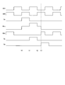
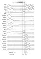
- 6 is a timing chart for explaining basic operations of the first unit circuit in the first embodiment. 6 is a timing chart for explaining a basic operation of a second unit circuit in the first embodiment. 4 is a timing chart for explaining an operation when a halfway stop of scanning is performed in the first embodiment.
- 5 is a timing chart showing a waveform of an output signal when scanning is stopped halfway in the first embodiment. 5 is a timing chart for explaining the driving of the shift register when it is desired to provide two touch processing periods in one frame period (one vertical scanning period) in the first embodiment.
- the 2nd Embodiment of this invention it is a block diagram which shows the structure of the shift register in a gate driver.
- FIG. 6 is a block diagram showing a configuration of a shift register in a gate driver in the second embodiment. It is a circuit diagram which shows the structure of the 1st unit circuit in the said 2nd Embodiment. It is a circuit diagram which shows the structure of the 2nd unit circuit in the said 2nd Embodiment. 10 is a timing chart for explaining an operation when a scan is stopped halfway in the second embodiment. It is FIG. 9 of Japanese Unexamined Patent Publication No. 2014-182203. It is FIG. 10 of Japanese Unexamined Patent Publication No. 2014-182203.
- the gate terminal (gate electrode) of the thin film transistor corresponds to the control terminal
- the drain terminal (drain electrode) corresponds to the first conduction terminal
- the source terminal (source electrode) corresponds to the second conduction terminal.
- a high level corresponds to an on level
- a low level corresponds to an off level.
- the higher of the drain and the source is called the drain, but in the description of this specification, one is defined as the drain and the other is defined as the source. May be higher.
- FIG. 2 is a block diagram showing the overall configuration of the active matrix liquid crystal display device according to the first embodiment of the present invention.
- the liquid crystal display device includes a display control circuit 100, a source driver (video signal line driving circuit) 200, a gate driver (scanning signal line driving circuit) 300, a common electrode driving circuit 400, and a display unit 500.
- the gate driver 300 and the display unit 500 are formed on the same substrate (TFT substrate which is one of the two substrates constituting the liquid crystal panel). That is, the gate driver 300 in this embodiment is a monolithic gate driver.
- TFT substrate which is one of the two substrates constituting the liquid crystal panel.
- the gate driver 300 in this embodiment is a monolithic gate driver.
- the display unit 500 includes a plurality (j) of source bus lines (video signal lines) SL1 to SLj and a plurality (i) of gate bus lines (scanning signal lines) GL1 to GLi. .
- a pixel forming portion 5 for forming pixels is provided corresponding to each intersection of the source bus lines SL1 to SLj and the gate bus lines GL1 to GLj.
- the display unit 500 includes a plurality (i ⁇ j) of pixel forming units 5.
- the plurality of pixel forming portions 5 are arranged in a matrix and constitute an i row ⁇ j column pixel matrix (pixel array).
- the symbol GL is used when it is not necessary to specify a row.
- Each pixel forming portion 5 has a thin film transistor (TFT) which is a switching element having a gate terminal connected to a gate bus line GL passing through a corresponding intersection and a source terminal connected to a source bus line SL passing through the intersection.
- TFT thin film transistor
- the pixel electrode 51 connected to the drain terminal of the thin film transistor 50
- the common electrode 54 and the auxiliary capacitance electrode 55 provided in common to the plurality of pixel forming portions 5, and the pixel electrode 51 and the common electrode 54
- the liquid crystal capacitor 52 and the auxiliary capacitor 53 constitute a pixel capacitor 56. Note that only the components corresponding to one pixel forming portion 5 are shown in the display portion 500 in FIG.
- a configuration in which at least a part of the gate driver 300 is provided in the pixel array (in the display unit 500) may be employed.
- the occurrence of waveform rounding of the scanning signal applied to the gate bus lines GL1 to GLj is suppressed, and the gate bus lines GL1 to GLj can be driven at high speed.
- all the thin film transistors 50 in the pixel forming portion 5 are n-channel type.
- the thin film transistor 50 employs an oxide TFT (a thin film transistor using an oxide semiconductor for a channel layer). Further, in this embodiment, a channel etch type is adopted for the structure of the thin film transistor 50. However, an etch stop type can also be adopted. The same applies to the thin film transistors in the gate driver 300.
- the channel etch type and the etch stop type will be described.
- the etch stop layer is not formed on the channel region, and the lower surface of the end of the source electrode and the drain electrode on the channel side is an oxide semiconductor layer. It arrange
- a channel etch type TFT is formed, for example, by forming a conductive film for a source / drain electrode on an oxide semiconductor layer and performing source / drain separation. In the source / drain separation step, the surface portion of the channel region may be etched.
- the lower surfaces of the end portions on the channel side of the source electrode and the drain electrode are located on the etch stop layer, for example.
- a conductive film for a source / drain electrode is formed on the oxide semiconductor layer and the etch stop layer.
- the oxide semiconductor included in the oxide semiconductor layer may be an amorphous oxide semiconductor or a crystalline oxide semiconductor having a crystalline portion.
- Examples of the crystalline oxide semiconductor include a polycrystalline oxide semiconductor, a microcrystalline oxide semiconductor, and a crystalline oxide semiconductor in which the c-axis is oriented substantially perpendicular to the layer surface.
- the oxide semiconductor layer may have a stacked structure of two or more layers.
- the oxide semiconductor layer may include an amorphous oxide semiconductor layer and a crystalline oxide semiconductor layer.
- the oxide semiconductor layer may include a plurality of crystalline oxide semiconductor layers having different crystal structures.
- the oxide semiconductor layer may include a plurality of amorphous oxide semiconductor layers.
- the energy gap of the oxide semiconductor included in the upper layer is preferably larger than the energy gap of the oxide semiconductor included in the lower layer.
- the energy gap of the lower oxide semiconductor may be larger than the energy gap of the upper oxide semiconductor.
- Japanese Unexamined Patent Application Publication No. 2014-007399 discloses a material, a structure, a film formation method, a structure of an oxide semiconductor layer having a stacked structure, and the like of the amorphous oxide semiconductor and each crystalline oxide semiconductor described above. Are listed.
- the oxide semiconductor layer may contain at least one metal element of In (indium), Ga (gallium), and Zn (zinc), for example.
- the oxide semiconductor layer includes, for example, an In—Ga—Zn—O-based semiconductor (eg, indium gallium zinc oxide).
- the In—Ga—Zn—O-based semiconductor is a ternary oxide of In, Ga, and Zn.
- Such an oxide semiconductor layer can be formed using an oxide semiconductor film containing an In—Ga—Zn—O-based semiconductor.
- a channel-etch TFT having an active layer containing an oxide semiconductor (OS) such as an In—Ga—Zn—O-based semiconductor may be referred to as a “CE-OS-TFT”.
- the In—Ga—Zn—O-based semiconductor may be amorphous or crystalline.
- a crystalline In—Ga—Zn—O-based semiconductor with a c-axis oriented substantially perpendicular to the layer surface is preferably used.
- the crystal structure of a crystalline In—Ga—Zn—O-based semiconductor is, for example, Japanese Unexamined Patent Publication No. 2014-007399, Japanese Unexamined Patent Publication No. 2012-134475, Japanese Unexamined Patent Publication No. 2014-209727. And the like.
- a TFT having an In—Ga—Zn—O-based semiconductor layer has high mobility (mobility more than 20 times that of an a-Si TFT) and low leakage current (leakage less than 1/100 of that of an a-Si TFT). Therefore, it is suitably used as a driving TFT (for example, a thin film transistor in the gate driver 300) and a pixel TFT (the thin film transistor 50).
- the oxide semiconductor layer may include another oxide semiconductor instead of the In—Ga—Zn—O-based semiconductor.
- the oxide semiconductor layer may include, for example, an In—Sn—Zn—O-based semiconductor (eg, In 2 O 3 —SnO 2 —ZnO; InSnZnO).
- the In—Sn—Zn—O-based semiconductor is a ternary oxide of In (indium), Sn (tin), and Zn (zinc).
- the oxide semiconductor layer includes an In—Al—Zn—O based semiconductor, an In—Al—Sn—Zn—O based semiconductor, a Zn—O based semiconductor, an In—Zn—O based semiconductor, and a Zn—Ti—O based semiconductor.
- Cd—Ge—O based semiconductor Cd—Pb—O based semiconductor, CdO (cadmium oxide), Mg—Zn—O based semiconductor, In—Ga—Sn—O based semiconductor, In—Ga—O based semiconductor, A Zr—In—Zn—O based semiconductor, an Hf—In—Zn—O based semiconductor, or the like may be included.
- the display control circuit 100 receives an image signal DAT and a timing signal group TG such as a horizontal synchronization signal and a vertical synchronization signal sent from the outside, and operates the digital video signal DV and the operation of the source driver 200.
- a source control signal SCTL for controlling and a gate control signal GCTL for controlling the operation of the gate driver 300 are output.
- the source control signal SCTL includes a source start pulse signal, a source clock signal, and a latch strobe signal.
- the gate control signal GCTL will be described later.
- the source driver 200 receives the digital video signal DV and the source control signal SCTL output from the display control circuit 100, and applies driving video signals to the source bus lines SL1 to SLj. At this time, the source driver 200 sequentially holds the digital video signal DV indicating the voltage to be applied to each source bus line SL at the timing when the pulse of the source clock signal is generated. The held digital video signal DV is converted into an analog voltage at the timing when the pulse of the latch strobe signal is generated. The converted analog voltage is simultaneously applied to all the source bus lines SL as a driving video signal.
- the gate driver 300 Based on the gate control signal GCTL output from the display control circuit 100, the gate driver 300 sequentially applies active scanning signals one by one to the gate bus lines GL1 to GLi (selects one by one sequentially). ). That is, the gate driver 300 scans the gate bus line GL. At that time, scanning is stopped halfway at a predetermined timing. A detailed description of the gate driver 300 will be described later.
- the common electrode drive circuit 400 gives a predetermined potential Vcom to the common electrode 54c.
- the driving video signals are applied to the source bus lines SL1 to SLj, the scanning signals are applied to the gate bus lines GL1 to GLi, and the predetermined potential Vcom is applied to the common electrode 54.
- An image based on the image signal DAT sent from the outside is displayed on the display unit 500.
- the gate driver 300 includes a shift register 310 having a plurality of stages.
- the shift register 310 includes a first unit circuit UCa that is a unit circuit connected to the gate bus line GL and a second unit that is a unit circuit not connected to the gate bus line GL. Circuit UCb.
- the scan of the gate bus line GL is sequentially performed row by row from the first row to the i-th row.
- the second unit circuit UCb is provided in order to make it possible to stop such scanning halfway.
- the first unit circuit UCa corresponding to the 50th row gate bus line GL50 is used.
- a second unit circuit UCb is provided between the first unit circuit UCa and the first unit circuit UCa.
- the gate driver 300 includes two gate start pulse signals GSP1, GSP2, four gate clock signals CLK1, CLK1B, CLK2, and CLK2B, and three signals CLR, CLRL and RSM and a low-level power supply voltage VSS are applied. Note that the magnitude of the potential applied based on the low-level power supply voltage VSS is referred to as “VSS potential” for convenience.
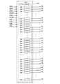
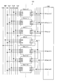
- FIG. 4 and 5 are block diagrams showing the configuration of the shift register 310 in the gate driver 300 in the present embodiment. Here, it is assumed that scanning is stopped halfway after selection of the nth gate bus line GLn.
- FIG. 4 is a diagram for explaining the configuration of the first unit circuit UCa arranged outside the vicinity of the second unit circuit UCb
- FIG. 5 shows the second unit circuit UCb and the second unit circuit UCb. It is a figure for demonstrating the structure of 1st unit circuit UCa arrange
- FIG. 4 shows first unit circuits UCa (1) to UCa (4) corresponding to the gate bus lines GL1 to GL4 from the first row to the fourth row.
- FIG. 5 shows the first unit circuit UCa (n-2) corresponding to the gate bus lines GLn-2 to GLn from the second unit circuit UCb (n), (n-2) th row to the nth row.
- the first unit circuit UCa has an input terminal for receiving a first clock signal CKA and a second clock signal CKB, which are two-phase clock signals, and a low-level power source.
- An input terminal for receiving the voltage VSS, an input terminal for receiving the set signal Sa, an input terminal for receiving the reset signal Ra, and an output terminal for outputting the output signal (shift pulse) Qa are provided. ing.
- the signals given to the input terminals of the first unit circuits UCa will be described. Note that the low-level power supply voltage VSS is commonly applied to all the first unit circuits UCa (1) to UCa (i).
- the first clock signal CKA and the second clock signal CKB are given to the first unit circuit UCa as follows.
- the gate clock signal CLK1 is supplied as the first clock signal CKA
- the gate clock signal CLK1B is supplied as the second clock signal CKB.
- the gate clock signal CLK2 is supplied as the first clock signal CKA
- the gate clock signal CLK2B is supplied as the second clock signal CKB.
- the gate clock signal CLK1B is supplied as the first clock signal CKA
- the gate clock signal CLK1 is supplied as the second clock signal CKB.
- the gate clock signal CLK2B is supplied as the first clock signal CKA
- the gate clock signal CLK2 is supplied as the second clock signal CKB.
- the set signal Sa is given to the first unit circuit UCa as follows (see FIG. 6). Focusing on the first unit circuit UCa (k) corresponding to the gate bus line GLk in the k-th row (k is an integer between 1 and i), the first unit circuit UCa (k ⁇ 2) in the previous two stages The output signal Qa (k-2) from) is given as the set signal Sa. However, the gate start pulse signal GSP1 is given as the set signal Sa for the first unit circuit UCa (1), and the gate start pulse signal GSP2 is given as the set signal Sa for the first unit circuit UCa (2).
- the output signal Qb (n) from the second unit circuit UCb (n) is given as the set signal Sa.
- the first unit circuit UCa (2) may have a configuration in which the gate start pulse signal GSP1 is given as the set signal Sa instead of the gate start pulse signal GSP2.
- the reset signal Ra is given to the first unit circuit UCa as follows (see FIG. 6). Focusing on the first unit circuit UCa (k) corresponding to the k-th gate bus line GLk, the output signal Qa (k + 3) from the first unit circuit UCa (k + 3) after the third stage is used as the reset signal Ra. Given. However, the first unit circuit UCa (n-2), the first unit circuit UCa (n-1), the first unit circuit UCa (n), the first unit circuit UCa (i-2), the first For the unit circuit UCa (i ⁇ 1) and the first unit circuit UCa (i), the signal CLR is supplied as the reset signal Ra.
- the signal CLRL is given as the reset signal Rb
- the gate clock signal CLK1 is given as the control signal Z
- the output signal Qa (n) from the first unit circuit UCa (n) is given as the set signal Sb
- the signal RSM And a low-level power supply voltage VSS is applied.
- an output signal from the second unit circuit UCb may be given to the touch panel, and the output signal may be used for processing on the touch panel. As a result, the output signal from the second unit circuit UCb can be efficiently used.
- FIG. 7 is a circuit diagram showing a configuration of the first unit circuit UCa in the present embodiment.
- the first unit circuit UCa includes seven thin film transistors T1a to T7a and one capacitor C1a.
- the first unit circuit UCa has four input terminals 61 to 64 and one output terminal 69 in addition to the input terminal for the low-level power supply voltage VSS.
- An input terminal that receives the set signal Sa is denoted by reference numeral 61
- an input terminal that receives the reset signal Ra is denoted by reference numeral 62
- an input terminal that receives the first clock signal CKA is denoted by reference numeral 63
- the input terminal that receives the 2-clock signal CKB is denoted by reference numeral 64.
- An output terminal for outputting the output signal Qa is denoted by reference numeral 69.
- the source terminal of the thin film transistor T1a, the drain terminal of the thin film transistor T2a, the gate terminal of the thin film transistor T3a, the drain terminal of the thin film transistor T4a, and the gate terminal of the thin film transistor T6a are connected to each other.
- the internal node where these are connected to each other is denoted by reference numeral N1a.
- the gate terminal of the thin film transistor T4a, the source terminal of the thin film transistor T5a, and the drain terminal of the thin film transistor T6a are connected to each other.
- An internal node where these are connected to each other is denoted by reference numeral N2a.
- the gate terminal and the drain terminal are connected to the input terminal 61 (that is, diode connection), and the source terminal is connected to the internal node N1a.
- the gate terminal is connected to the input terminal 62
- the drain terminal is connected to the internal node N1a
- the source terminal is connected to the input terminal for the power supply voltage VSS.
- the gate terminal is connected to the internal node N1a
- the drain terminal is connected to the input terminal 63
- the source terminal is connected to the output terminal 69.
- the gate terminal is connected to the node N2a, the drain terminal is connected to the internal node N1a, and the source terminal is connected to the input terminal for the power supply voltage VSS.
- the gate terminal and the drain terminal are connected to the input terminal 64 (that is, diode connection), and the source terminal is connected to the node N2a.
- the gate terminal is connected to the internal node N1a, the drain terminal is connected to the node N2a, and the source terminal is connected to the input terminal for the power supply voltage VSS.
- the gate terminal is connected to the input terminal 64, the drain terminal is connected to the output terminal 69, and the source terminal is connected to the input terminal for the power supply voltage VSS.
- the capacitor C1a has one end connected to the internal node N1a and the other end connected to the output terminal 69.
- the thin film transistor T1a changes the potential of the internal node N1a toward the high level when the set signal Sa is at the high level.
- the thin film transistor T2a changes the potential of the internal node N1a toward the VSS potential when the reset signal Ra is at a high level.
- the thin film transistor T3a applies the potential of the first clock signal CKA to the output terminal 69 when the potential of the internal node N1a is at a high level.
- the thin film transistor T4a changes the potential of the internal node N1a toward the VSS potential when the potential of the internal node N2a is at a high level.
- the thin film transistor T5a changes the potential of the internal node N2a toward the high level when the second clock signal CKB is at the high level.
- the thin film transistor T6a changes the potential of the internal node N2a toward the VSS potential when the potential of the internal node N1a is at a high level.
- the thin film transistor T7a changes the potential of the output signal Qa (the potential of the output terminal 69) toward the VSS potential when the second clock signal CKB is at a high level.
- Capacitor C1a functions as a bootstrap capacitor for increasing the potential of internal node N1a as the potential of output terminal 69 increases.
- first output control node stabilizing unit 312a for maintaining the level is realized.
- the configuration of the first output control node stabilizing unit 312a shown in FIG. 7 is an example, and the present invention is not limited to this.
- the thin film transistor T7a realizes a circuit 314a (hereinafter referred to as “first output node stabilizing section”) 314a for maintaining the potential of the output signal Qa (the potential of the output terminal 69) at a low level throughout the non-selection period. Yes.
- first output node stabilizing section a circuit 314a (hereinafter referred to as “first output node stabilizing section”) 314a for maintaining the potential of the output signal Qa (the potential of the output terminal 69) at a low level throughout the non-selection period.
- the first output control node turn-on transistor is realized by the thin film transistor T1a
- the first output control node turn-off transistor is realized by the thin film transistor T2a
- the first output control transistor is realized by the thin film transistor T3a.
- the first capacitance is realized by the capacitor C1a.
- the output terminal 69 implements a first output node
- the internal node N1a implements a first output control node.
- FIG. 8 is a circuit diagram showing a configuration of the second unit circuit UCb in the present embodiment.
- the second unit circuit UCb includes seven thin film transistors T1b to T7b and one capacitor C1b.
- the second unit circuit UCb has four input terminals 71 to 74 and one output terminal 79 in addition to the input terminal for the low-level power supply voltage VSS.
- the input terminal that receives the set signal Sb is denoted by reference numeral 71
- the input terminal that receives the reset signal Rb is denoted by reference numeral 72
- the input terminal that receives the signal RSM is denoted by reference numeral 73
- the control signal Z is assigned.
- the receiving input terminal is denoted by reference numeral 74.
- reference numeral 79 is attached to an output terminal for outputting the output signal Qb.
- the source terminal of the thin film transistor T1b, the drain terminal of the thin film transistor T2b, the gate terminal of the thin film transistor T3b, the drain terminal of the thin film transistor T4b, and the gate terminal of the thin film transistor T6b are connected to each other.
- An internal node where these are connected to each other is denoted by reference numeral N1b.
- the gate terminal of the thin film transistor T4b, the source terminal of the thin film transistor T5b, and the drain terminal of the thin film transistor T6b are connected to each other.
- An internal node where these are connected to each other is denoted by reference numeral N2b.
- the gate terminal and the drain terminal are connected to the input terminal 71 (that is, diode connection), and the source terminal is connected to the internal node N1b.
- the gate terminal is connected to the input terminal 72
- the drain terminal is connected to the internal node N1b
- the source terminal is connected to the input terminal for the power supply voltage VSS.
- the gate terminal is connected to the internal node N1b
- the drain terminal is connected to the input terminal 73
- the source terminal is connected to the output terminal 79.
- the gate terminal is connected to the node N2b, the drain terminal is connected to the internal node N1b, and the source terminal is connected to the input terminal for the power supply voltage VSS.
- the gate terminal and the drain terminal are connected to the input terminal 74 (that is, diode connection), and the source terminal is connected to the node N2b.
- the gate terminal is connected to the internal node N1b, the drain terminal is connected to the node N2b, and the source terminal is connected to the input terminal for the power supply voltage VSS.
- the gate terminal is connected to the input terminal 74, the drain terminal is connected to the output terminal 79, and the source terminal is connected to the input terminal for the power supply voltage VSS.
- One end of the capacitor C1b is connected to the internal node N1b, and the other end is connected to the output terminal 79.
- the thin film transistor T1b changes the potential of the internal node N1b toward the high level when the set signal Sb is at the high level.
- the thin film transistor T2b changes the potential of the internal node N1b toward the VSS potential when the reset signal Ra is at a high level.
- the thin film transistor T3b applies the potential of the signal RSM to the output terminal 79 when the potential of the internal node N1b is at a high level.
- the thin film transistor T4b changes the potential of the internal node N1b toward the VSS potential when the potential of the internal node N2b is at a high level.
- the thin film transistor T5b changes the potential of the internal node N2b toward the high level when the control signal Z is at the high level.
- the thin film transistor T6b changes the potential of the internal node N2b toward the VSS potential when the potential of the internal node N1b is at a high level.
- the thin film transistor T7b changes the potential of the output signal Qb (the potential of the output terminal 79) toward the VSS potential when the control signal Z is at a high level.
- Capacitor C1b functions as a bootstrap capacitor for increasing the potential of internal node N1b as the potential of output terminal 79 increases.
- the thin film transistor T4b, the thin film transistor T5b, and the thin film transistor T6b is a circuit for maintaining the potential of the node N1b at a low level throughout a period other than a touch processing period described later (except for a period just before the touch processing period).
- a “second output control node stabilizing unit” 312b is realized.
- the configuration of the second output control node stabilizing unit 312b illustrated in FIG. 8 is an example, and the present invention is not limited to this.
- second output node stabilizing unit 314b a circuit for maintaining the potential of the output signal Qb (the potential of the output terminal 79) at a low level throughout the period other than the period before the end of the touch processing period by the thin film transistor T7b (hereinafter referred to as “second output node stabilizing unit”). 314b) is realized.
- the configuration of the second output node stabilizing unit 314b illustrated in FIG. 8 is an example, and the present invention is not limited to this.
- the second output control node turn-on transistor is realized by the thin film transistor T1b
- the second output control node turn-off transistor is realized by the thin film transistor T2b
- the second output control transistor is realized by the thin film transistor T3b.
- a second capacitance is realized by the capacitor C1b.
- the output terminal 79 implements a second output node
- the internal node N1b implements a second output control node.
- FIG. 9 is a timing chart for explaining the basic operation of the first unit circuit UCa.
- FIG. 10 is a timing chart for explaining the basic operation of the second unit circuit UCb.
- FIG. 11 is a timing chart for explaining the operation when the scanning is stopped halfway.
- FIG. 12 is a timing chart showing waveforms of the output signals Qa and Qb when scanning is stopped halfway.
- FIG. 13 is a timing chart for explaining the driving of the shift register when it is desired to provide two touch processing periods in one frame period (one vertical scanning period).
- the first clock signal CKA changes from the low level to the high level.
- the thin film transistor T3a since the thin film transistor T3a is in an on state, the potential of the output terminal 69 increases as the potential of the input terminal 63 increases.
- the capacitor C1a is provided between the internal node N1a and the output terminal 69, the potential of the internal node N1a increases as the potential of the output terminal 69 increases (the internal node N1a is boosted). State).
- a large voltage is applied to the thin film transistor T3a, and the potential of the output signal Qa rises to the high level potential of the first clock signal CKA.
- the gate bus line GL connected to the output terminal 69 of the first unit circuit UCa is selected.
- the set signal Sa changes from the high level to the low level at time t1.
- the thin film transistor T1a is turned off. The turning off of the thin film transistor T1a does not affect the potential of the internal node N1a.
- the first clock signal CKA changes from the high level to the low level.
- the potential of the output terminal 69 decreases as the potential of the input terminal 63 decreases, and the potential of the internal node N1a also decreases via the capacitor C1a.
- the second clock signal CKB changes from the low level to the high level. Thereby, the thin film transistor T7a is turned on. From the above, the potential of the output terminal 69, that is, the potential of the output signal Qa becomes low level.
- the internal node N1a since the potential of the internal node N1a is at a high level, even if the thin film transistor T5a is turned on by the second clock signal CKB being at a high level, the internal node The potential of N2a is maintained at a low level. Therefore, the potential of the internal node N1a does not fall to the low level during the period from the time point t0 to the time point t3.
- the second clock signal CKB is at the low level, so that the thin film transistor T7a is maintained in the off state. For this reason, the potential of the output signal Qa does not fall to a low level during this period.
- the potential of the internal node N2a becomes high level when the second clock signal CKB is high level. That is, the thin film transistor T4a is turned on every predetermined period.
- the potential of the internal node N1a is pulled to the VSS potential every predetermined period.
- the potential of the output terminal 69 is pulled to the VSS potential every predetermined period.
- Second Unit Circuit ⁇ 1.4.2 Operation of Second Unit Circuit>
- the gate bus line GL is scanned during the period before time t10.
- the potential of the internal node N1b and the potential of the output signal Qb are low level, and the potential of the internal node N2b is high level.
- a pulse (shift pulse) of the set signal Sb is given to the input terminal 71. Since the thin film transistor T1b is diode-connected as shown in FIG. 8, the thin film transistor T1b is turned on by the pulse of the set signal Sb, and the capacitor C1b is charged. As a result, the potential of the internal node N1b changes from the low level to the high level, and the thin film transistor T3b is turned on. Incidentally, the signal RSM is maintained at the low level during the period from the time point t10 to the time point t11. Therefore, during this period, the output signal Qb is maintained at a low level.
- the set signal Sb changes from the high level to the low level.
- the thin film transistor T1b is turned off.
- the signal RSM is maintained at the low level. Therefore, during this period, the output signal Qb is maintained at a low level.
- the signal RSM changes from low level to high level.
- the thin film transistor T3b since the thin film transistor T3b is in the on state, the potential of the output terminal 79 increases as the potential of the input terminal 73 increases.
- the capacitor C1b since the capacitor C1b is provided between the internal node N1b and the output terminal 79, the potential of the internal node N1b increases as the potential of the output terminal 79 increases (the internal node N1b is boosted). State).
- a large voltage is applied to the thin film transistor T3b, and the potential of the output signal Qb rises to the high level potential of the signal RSM.
- the signal RSM changes from high level to low level.
- the potential of the output terminal 79 decreases as the potential of the input terminal 73 decreases, and the potential of the internal node N1b also decreases via the capacitor C1b.
- the reset signal Rb changes from the low level to the high level.
- the thin film transistor T2b is turned on.
- the potential of the internal node N1b becomes low level.
- the control signal Z changes from the low level to the high level.
- the thin film transistor T7b is turned on.
- the potential of the output signal Qb becomes low level.
- the output signal Qa (n-3) and the output signal Qa (n-2) are at the high level, and the internal nodes N1a (n-3) and N1a (n-2) ), The potentials of the internal node N1a (n ⁇ 1) and the internal node N1a (n) are at a high level.
- the gate clock signal CLK1 changes from high level to low level, and the gate clock signal CLK1B changes from low level to high level.
- the output signal Qa (n-3) becomes low level and the output signal Qa (n-1) becomes high level.
- the gate clock signal CLK2 changes from high level to low level
- the gate clock signal CLK2B changes from low level to high level.
- the output signal Qa (n-2) becomes low level
- the output signal Qa (n) becomes high level.
- the output signal Qa (n) is given to the first unit circuit UCa (n-3) as the reset signal Ra
- the potential of the internal node N1a (n-3) becomes low level.
- the output signal Qa (n) is given to the second unit circuit UCb (n) as the set signal Sb, the potential of the internal node N1b (n) becomes high level.
- the gate clock signal CLK1B changes from the high level to the low level. As a result, the output signal Qa (n ⁇ 1) becomes low level. At time t22, the gate clock signal CLK1 is maintained at a low level.
- the gate clock signal CLK2B changes from the high level to the low level.
- the output signal Qa (n) becomes low level.
- the signal CLR changes from the low level to the high level.
- the signal CLR is supplied as a reset signal Ra to the first unit circuit UCa (n-2), the first unit circuit UCa (n-1), and the first unit circuit UCa (n).
- the potentials of the internal node N1a (n-2), the internal node N1a (n-1), and the internal node N1a (n) become low level. In this way, at time t23, scanning of the gate bus line GL is stopped.
- the signal CLR changes from high level to low level.
- the change in the level of the signal CLR at time t24 does not affect the operation of the first unit circuit UCa.
- the signal RSM changes from low level to high level.
- the internal node N1b (n) is in the boost state, and the output signal Qb (n) is at the high level. Since the output signal Qb (n) is supplied as the set signal Sa to the first unit circuit UCa (n + 1) and the first unit circuit UCa (n + 2), the potentials of the internal node N1a (n + 1) and the internal node N1a (n + 2) becomes high level.
- the signal RSM changes from high level to low level
- the signal CLRL changes from low level to high level.
- the output signal Qb (n) becomes low level
- the potential of the internal node N1b (n) becomes low level.
- the gate clock signal CLK1 changes from the low level to the high level.
- the internal node N1a (n + 1) is in the boost state, and the output signal Qa (n + 1) is at the high level.
- the signal CLRL becomes low level at time t28.
- the gate clock signal CLK2 changes from the low level to the high level.
- the internal node N1a (n + 2) is in a boost state, and the output signal Qa (n + 2) is at a high level. In this way, scanning of the gate bus line GL is resumed.
- the signal CLR is set to the high level at the time when the touch processing period should be started,
- the clock operation of the gate clock signal may be stopped throughout the period to be the touch processing period.
- the signal RSM is set to a high level slightly before the time point at which the touch processing period should end
- the signal CLRL is set to a high level at the time point at which the touch processing period should end
- the gate clock signal The clock operation may be resumed.
- the shift operation stop step is realized by the operation at time t23
- the shift operation restart step is realized by the operations at time t25 and time t26.
- the first unit circuit UCa and the second unit circuit UCb have different input signals but the same circuit configuration.
- the first unit circuit UCa and the second unit circuit UCb only the first unit circuit UCa is connected to the gate bus line GL (see FIG. 1). Therefore, the first unit circuit UCa needs to drive a larger load than the second unit circuit UCb.
- the sizes of the thin film transistor T1a, the thin film transistor T2a, the thin film transistor T3a, the thin film transistor T1b, the thin film transistor T2b, and the thin film transistor T3b are respectively S (T1a), S (T2a), S (T3a), S (T1b), S (T2b), and This is represented by S (T3b).
- the shift register 310 is a second unit circuit having a configuration similar to that of the conventional unit circuit (first unit circuit UCa) as a unit circuit for enabling a halfway stop of scanning.
- Unit circuit UCb is provided.
- the signal RSM and the signal CLRL are necessary for the operation of the second unit circuit UCb. In this way, it is possible to stop scanning halfway only by providing two new signals as compared with the conventional case.
- threshold shift between a transistor in a unit circuit arranged at a position where scanning is stopped and a transistor in another unit circuit is performed. Display failure occurs due to the difference in the size of.
- the second unit circuit UCb since the internal node N1b of the second unit circuit UCb is maintained at a high level while scanning is stopped, a large threshold shift occurs in the thin film transistor Tb3.
- the second unit circuit UCb It is not connected to the bus line GL. For this reason, the large threshold shift generated in the thin film transistor Tb3 does not affect the display quality.
- a shift register capable of stopping scanning halfway without causing a display defect is realized.
- the first unit circuit UCa is provided with the first output control node stabilizing unit 312a for maintaining the potential of the node N1a at a low level throughout the non-selection period.
- the unit circuit UCb is provided with a second output control node stabilizing unit 312b for maintaining the potential of the node N1b at a low level throughout a period other than the touch processing period (except for a period just before the touch processing period). It has been. For this reason, even if noise is mixed in the node N1a and the node N1b, the occurrence of abnormal operation due to the noise is suppressed.
- the first unit circuit UCa has the first output node stabilizing unit 314a for maintaining the potential of the output signal Qa (the potential of the output terminal 69) at a low level throughout the non-selection period.
- the second unit circuit UCb includes a second output node for maintaining the potential of the output signal Qb (the potential of the output terminal 79) at a low level throughout a period other than the period before the end of the touch processing period.
- a stabilizing portion 314b is provided. For this reason, even if noise is mixed in the output terminal 69 or the output terminal 79, the occurrence of abnormal operation due to the noise is suppressed.
- Second Embodiment> A second embodiment of the present invention will be described. The overall configuration and operation outline are the same as those in the first embodiment, and a description thereof will be omitted (see FIG. 2). Also in this embodiment, it is assumed that the liquid crystal panel constituting the display unit 500 is integrated with the touch panel.
- the gate driver 300 is configured by a shift register 310 having a plurality of stages, and the shift register 310 is a first circuit that is a unit circuit connected to the gate bus line GL.
- Unit circuit UCa and a second unit circuit UCb which is a unit circuit not connected to the gate bus line GL (see FIG. 1).
- FIG. 14 and 15 are block diagrams showing the configuration of the shift register 310 in the gate driver 300 in the present embodiment.
- FIG. 14 is a diagram for explaining the configuration of the first unit circuit UCa arranged outside the vicinity of the second unit circuit UCb.
- FIG. 15 shows the second unit circuit UCb and the second unit circuit UCb. It is a figure for demonstrating the structure of 1st unit circuit UCa arrange
- the first unit circuit UCa is provided with an input terminal for receiving the signal CLR in addition to the input terminal provided in the first embodiment.
- the second unit circuit UCb is provided with an input terminal for receiving the signal CLRL in addition to the input terminal provided in the first embodiment.
- FIG. 16 is a circuit diagram showing a configuration of the first unit circuit UCa in the present embodiment.
- the first unit circuit UCa is provided with a thin film transistor T8a, a thin film transistor T9a, a thin film transistor T10a, and an input terminal 65 in addition to the components in the first embodiment.
- a signal CLR is given to the input terminal 65.
- the gate terminal is connected to the input terminal 65, the drain terminal is connected to the internal node N1a, and the source terminal is connected to the input terminal for the power supply voltage VSS.
- the gate terminal is connected to the input terminal 65, the drain terminal is connected to the output terminal 69, and the source terminal is connected to the input terminal for the power supply voltage VSS.
- the gate terminal is connected to the input terminal 65, the drain terminal is connected to the internal node N2a, and the source terminal is connected to the input terminal for the power supply voltage VSS.
- the thin film transistor T8a changes the potential of the internal node N1a toward the VSS potential when the signal CLR is at a high level.
- the thin film transistor T9a changes the potential of the output signal Qa (the potential of the output terminal 69) toward the VSS potential when the signal CLR is at a high level.
- the thin film transistor T10a changes the potential of the internal node N2a toward the VSS potential when the signal CLR is at a high level.
- the first output control node stabilizing unit 312a is realized by the thin film transistor T4a, the thin film transistor T5a, the thin film transistor T6a, and the thin film transistor T10a. Further, the first output control node off maintaining transistor is realized by the thin film transistor T8a, and the first output node off maintaining transistor is realized by the thin film transistor T9a.
- FIG. 17 is a circuit diagram showing a configuration of the second unit circuit UCb in the present embodiment.
- the second unit circuit UCb is provided with a thin film transistor T8b, a thin film transistor T9b, a thin film transistor T10b, and an input terminal 75 in addition to the components in the first embodiment.
- the input terminal 75 is supplied with a signal CLRL.
- the gate terminal is connected to the input terminal 75, the drain terminal is connected to the internal node N1b, and the source terminal is connected to the input terminal for the power supply voltage VSS.
- the gate terminal is connected to the input terminal 75, the drain terminal is connected to the output terminal 79, and the source terminal is connected to the input terminal for the power supply voltage VSS.
- the gate terminal is connected to the input terminal 75, the drain terminal is connected to the internal node N2b, and the source terminal is connected to the input terminal for the power supply voltage VSS.
- the thin film transistor T8b changes the potential of the internal node N1b toward the VSS potential when the signal CLRL is at a high level.
- the thin film transistor T9b changes the potential of the output signal Qb (the potential of the output terminal 79) toward the VSS potential when the signal CLRL is at a high level.
- the thin film transistor T10b changes the potential of the internal node N2b toward the VSS potential when the signal CLRL is at a high level.
- the second output control node stabilizing unit 312b is realized by the thin film transistor T4b, the thin film transistor T5b, the thin film transistor T6b, and the thin film transistor T10b. Further, the second output control node off maintaining transistor is realized by the thin film transistor T8b, and the second output node off maintaining transistor is realized by the thin film transistor T9b.
- the signal given to the input terminal 72 and the signal given to the input terminal 75 are the same. Accordingly, the thin film transistor T8b and the input terminal 75 may be removed from the configuration shown in FIG. 17, and the gate terminal of the thin film transistor T9b and the gate terminal of the thin film transistor T10b may be connected to the input terminal 72.
- the same operation as in the first embodiment is performed except that the signal CLRL changes from the high level to the low level. Note that the change in the level of the signal CLRL at the time point t21 does not affect the operation of the second unit circuit UCb (n).
- the same operation as in the first embodiment is performed.
- the gate clock signal CLK2B changes from the high level to the low level.
- the potential of the output signal Qa (n) becomes low level.
- the signal CLR changes from the low level to the high level.
- the signal CLR is supplied as a reset signal Ra to the first unit circuit UCa (n-2), the first unit circuit UCa (n-1), and the first unit circuit UCa (n).
- the potentials of the internal node N1a (n-2), the internal node N1a (n-1), and the internal node N1a (n) become low level.
- scanning of the gate bus line GL is stopped.
- the signal CLR is supplied to all the first unit circuits UCa in the shift register 310. For this reason, at the time point t23, the thin film transistors T8a, T9a, and T10a are turned on in all the first unit circuits UCa. Thereby, in all the first unit circuits UCa, the potential of the internal node N1a, the potential of the output terminal 69, and the potential of the internal node N2a are drawn to the VSS potential.
- the signal CLR is maintained at a high level.
- the signal RSM changes from the low level to the high level.
- the output signal Qb (n) is supplied as the set signal Sa to the first unit circuit UCa (n + 1) and the first unit circuit UCa (n + 2), the potentials of the internal node N1a (n + 1) and the internal node N1a (n + 2) Becomes high level.
- the signal CLR changes from the high level to the low level at this time point t25. In this way, in the present embodiment, the signal CLR is maintained at a high level for a longer period than in the first embodiment.
- the signal RSM changes from high level to low level.
- the potential of the output signal Qb (n) becomes low level.
- the gate clock signal CLK1 changes from the low level to the high level.
- the internal node N1a (n + 1) is in the boost state, and the output signal Qa (n + 1) is at the high level.
- the signal CLRL changes from the low level to the high level. Since the signal CLRL is supplied as the reset signal Rb to the second unit circuit UCb (n), the potential of the internal node N1b (n) becomes low level.
- the signal CLRL is given to the gate terminals of the thin film transistor T8b, the thin film transistor T9b, and the thin film transistor T10b.
- the potential of the internal node N1b, the potential of the output terminal 79, and the potential of the internal node N2b are drawn to the VSS potential.
- the same operation as in the first embodiment is performed.
- the signal CLRL is maintained at a high level.
- the signal CLRL is maintained at a high level for a longer period than in the first embodiment.
- the following effects can be obtained.
- the thin film transistors T8a, T9a, and T10a are turned on in all the first unit circuits UCa in the shift register 310. For this reason, it is possible to maintain the potentials of all internal nodes and output nodes in the first unit circuit UCa at the VSS potential while the scan is stopped (when the shift operation is stopped).
- an abnormal operation for example, an abnormal operation caused when the potential of the output signal Qa is increased and the thin film transistor 50 in the pixel forming unit 5 is turned on
- the influence of noise caused by coupling of parasitic capacitance or the like occurs. Is suppressed.
- the thin film transistors T8b, T9b, and T10b are turned on in all the second unit circuits UCb in the shift register 310. Therefore, the potentials of all internal nodes and output nodes in the second unit circuit UCb can be maintained at the VSS potential during the scan period. This makes it possible to prevent an erroneous shift pulse from being output from the second unit circuit UCb to the first unit circuit UCa at the next stage during the period during which scanning is performed. As described above, according to the present embodiment, a shift register that can stop scanning halfway without causing display failure or abnormal operation is realized.
- the liquid crystal display device has been described as an example, but the present invention is not limited to this.
- the present invention can also be applied to other display devices such as an organic EL (Electro Luminescence).
- the specific configuration of the unit circuits (the first unit circuit UCa and the second unit circuit UCb) constituting the shift register 310 is not limited to the configurations shown in the above embodiments.
- the present invention is not limited to this. The present invention can also be applied when a clock signal having a number other than four phases is used as a gate clock signal.
- the touch panel processing is performed while scanning is stopped.
- the present invention is not limited to this.
- the present invention can also be applied when the period during which scanning is stopped is used for processing other than touch panel processing.
Landscapes
- Physics & Mathematics (AREA)
- Engineering & Computer Science (AREA)
- General Physics & Mathematics (AREA)
- Theoretical Computer Science (AREA)
- Nonlinear Science (AREA)
- Chemical & Material Sciences (AREA)
- Crystallography & Structural Chemistry (AREA)
- General Engineering & Computer Science (AREA)
- Optics & Photonics (AREA)
- Mathematical Physics (AREA)
- Human Computer Interaction (AREA)
- Computer Hardware Design (AREA)
- Microelectronics & Electronic Packaging (AREA)
- Geometry (AREA)
- Liquid Crystal Display Device Control (AREA)
- Control Of Indicators Other Than Cathode Ray Tubes (AREA)
Abstract
L'objectif de la présente invention est de fournir un registre à décalage avec lequel un balayage peut être interrompu à mi-chemin sans que cela crée un affichage défectueux ou produise un fonctionnement anormal. Une pluralité de circuits élémentaires, qui constituent respectivement une partie d'une pluralité de niveaux dans un registre à décalage (310), sont configurés à partir de premiers circuits élémentaires (UCa) qui sont connectés à une ligne de bus de grille (GL) et sont configurés de façon à fournir en sortie des impulsions de décalage à la ligne de bus de grille (GL) connectée et à des niveaux successifs, et des seconds circuits élémentaires (UCb) qui ne sont pas connectés à la ligne de bus de grille (GL) et sont configurés de façon à fournir en sortie des impulsions de décalage à des niveaux successifs.
Priority Applications (1)
| Application Number | Priority Date | Filing Date | Title |
|---|---|---|---|
| US15/741,917 US10296121B2 (en) | 2015-07-09 | 2016-06-29 | Shift register, display device provided with same, and shift register driving method |
Applications Claiming Priority (2)
| Application Number | Priority Date | Filing Date | Title |
|---|---|---|---|
| JP2015137656 | 2015-07-09 | ||
| JP2015-137656 | 2015-07-09 |
Publications (1)
| Publication Number | Publication Date |
|---|---|
| WO2017006815A1 true WO2017006815A1 (fr) | 2017-01-12 |
Family
ID=57685636
Family Applications (1)
| Application Number | Title | Priority Date | Filing Date |
|---|---|---|---|
| PCT/JP2016/069202 Ceased WO2017006815A1 (fr) | 2015-07-09 | 2016-06-29 | Registre à décalage, dispositif d'affichage le comportant et procédé de commande d'un registre à décalage |
Country Status (2)
| Country | Link |
|---|---|
| US (1) | US10296121B2 (fr) |
| WO (1) | WO2017006815A1 (fr) |
Cited By (8)
| Publication number | Priority date | Publication date | Assignee | Title |
|---|---|---|---|---|
| JP2020509396A (ja) * | 2017-01-22 | 2020-03-26 | 京東方科技集團股▲ふん▼有限公司Boe Technology Group Co.,Ltd. | シフトレジスター回路、goa回路及び表示装置並びにその駆動方法 |
| US10777156B2 (en) | 2017-09-01 | 2020-09-15 | Sharp Kabushiki Kaisha | Display driving device and display device having electric potential controlling circuitry |
| EP3669368A4 (fr) * | 2017-08-17 | 2021-04-21 | BOE Technology Group Co., Ltd. | Unité de registre à décalage, circuit de commande de grille et procédé de commande, et appareil d'affichage |
| EP3736815A4 (fr) * | 2018-01-02 | 2021-08-04 | Boe Technology Group Co., Ltd. | Unité de registre à décalage, circuit d'attaque de grille, dispositif d'affichage et procédé de commande |
| WO2022109920A1 (fr) * | 2020-11-26 | 2022-06-02 | 京东方科技集团股份有限公司 | Procédé d'attaque, unité d'attaque de grille et dispositif d'affichage tactile |
| US11749225B2 (en) | 2021-11-12 | 2023-09-05 | Sharp Display Technology Corporation | Scanning signal line drive circuit and display device provided with same |
| US12517613B2 (en) | 2023-10-13 | 2026-01-06 | Sharp Display Technology Corporation | Touch display device with drive circuit that suspends high level voltage to latch transistor during touch detection |
| US12535915B2 (en) | 2023-10-13 | 2026-01-27 | Sharp Display Technology Corporation | Driver, display touch panel, and controller for stopping and resuming operation of a gate driver |
Families Citing this family (7)
| Publication number | Priority date | Publication date | Assignee | Title |
|---|---|---|---|---|
| CN105405385B (zh) * | 2015-12-31 | 2019-06-07 | 京东方科技集团股份有限公司 | Goa电路、goa电路扫描方法、显示面板和显示装置 |
| CN105513522B (zh) * | 2016-01-28 | 2018-05-01 | 京东方科技集团股份有限公司 | 移位寄存器及其驱动方法、驱动电路和显示装置 |
| KR102403265B1 (ko) * | 2017-12-21 | 2022-05-30 | 삼성전자주식회사 | 게이트 구동 집적 회로 및 이의 동작 방법 |
| US11138947B2 (en) * | 2019-06-12 | 2021-10-05 | Sharp Kabushiki Kaisha | Scanning signal line drive circuit and display device provided with same |
| CN113196369A (zh) * | 2019-10-18 | 2021-07-30 | 京东方科技集团股份有限公司 | 移位寄存器单元、驱动方法、栅极驱动电路和显示装置 |
| KR102670708B1 (ko) * | 2019-12-26 | 2024-05-29 | 엘지디스플레이 주식회사 | 쉬프트 레지스터 및 이를 포함하는 터치 표시장치 |
| WO2025209094A1 (fr) * | 2024-04-03 | 2025-10-09 | 京东方科技集团股份有限公司 | Registre à décalage, circuit d'attaque de grille et dispositif d'affichage |
Citations (3)
| Publication number | Priority date | Publication date | Assignee | Title |
|---|---|---|---|---|
| WO2010050262A1 (fr) * | 2008-10-30 | 2010-05-06 | シャープ株式会社 | Circuit de registre à décalage, dispositif d’affichage et procédé de commande de circuit de registre à décalage |
| JP2013190719A (ja) * | 2012-03-15 | 2013-09-26 | Japan Display West Co Ltd | 表示装置、表示方法、および電子機器 |
| US20150317018A1 (en) * | 2014-04-30 | 2015-11-05 | Himax Technologies Limited | Shift register adaptable to a gate driver |
Family Cites Families (3)
| Publication number | Priority date | Publication date | Assignee | Title |
|---|---|---|---|---|
| JP4899327B2 (ja) * | 2005-03-15 | 2012-03-21 | カシオ計算機株式会社 | シフトレジスタ回路及びその駆動制御方法並びに駆動制御装置 |
| KR101774470B1 (ko) * | 2010-02-18 | 2017-09-04 | 가부시키가이샤 한도오따이 에네루기 켄큐쇼 | 표시 장치 및 전자 장치 |
| JP2014182203A (ja) | 2013-03-18 | 2014-09-29 | Japan Display Inc | 表示装置および電子機器 |
-
2016
- 2016-06-29 WO PCT/JP2016/069202 patent/WO2017006815A1/fr not_active Ceased
- 2016-06-29 US US15/741,917 patent/US10296121B2/en active Active
Patent Citations (3)
| Publication number | Priority date | Publication date | Assignee | Title |
|---|---|---|---|---|
| WO2010050262A1 (fr) * | 2008-10-30 | 2010-05-06 | シャープ株式会社 | Circuit de registre à décalage, dispositif d’affichage et procédé de commande de circuit de registre à décalage |
| JP2013190719A (ja) * | 2012-03-15 | 2013-09-26 | Japan Display West Co Ltd | 表示装置、表示方法、および電子機器 |
| US20150317018A1 (en) * | 2014-04-30 | 2015-11-05 | Himax Technologies Limited | Shift register adaptable to a gate driver |
Cited By (13)
| Publication number | Priority date | Publication date | Assignee | Title |
|---|---|---|---|---|
| JP2020509396A (ja) * | 2017-01-22 | 2020-03-26 | 京東方科技集團股▲ふん▼有限公司Boe Technology Group Co.,Ltd. | シフトレジスター回路、goa回路及び表示装置並びにその駆動方法 |
| JP7723466B2 (ja) | 2017-01-22 | 2025-08-14 | 京東方科技集團股▲ふん▼有限公司 | シフトレジスター回路、goa回路及び表示装置並びにその駆動方法 |
| EP3669368A4 (fr) * | 2017-08-17 | 2021-04-21 | BOE Technology Group Co., Ltd. | Unité de registre à décalage, circuit de commande de grille et procédé de commande, et appareil d'affichage |
| US11295646B2 (en) | 2017-08-17 | 2022-04-05 | Boe Technology Group Co., Ltd. | Shift-register unit, a gate-driving circuit and driving method, and a display apparatus |
| US10777156B2 (en) | 2017-09-01 | 2020-09-15 | Sharp Kabushiki Kaisha | Display driving device and display device having electric potential controlling circuitry |
| EP3736815A4 (fr) * | 2018-01-02 | 2021-08-04 | Boe Technology Group Co., Ltd. | Unité de registre à décalage, circuit d'attaque de grille, dispositif d'affichage et procédé de commande |
| CN114793462A (zh) * | 2020-11-26 | 2022-07-26 | 京东方科技集团股份有限公司 | 驱动方法、栅极驱动单元和显示触控装置 |
| US11733806B2 (en) | 2020-11-26 | 2023-08-22 | Chongqing Boe Optoelectronics Technology Co., Ltd. | Driving method, gate drive unit and display touch device |
| CN114793462B (zh) * | 2020-11-26 | 2024-01-30 | 京东方科技集团股份有限公司 | 驱动方法、栅极驱动单元和显示触控装置 |
| WO2022109920A1 (fr) * | 2020-11-26 | 2022-06-02 | 京东方科技集团股份有限公司 | Procédé d'attaque, unité d'attaque de grille et dispositif d'affichage tactile |
| US11749225B2 (en) | 2021-11-12 | 2023-09-05 | Sharp Display Technology Corporation | Scanning signal line drive circuit and display device provided with same |
| US12517613B2 (en) | 2023-10-13 | 2026-01-06 | Sharp Display Technology Corporation | Touch display device with drive circuit that suspends high level voltage to latch transistor during touch detection |
| US12535915B2 (en) | 2023-10-13 | 2026-01-27 | Sharp Display Technology Corporation | Driver, display touch panel, and controller for stopping and resuming operation of a gate driver |
Also Published As
| Publication number | Publication date |
|---|---|
| US10296121B2 (en) | 2019-05-21 |
| US20180196563A1 (en) | 2018-07-12 |
Similar Documents
| Publication | Publication Date | Title |
|---|---|---|
| WO2017006815A1 (fr) | Registre à décalage, dispositif d'affichage le comportant et procédé de commande d'un registre à décalage | |
| JP5372268B2 (ja) | 走査信号線駆動回路、それを備えた表示装置、および走査信号線の駆動方法 | |
| JP5165153B2 (ja) | 走査信号線駆動回路およびそれを備えた表示装置、ならびに走査信号線の駆動方法 | |
| JP2024105456A (ja) | シフトレジスタユニットおよびその駆動方法、ゲート駆動回路および表示装置 | |
| JP5132818B2 (ja) | 走査信号線駆動回路およびそれを備えた表示装置 | |
| US8982107B2 (en) | Scanning signal line drive circuit and display device provided with same | |
| JP5349693B2 (ja) | 走査信号線駆動回路および走査信号線の駆動方法 | |
| TWI529682B (zh) | A scanning signal line driving circuit, a display device including the same, and a driving method of a scanning signal line | |
| JP6033225B2 (ja) | 表示装置および走査信号線の駆動方法 | |
| JP5972267B2 (ja) | 液晶表示装置および補助容量線の駆動方法 | |
| WO2014092011A1 (fr) | Dispositif d'affichage et son procédé de pilotage | |
| JP2018088301A (ja) | 単位シフトレジスタ回路、シフトレジスタ回路、単位シフトレジスタ回路の制御方法及び表示装置 | |
| WO2018193912A1 (fr) | Circuit d'attaque de ligne de signal de balayage et dispositif d'affichage équipé de ce dernier | |
| JP6246976B2 (ja) | シフトレジスタ回路およびそれを備えた表示装置 | |
| WO2016047544A1 (fr) | Registre à décalage, dispositif d'affichage le comportant et procédé de commande du registre à décalage | |
| JP6615986B2 (ja) | アクティブ基板及び撮像装置 | |
| JPWO2016002644A1 (ja) | シフトレジスタおよびそれを備える表示装置 | |
| JP2023096257A (ja) | シフトレジスタならびにそれを備えた走査信号線駆動回路および表示装置 | |
| JP2023096258A (ja) | シフトレジスタならびにそれを備えた走査信号線駆動回路および表示装置 | |
| JP2026000384A (ja) | 駆動回路、及び表示装置 | |
| JP2024051334A (ja) | 走査信号線駆動回路およびそれを備えた表示装置 |
Legal Events
| Date | Code | Title | Description |
|---|---|---|---|
| 121 | Ep: the epo has been informed by wipo that ep was designated in this application |
Ref document number: 16821284 Country of ref document: EP Kind code of ref document: A1 |
|
| NENP | Non-entry into the national phase |
Ref country code: DE |
|
| NENP | Non-entry into the national phase |
Ref country code: JP |
|
| 122 | Ep: pct application non-entry in european phase |
Ref document number: 16821284 Country of ref document: EP Kind code of ref document: A1 |