WO2017009944A1 - Dispositif de capture d'image à semi-conducteur - Google Patents
Dispositif de capture d'image à semi-conducteur Download PDFInfo
- Publication number
- WO2017009944A1 WO2017009944A1 PCT/JP2015/070129 JP2015070129W WO2017009944A1 WO 2017009944 A1 WO2017009944 A1 WO 2017009944A1 JP 2015070129 W JP2015070129 W JP 2015070129W WO 2017009944 A1 WO2017009944 A1 WO 2017009944A1
- Authority
- WO
- WIPO (PCT)
- Prior art keywords
- pixel
- photoelectric conversion
- semiconductor substrate
- solid
- imaging device
- Prior art date
- Legal status (The legal status is an assumption and is not a legal conclusion. Google has not performed a legal analysis and makes no representation as to the accuracy of the status listed.)
- Ceased
Links
Images


Classifications
-
- H—ELECTRICITY
- H04—ELECTRIC COMMUNICATION TECHNIQUE
- H04N—PICTORIAL COMMUNICATION, e.g. TELEVISION
- H04N25/00—Circuitry of solid-state image sensors [SSIS]; Control thereof
- H04N25/40—Extracting pixel data from image sensors by controlling scanning circuits, e.g. by modifying the number of pixels sampled or to be sampled
- H04N25/44—Extracting pixel data from image sensors by controlling scanning circuits, e.g. by modifying the number of pixels sampled or to be sampled by partially reading an SSIS array
-
- H—ELECTRICITY
- H04—ELECTRIC COMMUNICATION TECHNIQUE
- H04N—PICTORIAL COMMUNICATION, e.g. TELEVISION
- H04N25/00—Circuitry of solid-state image sensors [SSIS]; Control thereof
- H04N25/47—Image sensors with pixel address output; Event-driven image sensors; Selection of pixels to be read out based on image data
-
- H—ELECTRICITY
- H04—ELECTRIC COMMUNICATION TECHNIQUE
- H04N—PICTORIAL COMMUNICATION, e.g. TELEVISION
- H04N25/00—Circuitry of solid-state image sensors [SSIS]; Control thereof
- H04N25/70—SSIS architectures; Circuits associated therewith
- H04N25/703—SSIS architectures incorporating pixels for producing signals other than image signals
- H04N25/707—Pixels for event detection
-
- H—ELECTRICITY
- H04—ELECTRIC COMMUNICATION TECHNIQUE
- H04N—PICTORIAL COMMUNICATION, e.g. TELEVISION
- H04N25/00—Circuitry of solid-state image sensors [SSIS]; Control thereof
- H04N25/70—SSIS architectures; Circuits associated therewith
- H04N25/76—Addressed sensors, e.g. MOS or CMOS sensors
- H04N25/77—Pixel circuitry, e.g. memories, A/D converters, pixel amplifiers, shared circuits or shared components
-
- H—ELECTRICITY
- H04—ELECTRIC COMMUNICATION TECHNIQUE
- H04N—PICTORIAL COMMUNICATION, e.g. TELEVISION
- H04N25/00—Circuitry of solid-state image sensors [SSIS]; Control thereof
- H04N25/70—SSIS architectures; Circuits associated therewith
- H04N25/79—Arrangements of circuitry being divided between different or multiple substrates, chips or circuit boards, e.g. stacked image sensors
-
- H—ELECTRICITY
- H10—SEMICONDUCTOR DEVICES; ELECTRIC SOLID-STATE DEVICES NOT OTHERWISE PROVIDED FOR
- H10F—INORGANIC SEMICONDUCTOR DEVICES SENSITIVE TO INFRARED RADIATION, LIGHT, ELECTROMAGNETIC RADIATION OF SHORTER WAVELENGTH OR CORPUSCULAR RADIATION
- H10F39/00—Integrated devices, or assemblies of multiple devices, comprising at least one element covered by group H10F30/00, e.g. radiation detectors comprising photodiode arrays
- H10F39/10—Integrated devices
- H10F39/12—Image sensors
- H10F39/18—Complementary metal-oxide-semiconductor [CMOS] image sensors; Photodiode array image sensors
-
- H—ELECTRICITY
- H10—SEMICONDUCTOR DEVICES; ELECTRIC SOLID-STATE DEVICES NOT OTHERWISE PROVIDED FOR
- H10F—INORGANIC SEMICONDUCTOR DEVICES SENSITIVE TO INFRARED RADIATION, LIGHT, ELECTROMAGNETIC RADIATION OF SHORTER WAVELENGTH OR CORPUSCULAR RADIATION
- H10F39/00—Integrated devices, or assemblies of multiple devices, comprising at least one element covered by group H10F30/00, e.g. radiation detectors comprising photodiode arrays
- H10F39/80—Constructional details of image sensors
- H10F39/802—Geometry or disposition of elements in pixels, e.g. address-lines or gate electrodes
- H10F39/8023—Disposition of the elements in pixels, e.g. smaller elements in the centre of the imager compared to larger elements at the periphery
-
- H—ELECTRICITY
- H10—SEMICONDUCTOR DEVICES; ELECTRIC SOLID-STATE DEVICES NOT OTHERWISE PROVIDED FOR
- H10F—INORGANIC SEMICONDUCTOR DEVICES SENSITIVE TO INFRARED RADIATION, LIGHT, ELECTROMAGNETIC RADIATION OF SHORTER WAVELENGTH OR CORPUSCULAR RADIATION
- H10F39/00—Integrated devices, or assemblies of multiple devices, comprising at least one element covered by group H10F30/00, e.g. radiation detectors comprising photodiode arrays
- H10F39/80—Constructional details of image sensors
- H10F39/802—Geometry or disposition of elements in pixels, e.g. address-lines or gate electrodes
- H10F39/8027—Geometry of the photosensitive area
-
- H—ELECTRICITY
- H10—SEMICONDUCTOR DEVICES; ELECTRIC SOLID-STATE DEVICES NOT OTHERWISE PROVIDED FOR
- H10F—INORGANIC SEMICONDUCTOR DEVICES SENSITIVE TO INFRARED RADIATION, LIGHT, ELECTROMAGNETIC RADIATION OF SHORTER WAVELENGTH OR CORPUSCULAR RADIATION
- H10F39/00—Integrated devices, or assemblies of multiple devices, comprising at least one element covered by group H10F30/00, e.g. radiation detectors comprising photodiode arrays
- H10F39/80—Constructional details of image sensors
- H10F39/803—Pixels having integrated switching, control, storage or amplification elements
- H10F39/8033—Photosensitive area
-
- H—ELECTRICITY
- H10—SEMICONDUCTOR DEVICES; ELECTRIC SOLID-STATE DEVICES NOT OTHERWISE PROVIDED FOR
- H10F—INORGANIC SEMICONDUCTOR DEVICES SENSITIVE TO INFRARED RADIATION, LIGHT, ELECTROMAGNETIC RADIATION OF SHORTER WAVELENGTH OR CORPUSCULAR RADIATION
- H10F39/00—Integrated devices, or assemblies of multiple devices, comprising at least one element covered by group H10F30/00, e.g. radiation detectors comprising photodiode arrays
- H10F39/80—Constructional details of image sensors
- H10F39/809—Constructional details of image sensors of hybrid image sensors
-
- H—ELECTRICITY
- H10—SEMICONDUCTOR DEVICES; ELECTRIC SOLID-STATE DEVICES NOT OTHERWISE PROVIDED FOR
- H10F—INORGANIC SEMICONDUCTOR DEVICES SENSITIVE TO INFRARED RADIATION, LIGHT, ELECTROMAGNETIC RADIATION OF SHORTER WAVELENGTH OR CORPUSCULAR RADIATION
- H10F99/00—Subject matter not provided for in other groups of this subclass
-
- H—ELECTRICITY
- H04—ELECTRIC COMMUNICATION TECHNIQUE
- H04N—PICTORIAL COMMUNICATION, e.g. TELEVISION
- H04N5/00—Details of television systems
- H04N5/14—Picture signal circuitry for video frequency region
- H04N5/144—Movement detection
-
- H—ELECTRICITY
- H10—SEMICONDUCTOR DEVICES; ELECTRIC SOLID-STATE DEVICES NOT OTHERWISE PROVIDED FOR
- H10F—INORGANIC SEMICONDUCTOR DEVICES SENSITIVE TO INFRARED RADIATION, LIGHT, ELECTROMAGNETIC RADIATION OF SHORTER WAVELENGTH OR CORPUSCULAR RADIATION
- H10F39/00—Integrated devices, or assemblies of multiple devices, comprising at least one element covered by group H10F30/00, e.g. radiation detectors comprising photodiode arrays
- H10F39/80—Constructional details of image sensors
- H10F39/805—Coatings
- H10F39/8053—Colour filters
-
- H—ELECTRICITY
- H10—SEMICONDUCTOR DEVICES; ELECTRIC SOLID-STATE DEVICES NOT OTHERWISE PROVIDED FOR
- H10F—INORGANIC SEMICONDUCTOR DEVICES SENSITIVE TO INFRARED RADIATION, LIGHT, ELECTROMAGNETIC RADIATION OF SHORTER WAVELENGTH OR CORPUSCULAR RADIATION
- H10F39/00—Integrated devices, or assemblies of multiple devices, comprising at least one element covered by group H10F30/00, e.g. radiation detectors comprising photodiode arrays
- H10F39/80—Constructional details of image sensors
- H10F39/806—Optical elements or arrangements associated with the image sensors
- H10F39/8063—Microlenses
-
- H—ELECTRICITY
- H10—SEMICONDUCTOR DEVICES; ELECTRIC SOLID-STATE DEVICES NOT OTHERWISE PROVIDED FOR
- H10F—INORGANIC SEMICONDUCTOR DEVICES SENSITIVE TO INFRARED RADIATION, LIGHT, ELECTROMAGNETIC RADIATION OF SHORTER WAVELENGTH OR CORPUSCULAR RADIATION
- H10F39/00—Integrated devices, or assemblies of multiple devices, comprising at least one element covered by group H10F30/00, e.g. radiation detectors comprising photodiode arrays
- H10F39/80—Constructional details of image sensors
- H10F39/811—Interconnections
Definitions
- the present invention relates to a solid-state imaging device.
- Non-Patent Document 1 by detecting a change in a signal in accordance with the movement of the subject, both motion detection for sequentially detecting the motion of the subject and normal shooting are compatible.
- a technique for a solid-state imaging device has been proposed.
- each pixel is provided with one photoelectric conversion element (photodiode) that photoelectrically converts incident light, and an APS (Active Pixel) that reads out a charge signal from normal imaging.
- Sensor (Sensor) readout and AER (Address Event Representation) readout for reading out a charge signal for motion detection can be performed asynchronously.
- Non-Patent Document 1 when motion is detected, a temporal change in the charge signal photoelectrically converted by the photodiode is detected, and the magnitude of the charge signal exceeds a predetermined threshold value.
- address information indicating the position of the pixel that outputs the pulse signal, that is, the pixel that detected the movement of the subject is also added to the pulse signal output by the AER readout.
- the position of the pixel where the movement of the subject is detected can be extracted at an asynchronous timing that is not related to the timing of the frame from which the charge signal is read in normal imaging. it can.
- the solid-state imaging device proposed in Non-Patent Document 1 can capture a moving subject at a higher speed than the frame rate in normal shooting.
- each pixel with a logic circuit that detects the direction in which the charge signal has changed and a logic circuit for adding address information to the pulse signal increase the number of pixels by reducing the area of the photodiode. This also makes it difficult to increase the number of pixels of the solid-state imaging device.
- a decrease in the level of the charge signal photoelectrically converted by the photodiode means that the level of the charge signal for detecting a temporal change in motion detection also decreases, and the accuracy of motion detection decreases. It also leads to that. Therefore, in order to suppress a decrease in the accuracy of motion detection, it is conceivable to further provide an amplifier circuit (amplifier) that amplifies and outputs the pulse signal, but in this case, the further provided amplifier is also included in the logic circuit. It is necessary to further reduce the area of the photodiode, and the above-described problems of deterioration in image quality in normal photographing and increase in the number of pixels of the solid-state imaging device become more remarkable.
- the present invention has been made based on the above-described problem, and in a solid-state imaging device that achieves both motion detection for sequentially detecting the motion of a subject and normal shooting, the normal detection is performed without reducing the accuracy of motion detection.
- An object of the present invention is to provide a solid-state imaging device capable of improving image quality in photographing.
- the solid-state imaging device is stacked on a first semiconductor substrate on which light is incident and a surface opposite to the surface on which light is incident on the first semiconductor substrate.
- the first charge signal generated by the corresponding one of the first photoelectric conversion elements is stored and stored on the semiconductor substrate in correspondence with each of the n first photoelectric conversion elements.
- Each of the n first readout circuits that output a signal voltage corresponding to the first charge signal as a first pixel signal and the n first readout circuits are sequentially driven to perform the first A driving circuit for outputting each of the pixel signals, the first semiconductor substrate and the front circuit;
- the m second photoelectric conversion elements that are periodically arranged on any one of the second semiconductor substrates and generate a second charge signal obtained by photoelectrically converting incident light, and the m second photoelectric conversion elements.
- M second readout circuits that sequentially output a second pixel signal representing a change in the second charge signal generated by the corresponding one of the second photoelectric conversion elements among the conversion elements;
- Each of the m second readout circuits detects a temporal change in the second charge signal generated by the corresponding one of the second photoelectric conversion elements, and determines a predetermined threshold value.
- a detection circuit that outputs an event signal indicating the changed direction when a change exceeding 1 is detected, and one second photoelectric conversion element that is disposed on the second semiconductor substrate and corresponds to the event signal
- the address information indicating the position where the A pixel signal generating circuit for outputting a pixel signal of the said n is a natural number of 2 or more, the m is a natural number of 2 or more.
- each of the m second readout circuits is disposed on the second semiconductor substrate and has a corresponding one An amplifier circuit for amplifying the second charge signal generated by the second photoelectric conversion element; and the detection circuit detects a change in the second charge signal after being amplified by the amplifier circuit. It may be detected.
- m is smaller than the n, and each of the m second photoelectric conversion elements receives light.
- Each of the n first photoelectric conversion elements may be larger than an area for receiving light.
- each of the m second photoelectric conversion elements is disposed on the second semiconductor substrate, and the n number of the n photoelectric conversion elements are arranged.
- the first photoelectric conversion elements a second charge signal obtained by photoelectric conversion of light transmitted through the corresponding p first photoelectric conversion elements is generated, and the p may be a natural number of 1 or more. .
- the circuit of the first semiconductor substrate is formed between the first semiconductor substrate and the second semiconductor substrate.
- the circuit of the first semiconductor substrate is formed between the first semiconductor substrate and the second semiconductor substrate.
- Each of the two readout circuits represents the second charge signal representing a change in the first charge signal generated by the corresponding s first photoelectric conversion elements among the n first photoelectric conversion elements.
- Each of the m second readout circuits sequentially outputs a pixel signal, and the detection circuit included in each of the m second readout circuits has a temporal characteristic of the first charge signal generated by the corresponding s first photoelectric conversion elements.
- the event signal is output, and the connection unit electrically connects the detection circuit included in each of the m second readout circuits and the corresponding s first photoelectric conversion elements,
- the s may be a natural number of 1 or more.
- the m is smaller than the n, the s is a natural number of 2 or more, and the m second readout circuits.
- Each further includes an addition circuit for adding the first charge signals generated by the corresponding s first photoelectric conversion elements, and the detection circuit is added by the addition circuit. A subsequent change in the first charge signal may be detected.
- each of the m second readout circuits is disposed on the second semiconductor substrate and is added by the addition circuit.
- an amplifier circuit that amplifies the first charge signal after being amplified, and the detection circuit may detect a change in the first charge signal after being amplified by the amplifier circuit.
- the adder circuit is disposed on the first semiconductor substrate, and the connection unit includes the m second readouts.
- the detection circuit included in each of the circuits may be electrically connected to the corresponding addition circuit.
- a solid-state imaging device that achieves both motion detection that sequentially detects the motion of a subject and normal shooting, it is possible to improve image quality in normal shooting without reducing the accuracy of motion detection.
- a solid-state imaging device can be provided.
- 1 is an overview diagram illustrating a schematic configuration of a solid-state imaging device according to a first embodiment of the present invention.
- 1 is a block diagram illustrating a schematic configuration of a solid-state imaging device according to a first embodiment of the present invention. It is the circuit diagram which showed an example of the structure of the pixel in the solid-state imaging device of the 1st Embodiment of this invention. It is the circuit diagram which showed an example of the structure of the pixel in the solid-state imaging device of the 1st Embodiment of this invention. It is the figure which showed typically an example of arrangement
- circuit diagram which showed another example of the structure of the pixel in the solid-state imaging device of the 3rd Embodiment of this invention. It is sectional drawing which showed an example of another structure of the solid-state imaging device of the 3rd Embodiment of this invention. It is the circuit diagram which showed another example of the structure of the pixel in the solid-state imaging device of the 3rd Embodiment of this invention. It is the circuit diagram which showed another example of the structure of the pixel in the solid-state imaging device of the 3rd Embodiment of this invention.
- FIG. 1 is an overview diagram showing a schematic configuration of the solid-state imaging device according to the first embodiment of the present invention.
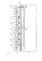
- the solid-state imaging device 1 according to the first embodiment is configured by stacking (joining) a plurality of semiconductor substrates.
- a first semiconductor substrate 11 and a second semiconductor substrate 12 are joined by a chip connection unit 13.
- the solid-state imaging device 1 forms a circuit for realizing the function of the solid-state imaging device 1 on either one of the first semiconductor substrate 11 and the second semiconductor substrate 12.
- a circuit for realizing the function of the solid-state imaging device 1 includes a pixel including a photoelectric conversion element such as a photodiode that photoelectrically converts incident light (light beam), and a readout circuit that reads a charge signal generated by the photoelectric conversion element.
- a photoelectric conversion element such as a photodiode that photoelectrically converts incident light (light beam)
- a readout circuit that reads a charge signal generated by the photoelectric conversion element.
- each circuit for realizing the function of the solid-state imaging device 1 is not only configured to be formed on one of the first semiconductor substrate 11 and the second semiconductor substrate 12 but also the first circuit.
- the semiconductor substrate 11 and the second semiconductor substrate 12 may be formed on both semiconductor substrates.
- Each circuit for realizing the function of the solid-state imaging device 1 formed on each semiconductor substrate is electrically connected by the chip connection unit 13.
- the circuit formed on the first semiconductor substrate 11 and the circuit formed on the second semiconductor substrate 12 transmit and receive signals via the chip connection portion 13.
- the chip connection portion 13 uses, for example, a micro bump produced by a vapor deposition method or a plating method.
- achieving the function of the solid-state imaging device 1 formed on each semiconductor substrate is not limited to the method using a micro bump,
- a silicon penetration electrode A method using TSV: Through-Silicon-Via may be used.
- FIG. 2 is a block diagram showing a schematic configuration of the solid-state imaging device 1 according to the first embodiment of the present invention.
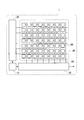
- the solid-state imaging device 1 includes a control circuit 10, a vertical scanning circuit 20, a horizontal scanning circuit 30, and a pixel array unit 40 in which a plurality of pixels 50 are arranged.
- the solid-state imaging device 1 illustrated in FIG. 1 an example of a pixel array unit 40 in which a plurality of pixels 50 are two-dimensionally arranged in 7 rows and 8 columns is illustrated.
- the control circuit 10 controls the vertical scanning circuit 20 and the horizontal scanning circuit 30.
- the vertical scanning circuit 20 is a drive circuit that controls each pixel 50 in the pixel array unit 40 in accordance with control from the control circuit 10 and outputs a pixel signal of each pixel 50 to the vertical signal line 60.
- the vertical scanning circuit 20 outputs a control signal for driving the pixels 50 for each row of the pixels 50 provided in the pixel array unit 40.
- the horizontal scanning circuit 30 is a drive circuit that sequentially outputs pixel signals output for each row from the respective pixels 50 provided in the pixel array unit 40 to the outside of the solid-state imaging device 1.
- Each pixel 50 arranged in the pixel array unit 40 generates a charge signal obtained by photoelectrically converting incident light (light beam).
- the pixels 50 arranged in the pixel array unit 40 include a pixel 50 configured to generate a charge signal by normal photographing and a pixel 50 configured to generate a charge signal for motion detection.
- the pixel 50 configured to generate a charge signal by normal photographing is generated by APS (Active Pixel Sensor) reading (hereinafter referred to as “normal reading”) in accordance with a control signal input from the vertical scanning circuit 20.
- a pixel signal corresponding to the signal is output to the vertical signal line 60 for each row.
- the pixel signals of each row output to the vertical signal line 60 are output to the outside of the solid-state imaging device 1 according to control by the horizontal scanning circuit 30. That is, the pixel signal of the pixel 50 configured to generate a charge signal by normal shooting is output to the outside of the solid-state imaging device 1 for each frame in normal shooting.
- a pixel 50 configured to generate a charge signal by normal photographing that is, a pixel 50 that outputs a normal photographing pixel signal is referred to as a “normal pixel 51”.
- the pixel 50 configured to generate a charge signal for motion detection represents a temporal change and a changed direction of the charge signal by AER (Address Event Representation) reading (hereinafter referred to as “motion detection reading”).
- the pulse signal is output without being synchronized with the driving of the normal pixel 51 by the vertical scanning circuit 20, that is, asynchronously.
- the pixel 50 configured to generate a charge signal for motion detection adds address information indicating the position of the pixel 50 itself to the pulse signal and outputs it as a pixel signal.
- a pixel 50 configured to generate a charge signal for motion detection that is, a pixel 50 that outputs a pixel signal for motion detection is referred to as a “motion detection pixel 52”.
- Circuit elements constituting each of the normal pixel 51 and the motion detection pixel 52 are formed on one or both of the first semiconductor substrate 11 and the second semiconductor substrate 12, and the pixel array is formed by the chip connection unit 13. The connection is made within the unit 40.
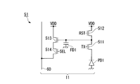
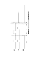
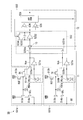
- FIG. 3A and 3B are circuit diagrams illustrating an example of the configuration of the pixel 50 (the normal pixel 51 and the motion detection pixel 52) in the solid-state imaging device 1 according to the first embodiment of the present invention.
- FIG. 3A shows an example of the configuration of the normal pixel 51 arranged in the pixel array unit 40 of the solid-state imaging device 1
- FIG. 3B shows the motion detection pixel 52 arranged in the pixel array unit 40 of the solid-state imaging device 1.
- An example of the configuration is shown.
- the normal pixel 51 includes a photoelectric conversion element PD1, a charge transfer transistor 511, a pixel reset transistor 512, an amplification transistor 513, and a selection transistor 514.
- a node capacitance FD1 which is a capacitance associated with a node connected to the gate terminal of the amplification transistor 513 provided in the normal pixel 51, is indicated by a capacitor symbol as a circuit element of the normal pixel 51.
- the charge transfer transistor 511, the pixel reset transistor 512, the amplification transistor 513, the selection transistor 514, and the node capacitor FD1 read out a pixel signal corresponding to the charge signal generated by the photoelectric conversion element PD1.
- the circuit is configured.
- the photoelectric conversion element PD ⁇ b> 1 and the readout circuit are formed on the first semiconductor substrate 11.
- the photoelectric conversion element PD1 is a photodiode that photoelectrically converts incident light (light beam) to generate a charge signal and accumulates the generated charge signal.
- the charge transfer transistor 511 transfers the charge signal generated and accumulated by the photoelectric conversion element PD1 to the gate terminal of the amplification transistor 513 in accordance with the control signal TX input from the vertical scanning circuit 20. As a result, the charge signal transferred by the charge transfer transistor 511 is accumulated in the node capacitor FD1.
- the amplification transistor 513 outputs to the selection transistor 514 a signal voltage corresponding to the charge signal transferred to the gate terminal, that is, the charge signal stored in the node capacitor FD1.
- the pixel reset transistor 512 resets the charge signal in the normal pixel 51 to the power supply voltage VDD in accordance with the control signal RST input from the vertical scanning circuit 20.
- the selection transistor 514 outputs the signal voltage output from the amplification transistor 513 to the vertical signal line 60 as the pixel signal of the normal pixel 51 in accordance with the control signal SEL input from the vertical scanning circuit 20. As a result, a pixel signal corresponding to the charge signal generated by the photoelectric conversion element PD ⁇ b> 1 provided in the normal pixel 51 is read out to the vertical signal line 60.
- each signal voltage corresponding to the charge signal obtained by photoelectrically converting the light incident on the photoelectric conversion element PD1 is read out to the vertical signal line 60 as a pixel signal.
- the motion detection pixel 52 includes a photoelectric conversion element PD2, an amplifier 521, a bias transistor 522, a switched capacitor amplifier circuit 523, a threshold amplifier 524, a threshold amplifier 525, and an AER circuit 526.
- the switched capacitor amplifier circuit 523 includes a capacitor 5231, an amplifier 5232, a capacitor 5233, and a switch 5234.
- an amplifier 521 and a bias transistor 522 constitute an output circuit that outputs a charge signal generated by the photoelectric conversion element PD2.
- the switched capacitor amplifier circuit 523, the threshold amplifier 524, the threshold amplifier 525, and the AER circuit 526 form a readout circuit that reads the charge signal generated by the photoelectric conversion element PD2.
- the photoelectric conversion element PD ⁇ b> 2 and the output circuit are formed on the first semiconductor substrate 11, and the readout circuit is formed on the second semiconductor substrate 12.
- the photoelectric conversion element PD2 is a photodiode that photoelectrically converts incident light (light rays) to generate a charge signal and accumulates the generated charge signal. .
- the photoelectric conversion element PD2 sequentially outputs the generated charge signal to the amplifier 521.
- the amplifier 521 amplifies the charge signal generated and output by the photoelectric conversion element PD2.
- the amplifier 521 outputs the amplified charge signal to the switched capacitor amplifier circuit 523 via the chip connection unit 13.
- a change in the charge signal generated by the photoelectric conversion element PD2 is input to the switched capacitor amplifier circuit 523.
- the amplifier 521 transfers the amplified charge signal to the gate terminal of the bias transistor 522.
- the bias transistor 522 controls the current flowing through the photoelectric conversion element PD2 to be a constant current according to the charge signal transferred to the gate terminal.
- the charge signal generated by the photoelectric conversion element PD2 changes, the magnitude of the charge signal is stabilized at the magnitude after the change. That is, the output of the photoelectric conversion element PD2 is clipped.
- the switched capacitor amplifier circuit 523 converts the change in the charge signal input from the amplifier 521 via the chip connection unit 13, that is, the increase or decrease in the charge signal generated by the photoelectric conversion element PD2 into a voltage signal in a predetermined voltage range.
- the data is converted and output to each of the threshold amplifier 524 and the threshold amplifier 525.
- the operation of the switched capacitor amplifier circuit 523 is reset by the AER circuit 526.
- the charge signal input from the amplifier 521 via the chip connection unit 13 is input to the first terminal of the capacitor 5231 and stored. Accordingly, a voltage signal having a voltage corresponding to the accumulated charge signal is output from the second terminal of the capacitor 5231 and output to the amplifier 5232.
- the amplifier 5232 amplifies the voltage of the input voltage signal, and outputs the amplified voltage signal as an output of the switched capacitor amplifier circuit 523 in each of the threshold amplifier 524 and the threshold amplifier 525.
- the voltage signal output from the amplifier 5232 is input to the first terminal of the capacitor 5233 and accumulated.
- a voltage signal corresponding to the accumulated voltage signal is output from the second terminal of the capacitor 5233 to the amplifier 5232 as a feedback signal.
- the amplifier 5232 continues to output a voltage signal having a constant voltage corresponding to the voltage of the feedback signal.
- the amplifier 5232 continues to output a voltage signal having a voltage corresponding to the charge signal input from the amplifier 521 to the switched capacitor amplifier circuit 523 via the chip connection unit 13 to each of the threshold amplifier 524 and the threshold amplifier 525.
- the voltage signal output from the amplifier 5232 to each of the threshold amplifier 524 and the threshold amplifier 525 is a voltage signal indicating the magnitude of increase or decrease in the charge signal generated by the photoelectric conversion element PD2.
- the output terminal of the amplifier 5232 (which is also the first terminal of the capacitor 5233) is connected to the first terminal of the switch 5234, and the input terminal of the amplifier 5232 (which is also the second terminal of the capacitor 5233) is the switch. 5234 is connected to the second terminal.
- the switch 5234 is output from the AER circuit 526, and the short circuit and the open circuit are controlled by the reset signal input to the control terminal.
- the switch 5234 When the switch 5234 is controlled to be short-circuited by the reset signal output from the AER circuit 526, the switch 5234 short-circuits the first terminal and the second terminal. Accordingly, both terminals of the capacitor 5233 are short-circuited, the voltages of both terminals of the capacitor 5233 are reset to the same voltage, and the amplification operation of the voltage signal by the amplifier 5232 is also reset.
- FIG. 3B shows the switched capacitor amplifier circuit 523 configured by the capacitor 5231, the amplifier 5232, the capacitor 5233, and the switch 5234.
- the configuration of the switched capacitor amplifier circuit 523 is limited to the configuration illustrated in FIG. 3B. It is not something.
- Each of the threshold amplifier 524 and the threshold amplifier 525 detects a change in the voltage of the voltage signal input from the amplifier 5232 in the switched capacitor amplifier circuit 523 and the changed direction.
- each of the threshold amplifier 524 and the threshold amplifier 525 compares the voltage of the voltage signal input from the amplifier 5232 in the switched capacitor amplifier circuit 523 with a predetermined threshold voltage (threshold voltage).
- a predetermined threshold voltage threshold voltage
- Each of the threshold amplifier 524 and the threshold amplifier 525 outputs an event signal indicating that there is a change exceeding the threshold voltage to the AER circuit 526 when the voltage of the input voltage signal exceeds the threshold voltage.
- the threshold amplifier 524 and the threshold amplifier 525 either a predetermined positive voltage or negative voltage is set as the threshold voltage.
- a positive voltage having a predetermined voltage value is set as a threshold voltage in the threshold amplifier 524
- a negative voltage having a predetermined voltage value is set as a threshold voltage in the threshold amplifier 525.
- the threshold amplifier 524 detects whether or not the voltage of the voltage signal input from the amplifier 5232 has changed in the positive direction (increase direction) more than the threshold voltage in the positive direction.
- the threshold amplifier 525 detects whether the voltage of the voltage signal input from the amplifier 5232 has changed in the negative direction (decreasing direction) more than the threshold voltage in the negative direction.
- the configuration of the threshold amplifier 524 and the threshold amplifier 525 detects the change exceeding the threshold voltage of the voltage signal converted into the predetermined voltage range by the switched capacitor amplifier circuit 523 and the changed direction. This corresponds to detecting a change and a changed direction of the charge signal generated by the photoelectric conversion element PD2 exceeding a predetermined threshold.
- the event signals output from the threshold amplifier 524 and the threshold amplifier 525 to the AER circuit 526 represent the change of the charge signal generated by the photoelectric conversion element PD2 and the changed direction (positive direction or negative direction).
- the threshold amplifier 524 when the threshold amplifier 524 outputs an event signal, it indicates that the charge signal generated by the photoelectric conversion element PD2 has changed beyond a predetermined threshold value in the positive direction, and the threshold amplifier 525 outputs the event signal. When output, it indicates that the charge signal generated by the photoelectric conversion element PD2 has changed beyond a predetermined threshold value in the negative direction.
- the temporal change of the charge signal generated by the photoelectric conversion element PD2 is detected by the configuration of the switched capacitor amplifier circuit 523, the threshold amplifier 524, and the threshold amplifier 525.
- the configuration for detecting the temporal change of the charge signal generated by the photoelectric conversion element PD2 is not limited to the configuration shown in FIG. 3B.
- the threshold amplifier 524 and the threshold amplifier 525 may be configured to detect temporal changes in the charge signal generated by the photoelectric conversion element PD2.
- the AER circuit 526 determines whether the charge signal generated by the photoelectric conversion element PD2 changes in the positive direction or the negative direction based on the event signals input from the threshold amplifier 524 and the threshold amplifier 525, respectively. That is, the increase / decrease in the magnitude of the charge signal is determined. Then, the AER circuit 526 generates a pulse signal representing the determined result. For example, when the charge signal generated by the photoelectric conversion element PD2 changes in the positive direction (increase direction), a positive pulse signal is generated, and the charge signal generated by the photoelectric conversion element PD2 decreases in the negative direction (decreases). Direction), a negative pulse signal is generated.
- the AER circuit 526 adds address information indicating the position of the motion detection pixel 52 itself to the generated pulse signal, and outputs it as a pixel signal.
- the pixel signal output from the AER circuit 526 that is, the motion detection pixel 52
- an “event pixel signal” in order to distinguish from the pixel signal output from the normal pixel 51.
- the motion detection pixel 52 detects a change in the charge signal obtained by photoelectric conversion of the light incident on the photoelectric conversion element PD2 and its changed direction, and detects the detected information and the position of the motion detection pixel 52.
- the address information to be expressed is output for each motion detection pixel 52.
- the event pixel signal output from the motion detection pixel 52 may be output for each motion detection pixel 52 as described above, but each motion detection pixel 52 outputs an event pixel signal.
- the configuration is not limited.
- each motion detection pixel 52 may be configured to output an event pixel signal via the horizontal scanning circuit 30.
- the structure which outputs an event pixel signal in the form put together for every predetermined range in the pixel array part 40 may be sufficient.
- the AER circuit 526 adds the address information to the generated pulse signal and outputs the event pixel signal.
- the configuration for adding the address information to the pulse signal is the AER It is not limited to the circuit 526.
- the address information indicating the position of the motion detection pixel 52 that outputs the pulse signal to the pulse signal output from the AER circuit 526 provided in each motion detection pixel 52 by a component (not shown) included in the solid-state imaging device 1. May be added and output as an event pixel signal.
- the switched capacitor amplifier circuit 523 amplifies the charge signal generated by the photoelectric conversion element PD2 and then converts the amplified signal into a voltage signal in a predetermined voltage range.
- the configuration for converting the charge signal generated by the photoelectric conversion element PD2 into a voltage signal in a predetermined voltage range is not limited to the configuration using the switched capacitor amplifier circuit 523.
- the motion detection pixel 52 is configured so as not to include the amplifier 5232 included in the switched capacitor amplifier circuit 523, that is, a so-called switched capacitor circuit, and the charge signal generated by the photoelectric conversion element PD2 is converted into a voltage signal in a predetermined voltage range. You may make it the structure to convert. In this case, the motion detection pixel 52 may detect a temporal change in the charge signal generated by the photoelectric conversion element PD2 by the configuration of the switched capacitor circuit, the threshold amplifier 524, and the threshold amplifier 525.
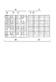
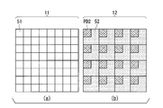
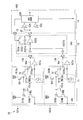
- FIG. 4 is a diagram schematically illustrating an example (first arrangement example) of the arrangement of the pixels 50 (the normal pixels 51 and the motion detection pixels 52) in the solid-state imaging device 1 according to the first embodiment of the present invention. .
- FIG. 4 shows an example of the arrangement of the normal pixels 51 and the motion detection pixels 52 in the pixel array unit 40 formed on each semiconductor substrate constituting the solid-state imaging device 1.
- the pixels 50 that is, the normal pixels 51 and the motion detection pixels 52 are arranged in a planar shape.
- the normal pixels 51 are formed on the first semiconductor substrate 11, and the motion detection pixels 52 are divided into the first semiconductor substrate 11 and the second semiconductor substrate 12.
- Form. 4A shows an example in which the pixels 50 (the normal pixels 51 and the motion detection pixels 52) are arranged in the region of the pixel array unit 40 of the first semiconductor substrate 11 constituting the solid-state imaging device 1.
- FIG. 4B shows an example in which the motion detection pixels 52 are arranged in the region of the pixel array section 40 of the second semiconductor substrate 12 constituting the solid-state imaging device 1.
- the output circuit is periodically arranged in the row direction and the column direction.
- the normal pixels 51 are arranged more than the motion detection pixels 52 as shown in FIG.
- the photoelectric conversion elements PD2 and output circuits of the normal pixels 51 and the motion detection pixels 52 are alternately arranged.
- the photoelectric conversion element PD ⁇ b> 2 of the motion detection pixel 52 disposed on the first semiconductor substrate 11 is located in a planar region of the pixel array unit 40 of the second semiconductor substrate 12.
- a readout circuit for the motion detection pixel 52 corresponding to the output circuit is arranged.
- the readout circuit of the motion detection pixel 52 is a pixel array unit 40 of the second semiconductor substrate 12 corresponding to the normal pixel 51 arranged on the first semiconductor substrate 11. It is formed including the planar area. That is, in the solid-state imaging device 1, the motion detection pixel 52 that requires a large area when forming because it is composed of more circuit elements than the normal pixel 51 is used to form the normal pixel 51.
- the region of the second semiconductor substrate 12 that is not present. More specifically, in the second semiconductor substrate 12 stacked on the surface opposite to the surface on which light is incident on the normal pixel 51, the region of the normal pixel 51 formed on the first semiconductor substrate 11 A readout circuit for the motion detection pixel 52 is formed including the overlapping region. Then, as shown in FIGS. 4A and 4B, the output circuit formed on the first semiconductor substrate 11 and the read circuit formed on the second semiconductor substrate 12 are connected to each other in a chip connection. Electrical connection is made by the section 13.
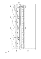
- FIG. 5 is a cross-sectional view showing an example of the structure of the solid-state imaging device 1 according to the first embodiment of the present invention.
- FIG. 5 shows a partial vertical structure of the pixel array unit 40 in the case where the normal pixels 51 and the motion detection pixels 52 are arranged as in the first arrangement example in the solid-state imaging device 1. More specifically, there are three normal pixels 51 formed on the first semiconductor substrate 11 and one motion detection pixel 52 formed on the first semiconductor substrate 11 and the second semiconductor substrate 12. The vertical structure is shown.
- FIG. 5 shows a state in which a switched capacitor amplifier circuit 523 and an AER circuit 526 provided in the readout circuit of the motion detection pixel 52 formed in the second semiconductor substrate 12 are formed.
- the output circuit of the motion detection pixel 52 and the readout circuit of the corresponding motion detection pixel 52 are provided between the first semiconductor substrate 11 and the second semiconductor substrate 12. Electrical connection is made by the chip connecting portion 13 formed in the step.
- the solid-state imaging in which a color filter (color filter) CF is pasted on the side where light is incident on each of the normal pixel 51 and the motion detection pixel 52.
- the structure of the apparatus 1 is shown. That is, the configuration of the solid-state imaging device 1 that outputs a pixel signal for generating a color image in normal photographing is shown.
- the color filter CF to be pasted at the position where the normal pixel 51 is disposed is, for example, each color similar to the color filter of the Bayer array, that is, the wavelengths of red (R), green (G), and blue (B). It is a color filter corresponding to light in a band.
- the color filter CF attached to the position where the motion detection pixel 52 is disposed is preferably a color filter corresponding to light in a white (W) wavelength band, for example.
- the motion detection pixel 52 can detect the motion of the subject, not by light of a specific wavelength band.
- the color and arrangement of the color filter CF attached to the solid-state imaging device 1 are not particularly defined.
- the color filter CF that is attached to the position where the motion detection pixel 52 is disposed is a color filter CF that transmits light in the near-infrared wavelength band, so that the motion detection pixel 52 has a wavelength of near-infrared.
- the movement of the subject may be detected by the light in the band.
- the method of allowing light in the near-infrared wavelength band to enter the motion detection pixel 52 is not limited to the method using the characteristics of the color filter CF, and for example, at the position of the motion detection pixel 52. Only a method in which an infrared cut filter that removes light in the near-infrared wavelength band is not disposed may be used.
- the pixel array unit includes the normal pixel 51 specialized for the output of the pixel signal by the normal photographing and the motion detection pixel 52 specialized for the output of the event pixel signal by the motion detection.
- the solid-state imaging device 1 sequentially reads out pixel signals in normal shooting by the normal pixels 51 in units of frames by normal reading.
- event pixels are sequentially detected at a timing that is not related to normal readout in which pixel signals are read out in units of frames in normal imaging by motion detection readout. Output a signal. Therefore, the solid-state imaging device 1 can perform normal readout and motion detection readout simultaneously.
- the number of normal pixels 51 arranged in the pixel array unit 40 is larger than that of the motion detection pixels 52 as in the first arrangement example described above.
- the motion detection pixels 52 arranged in the pixel array unit 40 are divided into the first semiconductor substrate 11 and the second semiconductor substrate 12, thereby forming the inside of the pixel array unit 40. It is possible to increase the number of normal pixels 51 arranged in the. Thereby, in the solid-state imaging device 1, it is possible to suppress a decrease in image quality of an image generated in normal shooting.
- the image processing unit that generates an image based on the pixel signal in normal photographing output from the solid-state imaging device 1 generates a motion detection pixel in the solid-state imaging device 1 when generating an image based on each pixel signal.
- An image including the pixel signals of all the pixels is generated by interpolating the pixel signal of the position where 52 is arranged, that is, the pixel signal of the missing pixel.
- the image processing unit when an image is generated from the pixel signal read out from the normal pixel 51 by normal reading, the pixel signal of the normal pixel 51 corresponding to the position where the motion detection pixel 52 is arranged is used as the peripheral normal pixel 51. Is interpolated based on the pixel signal.
- the image processing unit particularly defines a method (pixel interpolation calculation method) for interpolating the pixel signals of the respective normal pixels 51 corresponding to the positions where the motion detection pixels 52 are arranged. do not do.
- the motion detection pixels 52 arranged in the pixel array unit 40 are formed separately on the first semiconductor substrate 11 and the second semiconductor substrate 12.
- the photoelectric conversion element PD2 provided in the motion detection pixel 52 can be formed without reducing the area.
- the photoelectric conversion element PD2 provided in the motion detection pixel 52 can generate a larger charge signal corresponding to the motion of the subject. Thereby, in the solid-state imaging device 1, the fall of the precision of motion detection can be suppressed.
- the number of motion detection pixels 52 arranged in the pixel array unit 40 is smaller than the number of normal pixels 51.
- the detection of the movement of the subject does not require a higher resolution, that is, a higher image quality than an image generated in normal shooting.
- the photoelectric conversion element PD2 of the motion detection pixel 52 generates more charge signals even in a short time, and suppresses a decrease in the accuracy of motion detection. . That is, it is desirable that the speed of motion detection can be improved by increasing the area of the photoelectric conversion element PD2.
- the number of normal pixels 51 arranged in the pixel array unit 40 is further increased, thereby improving the image quality of an image generated in normal shooting, that is, high definition. It can also be configured to obtain an output.
- FIG. 6 is a diagram schematically illustrating another example (second arrangement example) of the arrangement of the pixels 50 (the normal pixel 51 and the motion detection pixel 52) in the solid-state imaging device 1 according to the first embodiment of the present invention. It is. 6, as in the first arrangement example of the normal pixels 51 and the motion detection pixels 52 illustrated in FIG. 4, the normal pixels in the pixel array unit 40 formed on the respective semiconductor substrates constituting the solid-state imaging device 1.
- 51 shows an example of the arrangement of 51 and motion detection pixels 52.
- the normal pixels 51 and the motion detection pixels 52 in the solid-state imaging device 1 illustrated in FIG. 6 as in the first arrangement example of the normal pixels 51 and the motion detection pixels 52 illustrated in FIG.
- the pixels 51 and the motion detection pixels 52 are arranged in a planar shape (periodically in the row direction and the column direction).
- the normal pixels 51 are changed in the same manner as the first arrangement example of the normal pixels 51 and the motion detection pixels 52 illustrated in FIG. 4.
- the motion detection pixels 52 are formed separately on the first semiconductor substrate 11 and the second semiconductor substrate 12.
- FIG. 6A shows an example in which high-definition normal pixels 51 and motion detection pixels 52 are arranged in the region of the pixel array unit 40 of the first semiconductor substrate 11 constituting the solid-state imaging device 1.
- FIG. 6B shows an example in which the motion detection pixels 52 are arranged in the region of the pixel array section 40 of the second semiconductor substrate 12 constituting the solid-state imaging device 1.
- the area required for arranging one normal pixel 51 is reduced, and the pixel array portion of the first semiconductor substrate 11 is reduced.
- a larger number of normal pixels 51 can be arranged in the area of 40 planes.
- the area required to arrange the motion detection pixels 52 is the same size as the motion detection pixels 52 in the arrangement of the normal pixels 51 and the motion detection pixels 52 shown in FIG. Accordingly, as shown in FIGS. 6A and 6B, the motion detection pixel 52 is formed using a region where more normal pixels 51 are arranged.
- the photoelectric conversion element PD2 and the output circuit of the motion detection pixel 52 are A planar region having the same size as that of the pixel 51 is used (see FIG. 4A), and the readout circuit for the motion detection pixel 52 is provided on the second semiconductor substrate 12 for four normal pixels 51. (See FIG. 4B).
- the pixel array unit 40 of the first semiconductor substrate 11 includes the pixel array unit 40.
- the photoelectric conversion element PD2 and the output circuit of the motion detection pixel 52 are formed using a plane area having a size corresponding to four of the normal pixels 51.
- motion detection is performed on the pixel array unit 40 of the second semiconductor substrate 12.
- a readout circuit for the pixel 52 is formed by using a planar area of the size of 16 normal pixels 51.
- the output circuit formed on the first semiconductor substrate 11 and the readout circuit formed on the second semiconductor substrate 12 Are electrically connected by the chip connecting portion 13 (see FIG. 6A and FIG. 6B).
- FIG. 7 is a cross-sectional view illustrating an example of another structure of the solid-state imaging device 1 according to the first embodiment of the present invention.
- the normal pixels 51 and the motion detection pixels 52 are arranged in the solid-state imaging device 1 as in the second arrangement example.
- the vertical structure of a part of the pixel array unit 40 in this case is shown. More specifically, there are six normal pixels 51 formed on the first semiconductor substrate 11 and one motion detection pixel 52 formed on the first semiconductor substrate 11 and the second semiconductor substrate 12. The vertical structure is shown.
- the high-definition normal pixels 51 are arranged on the first semiconductor substrate 11.
- the area of the photoelectric conversion element PD1 of the normal pixel 51 formed on the first semiconductor substrate 11 is smaller than the area of the photoelectric conversion element PD2 of the motion detection pixel 52.
- the readout circuit of the motion detection pixel 52 has a region that overlaps the region of the normal pixel 51 formed on the first semiconductor substrate 11. It forms in the area
- the switched capacitor amplifier circuit 523 provided in the readout circuit of the motion detection pixel 52 formed in the second semiconductor substrate 12 A state in which the AER circuit 526 is formed is shown.
- the output circuit of the motion detection pixel 52 and the corresponding readout circuit of the motion detection pixel 52 are illustrated in FIG. A state is shown in which electrical connection is made by a chip connection portion 13 formed between the substrate 11 and the second semiconductor substrate 12.
- the configuration of the solid-state imaging device 1 in which a microlens having the same size as the normal pixel 51 is formed on the light incident side of the motion detection pixel 52. Is shown. That is, the configuration of the solid-state imaging device 1 in which light enters from each of the two microlenses is shown in the photoelectric conversion element PD2 of the motion detection pixel 52.
- the shape of the microlens formed on the light incident side of the motion detection pixel 52 arranged in the solid-state imaging device 1 is not particularly defined.
- a microlens having a size different from the microlens corresponding to each of the normal pixels 51 that is, a microlens having a size corresponding to the motion detection pixel 52 is formed on the light incident side of the motion detection pixel 52. It may be configured to.
- the configuration of the solid-state imaging device 1 in which the color filter CF is pasted on the side where the light is incident on each of the normal pixel 51 and the motion detection pixel 52 is not particularly defined.
- the readout circuit of the motion detection pixel 52 is formed using a plane area having a size corresponding to four of the normal pixels 51, the motion detection pixel 52 is arranged.
- the color filter CF to be attached to the position is not only the color filter corresponding to the light of the white (W) wavelength band described above, but also red (R), two green (G), and blue (B) Each color filter corresponding to light in the wavelength band may be used.
- the color filter CF to be attached at the position where the motion detection pixel 52 is disposed is a color filter corresponding to light in the red (R), green (G), blue (B), and white (W) wavelength bands. May be.
- the color filter CF to be attached to the position where the motion detection pixel 52 is disposed is a color corresponding to light in the red (R), green (G), blue (B), and near infrared (Ir) wavelength bands. It may be a filter.
- each of the normal pixels 51 and the motion detection pixels 52 with high definition is arranged in the pixel array unit 40 to sequentially detect the movement of the subject.
- an image generated in normal shooting is increased in pixels to improve image quality.
- the first semiconductor substrate (first semiconductor substrate 11) on which light is incident and the first semiconductor substrate 11 are stacked on the surface opposite to the surface on which light is incident.
- the photoelectric conversion element (photoelectric conversion element PD1) and the first semiconductor substrate 11 are arranged corresponding to each of the n photoelectric conversion elements PD1, and the first photoelectric conversion element PD1 generated corresponding to the first photoelectric conversion element PD1 is generated.
- Reading circuit charge transfer transistor 511, pixel reset A driving circuit (vertical scanning circuit) that sequentially drives each of the read circuit of the n-number of normal pixels 51 by outputting the first pixel signal by sequentially driving the transistor 512, the amplification transistor 513, the selection transistor 514, and the node capacitance FD1). 20 and the horizontal scanning circuit 30), and m pieces of the second charge signal that are periodically arranged on one of the first semiconductor substrate 11 and the second semiconductor substrate 12 and photoelectrically convert incident light.
- Second photoelectric conversion element PD2 photoelectric conversion element PD2
- the second pixel representing a change in the second charge signal generated by one corresponding photoelectric conversion element PD2 among the m photoelectric conversion elements PD2.
- M number of second readout circuits that sequentially output signals (event pixel signals), and read the m motion detection pixels 52.
- Each circuit detects a temporal change in the second charge signal generated by the corresponding one photoelectric conversion element PD2, and indicates a changed direction when a change exceeding a predetermined threshold is detected.
- a detection circuit (threshold amplifier 524 and threshold amplifier 525) that outputs an event signal, and address information that is disposed on the second semiconductor substrate 12 and indicates a position where one photoelectric conversion element PD2 corresponding to the event signal is disposed.
- a solid-state image pickup device (solid-state image pickup device 1), wherein n is a natural number of 2 or more, and m is a natural number of 2 or more. ) Is configured.
- each of the readout circuits of the m motion detection pixels 52 is arranged on the second semiconductor substrate 12 and the second photoelectric conversion element PD2 generated by the corresponding one is generated. It further has an amplifier circuit (switched capacitor amplifier circuit 523) for amplifying the charge signal, and the threshold amplifier 524 and the threshold amplifier 525 detect a change in the second charge signal after being amplified by the switched capacitor amplifier circuit 523.
- the solid-state imaging device 1 is configured.
- m is smaller than n
- the area where each of the m photoelectric conversion elements PD2 receives light is the area where each of the n photoelectric conversion elements PD1 receives light.
- the solid-state imaging device 1 that is larger than that is configured.
- the circuit element of the first semiconductor substrate 11 and the circuit element of the second semiconductor substrate 12 are formed between the first semiconductor substrate 11 and the second semiconductor substrate 12.
- the connection unit 13 includes the solid-state imaging device 1 that electrically connects the threshold amplifier 524 and the threshold amplifier 525 included in each of the readout circuits of the m motion detection pixels 52 and the corresponding one photoelectric conversion element PD2. Composed.
- the normal pixel 51 specialized for outputting a pixel signal by normal photographing and the motion detection specialized for outputting an event pixel signal by motion detection.
- Each of the pixels 52 is periodically (planarly) arranged in the row direction and the column direction in the pixel array unit 40.
- the normal pixels 51 are formed on the first semiconductor substrate 11, and the motion detection pixels 52 are divided into the first semiconductor substrate 11 and the second semiconductor substrate 12.
- the photoelectric conversion element PD2 and the output circuit of the motion detection pixel 52 are formed on the first semiconductor substrate 11 and the readout circuit is formed on the first semiconductor substrate 11 in the second semiconductor substrate 12.
- the number of normal pixels 51 arranged in the pixel array unit 40 can be larger than that of the motion detection pixels 52, and an image generated in normal photographing can be generated. Image quality can be improved. Further, in the solid-state imaging device 1 of the first embodiment, the photoelectric conversion element PD2 of the motion detection pixel 52 arranged in the pixel array unit 40 can be enlarged, and a larger charge signal is generated according to the movement of the subject. Thus, it is possible to suppress a decrease in the accuracy of motion detection.
- each of the normal pixel 51 specialized for the output of the pixel signal by the normal photographing and the motion detection pixel 52 specialized for the output of the event pixel signal by the motion detection are provided. Therefore, it is possible to achieve both normal photographing and motion detection that sequentially detects the motion of the subject.
- the normal imaging pixel signal is read from the normal pixel 51 in units of frames by the normal readout and the motion detection pixel 52 at the asynchronous timing by the motion detection readout. It is possible to simultaneously read out pixel signals for motion detection.
- solid-state imaging device 2 in the second embodiment of the present invention are the same as those in the first embodiment shown in FIGS. 1 and 2.
- the general view and the general configuration are the same. Therefore, in the following description, in the constituent elements of the solid-state imaging device 2, the same reference numerals are used for the same constituent elements as the constituent elements of the solid-state imaging apparatus 1 of the first embodiment, and the respective constituent elements and operations are the same. The detailed description about is omitted.
- FIG. 8A shows an example of the configuration of the normal pixels 51 arranged in the pixel array unit 40 of the solid-state imaging device 2
- FIG. 8B shows the motion detection pixels 52 arranged in the pixel array unit 40 of the solid-state imaging device 2. An example of the configuration is shown.
- the configuration of the normal pixel 51 is the same as that of the normal pixel 51 in the solid-state imaging device 1 of the first embodiment illustrated in FIG. 3A as illustrated in FIG. 8A. Therefore, a detailed description of the configuration and operation of the normal pixel 51 is omitted.
- the configuration of the motion detection pixel 52 is the same as that of the motion detection pixel 52 in the solid-state imaging device 1 according to the first embodiment shown in FIG. 3B.
- the motion detection pixels 52 are formed on the second semiconductor substrate 12 as described above. That is, in the solid-state imaging device 2, the motion detection pixels 52 are not formed separately on the first semiconductor substrate 11 and the second semiconductor substrate 12 as in the solid-state imaging device 1 of the first embodiment.
- the second semiconductor substrate 12 is formed only. For this reason, the motion detection pixel 52 in the solid-state imaging device 2 does not include the chip connection unit 13.
- motion detection pixel 52 Other circuit elements included in the motion detection pixel 52 are the same as those of the motion detection pixel 52 in the solid-state imaging device 1 according to the first embodiment illustrated in FIG. 3B. Therefore, a detailed description of the configuration and operation of the motion detection pixel 52 is omitted.
- FIG. 9 is a diagram schematically illustrating an example (third arrangement example) of the arrangement of the pixels 50 (the normal pixels 51 and the motion detection pixels 52) in the solid-state imaging device 2 according to the second embodiment of the present invention. .
- FIG. 9 shows a pixel array section formed on each semiconductor substrate constituting the solid-state image pickup device 2 as in the first arrangement example of the pixels 50 in the solid-state image pickup device 1 of the first embodiment shown in FIG.
- An example of the arrangement of normal pixels 51 and motion detection pixels 52 within 40 is shown.
- the normal pixels 51 and the motion detection pixels 52 are arranged in a planar shape, similarly to the solid-state imaging device 1 of the first embodiment.
- the normal pixels 51 are formed on the first semiconductor substrate 11, and the motion detection pixels 52 are formed on the second semiconductor substrate 12. That is, in the solid-state imaging device 2, the motion detection pixels 52 are arranged so as to be stacked on the surface opposite to the surface on which light is incident on the normal pixels 51. In other words, in the solid-state imaging device 2, the motion detection pixel 52 is disposed on the back side of the normal pixel 51.
- light (light rays) transmitted through the normal pixel 51 is incident on the motion detection pixel 52.
- FIG. 9A shows an example in which normal pixels 51 are arranged in the region of the pixel array section 40 of the first semiconductor substrate 11 constituting the solid-state imaging device 2.
- FIG. 9B shows an example in which the motion detection pixels 52 are arranged in the region of the pixel array section 40 of the second semiconductor substrate 12 constituting the solid-state imaging device 2.
- the normal pixels 51 are arranged in the row direction and the column direction in the planar area of the pixel array section 40 of the first semiconductor substrate 11.
- the plane area of the pixel array unit 40 of the second semiconductor substrate 12 moves to the plane area of the pixel array unit 40 of the second semiconductor substrate 12.
- the detection pixels 52 are arranged in the row direction and the column direction.
- the photoelectric conversion element PD ⁇ b> 2 of the motion detection pixel 52 is placed in the first semiconductor substrate 11 in the planar area of the pixel array unit 40 of the second semiconductor substrate 12.
- the output circuit and the readout circuit of the motion detection pixel 52 are formed including the regions of the plurality of normal pixels 51 where the photoelectric conversion elements PD2 of the motion detection pixel 52 are not overlapped. That is, in the solid-state imaging device 2, a plurality of motion detection pixels 52 that require a larger area when formed because they are composed of more circuit elements than the normal pixels 51 are formed on the first semiconductor substrate 11. The region of the second semiconductor substrate 12 overlapping the region of the normal pixel 51 is formed.
- the second semiconductor substrate corresponding to the position where the photoelectric conversion element PD2 of the motion detection pixel 52 and the output circuit are arranged on the first semiconductor substrate 11.
- the photoelectric conversion elements PD2 of the motion detection pixels 52 are periodically arranged in a planar area of the twelve pixel array units 40. Note that, in the region where the photoelectric conversion element PD2 is disposed on the second semiconductor substrate 12, the output circuit of the motion detection pixel 52 may be included, as in the solid-state imaging device 1 of the first embodiment.
- each motion detection pixel 52 disposed on the second semiconductor substrate 12 transmits light that has passed through the region of the photoelectric conversion element PD1 of the normal pixel 51 disposed on the first semiconductor substrate 11.
- a charge signal obtained by photoelectrically converting (light) is generated.
- each motion detection pixel 52 arranged on the second semiconductor substrate 12 is detected by the motion detection arranged on the first semiconductor substrate 11 in the solid-state imaging device 1 of the first embodiment.
- An event pixel signal in which the movement of the subject is detected at the same position as the pixel 52 is output.
- the normal pixels 51 specialized for the output of the pixel signal by the normal photographing are arranged in the pixel array unit 40 of the first semiconductor substrate 11, and the event pixel signal is output by the motion detection.
- Motion detection pixels 52 specialized in the second semiconductor substrate 12 are arranged in the pixel array section 40 of the second semiconductor substrate 12 to detect the motion of the subject sequentially as in the solid-state imaging device 1 of the first embodiment.
- normal shooting Also in the solid-state imaging device 2, normal readout and motion detection readout can be performed simultaneously, as in the solid-state imaging device 1 of the first embodiment.
- the solid-state imaging device 2 can obtain the same effects as those of the solid-state imaging device 1 of the first embodiment. That is, even in the solid-state imaging device 2, it is possible to suppress a decrease in image quality of an image generated in normal shooting and to suppress a decrease in motion detection accuracy.
- the normal pixels 51 are arranged on the first semiconductor substrate 11 and the motion detection pixels 52 are arranged on the second semiconductor substrate 12 as in the third arrangement example described above.
- the image processing unit that generates an image based on the pixel signal in the normal shooting output from the solid-state imaging device 2 generates the pixel signal of the missing pixel when generating the image based on each pixel signal. There is no need to perform an operation to interpolate.
- FIG. 10 is a diagram schematically illustrating another example (fourth arrangement example) of the arrangement of the pixels 50 (the normal pixel 51 and the motion detection pixel 52) in the solid-state imaging device 2 according to the second embodiment of the present invention. It is. 10, as in the third arrangement example of the normal pixels 51 and the motion detection pixels 52 illustrated in FIG. 9, the normal pixels in the pixel array unit 40 formed on each semiconductor substrate constituting the solid-state imaging device 2. 51 shows an example of the arrangement of 51 and motion detection pixels 52.
- FIG. 10A shows an example in which high-definition normal pixels 51 are arranged in the row direction and the column direction in the region of the pixel array section 40 of the first semiconductor substrate 11 constituting the solid-state imaging device 2.
- FIG. 10B shows an example in which the motion detection pixels 52 are arranged in the row direction and the column direction in the region of the pixel array section 40 of the second semiconductor substrate 12 constituting the solid-state imaging device 2.
- the solid-state imaging device 2 By increasing the definition of the normal pixels 51, the solid-state imaging device 2 also has a smaller area required for arranging one normal pixel 51 as shown in FIG. A larger number of normal pixels 51 can be arranged in a planar region of the pixel array section 40 of the substrate 11.
- position the motion detection pixel 52 in the 2nd semiconductor substrate 12 is the same size as the area
- the area of the four normal pixels 51 formed on the first semiconductor substrate 11 is the same size.
- One motion detection pixel 52 is formed in the region of the second semiconductor substrate 12.
- the fourth arrangement example of the normal pixels 51 and the motion detection pixels 52 shown in FIG. 10 the same size as the area of 16 normal pixels 51 formed on the first semiconductor substrate 11 is used.
- One motion detection pixel 52 is formed in the region of the second semiconductor substrate 12.
- positioned at the 2nd semiconductor substrate 12 is 1st semiconductor.
- a charge signal is generated by photoelectrically converting light (light rays) transmitted through the region of the photoelectric conversion element PD1 of the four normal pixels 51 arranged on the substrate 11. Accordingly, in the solid-state imaging device 2 in which the normal pixels 51 and the motion detection pixels 52 are arranged as in the fourth arrangement example illustrated in FIG. 10, the respective motion detection pixels 52 arranged on the second semiconductor substrate 12.
- the fourth arrangement example in the solid-state imaging device 2 is arranged in the pixel array section 40 of the first semiconductor substrate 11 as in the second arrangement example in the solid-state imaging device 1 of the first embodiment.
- FIG. 11 is a cross-sectional view showing an example of the structure of the solid-state imaging device 2 according to the second embodiment of the present invention.
- FIG. 11 shows a partial vertical structure of the pixel array unit 40 in the case where the normal pixels 51 and the motion detection pixels 52 are arranged as in the third arrangement example in the solid-state imaging device 2. More specifically, four normal pixels 51 are formed on the first semiconductor substrate 11 and one motion detection pixel 52 is formed on the second semiconductor substrate 12. The vertical structure in the 3rd example of arrangement
- the normal pixel 51 is arranged on the first semiconductor substrate 11, and the second semiconductor overlapping the region of the normal pixel 51. It is formed in the region of the substrate 12. More specifically, the first semiconductor substrate 12 stacked on the surface opposite to the surface on which light is incident on the normal pixel 51 (the front side of the normal pixel 51) (the back side of the normal pixel 51) is connected to the first semiconductor substrate 12.
- the motion detection pixel 52 is formed including an area overlapping the area of the normal pixel 51 formed on the semiconductor substrate 11. In FIG.
- the photoelectric conversion element PD2 of the motion detection pixel 52 formed in the second semiconductor substrate 12 the photoelectric conversion element PD2 of the motion detection pixel 52 formed in the second semiconductor substrate 12, the switched capacitor amplifier circuit 523 and the AER circuit 526 provided in the readout circuit of the motion detection pixel 52 are formed. It shows the state. In the solid-state imaging device 2, the first semiconductor substrate 11 and the second semiconductor substrate 12 are not electrically connected, so that the chip connection portion 13 is not formed.
- the photoelectric conversion elements PD ⁇ b> 2 of the respective motion detection pixels 52 disposed on the second semiconductor substrate 12 are connected to the normal pixels 51 disposed on the first semiconductor substrate 11.
- a charge signal is generated by photoelectrically converting light (light rays) transmitted through the region of the photoelectric conversion element PD1.
- the photoelectric conversion element PD2 generates a larger charge signal as the light having a longer wavelength that transmits more through the first semiconductor substrate 11.
- the vertical structure of the solid-state imaging device 2 shown in FIG. 11 shows the configuration of the solid-state imaging device 2 in which the color filter CF is pasted on the side where light is incident on each of the normal pixels 51. That is, the configuration of the solid-state imaging device 2 that outputs a pixel signal for generating a color image in normal photographing is shown. Therefore, the photoelectric conversion element PD2 of the motion detection pixel 52 is transmitted through the color filter CF and the normal pixel 51 attached to the normal pixel 51 disposed on the first semiconductor substrate 11 stacked on the light incident side. Light enters.
- the color and arrangement of the color filter CF attached to the solid-state imaging device 2 are not particularly defined.
- the photoelectric conversion element PD2 formed on the second semiconductor substrate 12 generates a larger charge signal as the wavelength is longer.
- the photoelectric conversion element PD2 formed on the second semiconductor substrate 12 corresponds to, for example, light in the red (R) wavelength band that passes through the normal pixel 51 more because the wavelength is long. It is desirable to form it at a position corresponding to the normal pixel 51 to which the color filter CF is attached.
- an imaging system including the solid-state imaging device 2 includes a light source that emits infrared light and irradiates infrared light when detecting the motion of the subject to improve the accuracy of motion detection. It can also be.
- the solid-state imaging device 2 can detect the movement of the subject instead of using light in a specific wavelength band, as in the solid-state imaging device 1 of the first embodiment. For this reason, in FIG. 11, it is desirable that the light incident on the photoelectric conversion element PD ⁇ b> 2 formed on the second semiconductor substrate 12 through the first semiconductor substrate 11 is not light in a specific wavelength band.
- each of the normal pixels 51 arranged on the first semiconductor substrate 11 corresponds to light in the red (R), green (G), blue (B), and white (W) wavelength bands.
- the photoelectric conversion element PD2 formed on the second semiconductor substrate 12 is attached with the color filter CF corresponding to light in the white (W) wavelength band.
- the photoelectric conversion element PD2 formed on the second semiconductor substrate 12 may be formed at a position corresponding to the normal pixel 51 to which the color filter CF corresponding to light in the green (G) wavelength band is attached, for example. Good.
- the motion detection pixel 52 can detect the motion of the subject using light in the green (G) wavelength band that can be considered to represent luminance in an image generated by normal shooting.
- the color of the color filter CF attached to the normal pixel 51 is related. Disappear.
- the photoelectric conversion element PD ⁇ b> 2 of the motion detection pixel 52 includes a plurality of (four in FIG. 10B) planar areas having the size of the normal pixel 51. Is formed at a position including all the colors attached to the normal pixel 51, the color of the color filter CF attached to the normal pixel 51 becomes irrelevant.
- the vertical structure of the solid-state imaging device 2 shown in FIG. 11 shows the configuration of the solid-state imaging device 2 in which microlenses are formed on the side where light is incident on each of the normal pixels 51.
- FIG. 10B when the photoelectric conversion element PD2 of the motion detection pixel 52 is formed using a plane area having a size corresponding to four of the normal pixels 51, 4 Light incident from each of the two microlenses passes through the normal pixel 51 corresponding to each microlens, and enters the photoelectric conversion element PD2 of the motion detection pixel 52.
- light that has passed through the normal pixel 51 corresponding to light in the red (R), green (G), blue (B), and white (W) wavelength bands is applied to the photoelectric conversion element PD2 of the motion detection pixel 52.
- each of the m second photoelectric conversion elements (photoelectric conversion elements PD2) is arranged on the second semiconductor substrate (second semiconductor substrate 12), and the n first photoelectric conversion elements are arranged.
- the photoelectric conversion element photoelectric conversion element PD1
- a second charge signal obtained by photoelectrically converting light transmitted through the corresponding p photoelectric conversion elements PD1 is generated, and p is a natural number of 1 or more
- solid-state imaging A device solid-state imaging device 2 is configured.
- the normal pixel 51 specialized for the output of the pixel signal by normal photographing
- Each of the motion detection pixels 52 specialized for the output of the event pixel signal by motion detection is periodically (planarly) arranged in the row direction and the column direction in the pixel array unit 40.
- the normal pixels 51 are formed on the first semiconductor substrate 11 and the motion detection pixels 52 are formed on the second semiconductor substrate 12.
- the motion detection pixel 52 is a surface on the opposite side (the back side of the normal pixel 51) to the surface on which light is incident on the normal pixel 51 (the front side of the normal pixel 51).
- the number of normal pixels 51 arranged in the pixel array unit 40 is set to be larger than that of the motion detection pixels 52 as in the solid-state imaging device 1 of the first embodiment. The image quality of an image generated in normal shooting can be improved.
- the photoelectric conversion element PD2 of the motion detection pixel 52 arranged in the pixel array unit 40 may be increased. It is possible to generate a larger charge signal corresponding to the movement of the subject, and to suppress a decrease in the accuracy of the motion detection.
- the normal pixel 51 specialized for the output of the pixel signal by the normal photographing and the event pixel by the motion detection
- the motion detection pixels 52 specialized for signal output both normal photographing and motion detection for sequentially detecting the motion of the subject can be achieved.
- reading of a normal photographing pixel signal from the normal pixel 51 in units of frames by normal reading It is possible to simultaneously read out a pixel signal for motion detection from the motion detection pixel 52 at an asynchronous timing by the motion detection readout.
- solid-state imaging device 3 in the third embodiment of the present invention are the same as those in the first embodiment shown in FIGS. 1 and 2.
- the general view and the general configuration are the same. Therefore, in the following description, in the constituent elements of the solid-state imaging device 3, the same constituent elements as the constituent elements of the solid-state imaging apparatus 1 of the first embodiment are denoted by the same reference numerals, and the respective constituent elements and operations are the same. The detailed description about is omitted.
- the pixels 50 arranged in the pixel array unit 40 in the solid-state imaging device 3 of the third embodiment are also pixels for normal photographing by normal readout.
- a signal and an event pixel signal for motion detection by motion detection readout are output.
- the pixels 50 arranged in the pixel array unit 40 in the solid-state imaging device 3 obtain the normal imaging pixel signal and the event pixel signal from the charge signal generated by the same photoelectric conversion element.
- the photoelectric conversion element provided in the pixel 50 arranged in the pixel array unit 40 of the solid-state imaging device 3 is the pixel array unit 40 in the solid-state imaging device 1 of the first embodiment and the solid-state imaging device 2 of the second embodiment.
- the photoelectric conversion element PD1 provided in the normal pixel 51 disposed therein and the photoelectric conversion element PD2 provided in the motion detection pixel 52 are also used.
- the normal imaging pixel signal output by the normal readout and the motion detection event pixel signal output by the motion detection readout which are arranged in the pixel array unit 40 of the solid-state imaging device 3 are performed.
- the pixel 50 is referred to as a “shared pixel 53”.
- FIG. 12 is a circuit diagram illustrating an example (first configuration example) of the dual-purpose pixel 53 in the solid-state imaging device 3 according to the third embodiment of the present invention.
- the circuit elements constituting the dual-purpose pixel 53 include circuit elements constituting the normal pixel 51 or the motion detection pixel 52 arranged in the solid-state imaging device 1 of the first embodiment and the solid-state imaging device 2 of the second embodiment. Contains similar circuit elements. Therefore, in the following description, in the circuit elements constituting the dual-purpose pixel 53, the same reference numerals are given to the circuit elements similar to the circuit elements constituting the normal pixel 51 or the motion detection pixel 52, and detailed description thereof is omitted. To do.
- the dual-purpose pixel 53 includes a photoelectric conversion element PD12, a charge transfer transistor 511, a pixel reset transistor 512, an amplification transistor 513, a selection transistor 514, an amplifier 521, a bias transistor 522, and a switched capacitor amplifier circuit. 523, a threshold amplifier 524, a threshold amplifier 525, and an AER circuit 526.
- the switched capacitor amplifier circuit 523 includes a capacitor 5231, an amplifier 5232, a capacitor 5233, and a switch 5234.
- a node capacitance FD1 that is a capacitance associated with a node connected to the gate terminal of the amplification transistor 513 provided in the dual-purpose pixel 53 is indicated by a capacitor symbol as a circuit element of the dual-purpose pixel 53.
- a charge signal generated by normal imaging is generated by the configuration of the photoelectric conversion element PD12, the charge transfer transistor 511, the pixel reset transistor 512, the amplification transistor 513, the selection transistor 514, and the node capacitor FD1.
- a pixel that is, a pixel similar to the normal pixel 51 in the solid-state imaging device 1 of the first embodiment and the solid-state imaging device 2 of the second embodiment is configured.
- the dual-purpose pixel 53 that generates a charge signal by normal photographing is referred to as a “normal-purpose pixel 531”.
- the charge transfer transistor 511, the pixel reset transistor 512, the amplification transistor 513, the selection transistor 514, and the node capacitor FD1 correspond to the charge signal generated by the photoelectric conversion element PD12 in normal photographing.
- a readout circuit for reading out pixel signals is configured.
- the photoelectric conversion element PD12, the amplifier 521, the bias transistor 522, the switched capacitor amplifier circuit 523, the threshold amplifier 524, the threshold amplifier 525, and the AER circuit 526 are used for motion detection. That is, a pixel similar to the motion detection pixel 52 in the solid-state imaging device 1 of the first embodiment and the solid-state imaging device 2 of the second embodiment is configured.
- the combined pixel 53 that generates a charge signal for motion detection is referred to as a “motion detection combined pixel 532”.
- the amplifier 521 and the bias transistor 522 constitute an output circuit that outputs a charge signal generated by the photoelectric conversion element PD12 for motion detection, and includes a switched capacitor amplifier circuit 523, a threshold amplifier 524, The threshold amplifier 525 and the AER circuit 526 form a readout circuit that reads out a charge signal generated by the photoelectric conversion element PD12 for motion detection.
- the dual-purpose pixels 53 are uniformly arranged over the entire planar area of the pixel array unit 40.
- the photoelectric conversion element PD 12 the readout circuit for the normal / shared pixel 531, and the output circuit for the motion detection / shared pixel 532 are formed on the first semiconductor substrate 11.
- a readout circuit for the motion detection / use pixel 532 is formed on the second semiconductor substrate 12.
- the photoelectric conversion element PD12 is the same as the photoelectric conversion element PD1 provided in the normal pixel 51 and the photoelectric conversion element provided in the motion detection pixel 52 in the solid-state imaging device 1 of the first embodiment and the solid-state imaging device 2 of the second embodiment. Similar to PD2, it is a photodiode that photoelectrically converts incident light (light beam) to generate a charge signal and accumulates the generated charge signal. The photoelectric conversion element PD12 sequentially outputs the generated charge signal to the amplifier 521.
- the amplifier 521 controls bias.
- a voltage signal Vp that causes the bias transistor 522 to be always ON is output to the gate terminal of the bias transistor 522. That is, when a pixel signal obtained by normal photographing is output from the dual-purpose pixel 53, the charge signal generated by the photoelectric conversion element PD 12 is transmitted to the charge transfer transistor 511 as it is by the bias transistor 522.
- the charge transfer transistor 511 generates and accumulates the photoelectric conversion element PD12 in accordance with the control signal TX input from the vertical scanning circuit 20, and the charge signal input via the bias transistor 522 is amplified. Transfer to the gate terminal of 513. As a result, the charge signal transferred by the charge transfer transistor 511 is accumulated in the node capacitor FD1.
- the dual-purpose pixel 53 (normal dual-purpose pixel 531) reads out each signal voltage corresponding to the charge signal obtained by photoelectric conversion of the light incident on the photoelectric conversion element PD12 to the vertical signal line 60 as a pixel signal.
- the vertical scanning circuit 20 controls the control signal RST so that the pixel reset transistor 512 is always ON. Further, the vertical scanning circuit 20 controls the control signal TX to a fixed bias voltage. Accordingly, a fixed voltage corresponding to a fixed bias voltage is supplied to the bias transistor 522 by the pixel reset transistor 512 and the charge transfer transistor 511.
- the photoelectric conversion element PD12 generates a charge signal having a magnitude corresponding to the movement of the subject, and changes the charge signal in the change direction. A corresponding event pixel signal is output.
- the normal dual-purpose pixel 531 and the motion detection dual-purpose pixel 532 also serve as the photoelectric conversion element PD12. For this reason, in the solid-state imaging device 3, the readout of the normal photographing pixel signal from the normal / use pixel 531 in the frame unit by the normal readout and the motion detection from the motion detection / use pixel 532 at the asynchronous timing by the motion detection readout. The pixel signal is read out exclusively.
- FIG. 13 is a timing chart showing an example of timing for driving the dual-purpose pixel 53 in the solid-state imaging device 3 according to the third embodiment of the present invention.
- the timing chart shown in FIG. 13 controls the dual-purpose pixel 53 of the first configuration example so as to perform exposure for motion detection after outputting a pixel signal obtained by normal photographing to the vertical signal line 60.
- the control timing of the vertical scanning circuit 20 is shown.
- all the shared pixels 53 in the pixel array section 40 are reset at time t1. More specifically, at time t1, the vertical scanning circuit 20 simultaneously sets the control signal RST and the control signal TX to “High” level, and turns on the pixel reset transistor 512 and the charge transfer transistor 511. As a result, the photoelectric conversion elements PD12 and the node capacitance FD1 provided in all the shared pixels 53 in the pixel array section 40 are reset.
- the vertical scanning circuit 20 sets the control signal RST and the control signal TX to the “Low” level at the same time, turns off the pixel reset transistor 512 and the charge transfer transistor 511, and uses all of the common functions in the pixel array unit 40.
- the reset of the pixel 53 is cancelled.
- all the shared pixels 53 in the pixel array unit 40 start exposure simultaneously. That is, the photoelectric conversion elements PD12 provided in all the dual-purpose pixels 53 in the pixel array unit 40 start generating and accumulating charge signals obtained by photoelectrically converting incident light.
- pixel signals from the dual-purpose pixels 53 in the pixel array unit 40 are normally read from time t2. .
- the vertical scanning circuit 20 sets the control signal SEL to “High” level, turns on the selection transistor 514, and connects the amplification transistor 513 to the vertical signal line 60. Put it in a state. As a result, the signal voltage output from the amplification transistor 513 is output to the vertical signal line 60 via the selection transistor 514.
- the vertical scanning circuit 20 sets the control signal RST to the “High” level, turns on the pixel reset transistor 512, and resets the node capacitor FD1.
- the signal voltage at the reset level of the photoelectric conversion element PD12 is output from the amplification transistor 513 to the vertical signal line 60 by the selection transistor 514.
- the vertical scanning circuit 20 sets the control signal RST to the “Low” level, turns off the pixel reset transistor 512, and releases the reset of the node capacitor FD1.
- the vertical scanning circuit 20 sets the control signal TX to “High” level to turn on the charge transfer transistor 511, and the charge signal accumulated in the photoelectric conversion element PD12 is transferred to the gate of the amplification transistor 513. Transfer to the terminal. At this time, the charge signal transferred by the charge transfer transistor 511 is accumulated in the node capacitor FD1. Thereby, a charge signal generated by the photoelectric conversion element PD12 from the amplification transistor 513, that is, a signal voltage corresponding to the charge signal accumulated in the node capacitor FD1 is output to the vertical signal line 60 via the selection transistor 514.
- the difference between the reset level signal voltage output at time t3 and the signal voltage corresponding to the charge signal generated by the photoelectric conversion element PD12 output at time t4 is obtained. Then, noise removal processing may be performed on the pixel signal.
- the vertical scanning circuit 20 sets the control signal TX to “Low” level, turns off the charge transfer transistor 511, and stops the transfer of the charge signal accumulated in the photoelectric conversion element PD12 to the gate terminal of the amplification transistor 513.
- the control signal SEL is set to the “Low” level, the selection transistor 514 is turned off, and the amplification transistor 513 is disconnected from the vertical signal line 60.
- pixel signals corresponding to the charge signals generated by the photoelectric conversion elements PD12 provided in all the dual-purpose pixels 53 in the pixel array section 40 are read out by normal reading.
- FIG. 13 shows the control timing of the vertical scanning circuit 20 for one dual-purpose pixel 53.
- all the vertical scanning circuits 20 are arranged in the pixel array unit 40 of the solid-state imaging device 3.
- the normal photographing pixel signal is read from the dual-purpose pixel 53 in units of frames.
- the vertical scanning circuit 20 sequentially performs the normal reading control from time t2 to time t5 for each row of the dual-purpose pixels 53 arranged in the pixel array section 40, whereby the pixels in the respective rows.
- the signals are sequentially output to the vertical signal line 60.
- the horizontal scanning circuit 30 sequentially outputs the pixel signals of the respective rows output to the vertical signal lines 60 of the respective columns for each column, thereby converting all the pixel signals of one frame into the solid-state imaging device 3. To the outside.
- motion detection by each dual-purpose pixel 53 in the pixel array unit 40 that is, motion detection reading can be performed from time t6. Become.
- the vertical scanning circuit 20 sets the control signal RST to “High” level and turns on the pixel reset transistor 512.
- the vertical scanning circuit 20 sets the control signal TX to a fixed bias voltage.
- a fixed voltage corresponding to a fixed bias voltage is supplied from the charge transfer transistor 511 to the bias transistor 522.
- the dual-purpose pixel 53 sequentially outputs an event pixel signal based on a pulse signal corresponding to the charge signal generated by the photoelectric conversion element PD12.
- the vertical scanning circuit 20 controls the normal readout from the time t1 to the time t5 described above after first setting the state before the time t1. I do. More specifically, the vertical scanning circuit 20 sets each of the control signal RST and the control signal TX to the “Low” level and temporarily turns off the pixel reset transistor 512 and the charge transfer transistor 511, and then Each control described in t1 to time t5 is performed.
- each of the dual-purpose pixels 53 arranged in the pixel array unit 40 of the solid-state imaging device 3 is asynchronous with the readout of the normal imaging pixel signal in frame units by the normal readout and the motion detection readout.
- the pixel signal for motion detection at the timing is exclusively read out.
- the dual-purpose pixels 53 that perform the output of the pixel signal by the normal photographing and the output of the event pixel signal by the motion detection are uniformly arranged in the pixel array unit 40, thereby Similar to the solid-state imaging device 1 of the embodiment and the solid-state imaging device 2 of the second embodiment, it is possible to achieve both the motion detection for sequentially detecting the motion of the subject and the normal photographing.
- the dual-purpose pixels 53 are arranged uniformly over the entire planar area of the pixel array unit 40. For this reason, in the solid-state imaging device 3, the output circuit and the readout circuit of the motion detection / combining pixel 532 configured in the dual-purpose pixel 53 are separately formed on the first semiconductor substrate 11 and the second semiconductor substrate 12.
- the normal-purpose pixel 531 configured in the dual-purpose pixel 53 can be refined, that is, the number of normal-purpose pixels 531 arranged in the pixel array unit 40 can be increased.
- the area required for forming the readout circuit of the detection / use pixel 532 is within a range where a necessary area can be secured.
- the image quality of an image generated in normal shooting is improved by arranging more normal use pixels 531 and the motion detection use pixel 532 has a larger charge signal. It is desirable to suppress a decrease in accuracy of motion detection by detecting the motion of the subject based on the above.
- the solid-state imaging device 3 as well, based on the same idea (see FIGS. 4 to 7) as the first arrangement example and the second arrangement example of the pixels 50 in the solid-state imaging device 1 of the first embodiment. It is also conceivable to arrange the shared pixels 53. More specifically, in the solid-state imaging device 1 according to the first embodiment, it is conceivable to arrange the combined pixels 53 instead of the motion detection pixels 52 arranged in the pixel array unit 40. However, in the solid-state imaging device 3, the configuration of the dual-purpose pixel 53 can be changed to improve the image quality of an image generated in normal shooting, that is, to achieve a high pixel count and the accuracy of motion detection. Can be suppressed.
- the pixel 50 of the second configuration example improves the image quality of an image generated in normal shooting by increasing the definition of the normal dual-purpose pixel 531 that generates a charge signal by normal shooting.
- it is a pixel configured to suppress a decrease in accuracy of motion detection by increasing the number of photoelectric conversion elements PD12 shared by the motion detection / use pixel 532 that generates a charge signal for motion detection.
- FIG. 14 is a circuit diagram showing another example (second configuration example) of the pixel 50 in the solid-state imaging device 3 according to the third embodiment of the present invention.
- FIG. 14 shows a dual-purpose pixel 54 that includes two high-definition normal-purpose pixels 531 and one motion detection-purpose pixel 542.
- the circuit elements constituting the dual-purpose pixel 54 include circuit elements similar to the circuit elements constituting the dual-purpose pixel 53 of the first configuration example. Therefore, in the following description, in the circuit elements constituting the dual-purpose pixel 54, the same circuit elements as the circuit elements constituting the dual-purpose pixel 53 of the first configuration example are given the same reference numerals, and the detailed description will be given. Omitted.
- Each of the two normal dual-purpose pixels 531 provided in the dual-purpose pixel 54 has the same configuration as the normal dual-purpose pixel 531 configured in the dual-purpose pixel 53 of the first configuration example.
- each of the two normal-purpose pixels 531 is distinguished as a normal-use pixel 531a and a normal-use pixel 531b.
- a code given to distinguish each of the normal-use pixels 531 following the reference numerals of the respective circuit elements that is, “a "Or" b ".
- the normal-purpose pixel 531a includes a photoelectric conversion element PD12a, a charge transfer transistor 511a, a pixel reset transistor 512a, an amplification transistor 513a, a selection transistor 514a, and a node capacitor FD1a.
- the normal-purpose pixel 531b includes a photoelectric conversion element PD12b, a charge transfer transistor 511b, a pixel reset transistor 512b, an amplification transistor 513b, a selection transistor 514b, and a node capacitor FD1b.
- the operations of the normal / normal pixel 531a and the normal / common pixel 531b and the control timing by the vertical scanning circuit 20 are the same as those of the normal / common pixel 531 configured in the dual-purpose pixel 53 of the first configuration example. Description is omitted.
- the single motion detection / combining pixel 542 included in the dual-purpose pixel 54 has the same configuration as the motion detection / combining pixel 532 configured in the dual-purpose pixel 53 of the first configuration example.
- one motion detection / use pixel 542 serves as a plurality of normal / use pixels 531 and the photoelectric conversion element PD12.
- one motion detection / use pixel 542 serves as both the high-definition normal / common pixel 531 a and normal / use pixel 531 b and the photoelectric conversion element PD 12. That is, the motion detection / use pixel 542 detects the movement of the subject based on the charge signals generated by the plurality of photoelectric conversion elements PD12. For this reason, in the motion detection / use pixel 542, the configuration of circuit elements corresponding to the respective photoelectric conversion elements PD12 is changed.
- each of the motion detection combined pixel 542 includes an amplifier 521 provided in the motion detection combined pixel 532 in the first configuration example, a bias transistor 522, and a capacitor 5231 provided in the switched capacitor amplifier circuit 523.
- the configuration corresponds to each photoelectric conversion element PD12.
- the circuit element corresponding to any one photoelectric conversion element PD12 in the circuit element in the motion detection / use pixel 542 has a sign (“a” or “b” given to the photoelectric conversion element PD12. ”) Following the reference numerals of the respective circuit elements, the photoelectric conversion elements PD12 corresponding to the respective circuit elements are distinguished.
- the motion detection combined pixel 542 includes an amplifier 521a and an amplifier 521b, a bias transistor 522a and a bias transistor 522b, a switched capacitor amplifier circuit 543, a threshold amplifier 524 and a threshold amplifier 525, and an AER circuit 526. It is configured.
- the switched capacitor amplifier circuit 543 includes capacitors 5231a and 5231b, an amplifier 5232, a capacitor 5233, and a switch 5234.
- the amplifier 521a amplifies the charge signal generated and output by the corresponding photoelectric conversion element PD12a, and outputs the amplified charge signal to the capacitor 5231a in the switched capacitor amplifier circuit 543 via the chip connection unit 13a.
- the amplifier 521a transfers the amplified charge signal as a voltage signal Vpa to the gate terminal of the bias transistor 522a.
- the amplifier 521b amplifies the charge signal generated and output by the corresponding photoelectric conversion element PD12b, and outputs the amplified charge signal to the capacitor 5231b in the switched capacitor amplifier circuit 543 via the chip connection unit 13b.
- the amplifier 521b transfers the amplified charge signal as a voltage signal Vpb to the gate terminal of the bias transistor 522b.
- the bias transistor 522a has a constant current flowing through the photoelectric conversion element PD12a in accordance with the voltage signal Vpa transferred to the gate terminal, that is, even when the charge signal generated by the photoelectric conversion element PD12a changes. Control is performed so that the charge signal is successively stabilized at the magnitude after the magnitude of the charge signal is changed. That is, the output of the photoelectric conversion element PD12a is clipped.
- the bias transistor 522b allows the current flowing through the photoelectric conversion element PD12b to be a constant current according to the voltage signal Vpb transferred to the gate terminal, that is, even when the charge signal generated by the photoelectric conversion element PD12b changes. Control is performed so that the charge signal is successively stabilized at the magnitude after the magnitude of the charge signal is changed. That is, the output of the photoelectric conversion element PD12b is clipped.
- the switched capacitor amplifier circuit 543 adds the charge signals input from the amplifier 521a and the amplifier 521b via the corresponding chip connection part 13a or chip connection part 13b. More specifically, the capacitor 5231a accumulates the charge signal input from the corresponding amplifier 521a to the first terminal, and outputs a voltage signal having a voltage corresponding to the accumulated charge signal from the second terminal. The capacitor 5231b accumulates the charge signal input to the first terminal from the corresponding amplifier 521b, and outputs a voltage signal having a voltage corresponding to the accumulated charge signal from the second terminal. At this time, since the second terminal of the capacitor 5231a and the second terminal of the capacitor 5231b are connected as shown in FIG.
- the switched capacitor amplifier circuit 543 is similar to the switched capacitor amplifier circuit 523 provided in the dual-purpose pixel 53 of the first configuration example, and changes in the added charge signal, that is, each of the photoelectric conversion element PD12a and the photoelectric conversion element PD12b.
- the increase / decrease in the charge signal obtained by adding the charge signal generated by the signal is converted into a voltage signal in a predetermined voltage range and output to each of the threshold amplifier 524 and the threshold amplifier 525.
- the operation of the motion detection / use pixel 542 and the control timing by the vertical scanning circuit 20 are the same as those in the dual purpose pixel 53 of the first configuration example, except that the motion detection / use pixel 542 operates based on the added charge signal. Since this is the same as the motion detection / use pixel 532, detailed description is omitted.
- the dual-purpose pixel 54 improves the image quality of an image generated in normal shooting by the high-definition normal-purpose pixel 531 and increases the number of photoelectric conversion elements PD12 shared by the motion detection-purpose pixel 542. By doing so, it is possible to suppress a decrease in the accuracy of motion detection.
- the dual-purpose pixels 54 are arranged uniformly over the entire planar area of the pixel array unit 40.
- the output circuit of the motion detection / combination pixel 542 is formed on the first semiconductor substrate 11, and the readout circuit of the motion detection / combination pixel 542 is formed on the second semiconductor substrate 12.
- FIG. 15 is a sectional view showing an example of another structure of the solid-state imaging device 3 according to the third embodiment of the present invention.
- FIG. 15 shows a partial vertical structure of the pixel array unit 40 in the case where the dual-purpose pixels 54 of the second configuration example are arranged in the solid-state imaging device 3. More specifically, a vertical structure of a part of the pixel array unit 40 in which two dual-purpose pixels 54 are arranged is shown. More specifically, four normal-use pixels 531 formed on the first semiconductor substrate 11 and two motion detection-use pixels 542 formed on the first semiconductor substrate 11 and the second semiconductor substrate 12. The vertical structure is shown.
- each photoelectric conversion element PD 12, the readout circuit for the normal / capable pixel 531, and the output circuit for the motion detection / compatibility pixel 542 are formed on the first semiconductor substrate 11.
- a readout circuit for the detection / combination pixel 542 is formed on the second semiconductor substrate 12.
- FIG. 15 shows a state in which the switched capacitor amplifier circuit 543 and the AER circuit 526 provided in the readout circuit of the motion detection / use pixel 542 formed in the second semiconductor substrate 12 are formed.
- the output circuit corresponding to each photoelectric conversion element PD 12 shared by the motion detection / use pixel 542 and the switched capacitor amplifier circuit 543 provided in the readout circuit of the motion detection / use pixel 542. are electrically connected by respective chip connection portions 13 formed between the first semiconductor substrate 11 and the second semiconductor substrate 12.
- FIG. 15 shows an output circuit corresponding to the photoelectric conversion element PD12a provided in the normal-purpose pixel 531a formed on the first semiconductor substrate 11, and a capacitor 5231a in the switched capacitor amplifier circuit 543 formed on the second semiconductor substrate 12. Are shown as being connected by the chip connecting portion 13a. Further, FIG.
- FIG. 15 shows an output circuit corresponding to the photoelectric conversion element PD12b provided in the normal-purpose pixel 531b formed on the first semiconductor substrate 11, and a switched capacitor amplifier circuit 543 formed on the second semiconductor substrate 12. A state in which the capacitor 5231b is connected by the chip connecting portion 13b is shown.
- the configuration of the solid-state imaging device 3 in which the color filter CF is pasted on the side where the light enters each dual-purpose pixel 54 is shown.
- the color and arrangement of the color filter CF attached to the solid-state imaging device 1 are not particularly defined. That is, in the solid-state imaging device 3, the color filter CF is the same as the solid-state imaging device 1 of the first embodiment and the solid-state imaging device 2 of the second embodiment.
- the movement for sequentially detecting the movement of the subject is performed as in the solid-state imaging device 3 in which the dual-purpose pixel 53 in the first configuration example is arranged. It is possible to achieve both detection and normal shooting. Furthermore, in the solid-state imaging device 3 in which the dual-purpose pixel 54 of the second configuration example is arranged, the image quality of an image generated in normal shooting is improved by the high-definition normal-purpose pixel 531 and a plurality of motion detection / shared pixels 542 are provided. By also using the photoelectric conversion element PD12, it is possible to suppress a decrease in the accuracy of motion detection.
- one motion detection / shared pixel 542 includes two normal-use pixels 531 (the normal-purpose pixel 531a and the normal-purpose pixel 531b) and the photoelectrical pixel.
- a configuration in which the conversion element PD12 (the photoelectric conversion element PD12a and the photoelectric conversion element PD12b) is also used is shown.
- the configuration of the dual-purpose pixel 54 in the second configuration example is not limited to the configuration shown in FIG. In other words, the number of photoelectric conversion elements PD12 shared by one motion detection / shared pixel 542 in the dual-purpose pixel 54 of the second configuration example is not limited to the two shown in FIG.
- one motion detection / shared pixel 542 is configured to share the four normal / shared pixels 531 and the photoelectric conversion element PD12, that is, four motion detection / shared pixels 542.
- the movement of the subject may be detected based on the charge signal obtained by adding the charge signals generated by the photoelectric conversion element PD12.
- each photoelectric conversion element PD12 is a circuit element that constitutes the high-definition normal-purpose pixel 531.
- the area of each photoelectric conversion element PD12 may be further reduced as the normal-purpose pixel 531 has a higher definition.
- the solid-state imaging device 3 can be configured to reduce the number of chip connection portions 13 by changing the method of forming circuit elements of the dual-purpose pixels 54 formed on each semiconductor substrate.
- the pixel 50 of the third configuration example (hereinafter referred to as “combined pixel 55”) is necessary for the dual-purpose pixel 54 of the second configuration example in which the normal-use pixel 531 that generates a charge signal by normal photographing is increased in definition.
- This is a pixel having a configuration in which the number of chip connection portions 13 is reduced.
- the dual-purpose pixel 55 is a pixel having a configuration that improves the image quality of an image generated in normal shooting and suppresses the decrease in the accuracy of motion detection, similarly to the dual-purpose pixel 54 of the second configuration example.
- FIG. 16 is a circuit diagram showing still another example (third configuration example) of the configuration of the pixel 50 in the solid-state imaging device 3 according to the third embodiment of the present invention.
- the circuit elements constituting the dual-purpose pixel 55 include circuit elements similar to the circuit elements constituting the dual-purpose pixel 54 of the second configuration example. Therefore, in the following description, in the circuit elements constituting the dual-purpose pixel 55, the same circuit elements as the circuit elements constituting the dual-purpose pixel 54 of the second configuration example are given the same reference numerals, and the detailed description will be given. Omitted.
- Each of the two normal dual-purpose pixels 531 provided in the dual-purpose pixel 55 is the same as the normal dual-purpose pixel 531 configured in the dual-purpose pixel 54 of the second configuration example. Therefore, the detailed description regarding the normal-purpose pixel 531 is omitted.
- one motion detection / combining pixel 552 provided in the dual-purpose pixel 55 has the same configuration as the motion detection / combining pixel 542 configured in the dual-purpose pixel 54 of the second configuration example. Accordingly, the reference numerals assigned to the motion detection / combining pixel 552 in FIG. 16 are the same as those of the dual-purpose pixel 54 of the second configuration example. However, in the motion detection / combination pixel 552, in order to reduce the number of chip connection portions 13, the configuration of the circuit elements provided in the motion detection / combination pixel 542 configured in the dual-purpose pixel 54 of the second configuration example is changed. Yes.
- the motion detection combined pixel 552 includes an amplifier 521a and an amplifier 521b, a bias transistor 522a and a bias transistor 522b, a switched capacitor amplifier circuit 553, a threshold amplifier 524 and a threshold amplifier 525, and an AER circuit 526. It is configured.
- the switched capacitor amplifier circuit 553 includes capacitors 5231a and 5231b, an amplifier 5232, a capacitor 5233, and a switch 5234.
- the switched capacitor amplifier circuit 543 provided in the motion detection shared pixel 542 configured in the shared pixel 54 of the second configuration example is changed to a switched capacitor amplifier circuit 553.
- the switched capacitor amplifier circuit 553 is similar to the switched capacitor amplifier circuit 543 provided in the motion detection / combination pixel 542 configured in the dual-purpose pixel 54 of the second configuration example, and charges input from the amplifier 521a and the amplifier 521b, respectively.
- the signals are added, and the change in the added charge signal is converted into a voltage signal in a predetermined voltage range and output to each of the threshold amplifier 524 and the threshold amplifier 525. That is, the switched capacitor amplifier circuit 553 also outputs a voltage signal corresponding to the increase / decrease in the charge signal obtained by adding the charge signals generated by the photoelectric conversion element PD12a and the photoelectric conversion element PD12b to the threshold amplifier 524 and the threshold amplifier 525, respectively. To do. However, the switched capacitor amplifier circuit 553 is formed separately for the first semiconductor substrate 11 and the second semiconductor substrate 12.
- the capacitors 5231a and 5231b included in the switched capacitor amplifier circuit 553 are formed on the first semiconductor substrate 11, and the amplifier 5232, the capacitor 5233, and the switch 5234 included in the switched capacitor amplifier circuit 553 are formed. Are formed on the second semiconductor substrate 12.
- the signal transmitted by the chip connection part 13 formed between the first semiconductor substrate 11 and the second semiconductor substrate 12 is obtained by adding the charge signals input from the amplifier 521a and the amplifier 521b. It becomes a voltage signal having a voltage corresponding to one charge signal. That is, in the motion detection / combining pixel 542 configured in the dual-purpose pixel 54 of the second configuration example, each charge signal output from the amplifier 521a and the amplifier 521b is transmitted by the corresponding chip connection unit 13. There were two connection parts 13. On the other hand, in the switched capacitor amplifier circuit 553, only one chip connection unit 13 for transmitting one voltage signal is reduced.
- the operation of the motion detection combined pixel 552 and the control timing by the vertical scanning circuit 20 are the same as the motion detection combined pixel 54 in the dual configuration pixel 54 of the second configuration example, that is, the dual configuration pixel 53 of the first configuration example. Since it is the same as 532, detailed description is abbreviate
- the dual-purpose pixel 55 improves the image quality of an image generated in normal shooting and suppresses a decrease in the accuracy of motion detection, similarly to the dual-purpose pixel 54 of the second configuration example.
- the number of chip connection portions 13 formed between the first semiconductor substrate 11 and the second semiconductor substrate 12 can be reduced.
- the dual-purpose pixels 55 are uniformly arranged over the entire planar area of the pixel array unit 40.
- the respective photoelectric conversion elements PD12 and the readout circuits of the respective normal-purpose pixels 531 The circuit elements (capacitor 5231a and capacitor 5231b included in the switched capacitor amplifier circuit 553) of the output circuit of the motion detection / use pixel 552 and the readout circuit of the motion detection / use pixel 552 are formed on the first semiconductor substrate 11.
- the remaining circuit elements of the readout circuit of the motion detection / use pixel 552 are used as the second semiconductor substrate in the same manner as when the combination pixel 54 of the second configuration example is arranged in the pixel array unit 40. 12 to form.
- the dual-purpose pixel 54 of the second configuration example is arranged in the pixel array unit 40.
- the number of chip connection portions 13 formed between the first semiconductor substrate 11 and the second semiconductor substrate 12 can be reduced.
- the solid-state imaging device 3 even when the normal-purpose pixel 531 is further refined to realize higher pixels, the solid-state imaging device 3 can be increased in pixel count due to limitations when the chip connection unit 13 is formed. It is possible to suppress the occurrence of restrictions on That is, it becomes easy to manufacture the solid-state imaging device 3 in which the dual-purpose pixel 55 of the third configuration example is arranged in the pixel array unit 40.
- the structure of the solid-state imaging device 3 when the dual-purpose pixel 55 of the third configuration example is arranged is the solid-state imaging device when the dual-purpose pixel 54 of the second configuration example shown in FIG. 15 is arranged. Since it can be considered in the same manner as the structure 3, detailed description is omitted.
- one motion detection / shared pixel 552 has two normal-use pixels 531 (the normal-use pixel 531 a and the normal-use pixel 531 b) and the photoelectrical pixel.
- a configuration in which the conversion element PD12 (the photoelectric conversion element PD12a and the photoelectric conversion element PD12b) is also used is shown.
- the number of single motion detection / shared pixels 552 is not limited as in the dual-purpose pixel 54 in the second configuration example.
- the dual-purpose pixel 55 of the third configuration example the number of chip connection portions 13 required in the dual-use pixel 54 of the second configuration example is reduced, but the normal dual-purpose pixel 531 configured in the dual-purpose pixel 55.
- the area necessary for forming the readout circuit for the motion detection / shared pixel 552 can be increased, that is, the number of the normal / shared pixels 531 disposed in the pixel array section 40 can be increased. It is to the extent that can be secured.
- the dual-purpose pixel 55 in the third configuration example has a higher definition than the dual-use pixel 53 in the first configuration example, as in the dual-use pixel 54 in the second configuration example.
- the size of the area for forming the readout circuit for the motion detection / compatibility pixel 542 and the motion detection / compatibility pixel 552 is increased again. It represents a problem in realizing. This is not limited to the dual-purpose pixel 55 of the third configuration example, and the same applies to the dual-use pixel 54 of the second configuration example.
- the solid-state imaging device 3 has a configuration in which the area necessary for forming the readout circuit for the motion detection / use pixel is reduced by changing the method of forming the circuit element for the use / use pixel formed on each semiconductor substrate. You can also. In other words, the projection area of the region for forming the readout circuit for the motion detection / use pixel can be reduced when viewed from the side where the light enters the dual purpose pixel.
- FIG. 17 is a circuit diagram showing still another example (fourth configuration example) of the configuration of the pixel 50 in the solid-state imaging device 3 according to the third embodiment of the present invention.
- the pixel 50 of the fourth configuration example (hereinafter referred to as “combined pixel 56”) moves in the dual-purpose pixel 54 of the second configuration example in which the normal-use pixel 531 that generates a charge signal by normal photographing is increased in definition.
- This is a pixel having a configuration in which a projection area of a region necessary for forming a readout circuit of the detection / combination pixel 542 is reduced.
- the dual-purpose pixel 56 is a pixel having a configuration that improves the image quality of an image generated in normal shooting and suppresses the decrease in the accuracy of motion detection, similarly to the dual-purpose pixel 54 of the second configuration example.
- FIG. 17 shows a dual-purpose pixel 56 having a configuration including two high-definition normal dual-purpose pixels 531 and one motion detection dual-purpose pixel 562, similar to the dual-purpose pixel 54 of the second configuration example.
- the circuit elements constituting the dual-purpose pixel 56 include circuit elements similar to the circuit elements constituting the dual-purpose pixel 54 of the second configuration example. Therefore, in the following description, in the circuit elements constituting the dual-purpose pixel 56, the same reference numerals are given to the same circuit elements as the circuit elements constituting the dual-purpose pixel 54 of the second configuration example. Omitted.
- Each of the two normal dual-purpose pixels 531 provided in the dual-purpose pixel 56 is the same as the normal dual-purpose pixel 531 configured in the dual-purpose pixel 54 of the second configuration example. Therefore, the detailed description regarding the normal-purpose pixel 531 is omitted.
- one motion detection / combination pixel 562 provided in the dual-purpose pixel 56 has the same configuration as the motion detection / combination pixel 542 configured in the dual-purpose pixel 54 of the second configuration example. Accordingly, the reference numerals given to the motion detection / combining pixel 562 in FIG. 17 are the same as those of the dual-purpose pixel 54 of the second configuration example.
- the circuit of the readout circuit of the motion detection / shared pixel 562 are formed separately on another semiconductor substrate.
- the output circuit of the motion detection / combination pixel 562 configured in the dual-purpose pixel 56 is similar to the output circuit of the motion detection / combination pixel 542 configured in the dual-purpose pixel 54 of the second configuration example. Formed on the first semiconductor substrate 11.
- a switched capacitor amplifier circuit 543 provided in the readout circuit for the motion detection / combination pixel 562 configured in the dual-purpose pixel 56 is formed on the second semiconductor substrate 12, and the readout circuit for the motion detection / combination pixel 562 is formed.
- the threshold amplifier 524, the threshold amplifier 525, and the AER circuit 526 provided in the above are formed on the third semiconductor substrate 14.
- the switched capacitor amplifier circuit 543 formed on the second semiconductor substrate 12, the threshold amplifier 524, the threshold amplifier 525, and the AER circuit 526 formed on the third semiconductor substrate 14 are respectively connected to the first pixel 56. Electrical connection is established by a chip connection portion 15 formed between the second semiconductor substrate 12 and the third semiconductor substrate 14.
- each photoelectric conversion element PD12 and the readout circuit of each normal-purpose pixel 531 configured in the dual-purpose pixel 56 are also the dual-use pixel of the second configuration example.
- 54 is formed on the first semiconductor substrate 11 in the same manner as when the element 54 is arranged in the pixel array section 40.
- the solid-state imaging device 3 in which the dual-purpose pixel 56 of the fourth configuration example is arranged in the pixel array unit 40 includes the first semiconductor substrate 11, the second semiconductor substrate 12, and the third semiconductor substrate 14. In this order, the layers are laminated (joined). More specifically, the solid-state imaging device 3 in which the dual-purpose pixel 56 of the fourth configuration example is arranged in the pixel array unit 40 reads out the photoelectric conversion element PD12 and the normal dual-purpose pixel 531 configured in the dual-purpose pixel 56.
- the second semiconductor substrate 12 is laminated on the surface opposite to the surface on which light is incident on the first semiconductor substrate 11 on which the circuit and the output circuit of the motion detection / combination pixel 562 configured in the dual-purpose pixel 56 are formed. To do.
- a third semiconductor substrate 14 is stacked.
- the operation of the motion detection / use pixel 562 and the control timing by the vertical scanning circuit 20 are the same as the motion detection / use pixel configured in the second configuration example, ie, the first configuration example. Since it is the same as 532, detailed description is abbreviate
- the dual-purpose pixel 56 improves the image quality of an image generated in normal shooting, as seen from the side where light enters the dual-purpose pixel 56, as in the dual-purpose pixel 54 of the second configuration example. In this case, the entire projected area of the dual-purpose pixel 56 can be reduced.
- the dual-purpose pixels 56 are arranged uniformly over the entire planar area of the pixel array unit 40.
- the motion detection / use pixel 562 arranged in the pixel array unit 40 is divided into the first semiconductor substrate 11, the second semiconductor substrate 12, and the third semiconductor substrate 14. Form.
- the dual-purpose pixel 54 of the second configuration example is arranged in the pixel array unit 40.
- the image quality of an image generated in normal shooting is increased by the high-definition normal-purpose pixels 531 in the same manner as when the dual-purpose pixels 54 of the second configuration example are arranged in the pixel array unit 40.
- the motion detection / use pixel 562 also serves as the plurality of photoelectric conversion elements PD12, it is possible to suppress a decrease in the accuracy of motion detection. Furthermore, in the solid-state imaging device 3 in which the dual-purpose pixel 56 of the fourth configuration example is arranged, it is possible to easily realize further high definition of the normal-purpose pixel 531 and downsizing of the solid-state imaging device 3.
- the structure of the solid-state imaging device 3 when the dual-purpose pixel 56 of the fourth configuration example is arranged is the same as the solid-state imaging device 3 when the dual-purpose pixel 54 of the second configuration example shown in FIG. 3 is a structure in which a third semiconductor substrate 14 is further laminated (bonded) to the structure 3 described above.
- the structure of the solid-state imaging device 3 when the dual-purpose pixel 56 of the fourth configuration example is arranged is the solid-state imaging device when the dual-purpose pixel 54 of the second configuration example shown in FIG. 15 is arranged. Since it can be considered in the same manner as the structure 3, detailed description is omitted.
- one motion detection / shared pixel 562 includes two normal-use pixels 531 (the normal-use pixel 531 a and the normal-use pixel 531 b) and photoelectrics.
- a configuration in which the conversion element PD12 (the photoelectric conversion element PD12a and the photoelectric conversion element PD12b) is also used is shown.
- the configuration of the dual-purpose pixel 56 in the fourth configuration example is the same as the dual-purpose pixel 54 in the second configuration example and the dual-purpose pixel 55 in the third configuration example. Is not limited.
- the motion detection / shared pixel 562 includes the first semiconductor substrate 11, the second semiconductor substrate 12, and the third semiconductor substrate 14. The structure formed separately for each of these was shown.
- the method of dividing the motion detection / use pixels 562 into the respective semiconductor substrates is not limited to the method shown in FIG. In other words, the configuration is not limited to the configuration in which the motion detection / combination pixel 562 configured in the dual-purpose pixel 56 of the fourth configuration example is divided into three semiconductor substrates, and the configuration may be divided into more semiconductor substrates. For example, the motion detection / use pixel 562 may be divided into four semiconductor substrates.
- the output circuit of the motion detection / combination pixel 562 is provided in the first semiconductor substrate 11
- the switched capacitor amplifier circuit 543 provided in the readout circuit of the motion detection / combination pixel 562 is provided in the second semiconductor substrate 12, and the threshold amplifier 524.
- the threshold amplifier 525 may be formed on the third semiconductor substrate 14 and the AER circuit 526 may be formed on the fourth semiconductor substrate.
- the first semiconductor substrate 11 is formed between the first semiconductor substrate (first semiconductor substrate 11) and the second semiconductor substrate (second semiconductor substrate 12). It further has a connection part (chip connection part 13) for electrically connecting the circuit element and the circuit element of the second semiconductor substrate 12, and the second photoelectric conversion element (the solid-state imaging device 1 of the first embodiment).
- the photoelectric conversion element PD2 provided in the motion detection pixel 52 is the first photoelectric conversion element (the solid-state imaging device 1 of the first embodiment and the second embodiment).
- the photoelectric conversion element PD ⁇ b> 1 the photoelectric conversion element PD ⁇ b> 12
- each of the m second readout circuits includes n photoelectric conversions.
- corresponding A detection circuit included in each of the readout circuits for the m motion detection / use pixels sequentially outputs a second pixel signal (event pixel signal) representing a change in the first charge signal generated by the s photoelectric conversion elements PD12.
- the threshold amplifier 524 and the threshold amplifier 525) detect a temporal change in the first charge signal generated by the corresponding s photoelectric conversion elements PD12 and detect a change exceeding a predetermined threshold value.
- the event signal is output, and the chip connection unit 13 electrically connects the threshold amplifier 524 and the threshold amplifier 525 included in each of the m motion detection / use pixel readout circuits and the corresponding s photoelectric conversion elements PD12.
- a solid-state imaging device (solid-state imaging device 3) in which s is a natural number of 1 or more is configured.
- m is smaller than n
- s is a natural number of 2 or more
- each of the m motion detection / use pixel readout circuits has corresponding s photoelectric conversion elements PD12.
- an addition circuit (capacitor 5231a and capacitor 5231b) for adding each of the first charge signals generated by the first and second threshold signals, and the threshold amplifier 524 and the threshold amplifier 525 are added by the capacitor 5231a and the capacitor 5231b, respectively.
- the solid-state imaging device 3 is configured to detect a change in the charge signal.
- each of the m motion detection / use pixel readout circuits is arranged on the second semiconductor substrate 12 and is added by the capacitors 5231a and 5231b.
- Solid-state imaging that further includes an amplifier circuit (switched capacitor amplifier circuit) that amplifies the signal, and the threshold amplifier 524 and the threshold amplifier 525 detect a change in the first charge signal after being amplified by the switched capacitor amplifier circuit.
- a device 3 is configured.
- the capacitor 5231a and the capacitor 5231b are arranged on the first semiconductor substrate 11, and the chip connection unit 13 is a threshold amplifier included in each of the m motion detection / use pixel readout circuits.
- the solid-state imaging device 3 is configured to electrically connect 524 and the threshold amplifier 525 to the corresponding capacitors 5231a and 5231b.
- the charge signal generated by the same photoelectric conversion element PD12 is used for the output of the pixel signal by normal photographing and the output of the event pixel signal by motion detection.
- the dual-purpose pixels performed based on the above are uniformly arranged over the entire planar area of the pixel array unit 40.
- the solid-state imaging device 3 according to the third embodiment in order to output a pixel signal obtained by normal photographing as in the solid-state imaging device 1 according to the first embodiment and the solid-state imaging device 2 according to the second embodiment.
- a normal-use pixel configured in the dual-purpose pixel is formed on the first semiconductor substrate 11, and a motion-detection dual-purpose pixel configured in the dual-purpose pixel is output to the second semiconductor substrate in order to output an event pixel signal by motion detection. 12 to form.
- the motion detection combined pixels are used as the plurality of normal combined pixels and the photoelectric conversion element PD12, and the charge signals generated by the plurality of photoelectric conversion elements PD12 are added.
- the movement of the subject can be detected based on the larger charge signal.
- the motion detection arranged in the pixel array unit 40 is the same as the solid-state imaging device 1 of the first embodiment and the solid-state imaging device 2 of the second embodiment.
- the dual-purpose pixel can suppress a decrease in motion detection accuracy.
- the solid-state imaging device 3 according to the third embodiment is also arranged in the pixel array unit 40 as in the solid-state imaging device 1 according to the first embodiment and the solid-state imaging device 2 according to the second embodiment.
- the number of normal-use pixels can be made larger than that of the motion detection-use pixels, and the image quality of an image generated in normal shooting can be improved.
- a pixel that outputs a normal shooting pixel signal and a pixel that outputs a motion detection event pixel signal are provided. Arranged in the pixel array section. Thereby, in each embodiment of the present invention, both normal photographing and motion detection that sequentially detects the motion of the subject can be achieved.
- the number of pixels that output normal shooting pixel signals arranged in the pixel array unit is made larger than the number of pixels that output motion detection event pixel signals.
- the charge signal generated by the photoelectric conversion element provided in the pixel that outputs the event pixel signal for motion detection is made larger. Therefore, in each embodiment of this invention, the fall of the precision of the motion detection which detects a to-be-photographed object's motion can be suppressed.
- two semiconductor substrates may be connected by a chip connection unit, or three or more semiconductor substrates may be connected by a chip connection unit.
- two of the semiconductor substrates correspond to the first semiconductor substrate and the second semiconductor substrate according to the claims.
- a solid-state imaging device that achieves both motion detection that sequentially detects the motion of a subject and normal shooting, it is possible to improve image quality in normal shooting without reducing the accuracy of motion detection. it can.
- Solid-state imaging device 11 First semiconductor substrate 12 Second semiconductor substrate 13, 13a, 13b Chip connection (connection) 10 Control circuit (drive circuit) 20 Vertical scanning circuit (drive circuit) 30 Horizontal scanning circuit (drive circuit) 40 pixel array unit 50 pixels 51 normal pixel PD1 photoelectric conversion element (first photoelectric conversion element) 511, 511a, 511b Charge transfer transistor (first readout circuit) 512, 512a, 512b Pixel reset transistor (first readout circuit) 513, 513a, 513b Amplifying transistor (first readout circuit) 514, 514a, 514b Select transistor (first readout circuit) FD1, FD1a, FD1b Node capacitance (first readout circuit) 52 motion detection pixel PD2 photoelectric conversion element (second photoelectric conversion element) 521, 521a, 521b Amplifier 522, 522a, 522b Bias transistor 523, 543, 553 Switched capacitor amplifier circuit (second readout circuit, amplifier circuit) 5231 Capacitor (second readout circuit
Landscapes
- Engineering & Computer Science (AREA)
- Multimedia (AREA)
- Signal Processing (AREA)
- Solid State Image Pick-Up Elements (AREA)
- Transforming Light Signals Into Electric Signals (AREA)
- Physics & Mathematics (AREA)
- Electromagnetism (AREA)
Abstract
La présente invention comprend : un premier substrat semi-conducteur sur lequel une lumière est incidente ; un second substrat semi-conducteur qui est superposé sur une surface placée du côté opposé d'une surface, côté sur lequel la lumière est incidente sur le premier substrat semi-conducteur ; un nombre n de premiers éléments de conversion photoélectrique qui sont placés sur le premier substrat semi-conducteur à un certain intervalle, et qui génèrent chacun un premier signal de charge obtenu par la conversion photoélectrique de la lumière incidente ; un nombre n de premiers circuits de récupération qui sont placés sur le premier substrat semi-conducteur d'une manière correspondante avec le nombre n respectif de premiers éléments de conversion photoélectrique, qui accumulent chacun le premier signal de charge généré par l'un correspondant des premiers éléments de conversion photoélectrique, et qui émettent, en tant qu'un premier signal de pixel, une tension de signal d'après le premier signal de charge accumulé ; un circuit d'entraînement qui entraîne successivement chacun du nombre n de premiers circuits de récupération et commande à chacun d'entre eux d'émettre le premier signal de pixel ; un nombre m de seconds éléments de conversion photoélectrique qui sont placés sur le second substrat semi-conducteur ou le premier substrat semi-conducteur à un certain intervalle, et qui génèrent chacun un second signal de charge obtenu par la conversion photoélectrique de la lumière incidente ; et un nombre m de seconds circuits de récupération qui émettent chacun successivement un second signal de pixel représentant un changement du, dans le nombre m de seconds éléments de conversion photoélectrique, second signal de charge généré par l'un correspondant des seconds éléments de conversion photoélectrique, chacun du nombre m de seconds circuits de récupération ayant : un circuit de détection qui détecte un changement temporel du second signal de charge généré par l'élément correspondant des seconds éléments de conversion photoélectrique et qui émet, quand un changement dépassant un seuil prédéterminé est détecté, un signal d'événement représentant la direction du changement ; et un circuit de génération de signal de pixel qui est placé sur le second substrat semi-conducteur et qui émet un second signal de pixel obtenu en ajoutant, au signal d'événement, des informations d'adresse représentant la position à laquelle se trouve l'élément correspondant des seconds éléments de conversion photoélectrique, n étant un entier naturel égal ou supérieur à 2, et m étant un entier naturel égal ou supérieur à 2.
Priority Applications (3)
| Application Number | Priority Date | Filing Date | Title |
|---|---|---|---|
| JP2017528048A JP6440844B2 (ja) | 2015-07-14 | 2015-07-14 | 固体撮像装置 |
| PCT/JP2015/070129 WO2017009944A1 (fr) | 2015-07-14 | 2015-07-14 | Dispositif de capture d'image à semi-conducteur |
| US15/865,705 US10218922B2 (en) | 2015-07-14 | 2018-01-09 | Solid-state imaging device |
Applications Claiming Priority (1)
| Application Number | Priority Date | Filing Date | Title |
|---|---|---|---|
| PCT/JP2015/070129 WO2017009944A1 (fr) | 2015-07-14 | 2015-07-14 | Dispositif de capture d'image à semi-conducteur |
Related Child Applications (1)
| Application Number | Title | Priority Date | Filing Date |
|---|---|---|---|
| US15/865,705 Continuation US10218922B2 (en) | 2015-07-14 | 2018-01-09 | Solid-state imaging device |
Publications (1)
| Publication Number | Publication Date |
|---|---|
| WO2017009944A1 true WO2017009944A1 (fr) | 2017-01-19 |
Family
ID=57757114
Family Applications (1)
| Application Number | Title | Priority Date | Filing Date |
|---|---|---|---|
| PCT/JP2015/070129 Ceased WO2017009944A1 (fr) | 2015-07-14 | 2015-07-14 | Dispositif de capture d'image à semi-conducteur |
Country Status (3)
| Country | Link |
|---|---|
| US (1) | US10218922B2 (fr) |
| JP (1) | JP6440844B2 (fr) |
| WO (1) | WO2017009944A1 (fr) |
Cited By (17)
| Publication number | Priority date | Publication date | Assignee | Title |
|---|---|---|---|---|
| CN109729292A (zh) * | 2017-10-30 | 2019-05-07 | 索尼半导体解决方案公司 | 固体摄像元件 |
| CN109729291A (zh) * | 2017-10-30 | 2019-05-07 | 索尼半导体解决方案公司 | 固体摄像元件 |
| KR20200012917A (ko) * | 2017-05-26 | 2020-02-05 | 가부시키가이샤 한도오따이 에네루기 켄큐쇼 | 촬상 장치 및 전자 기기 |
| WO2020105301A1 (fr) * | 2018-11-21 | 2020-05-28 | ソニーセミコンダクタソリューションズ株式会社 | Élément d'imagerie à semi-conducteurs et dispositif d'imagerie |
| CN112243536A (zh) * | 2018-03-14 | 2021-01-19 | 索尼高级视觉传感股份公司 | 用3d-ic技术制造的基于事件的视觉传感器 |
| JP2021082994A (ja) * | 2019-11-21 | 2021-05-27 | キヤノン株式会社 | 撮像装置、撮像装置の制御方法 |
| JPWO2021157386A1 (fr) * | 2020-02-03 | 2021-08-12 | ||
| WO2021166472A1 (fr) * | 2020-02-17 | 2021-08-26 | ソニーセミコンダクタソリューションズ株式会社 | Dispositif de capteur et procédé de lecture |
| JP2022500974A (ja) * | 2018-09-18 | 2022-01-04 | イニベーション・アー・ゲー | 時間的および空間的コントラストを画像化するための画像センサおよびセンサデバイス |
| JP2022530478A (ja) * | 2019-04-25 | 2022-06-29 | ベイジン・ルイスーヂーシン・テクノロジー・カンパニー・リミテッド | デルタビジョンセンサ |
| CN114928703A (zh) * | 2021-02-12 | 2022-08-19 | 汇顶科技(香港)有限公司 | 固体拍摄装置及固体拍摄装置的驱动方法 |
| JP2022546659A (ja) * | 2019-09-06 | 2022-11-07 | ソニーセミコンダクタソリューションズ株式会社 | 撮像デバイス及び撮像機器とその方法 |
| JP2023503766A (ja) * | 2019-12-02 | 2023-02-01 | ソニーセミコンダクタソリューションズ株式会社 | ダイナミックビジョンセンサと撮像機能とを組み合わせた、固体撮像デバイス及び撮像デバイス |
| JP2023522189A (ja) * | 2020-04-26 | 2023-05-29 | オムニビジョン センサー ソリューション (シャンハイ) カンパニー リミテッド | 画像センサー |
| US11962926B2 (en) | 2020-08-14 | 2024-04-16 | Alpsentek Gmbh | Image sensor with configurable pixel circuit and method |
| US12047702B2 (en) | 2020-06-26 | 2024-07-23 | Beijing Ruisizhixin Technology Co., Ltd. | Delta image sensor with digital pixel storage |
| WO2025063120A1 (fr) * | 2023-09-22 | 2025-03-27 | ソニーセミコンダクタソリューションズ株式会社 | Dispositif d'imagerie, procédé de traitement de données, dispositif de traitement d'informations, procédé de traitement d'informations et support d'enregistrement |
Families Citing this family (17)
| Publication number | Priority date | Publication date | Assignee | Title |
|---|---|---|---|---|
| US9818777B2 (en) | 2015-11-12 | 2017-11-14 | Stmicroelectronics (Research & Development) Limited | Hybrid analog-digital pixel implemented in a stacked configuration |
| TWI879128B (zh) * | 2018-01-23 | 2025-04-01 | 日商索尼半導體解決方案公司 | 光檢測裝置 |
| JP7102159B2 (ja) * | 2018-02-09 | 2022-07-19 | キヤノン株式会社 | 光電変換装置、撮像システム、および、移動体 |
| US10535695B2 (en) * | 2018-03-13 | 2020-01-14 | Stmicroelectronics (Research & Development) Limited | Stacked wafer arrangement for global shutter pixels utilizing capacitive deep trench isolations |
| JP2020053827A (ja) * | 2018-09-27 | 2020-04-02 | ソニーセミコンダクタソリューションズ株式会社 | 固体撮像素子、および、撮像装置 |
| JP7277106B2 (ja) | 2018-10-25 | 2023-05-18 | ソニーグループ株式会社 | 固体撮像装置及び撮像装置 |
| JP7175730B2 (ja) * | 2018-12-05 | 2022-11-21 | 株式会社ソニー・インタラクティブエンタテインメント | 信号処理装置、電子機器、センサ装置、信号処理方法およびプログラム |
| JP2020096225A (ja) * | 2018-12-10 | 2020-06-18 | ソニーセミコンダクタソリューションズ株式会社 | 撮像装置及び電子機器 |
| US11483506B2 (en) * | 2019-05-29 | 2022-10-25 | Raytheon Company | Continuously integrating digital pixel imager |
| WO2021021453A1 (fr) * | 2019-07-26 | 2021-02-04 | Ocelot Laboratories Llc | Circuit de lecture de pixel capable de détecter une intensité lumineuse et un changement de contraste et comportant un photodétecteur partagé |
| EP4106322A4 (fr) * | 2020-02-13 | 2023-08-02 | Sony Semiconductor Solutions Corporation | Dispositif d'imagerie à semi-conducteurs et dispositif d'imagerie |
| JP2021164017A (ja) * | 2020-03-31 | 2021-10-11 | 株式会社村田製作所 | 高周波モジュール及び通信装置 |
| DE112021002375T5 (de) | 2020-04-17 | 2023-02-23 | Semiconductor Energy Laboratory Co., Ltd. | Abbildungsvorrichtung und elektronisches Gerät |
| WO2021256290A1 (fr) * | 2020-06-19 | 2021-12-23 | ソニーセミコンダクタソリューションズ株式会社 | Dispositif d'imagerie |
| JP7562306B2 (ja) * | 2020-06-23 | 2024-10-07 | キヤノン株式会社 | 光電変換装置、光電変換システム、および移動体 |
| WO2022018561A1 (fr) | 2020-07-24 | 2022-01-27 | 株式会社半導体エネルギー研究所 | Dispositif d'imagerie et appareil électronique |
| TW202401811A (zh) * | 2022-06-20 | 2024-01-01 | 日商索尼半導體解決方案公司 | 光檢測裝置及電子機器 |
Citations (3)
| Publication number | Priority date | Publication date | Assignee | Title |
|---|---|---|---|---|
| WO2006022077A1 (fr) * | 2004-08-23 | 2006-03-02 | Sony Corporation | Dispositif de sélection d’image, procédé de traitement du résultat de la sélection d’image et circuit intégré |
| JP2010510732A (ja) * | 2006-11-23 | 2010-04-02 | エーアイティー オーストリアン インスティテュート オブ テクノロジー ゲゼルシャフト ミット ベシュレンクテル ハフツング | 電子形式の画像を生成する方法、画像生成用画像センサのための画像素子ならびに画像センサ |
| JP2015128284A (ja) * | 2013-11-29 | 2015-07-09 | キヤノン株式会社 | 撮像装置及び携帯電話機 |
Family Cites Families (5)
| Publication number | Priority date | Publication date | Assignee | Title |
|---|---|---|---|---|
| US7088860B2 (en) * | 2001-03-28 | 2006-08-08 | Canon Kabushiki Kaisha | Dynamically reconfigurable signal processing circuit, pattern recognition apparatus, and image processing apparatus |
| US8526500B2 (en) * | 2009-08-11 | 2013-09-03 | Seiko Epson Corporation | System and method for global inter-frame motion detection in video sequences |
| KR20140056986A (ko) * | 2012-11-02 | 2014-05-12 | 삼성전자주식회사 | 모션 센서 어레이 장치, 상기 모선 센서 어레이를 이용한 거리 센싱 시스템, 및 거리 센싱 방법 |
| WO2016003451A1 (fr) * | 2014-07-02 | 2016-01-07 | The Johns Hopkins University | Circuit de photodétection et procédé de fonctionnement associé |
| CN108574793B (zh) * | 2017-03-08 | 2022-05-10 | 三星电子株式会社 | 被配置为重新生成时间戳的图像处理设备及包括其在内的电子设备 |
-
2015
- 2015-07-14 WO PCT/JP2015/070129 patent/WO2017009944A1/fr not_active Ceased
- 2015-07-14 JP JP2017528048A patent/JP6440844B2/ja active Active
-
2018
- 2018-01-09 US US15/865,705 patent/US10218922B2/en active Active
Patent Citations (3)
| Publication number | Priority date | Publication date | Assignee | Title |
|---|---|---|---|---|
| WO2006022077A1 (fr) * | 2004-08-23 | 2006-03-02 | Sony Corporation | Dispositif de sélection d’image, procédé de traitement du résultat de la sélection d’image et circuit intégré |
| JP2010510732A (ja) * | 2006-11-23 | 2010-04-02 | エーアイティー オーストリアン インスティテュート オブ テクノロジー ゲゼルシャフト ミット ベシュレンクテル ハフツング | 電子形式の画像を生成する方法、画像生成用画像センサのための画像素子ならびに画像センサ |
| JP2015128284A (ja) * | 2013-11-29 | 2015-07-09 | キヤノン株式会社 | 撮像装置及び携帯電話機 |
Cited By (66)
| Publication number | Priority date | Publication date | Assignee | Title |
|---|---|---|---|---|
| KR102554664B1 (ko) * | 2017-05-26 | 2023-07-11 | 가부시키가이샤 한도오따이 에네루기 켄큐쇼 | 촬상 장치 및 전자 기기 |
| US12205965B2 (en) | 2017-05-26 | 2025-01-21 | Semiconductor Energy Laboratory Co., Ltd. | Imaging device and electronic device |
| US11728355B2 (en) | 2017-05-26 | 2023-08-15 | Semiconductor Energy Laboratory Co., Ltd. | Imaging device and electronic device |
| KR20200012917A (ko) * | 2017-05-26 | 2020-02-05 | 가부시키가이샤 한도오따이 에네루기 켄큐쇼 | 촬상 장치 및 전자 기기 |
| US11659291B2 (en) | 2017-10-30 | 2023-05-23 | Sony Semiconductor Solutions Corporation | Solid-state imaging element |
| CN109729292A (zh) * | 2017-10-30 | 2019-05-07 | 索尼半导体解决方案公司 | 固体摄像元件 |
| KR20200073170A (ko) * | 2017-10-30 | 2020-06-23 | 소니 세미컨덕터 솔루션즈 가부시키가이샤 | 고체 촬상 소자 |
| KR20200123865A (ko) * | 2017-10-30 | 2020-10-30 | 소니 세미컨덕터 솔루션즈 가부시키가이샤 | 고체 촬상 소자 |
| CN112601036B (zh) * | 2017-10-30 | 2024-10-22 | 索尼半导体解决方案公司 | 事件检测传感器 |
| CN114339098B (zh) * | 2017-10-30 | 2024-06-18 | 索尼半导体解决方案公司 | 光传感器 |
| JP2021044847A (ja) * | 2017-10-30 | 2021-03-18 | ソニーセミコンダクタソリューションズ株式会社 | 固体撮像素子 |
| CN112601036A (zh) * | 2017-10-30 | 2021-04-02 | 索尼半导体解决方案公司 | 事件检测传感器 |
| EP3813356A1 (fr) * | 2017-10-30 | 2021-04-28 | Sony Semiconductor Solutions Corporation | Dispositif d'imagerie à semi-conducteurs |
| CN109729291A (zh) * | 2017-10-30 | 2019-05-07 | 索尼半导体解决方案公司 | 固体摄像元件 |
| US11082656B2 (en) | 2017-10-30 | 2021-08-03 | Sony Semiconductor Solutions Corporation | Solid-state imaging device |
| KR102899017B1 (ko) * | 2017-10-30 | 2025-12-12 | 소니 세미컨덕터 솔루션즈 가부시키가이샤 | 고체 촬상 소자 |
| KR102453118B1 (ko) * | 2017-10-30 | 2022-10-07 | 소니 세미컨덕터 솔루션즈 가부시키가이샤 | 고체 촬상 소자 |
| US11895422B2 (en) | 2017-10-30 | 2024-02-06 | Sony Semiconductor Solutions Corporation | Solid-state imaging device |
| CN109729291B (zh) * | 2017-10-30 | 2021-10-22 | 索尼半导体解决方案公司 | 固体摄像元件 |
| CN109729292B (zh) * | 2017-10-30 | 2021-11-16 | 索尼半导体解决方案公司 | 固体摄像元件 |
| EP3576404A4 (fr) * | 2017-10-30 | 2020-01-15 | Sony Semiconductor Solutions Corporation | Élément de capture d'image à semi-conducteurs |
| US11245861B2 (en) | 2017-10-30 | 2022-02-08 | Sony Semiconductor Solutions Corporation | Solid-state imaging element |
| CN114339098A (zh) * | 2017-10-30 | 2022-04-12 | 索尼半导体解决方案公司 | 固体摄像元件 |
| KR102561079B1 (ko) * | 2017-10-30 | 2023-07-27 | 소니 세미컨덕터 솔루션즈 가부시키가이샤 | 고체 촬상 소자 |
| EP4496338A3 (fr) * | 2017-10-30 | 2025-04-02 | Sony Semiconductor Solutions Corporation | Dispositif d'imagerie à semi-conducteurs |
| EP3582491A4 (fr) * | 2017-10-30 | 2020-03-25 | Sony Semiconductor Solutions Corporation | Élément de capture d'image à semi-conducteurs |
| US11490045B2 (en) | 2017-10-30 | 2022-11-01 | Sony Semiconductor Solutions Corporation | Solid-state imaging device |
| JP7141440B2 (ja) | 2017-10-30 | 2022-09-22 | ソニーセミコンダクタソリューションズ株式会社 | 固体撮像素子 |
| US11546542B2 (en) | 2017-10-30 | 2023-01-03 | Sony Semiconductor Solutions Corporation | Solid-state imaging device |
| KR20220149639A (ko) * | 2017-10-30 | 2022-11-08 | 소니 세미컨덕터 솔루션즈 가부시키가이샤 | 고체 촬상 소자 |
| JP2023164990A (ja) * | 2018-03-14 | 2023-11-14 | ソニー アドバンスト ビジュアル センシング エージー | 3d-ic技術を用いて製造するイベントベースビジョンセンサ |
| CN112243536A (zh) * | 2018-03-14 | 2021-01-19 | 索尼高级视觉传感股份公司 | 用3d-ic技术制造的基于事件的视觉传感器 |
| EP3766099A1 (fr) * | 2018-03-14 | 2021-01-20 | Sony Advanced Visual Sensing AG | Capteur de vision basé sur un événement fabriqué selon une technologie ci-3d |
| US11652126B2 (en) | 2018-03-14 | 2023-05-16 | Sony Advanced Visual Sensing Ag | Event-based vision sensor manufactured with 3D-IC technology |
| JP7630575B2 (ja) | 2018-03-14 | 2025-02-17 | ソニー アドバンスト ビジュアル センシング エージー | 3d-ic技術を用いて製造するイベントベースビジョンセンサ |
| CN112243536B (zh) * | 2018-03-14 | 2025-03-07 | 索尼高级视觉传感股份公司 | 用3d-ic技术制造的基于事件的视觉传感器 |
| JP7175051B2 (ja) | 2018-09-18 | 2022-11-18 | イニベーション・アー・ゲー | 時間的および空間的コントラストを画像化するための画像センサおよびセンサデバイス |
| JP2022500974A (ja) * | 2018-09-18 | 2022-01-04 | イニベーション・アー・ゲー | 時間的および空間的コントラストを画像化するための画像センサおよびセンサデバイス |
| WO2020105301A1 (fr) * | 2018-11-21 | 2020-05-28 | ソニーセミコンダクタソリューションズ株式会社 | Élément d'imagerie à semi-conducteurs et dispositif d'imagerie |
| US12302023B2 (en) | 2018-11-21 | 2025-05-13 | Sony Semiconductor Solutions Corporation | Solid-state imaging element and imaging device that detect address event |
| US11917317B2 (en) | 2018-11-21 | 2024-02-27 | Sony Semiconductor Solutions Corporation | Solid-state imaging element and imaging device that detects address event |
| JP2022530478A (ja) * | 2019-04-25 | 2022-06-29 | ベイジン・ルイスーヂーシン・テクノロジー・カンパニー・リミテッド | デルタビジョンセンサ |
| JP7453641B2 (ja) | 2019-04-25 | 2024-03-21 | ベイジン・ルイスーヂーシン・テクノロジー・カンパニー・リミテッド | デルタビジョンセンサ |
| US12114090B2 (en) | 2019-04-25 | 2024-10-08 | Beijing Ruisizhixin Technology Co., Ltd. | Delta vision sensor |
| JP2022546659A (ja) * | 2019-09-06 | 2022-11-07 | ソニーセミコンダクタソリューションズ株式会社 | 撮像デバイス及び撮像機器とその方法 |
| US12165615B2 (en) | 2019-09-06 | 2024-12-10 | Sony Semiconductor Solutions Corporation | Imaging devices and imaging apparatuses, and methods for the same |
| JP2021082994A (ja) * | 2019-11-21 | 2021-05-27 | キヤノン株式会社 | 撮像装置、撮像装置の制御方法 |
| JP7506468B2 (ja) | 2019-11-21 | 2024-06-26 | キヤノン株式会社 | 撮像装置、撮像装置の制御方法 |
| US12225305B2 (en) | 2019-12-02 | 2025-02-11 | Sony Semiconductor Solutions Corporation | Solid-state imaging device and imaging device with combined dynamic vision sensor and imaging functions |
| JP2023503766A (ja) * | 2019-12-02 | 2023-02-01 | ソニーセミコンダクタソリューションズ株式会社 | ダイナミックビジョンセンサと撮像機能とを組み合わせた、固体撮像デバイス及び撮像デバイス |
| JP7566886B2 (ja) | 2019-12-02 | 2024-10-15 | ソニーセミコンダクタソリューションズ株式会社 | センサ及び電子装置 |
| WO2021157386A1 (fr) * | 2020-02-03 | 2021-08-12 | ソニーセミコンダクタソリューションズ株式会社 | Élément d'imagerie à semi-conducteurs et dispositif d'imagerie |
| JP7626723B2 (ja) | 2020-02-03 | 2025-02-04 | ソニーセミコンダクタソリューションズ株式会社 | 固体撮像素子および撮像装置 |
| JPWO2021157386A1 (fr) * | 2020-02-03 | 2021-08-12 | ||
| WO2021166472A1 (fr) * | 2020-02-17 | 2021-08-26 | ソニーセミコンダクタソリューションズ株式会社 | Dispositif de capteur et procédé de lecture |
| US12405161B2 (en) | 2020-02-17 | 2025-09-02 | Sony Semiconductor Solutions Corporation | Sensor device and reading method |
| JP7405328B2 (ja) | 2020-04-26 | 2023-12-26 | オムニビジョン センサー ソリューション (シャンハイ) カンパニー リミテッド | 画像センサー |
| JP2023522189A (ja) * | 2020-04-26 | 2023-05-29 | オムニビジョン センサー ソリューション (シャンハイ) カンパニー リミテッド | 画像センサー |
| US12052524B2 (en) | 2020-06-26 | 2024-07-30 | Beijing Ruisizhixin Technology Co., Ltd | Delta image sensor with externally writeable digital pixel storage |
| US12047702B2 (en) | 2020-06-26 | 2024-07-23 | Beijing Ruisizhixin Technology Co., Ltd. | Delta image sensor with digital pixel storage |
| US12114091B2 (en) | 2020-06-26 | 2024-10-08 | Beijing Ruisizhixin Technology Co., Ltd | Delta image sensor with digital pixel storage using different ramps for storage and comparison |
| US12348679B2 (en) | 2020-06-26 | 2025-07-01 | Beijing Ruisizhixin Technology Co., Ltd. | Delta image sensor with digital pixel storage |
| US11962926B2 (en) | 2020-08-14 | 2024-04-16 | Alpsentek Gmbh | Image sensor with configurable pixel circuit and method |
| CN114928703A (zh) * | 2021-02-12 | 2022-08-19 | 汇顶科技(香港)有限公司 | 固体拍摄装置及固体拍摄装置的驱动方法 |
| JP2022123740A (ja) * | 2021-02-12 | 2022-08-24 | 株式会社SensAI | 固体撮像装置、及び固体撮像装置の駆動方法 |
| WO2025063120A1 (fr) * | 2023-09-22 | 2025-03-27 | ソニーセミコンダクタソリューションズ株式会社 | Dispositif d'imagerie, procédé de traitement de données, dispositif de traitement d'informations, procédé de traitement d'informations et support d'enregistrement |
Also Published As
| Publication number | Publication date |
|---|---|
| JP6440844B2 (ja) | 2018-12-19 |
| US20180152644A1 (en) | 2018-05-31 |
| US10218922B2 (en) | 2019-02-26 |
| JPWO2017009944A1 (ja) | 2017-12-14 |
Similar Documents
| Publication | Publication Date | Title |
|---|---|---|
| JP6440844B2 (ja) | 固体撮像装置 | |
| US11588991B2 (en) | Solid-state imaging device and electronic camera | |
| US10321081B2 (en) | Solid-state imaging device | |
| CN111741242A (zh) | 图像传感器及其操作方法 | |
| WO2017126326A1 (fr) | Dispositif de capture d'image monolithique et son procédé de commande, et instrument électronique | |
| JP6026102B2 (ja) | 固体撮像素子および電子機器 | |
| US12244949B2 (en) | Image sensor and imaging device with vertical controller performing first control and second control | |
| JP6457738B2 (ja) | 固体撮像装置および撮像装置 | |
| CN103227897A (zh) | 固态图像传感器和相机系统 | |
| JP2024096158A (ja) | 撮像素子及び撮像装置 | |
| JP2023106550A (ja) | 撮像素子 | |
| CN105282458A (zh) | 固体摄像装置及摄像方法 | |
| CN110036631A (zh) | 摄像元件和相机 | |
| JP2019097058A (ja) | 固体撮像装置、固体撮像装置の製造方法、および電子機器 | |
| JP6733159B2 (ja) | 撮像素子、及び撮像装置 | |
| JP2006237245A (ja) | マイクロレンズ搭載型単板式カラー固体撮像素子及び画像入力装置 | |
| JP2016103513A (ja) | 撮像素子および撮像装置 | |
| JP2016019232A (ja) | 撮像素子及び撮像装置 | |
| JP6217338B2 (ja) | 固体撮像素子及び撮像装置 | |
| JP2020014255A (ja) | 撮像素子及び撮像装置 | |
| JP4848349B2 (ja) | 撮像装置及び固体撮像素子の駆動方法 | |
| JP5958497B2 (ja) | 固体撮像装置および電子カメラ | |
| JP5256084B2 (ja) | 撮像装置及び撮像装置の駆動方法 | |
| JP2016076886A (ja) | 撮像装置及びその形成方法 |
Legal Events
| Date | Code | Title | Description |
|---|---|---|---|
| 121 | Ep: the epo has been informed by wipo that ep was designated in this application |
Ref document number: 15898257 Country of ref document: EP Kind code of ref document: A1 |
|
| ENP | Entry into the national phase |
Ref document number: 2017528048 Country of ref document: JP Kind code of ref document: A |
|
| NENP | Non-entry into the national phase |
Ref country code: DE |
|
| 122 | Ep: pct application non-entry in european phase |
Ref document number: 15898257 Country of ref document: EP Kind code of ref document: A1 |